JP4223614B2 - Sputtering method and apparatus, and electronic component manufacturing method - Google Patents
Sputtering method and apparatus, and electronic component manufacturing method Download PDFInfo
- Publication number
- JP4223614B2 JP4223614B2 JP00800099A JP800099A JP4223614B2 JP 4223614 B2 JP4223614 B2 JP 4223614B2 JP 00800099 A JP00800099 A JP 00800099A JP 800099 A JP800099 A JP 800099A JP 4223614 B2 JP4223614 B2 JP 4223614B2
- Authority
- JP
- Japan
- Prior art keywords
- substrate
- target
- diameter
- sputtering
- distance
- Prior art date
- Legal status (The legal status is an assumption and is not a legal conclusion. Google has not performed a legal analysis and makes no representation as to the accuracy of the status listed.)
- Expired - Lifetime
Links
Images


Description
【0001】
【発明の属する技術分野】
この発明は、真空中薄膜作成プロセスを必要とする半導体、各種電子部品向けのスパッタリングにおいて、基板の直径と同等以下の直径のターゲットにより、基板に付着する膜の膜厚分布、組成比分布、不純物分布を広範囲に均一化することを目的としたスパッタリング方法及び装置及び電子部品の製造方法に関する。
【0002】
【従来の技術】
従来のスパッタリング装置では、基板面とターゲット面が平行に配置されていた。そのような従来のスパッタリング装置においては、基板に付着する膜の膜厚分布、組成比分布、不純物分布などを広範囲に均一化するために基板よりも大きな径のターゲットを用いていた。
【0003】
また、合金膜や多層膜を作成する目的のために、複数のカソードが中心軸線を基板の中心に向けて傾け設置する多元スパッタリング装置においても、膜厚分布、組成比分布、不純物分布が悪いためターゲットの径よりも小さな基板径のものでしか利用できず、もっぱら研究用として使われ工業的ではなかった。
【0004】
【発明により解決しようとする課題】
しかしながら、上記従来装置は基板径が大径化するのにともない、ターゲットの径をそれ以上に大径化しなければならなかったので、ターゲットの径が大径化すると材料によってターゲットを作製することが困難なものもあった。例えば、MnやMnリッチの合金などはもろく割れやすいために大きなターゲットを作製することが困難であった。
【0005】
また、基板径が大きくなりすぎると、膜厚分布に与えるターゲットの非エロージョン領域の影響が大きくなってくる等の理由により、単にターゲット径を大径化しただけでは膜厚分布、組成比分布、不純物分布を均一化することができないという問題もあった。
【0006】
【課題を解決するための手段】
本発明は、回転可能にセットされた基板と、ターゲットとを備え、
前記基板の直径をd、前記ターゲットの直径をD、前記基板の法線に対する前記ターゲットの中心軸線のなす角度をθ、前記ターゲットの中心軸線と前記基板の表面を含む平面との交点をP、該交点Pと基板の回転軸線との距離をF、前記交点Pと前記ターゲットの中心との距離をLとした時に、前記ターゲットが、以下の条件を満たすと共に、前記交点Pが前記基板の外側となる位置に1又は複数設けられていることを特徴とするスパッタリング装置により、前記従来の問題点を解決し、ターゲットの径を基板と同等以下にしても、均一膜厚、膜質を生成できるようにしたものである。
d≧D
15°≦θ≦45°
50mm≦F≦400mm
50mm≦L≦800mm
上記本発明のスパッタリング装置は、前記ターゲットが複数設けられており、該複数のターゲットが、前記基板の回転軸線に対して回転対称に設けられていることを好ましい態様として含むものである。
また、本発明は、上記本発明のスパッタリング装置を用い、前記基板を回転させながら当該基板にスパッタリングによる成膜を施すことを特徴とするスパッタリング方法を提供するものである。
さらに本発明は、上記本発明のスパッタリング装置を用い、前記基板を回転させながら当該基板にスパッタリングによる成膜を施す工程を有することを特徴とする電子部品の製造方法を提供するものである。
【0009】
この発明において、基板の法線と、ターゲットの中心軸線との角度θは15度未満であっても、45度を越える場合であっても、組成比分布及び不純物分布の何れも不均一になり、膜質を低下させることが判明している。
【0010】
また基板と、ターゲットの距離が50mm未満であっても、800mmを越える場合の何れであっても、薄膜分布の低下が認められた。更にスパッタリングカソードの中心軸線と、基板を含む平面との交点Pと、基板の回転軸線との距離が50mm未満の場合も、400mmを越える場合も膜厚分布の均一性が悪く、膜質の低下が認められた。更に基板の回転速度は、スパッタリングの位置(中心からの距離)によっても異なるが、通常4rpmを越え、60rpm未満が好ましい。
【0011】
【発明の実施の形態】
この発明は、適速度Vで回転する直径dの基板の法線Hに対し、直径Dのターゲットの中心軸線Aを角度θにして設置し、前記法線Hと、中心軸線Aと基板を含む面との交点Pのオフセット距離Fとの適宜定め、かつターゲットと、基板との距離Lを適度に定めて、スパッタリングする方法および装置であって、前記基板の直径dとターゲットの直径Dの比率、角度θ、距離F、Lの数値を下記のようにすることを特徴としたものである。
【0012】
回転数 4rpm≦V≦60rpm
角度θ 15°≦θ≦45°
直径dとD d≧D
距離F 50mm≦F≦400mm
距離L 50mm≦L≦800mm
【0013】
【実施例】
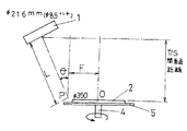
この発明の実施例を図1、2、3、4について説明する。回転軸4の円板5上へ基板2をセットすると共に、基板2の斜め上方へ、スパッタリングカソード1を、その中心軸線Aが、前記基板2の法線Hに対し、θ=30°をなすように架設する。
【0014】
この場合に、基板2の直径は4インチ、ターゲット3の直径は2インチ、基板2の回転軸線Bと、法線Hとの距離Fは60mm、ターゲット3と、基板2の距離Lは300mmであった。
【0015】
前記条件でスパッタリングを行ったところ、基板2の中心からの距離−40〜40mmに対する膜厚分布は±2.0%以下であった(図5)。
【0016】
次に、ターゲット3の配置の異なる他の実施例を説明する。基板2に対し、2個のカソード1a、1bを回転軸Bに対称に配置した実施例である(図2)。また基板2に対し、2個のカソード1a、1bを垂直な平面に対し、面対称に配置した実施例である(図3)。更に基板2に対し、6個のカソード1a、1b、1c、1d、1e、1fを回転軸と垂直面の夫々に対称に配置した実施例である(図4)。
【0017】
図7は、直径9.3インチRMC上に、直径8.5インチのターゲット3を載置したものを用いて、直径350mmの基板にスパッタリングによって薄膜を作製した場合(図6)の膜厚均一性シミュレーション結果である。ここで、図6に示すようにターゲット3の中心と基板2との垂直距離を新たに定義している(T/S間垂直距離と呼ぶ)。T/S間垂直距離はLとθによって決定される(Lcosθ)。これにより、±1.0%以内を確保できるT/S間垂直距離、距離Fを求めることができる。T/S間垂直距離は、装置パラメータとして実際に使用するので、実施例では新たに定義した。
【0018】
また、図7で求めたT/S間垂直距離、距離Fでの膜厚形状シミュレーション結果を示す。このシミュレーションでは直径9.3インチRMCを用いて、直径350mm面内に±0.58%の膜厚分布を得た(図8)。この場合に、実測値をプロットしたところ、前記シミュレーションとほぼ一致し、±0.60%の膜厚分布を得た。
【0019】
次に図9は、T/S間垂直距離380mmでの成膜圧力による膜厚分布依存性を実験したところ、成膜圧力が高くなると膜厚分布が悪くなることが判った。これはスパッタ粒子がスパッタガスの散乱の影響を受けているためと考えられる。
【0020】
そこで、成膜圧力の高い領域で散乱の影響を抑えるためにT/S間垂直距離を近づけて実験を行った。図10は直径350mm面内での膜厚分布のT/S間垂直距離依存性を示すものである。シミュレーションから算出したT/S間垂直距離よりも60mm近づけた結果、膜厚分布で直径350mm面内に±1.0%以下を満たすことができた。
【0021】
従って、膜厚分布はT/S間垂直距離の調整を行うことで膜厚分布を確保することができることが判った。
【0022】
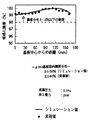
この発明と、従来技術とを比較した。即ち静止対向成膜方式を用いた場合の直径350mm面内においては±1.0%以下の膜厚均一性を得るためのシミュレーションを行った所、図11の結果を得た。図11によれば、静止対向成膜方式で膜厚分布を±1.0%以下にするためには、ターゲットサイズを直径40インチ以上にするか、ターゲット3と基板2との垂直距離を1800mm以上にする必要がある。一方斜入射回転方法を採用すれば、ターゲット3は直径8.5インチであっても、ターゲット3と基板2の垂直距離380mmで膜厚分布±1.0%以下のスパッタリングができる。
【0023】
【発明の効果】
この発明のスパッタリング方法及び装置によれば、基板径よりも小さいターゲット径を用いて基板に生成する膜厚分布、組成比分布、不純物分布を広範囲に均一化できる効果がある。
【0024】
前記により、基板が大径化しても、ターゲットは比較的小径で十分高精度に成膜できると共に、T/S間垂直距離を短縮できるので、装置を小型化することができるなどの諸効果がある。
【図面の簡単な説明】
【図1】この発明の装置の実施例の概念図。
【図2】同じく他の実施例の概念図。
【図3】同じく2個のカソードを垂直面に対称に配置した実施例の概念図。
【図4】同じく数個のカソードを配置した実施例の概念図。
【図5】同じく膜厚−基板中心からの距離グラフ。
【図6】同じく基板とターゲットとの相互関係を示す概念図。
【図7】同じくオフセット距離−T/S間垂直距離のグラフ。
【図8】同じく規格化膜厚−基板中心からの距離グラフ。
【図9】同じく膜厚分布−成膜圧力依存性グラフ。
【図10】同じく膜厚分布−T/S間垂直距離グラフ。
【図11】同じく膜厚分布−T/S間垂直距離グラフ。
【符号の説明】
1 カソード
2 基板
3 ターゲット
A 中心軸線
B 回転軸線
H 法線
D ターゲットの直径
d 基板の直径
F B−H距離
P A−Hの交点
0 基板の中心
V 回転速度[0001]
BACKGROUND OF THE INVENTION
The present invention provides a film thickness distribution, a composition ratio distribution, an impurity attached to a substrate by a target having a diameter equal to or less than the diameter of the substrate in sputtering for semiconductors and various electronic components that require a thin film formation process in vacuum. The present invention relates to a sputtering method and apparatus for the purpose of uniforming the distribution over a wide range and an electronic component manufacturing method .
[0002]
[Prior art]
In the conventional sputtering apparatus, the substrate surface and the target surface are arranged in parallel. In such a conventional sputtering apparatus, a target having a diameter larger than that of the substrate is used in order to make the film thickness distribution, composition ratio distribution, impurity distribution, etc. of the film attached to the substrate uniform over a wide range.
[0003]
In addition, in the multi-source sputtering apparatus in which a plurality of cathodes are inclined with the central axis directed toward the center of the substrate for the purpose of forming an alloy film or a multilayer film, the film thickness distribution, composition ratio distribution, and impurity distribution are poor. It could only be used with a substrate diameter smaller than the target diameter and was used exclusively for research purposes and was not industrial.
[0004]
[Problems to be solved by the invention]
However, since the above-mentioned conventional apparatus had to increase the diameter of the target further as the substrate diameter increased, it is possible to produce the target with the material when the target diameter increases. Some were difficult. For example, Mn and Mn-rich alloys are brittle and easily broken, making it difficult to produce a large target.
[0005]
In addition, if the substrate diameter becomes too large, the influence of the non-erosion region of the target on the film thickness distribution becomes large, etc., so that the film thickness distribution, composition ratio distribution, There is also a problem that the impurity distribution cannot be made uniform.
[0006]
[Means for Solving the Problems]
The present invention comprises a substrate set rotatably and a target,
The diameter of the substrate is d, the diameter of the target is D, the angle formed by the central axis of the target with respect to the normal of the substrate is θ, and the intersection of the central axis of the target and a plane including the surface of the substrate is P, When the distance between the intersection P and the rotation axis of the substrate is F, and the distance between the intersection P and the center of the target is L, the target satisfies the following condition, and the intersection P is outside the substrate. A sputtering apparatus characterized in that one or a plurality are provided at a position to solve the above-mentioned conventional problems, and a uniform film thickness and film quality can be generated even if the target diameter is equal to or less than that of the substrate. It is a thing.
d ≧ D
15 ° ≦ θ ≦ 45 °
50mm ≦ F ≦ 400mm
50mm ≦ L ≦ 800mm
The sputtering apparatus of the present invention includes a plurality of the targets, and the plurality of targets are provided in a rotationally symmetrical manner with respect to the rotation axis of the substrate.
Moreover, this invention provides the sputtering method characterized by performing the film-forming by sputtering on the said board | substrate, rotating the said board | substrate using the sputtering apparatus of the said invention.
Furthermore, the present invention provides a method for manufacturing an electronic component, comprising the step of forming a film by sputtering on the substrate while rotating the substrate using the sputtering apparatus of the present invention.
[0009]
In the present invention, and the normal to the substrate, also the angle θ between the center axis of the target be less than 15 degrees, even if it exceeds 45 degrees, none of the set composition ratio distribution and impurity distribution unevenly It has been found that the film quality is deteriorated.
[0010]
In addition, a decrease in the thin film distribution was observed regardless of whether the distance between the substrate and the target was less than 50 mm or more than 800 mm. Furthermore, the uniformity of the film thickness distribution is poor both when the distance between the intersection axis P of the center axis of the sputtering cathode, the plane including the substrate, and the rotation axis of the substrate is less than 50 mm or more than 400 mm, and the film quality is deteriorated. Admitted. Further, the rotation speed of the substrate varies depending on the sputtering position (distance from the center), but usually exceeds 4 rpm and is preferably less than 60 rpm.
[0011]
DETAILED DESCRIPTION OF THE INVENTION
The present invention includes a target having a diameter D and a center axis A of an angle θ with respect to a normal H of a substrate having a diameter d rotating at an appropriate speed V, and includes the normal H, the center axis A, and the substrate. A method and apparatus for sputtering by appropriately determining an offset distance F of an intersection P with a surface and appropriately setting a distance L between a target and a substrate, the ratio of the substrate diameter d to the target diameter D The numerical values of the angle θ, the distances F, and L are as follows.
[0012]
Rotation speed 4rpm ≦ V ≦ 60rpm
Angle θ 15 ° ≦ θ ≦ 45 °
Diameter d and D d ≧ D
Distance F 50mm ≦ F ≦ 400mm
Distance L 50mm ≦ L ≦ 800mm
[0013]
【Example】
An embodiment of the present invention will be described with reference to FIGS. The
[0014]
In this case, the diameter of the
[0015]
When sputtering was performed under the above conditions, the film thickness distribution with respect to a distance of -40 to 40 mm from the center of the
[0016]
Next, another embodiment in which the arrangement of the
[0017]
FIG. 7 shows a case where a thin film is formed by sputtering on a substrate having a diameter of 350 mm using a
[0018]
Moreover, the film thickness shape simulation result in the T / S vertical distance and distance F calculated | required in FIG. 7 is shown. In this simulation, a film thickness distribution of ± 0.58% was obtained in a 350 mm diameter plane using a 9.3 inch diameter RMC (FIG. 8). In this case, when the actually measured values were plotted, the film thickness distribution of ± 0.60% was obtained almost in agreement with the simulation.
[0019]
Next, in FIG. 9, when the film thickness distribution dependency by the film forming pressure at the T / S vertical distance of 380 mm was tested, it was found that the film thickness distribution deteriorated as the film forming pressure increased. This is presumably because the sputtered particles are affected by the scattering of the sputtering gas.
[0020]
Therefore, in order to suppress the influence of scattering in a region where the film forming pressure is high, an experiment was conducted with the T / S vertical distance being close. FIG. 10 shows the T / S vertical distance dependence of the film thickness distribution within a 350 mm diameter plane. As a result of being closer to 60 mm than the T / S vertical distance calculated from the simulation, it was possible to satisfy ± 1.0% or less in a plane with a diameter of 350 mm in the film thickness distribution.
[0021]
Therefore, it was found that the film thickness distribution can be secured by adjusting the T / S vertical distance.
[0022]
This invention was compared with the prior art. That is, a simulation for obtaining a film thickness uniformity of ± 1.0% or less within a plane of 350 mm in diameter when using the stationary facing film formation method was performed, and the result of FIG. 11 was obtained. According to FIG. 11, in order to reduce the film thickness distribution to ± 1.0% or less in the stationary facing film formation method, the target size is set to 40 inches or more in diameter, or the vertical distance between the
[0023]
【The invention's effect】
According to the sputtering method and apparatus of the present invention, the film thickness distribution to produce a substrate using a smaller target diameter than the substrate diameter, composition ratio distribution is effective that can be extensively homogenize the impurity distribution.
[0024]
As described above, even if the substrate has a large diameter, the target can be formed with a relatively small diameter with sufficiently high accuracy, and the vertical distance between T / S can be shortened, so that the apparatus can be downsized. is there.
[Brief description of the drawings]
FIG. 1 is a conceptual diagram of an embodiment of an apparatus of the present invention.
FIG. 2 is a conceptual diagram of another embodiment.
FIG. 3 is a conceptual diagram of an embodiment in which two cathodes are similarly arranged symmetrically on a vertical plane.
FIG. 4 is a conceptual diagram of an embodiment in which several cathodes are similarly arranged.
FIG. 5 is also a graph of film thickness—distance from the substrate center.
FIG. 6 is a conceptual diagram showing the mutual relationship between the substrate and the target.
FIG. 7 is a graph of the same offset distance-T / S vertical distance.
FIG. 8 is also a normalized film thickness-distance graph from the substrate center.
FIG. 9 is a graph of film thickness distribution-deposition pressure dependency.
FIG. 10 is also a graph of film thickness distribution-T / S vertical distance.
FIG. 11 is also a graph of film thickness distribution-T / S vertical distance.
[Explanation of symbols]
DESCRIPTION OF
Claims (4)
前記基板の直径をd、前記ターゲットの直径をD、前記基板の法線に対する前記ターゲットの中心軸線のなす角度をθ、前記ターゲットの中心軸線と前記基板の表面を含む平面との交点をP、該交点Pと基板の回転軸線との距離をF、前記交点Pと前記ターゲットの中心との距離をLとした時に、前記ターゲットが、以下の条件を満たすと共に、前記交点Pが前記基板の外側となる位置に1又は複数設けられていることを特徴とするスパッタリング装置。The diameter of the substrate is d, the diameter of the target is D, the angle formed by the central axis of the target with respect to the normal of the substrate is θ, and the intersection of the central axis of the target and the plane including the surface of the substrate is P, When the distance between the intersection P and the rotation axis of the substrate is F, and the distance between the intersection P and the center of the target is L, the target satisfies the following condition, and the intersection P is outside the substrate. One or a plurality of sputtering apparatuses are provided at positions where
d≧Dd ≧ D
15°≦θ≦45°15 ° ≦ θ ≦ 45 °
50mm≦F≦400mm50mm ≦ F ≦ 400mm
50mm≦L≦800mm50mm ≦ L ≦ 800mm
Priority Applications (1)
| Application Number | Priority Date | Filing Date | Title |
|---|---|---|---|
| JP00800099A JP4223614B2 (en) | 1999-01-12 | 1999-01-14 | Sputtering method and apparatus, and electronic component manufacturing method |
Applications Claiming Priority (3)
| Application Number | Priority Date | Filing Date | Title |
|---|---|---|---|
| JP11-5084 | 1999-01-12 | ||
| JP508499 | 1999-01-12 | ||
| JP00800099A JP4223614B2 (en) | 1999-01-12 | 1999-01-14 | Sputtering method and apparatus, and electronic component manufacturing method |
Related Child Applications (2)
| Application Number | Title | Priority Date | Filing Date |
|---|---|---|---|
| JP2008229489A Division JP4740299B2 (en) | 1999-01-12 | 2008-09-08 | Sputtering method and apparatus, and electronic component manufacturing method |
| JP2008229523A Division JP4740300B2 (en) | 1999-01-12 | 2008-09-08 | Sputtering method and apparatus, and electronic component manufacturing method |
Publications (3)
| Publication Number | Publication Date |
|---|---|
| JP2000265263A JP2000265263A (en) | 2000-09-26 |
| JP2000265263A5 JP2000265263A5 (en) | 2008-08-21 |
| JP4223614B2 true JP4223614B2 (en) | 2009-02-12 |
Family
ID=26338975
Family Applications (1)
| Application Number | Title | Priority Date | Filing Date |
|---|---|---|---|
| JP00800099A Expired - Lifetime JP4223614B2 (en) | 1999-01-12 | 1999-01-14 | Sputtering method and apparatus, and electronic component manufacturing method |
Country Status (1)
| Country | Link |
|---|---|
| JP (1) | JP4223614B2 (en) |
Families Citing this family (18)
| Publication number | Priority date | Publication date | Assignee | Title |
|---|---|---|---|---|
| JP4502160B2 (en) * | 2000-09-27 | 2010-07-14 | キヤノンアネルバ株式会社 | Magnetic film forming method, magnetic film forming apparatus, and magnetic recording disk manufacturing method |
| KR20040043046A (en) * | 2002-11-15 | 2004-05-22 | 삼성전자주식회사 | Magnetron sputtering apparatus and method thereof |
| JP4673858B2 (en) * | 2005-01-19 | 2011-04-20 | 株式会社アルバック | Sputtering apparatus and film forming method |
| JP2007291506A (en) | 2006-03-31 | 2007-11-08 | Canon Inc | Film deposition method |
| WO2009081953A1 (en) | 2007-12-26 | 2009-07-02 | Canon Anelva Corporation | Sputtering apparatus, sputter film forming method, and analyzer |
| US20110042209A1 (en) * | 2008-06-25 | 2011-02-24 | Canon Anelva Corporation | Sputtering apparatus and recording medium for recording control program thereof |
| WO2010029702A1 (en) * | 2008-09-09 | 2010-03-18 | キヤノンアネルバ株式会社 | Method for manufacturing magnetoresistive element, and storage medium used in the manufacturing method |
| KR101332274B1 (en) | 2008-09-30 | 2013-11-22 | 캐논 아네르바 가부시키가이샤 | Sputtering apparatus and sputtering method |
| WO2010064493A1 (en) | 2008-12-03 | 2010-06-10 | キヤノンアネルバ株式会社 | Plasma processing apparatus, apparatus for manufacturing magnetoresistive element, method for forming magnetic thin film and program for controlling film formation |
| JP5280459B2 (en) * | 2008-12-25 | 2013-09-04 | キヤノンアネルバ株式会社 | Sputtering equipment |
| JP5133232B2 (en) * | 2008-12-26 | 2013-01-30 | 株式会社アルバック | Film forming apparatus and film forming method |
| KR101272009B1 (en) | 2008-12-26 | 2013-06-05 | 캐논 아네르바 가부시키가이샤 | Sputtering equipment, sputtering method and method for manufacturing an electronic device |
| JP5427572B2 (en) * | 2009-12-01 | 2014-02-26 | 昭和電工株式会社 | Magnetron sputtering apparatus, in-line film forming apparatus, and method for manufacturing magnetic recording medium |
| EP2586889A4 (en) | 2010-06-25 | 2016-01-20 | Canon Anelva Corp | Sputtering device, deposition method and control device |
| US20130092528A1 (en) * | 2010-06-30 | 2013-04-18 | Ulvac, Inc. | Film-forming device and film-forming method |
| TW201408803A (en) * | 2012-06-18 | 2014-03-01 | Oc Oerlikon Balzers Ag | PVD apparatus for directional material deposition, methods and workpiece |
| JP2014241417A (en) * | 2014-07-15 | 2014-12-25 | シャープ株式会社 | Aluminum-containing nitride intermediate layer manufacturing method, nitride layer manufacturing method and nitride semiconductor element manufacturing method |
| WO2020137145A1 (en) * | 2018-12-28 | 2020-07-02 | 株式会社アルバック | Film forming device and film forming method |
-
1999
- 1999-01-14 JP JP00800099A patent/JP4223614B2/en not_active Expired - Lifetime
Also Published As
| Publication number | Publication date |
|---|---|
| JP2000265263A (en) | 2000-09-26 |
Similar Documents
| Publication | Publication Date | Title |
|---|---|---|
| JP4223614B2 (en) | Sputtering method and apparatus, and electronic component manufacturing method | |
| JP3408539B2 (en) | Characteristic control of deposited film on semiconductor wafer | |
| JPH036990B2 (en) | ||
| JP2962912B2 (en) | Sputter cathode for coating substrates with cathode sputtering equipment | |
| JP4740300B2 (en) | Sputtering method and apparatus, and electronic component manufacturing method | |
| JPWO2012002473A1 (en) | Film forming apparatus and film forming method | |
| KR20160113185A (en) | Magnetron and magnetron sputtering device | |
| JP6425431B2 (en) | Sputtering method | |
| JPH02251143A (en) | Ion beam type sputtering device | |
| JPS63162862A (en) | Sputtering device | |
| KR20190058269A (en) | Sputtering apparatus | |
| JPS61235560A (en) | Magnetron sputtering device | |
| JP2001323371A (en) | Sputtering system | |
| JP3545050B2 (en) | Sputtering apparatus and sputtering thin film production method | |
| US9449800B2 (en) | Sputtering apparatus and sputtering method | |
| JPH01268867A (en) | Magnetron sputtering device | |
| JP2746292B2 (en) | Sputtering equipment | |
| JP4396885B2 (en) | Magnetron sputtering equipment | |
| JP2000038663A (en) | Magnetron sputtering device | |
| JPS6116346B2 (en) | ||
| JPH02250963A (en) | Sputtering device | |
| JPH01319671A (en) | Multielement sputtering device | |
| JPH0314905B2 (en) | ||
| JPS58100411A (en) | Method of forming ferromagnetic film | |
| JPH0544025A (en) | Circular target for sputtering |
Legal Events
| Date | Code | Title | Description |
|---|---|---|---|
| A621 | Written request for application examination |
Free format text: JAPANESE INTERMEDIATE CODE: A621 Effective date: 20051216 |
|
| A977 | Report on retrieval |
Free format text: JAPANESE INTERMEDIATE CODE: A971007 Effective date: 20080611 |
|
| A521 | Written amendment |
Free format text: JAPANESE INTERMEDIATE CODE: A523 Effective date: 20080704 |
|
| A871 | Explanation of circumstances concerning accelerated examination |
Free format text: JAPANESE INTERMEDIATE CODE: A871 Effective date: 20080704 |
|
| A131 | Notification of reasons for refusal |
Free format text: JAPANESE INTERMEDIATE CODE: A131 Effective date: 20080708 |
|
| RD04 | Notification of resignation of power of attorney |
Free format text: JAPANESE INTERMEDIATE CODE: A7424 Effective date: 20080822 |
|
| A521 | Written amendment |
Free format text: JAPANESE INTERMEDIATE CODE: A523 Effective date: 20080904 Free format text: JAPANESE INTERMEDIATE CODE: A821 Effective date: 20080904 |
|
| RD02 | Notification of acceptance of power of attorney |
Free format text: JAPANESE INTERMEDIATE CODE: A7422 Effective date: 20080904 |
|
| TRDD | Decision of grant or rejection written | ||
| A975 | Report on accelerated examination |
Free format text: JAPANESE INTERMEDIATE CODE: A971005 Effective date: 20081104 |
|
| A01 | Written decision to grant a patent or to grant a registration (utility model) |
Free format text: JAPANESE INTERMEDIATE CODE: A01 Effective date: 20081111 |
|
| A01 | Written decision to grant a patent or to grant a registration (utility model) |
Free format text: JAPANESE INTERMEDIATE CODE: A01 |
|
| A61 | First payment of annual fees (during grant procedure) |
Free format text: JAPANESE INTERMEDIATE CODE: A61 Effective date: 20081120 |
|
| R150 | Certificate of patent or registration of utility model |
Free format text: JAPANESE INTERMEDIATE CODE: R150 |
|
| FPAY | Renewal fee payment (event date is renewal date of database) |
Free format text: PAYMENT UNTIL: 20111128 Year of fee payment: 3 |
|
| FPAY | Renewal fee payment (event date is renewal date of database) |
Free format text: PAYMENT UNTIL: 20111128 Year of fee payment: 3 |
|
| FPAY | Renewal fee payment (event date is renewal date of database) |
Free format text: PAYMENT UNTIL: 20121128 Year of fee payment: 4 |
|
| FPAY | Renewal fee payment (event date is renewal date of database) |
Free format text: PAYMENT UNTIL: 20121128 Year of fee payment: 4 |
|
| FPAY | Renewal fee payment (event date is renewal date of database) |
Free format text: PAYMENT UNTIL: 20131128 Year of fee payment: 5 |
|
| R250 | Receipt of annual fees |
Free format text: JAPANESE INTERMEDIATE CODE: R250 |
|
| R250 | Receipt of annual fees |
Free format text: JAPANESE INTERMEDIATE CODE: R250 |
|
| R250 | Receipt of annual fees |
Free format text: JAPANESE INTERMEDIATE CODE: R250 |
|
| R250 | Receipt of annual fees |
Free format text: JAPANESE INTERMEDIATE CODE: R250 |
|
| R250 | Receipt of annual fees |
Free format text: JAPANESE INTERMEDIATE CODE: R250 |
|
| EXPY | Cancellation because of completion of term |