JP4222260B2 - Lead type electronic component mounting printed circuit board and air conditioner - Google Patents
Lead type electronic component mounting printed circuit board and air conditioner Download PDFInfo
- Publication number
- JP4222260B2 JP4222260B2 JP2004165621A JP2004165621A JP4222260B2 JP 4222260 B2 JP4222260 B2 JP 4222260B2 JP 2004165621 A JP2004165621 A JP 2004165621A JP 2004165621 A JP2004165621 A JP 2004165621A JP 4222260 B2 JP4222260 B2 JP 4222260B2
- Authority
- JP
- Japan
- Prior art keywords
- soldering
- lead
- land
- electronic component
- type electronic
- Prior art date
- Legal status (The legal status is an assumption and is not a legal conclusion. Google has not performed a legal analysis and makes no representation as to the accuracy of the status listed.)
- Expired - Fee Related
Links
Images


Classifications
-
- H—ELECTRICITY
- H05—ELECTRIC TECHNIQUES NOT OTHERWISE PROVIDED FOR
- H05K—PRINTED CIRCUITS; CASINGS OR CONSTRUCTIONAL DETAILS OF ELECTRIC APPARATUS; MANUFACTURE OF ASSEMBLAGES OF ELECTRICAL COMPONENTS
- H05K3/00—Apparatus or processes for manufacturing printed circuits
- H05K3/30—Assembling printed circuits with electric components, e.g. with resistor
- H05K3/32—Assembling printed circuits with electric components, e.g. with resistor electrically connecting electric components or wires to printed circuits
- H05K3/34—Assembling printed circuits with electric components, e.g. with resistor electrically connecting electric components or wires to printed circuits by soldering
- H05K3/3457—Solder materials or compositions; Methods of application thereof
- H05K3/3468—Applying molten solder
-
- H—ELECTRICITY
- H05—ELECTRIC TECHNIQUES NOT OTHERWISE PROVIDED FOR
- H05K—PRINTED CIRCUITS; CASINGS OR CONSTRUCTIONAL DETAILS OF ELECTRIC APPARATUS; MANUFACTURE OF ASSEMBLAGES OF ELECTRICAL COMPONENTS
- H05K1/00—Printed circuits
- H05K1/02—Details
- H05K1/11—Printed elements for providing electric connections to or between printed circuits
- H05K1/111—Pads for surface mounting, e.g. lay-out
-
- H—ELECTRICITY
- H05—ELECTRIC TECHNIQUES NOT OTHERWISE PROVIDED FOR
- H05K—PRINTED CIRCUITS; CASINGS OR CONSTRUCTIONAL DETAILS OF ELECTRIC APPARATUS; MANUFACTURE OF ASSEMBLAGES OF ELECTRICAL COMPONENTS
- H05K1/00—Printed circuits
- H05K1/02—Details
- H05K1/11—Printed elements for providing electric connections to or between printed circuits
- H05K1/115—Via connections; Lands around holes or via connections
- H05K1/116—Lands, clearance holes or other lay-out details concerning the surrounding of a via
-
- H—ELECTRICITY
- H05—ELECTRIC TECHNIQUES NOT OTHERWISE PROVIDED FOR
- H05K—PRINTED CIRCUITS; CASINGS OR CONSTRUCTIONAL DETAILS OF ELECTRIC APPARATUS; MANUFACTURE OF ASSEMBLAGES OF ELECTRICAL COMPONENTS
- H05K2201/00—Indexing scheme relating to printed circuits covered by H05K1/00
- H05K2201/09—Shape and layout
- H05K2201/09209—Shape and layout details of conductors
- H05K2201/09654—Shape and layout details of conductors covering at least two types of conductors provided for in H05K2201/09218 - H05K2201/095
- H05K2201/09681—Mesh conductors, e.g. as a ground plane
-
- H—ELECTRICITY
- H05—ELECTRIC TECHNIQUES NOT OTHERWISE PROVIDED FOR
- H05K—PRINTED CIRCUITS; CASINGS OR CONSTRUCTIONAL DETAILS OF ELECTRIC APPARATUS; MANUFACTURE OF ASSEMBLAGES OF ELECTRICAL COMPONENTS
- H05K2201/00—Indexing scheme relating to printed circuits covered by H05K1/00
- H05K2201/09—Shape and layout
- H05K2201/09209—Shape and layout details of conductors
- H05K2201/09654—Shape and layout details of conductors covering at least two types of conductors provided for in H05K2201/09218 - H05K2201/095
- H05K2201/09781—Dummy conductors, i.e. not used for normal transport of current; Dummy electrodes of components
-
- H—ELECTRICITY
- H05—ELECTRIC TECHNIQUES NOT OTHERWISE PROVIDED FOR
- H05K—PRINTED CIRCUITS; CASINGS OR CONSTRUCTIONAL DETAILS OF ELECTRIC APPARATUS; MANUFACTURE OF ASSEMBLAGES OF ELECTRICAL COMPONENTS
- H05K2203/00—Indexing scheme relating to apparatus or processes for manufacturing printed circuits covered by H05K3/00
- H05K2203/04—Soldering or other types of metallurgic bonding
- H05K2203/046—Means for drawing solder, e.g. for removing excess solder from pads
-
- Y—GENERAL TAGGING OF NEW TECHNOLOGICAL DEVELOPMENTS; GENERAL TAGGING OF CROSS-SECTIONAL TECHNOLOGIES SPANNING OVER SEVERAL SECTIONS OF THE IPC; TECHNICAL SUBJECTS COVERED BY FORMER USPC CROSS-REFERENCE ART COLLECTIONS [XRACs] AND DIGESTS
- Y02—TECHNOLOGIES OR APPLICATIONS FOR MITIGATION OR ADAPTATION AGAINST CLIMATE CHANGE
- Y02P—CLIMATE CHANGE MITIGATION TECHNOLOGIES IN THE PRODUCTION OR PROCESSING OF GOODS
- Y02P70/00—Climate change mitigation technologies in the production process for final industrial or consumer products
- Y02P70/50—Manufacturing or production processes characterised by the final manufactured product
Description
この発明は、噴流式半田槽を用いた半田付により、リード形電子部品が実装されるプリント配線基板に関するものである。 The present invention relates to a printed wiring board on which a lead type electronic component is mounted by soldering using a jet type solder tank.
一般にプリント配線基板は、部品実装密度が細密化が益々要求されていることから、狭ピッチのリード形電子部品等の基板実装化が必要となっている。一方では、環境問題を配慮した鉛フリー半田の実用化が急務となっている。しかしながら鉛フリー半田は、従来から使用している鉛入り共晶半田より半田付け性が悪く、そのため、リード形電子部品等のリード端子間での半田による短絡が発生していた。 In general, a printed wiring board is increasingly required to have a finer component mounting density. Therefore, it is necessary to mount a board with a narrow pitch lead type electronic component. On the other hand, there is an urgent need to put lead-free solder into consideration for environmental issues. However, lead-free solder has poorer solderability than conventional lead-containing eutectic solder, and as a result, a short circuit due to solder has occurred between lead terminals of lead-type electronic components and the like.
従来、この種のプリント配線基板では、半田ブリッジの発生を防止するため、隣接するランドの寸法又は形状を異なる大きさにして、半田に働く表面張力のバランスをくずし、どちらかのランドにはんだを吸収させる方法がとられてきた。(例えば:特許文献1参照) Conventionally, in this type of printed wiring board, in order to prevent the occurrence of solder bridges, the size or shape of adjacent lands is made different so that the balance of surface tension acting on the solder is lost, and solder is applied to either land. Absorption methods have been taken. (For example: see Patent Document 1)
また、両外側のランド部の面積を他よりも大きくすることにより、余剰の半田を両外側の大面積ランドに吸収させる方法がとられてきた。(例えば:特許文献2参照)。 In addition, a method has been employed in which excess solder is absorbed by the large outer lands on both outer sides by making the areas of the outer land portions larger than the others. (For example: see Patent Document 2).
また、噴流式半田付け方向に対して垂直に配置したリード形電子部品の後方側に空きランドを隣接させて、余剰半田を空きランドに吸収させる方法がとられてきた。(例えば:特許文献3参照)。 Further, a method has been adopted in which an empty land is adjacent to the rear side of a lead-type electronic component arranged perpendicular to the jet soldering direction so that excess solder is absorbed by the empty land. (For example: see Patent Document 3).
従来の上述したリード形電子部品実装プリント配線基板は、リード形電子部品の安定したリード間の半田ブリッジの発生しない高品質の半田付を維持するには製造工程の緻密な管理が必要となり、それはリードが狭ピッチになるほど、又半田付け性の悪い鉛フリー半田を使用する場合、より半田付け不良が発生し易く、正確な精度を維持することが困難であった。 The above-described conventional lead-type electronic component mounting printed wiring board requires precise management of the manufacturing process in order to maintain high-quality soldering without the occurrence of a stable solder bridge between the leads of the lead-type electronic component. When lead-free solder having a narrower lead pitch or poor solderability is used, soldering defects are more likely to occur, and it is difficult to maintain accurate accuracy.
この発明は、上述した問題点に鑑みてなされたものであって、狭ピッチのリード形電子部品を半田付する場合にも、より容易な管理の下でリード間の半田ブリッジをより確実に防止することと、半田付不具合の発生を防止することが出来るプリント配線基板を提供することを目的としている。 The present invention has been made in view of the above-described problems, and even when soldering a narrow-pitch lead-type electronic component, the solder bridge between the leads is more reliably prevented under easier management. It is an object of the present invention to provide a printed wiring board capable of preventing the occurrence of soldering defects.
この発明に係るリード形電子部品実装プリント配線基板は、リード形電子部品が装着され、前記リード形電子部品の連続した半田付けランド群を有し、前記リード形電子部品を噴流式半田槽を用いた半田付により、実装着されるプリント配線基板において、前記連続した半田付けランド群を前記噴流式半田付け進行方向に対して前記連続した半田付けランド群の長手方向に沿って配置し、前記連続した半田付けランド群の前記噴流式半田付け進行方向最後尾にランドが格子状に形成された半田引き部を有するとともにこの半田引き部の後方にさらに半田ボイド除去用の平滑面ランドを有する後方半田引きランドを設けたものである。 A printed wiring board mounted with a lead-type electronic component according to the present invention has a lead-type electronic component mounted thereon, has a group of solder lands that are continuous with the lead-type electronic component, and uses the jet-type solder bath for the lead-type electronic component. the have been soldered, in the printed wiring board to be real mounted, placing the consecutive soldering land group the continuous along the longitudinal direction of the soldering land groups with respect to the nozzle-type soldering travel direction, said continuous A rear solder having a soldered portion in which lands are formed in a lattice shape at the end of the jet soldering traveling direction of the soldered land group, and further having a smooth surface land for removing solder voids behind the soldered portion it is provided with a pull land.
この発明のリード形電子部品実装プリント配線基板は、リード形電子部品が装着され、前記リード形電子部品の連続した半田付けランド群を有し、前記リード形電子部品を噴流式半田槽を用いた半田付により、実装着されるプリント配線基板において、前記連続した半田付けランド群を前記噴流式半田付け進行方向に対して前記連続した半田付けランド群の長手方向に沿って配置し、前記連続した半田付けランド群の前記噴流式半田付け進行方向最後尾にランドが格子状に形成された半田引き部を有するとともにこの半田引き部の後方にさらに半田ボイド除去用の平滑面ランドを有する後方半田引きランドを設けた構成としたから、リード形電子部品のはんだ付けランドの半田ブリッジを防止することができる。 The lead-type electronic component mounting printed wiring board of the present invention has a lead-type electronic component mounted thereon and has a group of solder lands that are continuous with the lead-type electronic component. The lead-type electronic component uses a jet solder bath. by soldering in printed circuit board to be real mounted, placing the consecutive soldering land group the continuous along the longitudinal direction of the soldering land groups with respect to the nozzle-type soldering travel direction, said continuous Rear soldering having a soldering portion in which lands are formed in a lattice pattern at the end of the jet soldering direction of the soldering land group and further having a smooth surface land for removing solder voids behind the soldering portion. Since the land is provided, the solder bridge of the soldering land of the lead type electronic component can be prevented.
実施の形態1.
以下に、この発明の実施の形態1によるリード形電子部品実装プリント配線基板について、図1乃至図4により説明する。ここで、図1は、この発明の実施の形態1によるリード形電子部品実装プリント配線基板の裏から見た概略配置構成を示す平面図、図2は、この発明の実施の形態1によるリード形電子部品実装プリント配線基板のリード形電子部品水平配置を示す平面図、図3は、この発明の実施の形態1によるリード形電子部品実装プリント配線基板のリード形電子部品垂直配置を示す平面図、図4は、この発明の実施の形態1によるリード形電子部品実装プリント配線基板の半田付けランド群と後方半田引きランドの関係を示す要部拡大平面図である。
Embodiment 1 FIG.
A lead-type electronic component mounting printed wiring board according to Embodiment 1 of the present invention will be described below with reference to FIGS. Here, FIG. 1 is a plan view showing a schematic arrangement viewed from the back side of the printed wiring board with lead-type electronic components according to the first embodiment of the present invention, and FIG. 2 is a lead shape according to the first embodiment of the present invention. FIG. 3 is a plan view showing a horizontal arrangement of lead-type electronic components on an electronic component-mounted printed wiring board, and FIG. 3 is a plan view showing a vertical arrangement of lead-type electronic components on a lead-type electronic component-mounted printed wiring board according to Embodiment 1 of the present invention; FIG. 4 is an essential part enlarged plan view showing a relationship between a soldering land group and a rear soldering land of the lead-type electronic component mounting printed wiring board according to the first embodiment of the present invention.
図において、プリント配線基板1には、表面に自動実装着される部品(例えば、チップ部品抵抗、チップ部品コンデンサ、チップ部品ダイオード、ディスクリート抵抗、ディスクリートコンデンサ、ディスクリートダイオード等)と、手挿入部品(例えば、大容量抵抗、ハイブリッドIC、トランス、コイル、大容量半導体、大型コンデンサ等)(いずれも図示されていない)が配設されている。 In the figure, the printed wiring board 1 has components that are automatically mounted on the surface (for example, chip component resistors, chip component capacitors, chip component diodes, discrete resistors, discrete capacitors, discrete diodes, etc.) and manually inserted components (for example, , Large-capacity resistors, hybrid ICs, transformers, coils, large-capacity semiconductors, large capacitors, etc. (all not shown) are provided.
また、このプリント配線基板1の裏面には、銅箔(図示されていない)を設け、リード形電子部品群2を矢印で示す方向、即ち、噴流式半田付け進行方向に対して水平又は垂直に実装装着配置されている。
Further, a copper foil (not shown) is provided on the back surface of the printed wiring board 1, and the lead-type
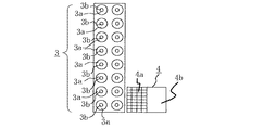
このリード形電子部品群2は、連続した半田付ランド群3を設けると共に、リード形電子部品2を噴流式半田付け進行方向に対して水平に配置した場合、前記連続した半田付ランド群3の後方には前方半分を格子状にし、後方半分を平滑面にした後方半田引きランド4が設けられている。また、リード形電子部品2を噴流式半田付け進行方向に対して垂直に配置した場合、前記連続した半田付ランド群3の個々後方の一部に格子状の半田引きランド4が設けられている。
The lead-type
この発明の実施形態1によるプリント配線基板1の特徴とする点は、従来技術のプリント配線基板における後方半田引込みランド、との形状・配置の相違と、連続した半田付ランド群3のランド形状の相違にある。
The features of the printed wiring board 1 according to the first embodiment of the present invention are the difference in shape and arrangement from the rear solder drawing land in the conventional printed wiring board and the land shape of the continuous
即ち、この発明の実施の形態1によるプリント配線基板1における後方半田引込みランド4は、図4に示すように連続した半田付ランド群3のランド間隔Aと略同じ間隔で配置され、大きさは連続した半田付ランド群3の横2個の長さC×縦2個の長さEの配置面積と略等しい格子状の半田引き部と、そのはんだ引き部と略等しい面積のはんだボイド除去用の平滑面ランドを構成したものである。
That is, the rear solder lead-in
又、後方半田引込みランド4の格子面は、格子パターンの隣同士の間隔Bが0.3mm以内に構成したものが良いとされている。
Further, the lattice surface of the rear
次に、図5はリード形電子部品の噴流式半田付け作業工程を示すフローチャートであり、図5により前述のように構成してからなるプリント配線基板1におけるリード形電子部品2の噴流半田槽を用いた半田付について説明する。先ず、この発明の実施の形態1において、実験・分析によるとプリント配線基板1の表面及び裏面に、ステップS1の自動実実装機部品実装手段において自動実装機により自動実装部品(例えば、チップ部品抵抗、チップ部品コンデンサ、チップ部品ダイオード、ディスクリート抵抗、ディスクリートコンデンサ、ディスクリートダイオード等)(図示されていない)と自動実装対応リード形電子部品2が実装着される。次に、ステップS2の手挿入部品実装手段において、手挿入部品(例えば、大容量抵抗、ハイブリッドIC、トランス、コイル、大容量半導体、大型コンデンサ等)と手実装対応リード形電子部品2が手挿入実装着される。
Next, FIG. 5 is a flow chart showing the lead-type electronic component jet soldering process. FIG. 5 shows a jet solder bath of the lead-type
次に、ステップS3のフラックス塗布手段において、前記リード形電子部品プリント配線基板1の裏面に半田が銅箔になじむようにするフラックス活性剤を塗布する。そしてステップ4のプリヒートにおいて、ステップS3で塗布したフラックスが最良の活性温度となるように加熱するものである。
Next, in the flux applying means in step S3, a flux activator for applying solder to the copper foil is applied to the back surface of the lead-type electronic component printed wiring board 1. Then, in the preheating in
この後、ステップS5の一次半田噴流手段において、リード形電子部品プリント配線基板1の裏面に、多数の穴のあいたノズルから半田を噴水の水のように噴出させる半田噴出手段から、半田を満遍なく部品のリード部分に半田付けする。 Thereafter, in the primary solder jetting means in step S5, the solder is uniformly distributed from the solder jetting means for jetting the solder from the nozzle having many holes on the back surface of the lead-type electronic component printed wiring board 1 like fountain water. Solder to the lead part.
ステップS5の一次半田噴流手段が終わったら、ステップS6の二次半田噴流手段において、一次半田噴流手段で部品のリード間にブリッジした半田を、平らな半田液面を有する半田槽の液面上を図1に示す矢印方向にプリント基板を通過させることによりリード間のブリッジした半田を除去する。最後に、ステップS7の基板冷却において、半田付けされたリード形電子部品プリント配線基板1を冷却すればこの作業は終わりとなる。 After the completion of the primary solder jetting means in step S5, in the secondary solder jetting means in step S6, the solder bridged between the component leads by the primary solder jetting means is moved over the liquid level of the solder bath having a flat solder liquid level. The bridged solder between the leads is removed by passing the printed board in the direction of the arrow shown in FIG. Finally, when the lead-type electronic component printed wiring board 1 that has been soldered is cooled in the board cooling in step S7, this operation is completed.
この実装されたリード形電子部品2は、噴流式半田付け進行方向に対して水平に実装装着配置され、噴流半田槽の半田噴流部へ進入した場合、半田はリード形電子部品2の連続した半田付ランド群3の各半田付ランド3aを伝って後方へ流れる。この時、半田はリード形電子部品2個々のリード端子3bとの表面・界面張力の作用により、次々とブリッジを作りながら後方へ移動する。連続した半田付ランド群3の後方半田は後方半田引きランド4によって引き込まれるが、その際、半田の表面・界面張力の作用により一度引き込んだ連続した半田付ランド群3の後方半田と後方半田引きランド4にそれぞれ戻る力が働く。
The mounted lead-type
ここで、この実施の形態1で提案する後方半田引きランド4を連続した半田付ランド群3のランド間隔Aと略同じ間隔で配置し、大きさは連続した半田付ランド群3の横2個の長さC×縦2個の長さEの配置面積と略等しい後方半田引きランドの格子面4aと、その半田引きランドの格子面4aと略等しい面積の半田ボイド除去用の平滑面4bを構成配置することにより、後方半田引きランド4に半田を引き込みやすくし、更に、一度引き込んだ後方半田引きランド4上の半田の表面・界面張力を分散させて連続した半田付ランド群3に戻る力が少なくなる。その結果、連続した半田付ランド群3の半田ブリッジが大幅に減少する。更に、後方半田引きランド4後方の平滑面により、ボイド状の半田屑の発生をなくすことが、試作評価の結果より効果が確認され、後工程でのボイドを取る手修正作業工程を省くことが可能となり、省工程が実現できる効果がある。
Here, the
後方半田引きランド4を格子形状にせず、従来例通り連続した半田付ランド群3の形状のみを変えたり、連続した半田付ランド群3の両端のランドのみを大きくした場合、この発明の実施の形態よりも連続した半田付ランド群3の半田ショートが非常に多く、特に2列のリード形電子部品ではその現象が顕著であること。また、後方半田引きランド4後方を平滑面にせず、格子形状のみとした場合、ボイド状のはんだ屑の発生が発明者によって確認されている。
When the rear soldering lands 4 are not formed in a lattice shape, only the shape of the continuous
また、噴流式半田付け進行方向に対して垂直に実装装着配置され、噴流半田槽の半田噴流部へ進入した場合、水平配置と同様に半田はリード形電子部品2の半田付ランド群3の各ランドに対して垂直に流れるため各半田付けランド3aの後方への半田の引き込み力が弱く、水平配置に比べてより半田ブリッジが多くなる。
Further, when mounted and arranged perpendicularly to the jet soldering traveling direction and enters the solder jet portion of the jet solder bath, the solder is placed in each of the
ここで、この実施の形態1で提案する後方半田引きランド4を連続した半田付ランド群3の個々後方の一部に、水平配置と同様の形状の後方はんだ引きランド4を配置することにより、半田付ランド群3からのパターン引き出しを阻害することなく、半田付ランド群3個々のランドの半田を、後方半田引きランド4に引き込みやすくし、更に、一度引き込んだ後方半田引きランド4上の半田の表面・界面張力を分散させて連続した半田付ランド群3に戻る力が少なくなる。その結果、連続した半田付ランド群3のパターン引き出しに影響を与えることなく、半田ブリッジが大幅に減少する。後方半田引きランド4を設けず、半田付ランド群3の形状のみを変えたり、半田付ランド群3個々にはんだ引きランドを設けた場合、特に2列のリード形電子部品では、この発明の実施の形態よりも半田付ランド群3の半田ショートが非常に多いことが発明者によって確認されている。
Here, by arranging the rear soldering lands 4 having the same shape as the horizontal arrangement in a part of the individual rear of the soldered
以上のとおり、この発明のリード形電子部品実装プリント配線基板によれば、噴流半田槽を用いて、リード形電子部品の半田付け時に、表面・界面張力によって半田がブリッジを作りながら後方へ移動する際に発生する、半田ショートをより確実になくすことができるとともに、半田ショート発生可能個所の低減ができる効果が得られる。 As described above, according to the lead-type electronic component mounting printed wiring board of the present invention, when the lead-type electronic component is soldered using the jet solder bath, the solder moves backward while forming a bridge by the surface / interface tension. In this case, it is possible to more reliably eliminate solder shorts that occur at the same time, and to reduce the number of places where solder shorts can occur.
図6は、この発明の他の実施の形態によるリード形電子部品実装プリント配線基板を配設した空気調和機の室外機を示す概略正面図である。図において、空気調和機の室外機12は送風機13aを備えた送風機室13と圧縮機14a、扁平形状の電気品室15から成る圧縮機室14とから構成され、前記電気品室15には電気部品15aを装着した表面を下側にし、銅箔を有する平面状態とした裏面を上側にして配置したリード形電子部品実装プリント配線基板1を内蔵している。
FIG. 6 is a schematic front view showing an outdoor unit of an air conditioner provided with a lead type electronic component mounting printed wiring board according to another embodiment of the present invention. In the figure, an
したがって、この発明の他の実施の形態によるリード形電子部品実装プリント配線基板が配置される電気品室を高さ方向を扁平形状にして構成でき、空気調和機の室外機の圧縮機室の電気品箱を扁平にして配置スペースをコンパクトにし、他の部品スペースの組込みに自由度が増し、余裕をもって組み立て作業ができる効果がある。 Therefore, the electrical component room in which the lead-type electronic component mounting printed wiring board according to another embodiment of the present invention is arranged can be configured with a flat shape in the height direction, and the electric of the compressor chamber of the outdoor unit of the air conditioner can be configured. The product box is flattened to make the layout space compact, increasing the degree of freedom for assembling other parts spaces, and enabling assembly work with a margin.
1 プリント配線基板、2 リード形電子部品、3 連続半田付ランド群、3a 半田付ランド、3b リード端子、4 後方半田引きランド、4a 後方半田引付ランドの格子面、4b 後方半田引付ランドの平滑面、12 空気調和機室外機、13 送風機室、14 圧縮機室、15 電気品室。 DESCRIPTION OF SYMBOLS 1 Printed wiring board, 2 lead-type electronic component, 3 continuous soldering land group, 3a soldering land, 3b lead terminal, 4 back soldering land, 4a lattice surface of back soldering land, 4b back soldering land Smooth surface, 12 air conditioner outdoor unit, 13 blower room, 14 compressor room, 15 electrical component room.
Claims (3)
Priority Applications (4)
| Application Number | Priority Date | Filing Date | Title |
|---|---|---|---|
| JP2004165621A JP4222260B2 (en) | 2004-06-03 | 2004-06-03 | Lead type electronic component mounting printed circuit board and air conditioner |
| ES05252366T ES2401585T3 (en) | 2004-06-03 | 2005-04-15 | Printed circuit board, electronic component welding method and air conditioner with printed circuit board |
| EP05252366A EP1603375B1 (en) | 2004-06-03 | 2005-04-15 | Printed circuit board, method of soldering electronic components, and air conditioning apparatus with printed circuit board |
| CNB2005100728005A CN100475002C (en) | 2004-06-03 | 2005-05-20 | Printed circuit board, method of soldering electronic components, and air conditioning apparatus with printed circuit board |
Applications Claiming Priority (1)
| Application Number | Priority Date | Filing Date | Title |
|---|---|---|---|
| JP2004165621A JP4222260B2 (en) | 2004-06-03 | 2004-06-03 | Lead type electronic component mounting printed circuit board and air conditioner |
Publications (3)
| Publication Number | Publication Date |
|---|---|
| JP2005347529A JP2005347529A (en) | 2005-12-15 |
| JP2005347529A5 JP2005347529A5 (en) | 2006-10-12 |
| JP4222260B2 true JP4222260B2 (en) | 2009-02-12 |
Family
ID=34940856
Family Applications (1)
| Application Number | Title | Priority Date | Filing Date |
|---|---|---|---|
| JP2004165621A Expired - Fee Related JP4222260B2 (en) | 2004-06-03 | 2004-06-03 | Lead type electronic component mounting printed circuit board and air conditioner |
Country Status (4)
| Country | Link |
|---|---|
| EP (1) | EP1603375B1 (en) |
| JP (1) | JP4222260B2 (en) |
| CN (1) | CN100475002C (en) |
| ES (1) | ES2401585T3 (en) |
Families Citing this family (2)
| Publication number | Priority date | Publication date | Assignee | Title |
|---|---|---|---|---|
| JP4196979B2 (en) * | 2005-09-07 | 2008-12-17 | 三菱電機株式会社 | Lead-type electronic component mounting printed wiring board, lead-type electronic component soldering method, air conditioner. |
| JP5599151B2 (en) | 2009-01-30 | 2014-10-01 | 三菱電機株式会社 | Double-row lead-type electronic component mounting printed circuit board, double-row lead-type electronic component soldering method, air conditioner |
Family Cites Families (14)
| Publication number | Priority date | Publication date | Assignee | Title |
|---|---|---|---|---|
| DE3211408A1 (en) * | 1982-03-27 | 1983-09-29 | Vdo Adolf Schindling Ag, 6000 Frankfurt | SUBSTRATE |
| JPS62243393A (en) | 1986-04-15 | 1987-10-23 | キヤノン株式会社 | Printed board |
| JPS63157492A (en) | 1986-12-22 | 1988-06-30 | 株式会社東芝 | Printed wiring board |
| US4835345A (en) * | 1987-09-18 | 1989-05-30 | Compaq Computer Corporation | Printed wiring board having robber pads for excess solder |
| JPH01300588A (en) | 1988-05-28 | 1989-12-05 | Nec Home Electron Ltd | Printed wiring board and method of soldering the same |
| US5243143A (en) * | 1990-11-13 | 1993-09-07 | Compaq Computer Corporation | Solder snap bar |
| JP2675473B2 (en) * | 1992-01-13 | 1997-11-12 | 三洋電機株式会社 | Flat package IC Solder dip type printed wiring board |
| FR2714566B1 (en) * | 1993-12-24 | 1996-03-15 | Marelli Autronica | Printed circuit board with improved solder drainage areas. |
| US5604333A (en) * | 1994-11-30 | 1997-02-18 | Intel Corporation | Process and structure for a solder thief on circuit boards |
| JPH08307022A (en) * | 1995-05-10 | 1996-11-22 | Fuji Electric Co Ltd | Printed board |
| KR100319291B1 (en) * | 1999-03-13 | 2002-01-09 | 윤종용 | Printed circuit board and soldering method of printed circuit board |
| JP2002280717A (en) * | 2001-03-19 | 2002-09-27 | Matsushita Graphic Communication Systems Inc | Printed board |
| JP3633505B2 (en) * | 2001-04-27 | 2005-03-30 | 松下電器産業株式会社 | Printed circuit board and printed circuit board soldering method |
| JP3988720B2 (en) * | 2003-12-11 | 2007-10-10 | 三菱電機株式会社 | 4 direction lead flat package IC mounting printed wiring board and soldering method of 4 direction lead flat package IC mounting, air conditioner provided with 4 direction lead flat package IC mounting printed wiring board. |
-
2004
- 2004-06-03 JP JP2004165621A patent/JP4222260B2/en not_active Expired - Fee Related
-
2005
- 2005-04-15 EP EP05252366A patent/EP1603375B1/en not_active Expired - Fee Related
- 2005-04-15 ES ES05252366T patent/ES2401585T3/en active Active
- 2005-05-20 CN CNB2005100728005A patent/CN100475002C/en active Active
Also Published As
| Publication number | Publication date |
|---|---|
| CN100475002C (en) | 2009-04-01 |
| JP2005347529A (en) | 2005-12-15 |
| EP1603375B1 (en) | 2013-03-06 |
| EP1603375A1 (en) | 2005-12-07 |
| ES2401585T3 (en) | 2013-04-22 |
| CN1705428A (en) | 2005-12-07 |
Similar Documents
| Publication | Publication Date | Title |
|---|---|---|
| JP2007048874A (en) | Four-directional lead-flat package ic mounting printed-wiring board, method for soldering same, and air conditioner | |
| US6998861B2 (en) | Wiring board and soldering method therefor | |
| JP4650948B2 (en) | Through-hole soldering structure | |
| JP3988720B2 (en) | 4 direction lead flat package IC mounting printed wiring board and soldering method of 4 direction lead flat package IC mounting, air conditioner provided with 4 direction lead flat package IC mounting printed wiring board. | |
| JP5496118B2 (en) | Soldering method and air conditioner for printed wiring board, 4-way lead flat package IC | |
| JP5807145B2 (en) | Mounting structure | |
| JP4222260B2 (en) | Lead type electronic component mounting printed circuit board and air conditioner | |
| JP5599151B2 (en) | Double-row lead-type electronic component mounting printed circuit board, double-row lead-type electronic component soldering method, air conditioner | |
| JP4196979B2 (en) | Lead-type electronic component mounting printed wiring board, lead-type electronic component soldering method, air conditioner. | |
| JP2009141106A (en) | Printed circuit board, air conditioner, and soldering method for printed circuit board | |
| CN211267300U (en) | Steel mesh and welded structure | |
| JP4041991B2 (en) | Printed wiring board | |
| JP2009283983A (en) | Printed wiring board, air conditioner, and soldering method for printed wiring board | |
| JP2009060006A (en) | Soldering pallet | |
| JP5885162B2 (en) | Printed wiring board | |
| JPH11177224A (en) | Metallic mask and printed wiring board | |
| JPH09232699A (en) | Jumper circuit on single-sided printed circuit board | |
| JP2004207421A (en) | Soldering method of jumper wire |
Legal Events
| Date | Code | Title | Description |
|---|---|---|---|
| A521 | Request for written amendment filed |
Free format text: JAPANESE INTERMEDIATE CODE: A523 Effective date: 20060830 |
|
| A621 | Written request for application examination |
Free format text: JAPANESE INTERMEDIATE CODE: A621 Effective date: 20060830 |
|
| A977 | Report on retrieval |
Free format text: JAPANESE INTERMEDIATE CODE: A971007 Effective date: 20080620 |
|
| A131 | Notification of reasons for refusal |
Free format text: JAPANESE INTERMEDIATE CODE: A131 Effective date: 20080715 |
|
| A521 | Request for written amendment filed |
Free format text: JAPANESE INTERMEDIATE CODE: A523 Effective date: 20080910 |
|
| TRDD | Decision of grant or rejection written | ||
| A01 | Written decision to grant a patent or to grant a registration (utility model) |
Free format text: JAPANESE INTERMEDIATE CODE: A01 Effective date: 20081028 |
|
| A01 | Written decision to grant a patent or to grant a registration (utility model) |
Free format text: JAPANESE INTERMEDIATE CODE: A01 |
|
| A61 | First payment of annual fees (during grant procedure) |
Free format text: JAPANESE INTERMEDIATE CODE: A61 Effective date: 20081110 |
|
| R151 | Written notification of patent or utility model registration |
Ref document number: 4222260 Country of ref document: JP Free format text: JAPANESE INTERMEDIATE CODE: R151 |
|
| FPAY | Renewal fee payment (event date is renewal date of database) |
Free format text: PAYMENT UNTIL: 20111128 Year of fee payment: 3 |
|
| FPAY | Renewal fee payment (event date is renewal date of database) |
Free format text: PAYMENT UNTIL: 20121128 Year of fee payment: 4 |
|
| FPAY | Renewal fee payment (event date is renewal date of database) |
Free format text: PAYMENT UNTIL: 20121128 Year of fee payment: 4 |
|
| FPAY | Renewal fee payment (event date is renewal date of database) |
Free format text: PAYMENT UNTIL: 20131128 Year of fee payment: 5 |
|
| R250 | Receipt of annual fees |
Free format text: JAPANESE INTERMEDIATE CODE: R250 |
|
| R250 | Receipt of annual fees |
Free format text: JAPANESE INTERMEDIATE CODE: R250 |
|
| R250 | Receipt of annual fees |
Free format text: JAPANESE INTERMEDIATE CODE: R250 |
|
| R250 | Receipt of annual fees |
Free format text: JAPANESE INTERMEDIATE CODE: R250 |
|
| R250 | Receipt of annual fees |
Free format text: JAPANESE INTERMEDIATE CODE: R250 |
|
| R250 | Receipt of annual fees |
Free format text: JAPANESE INTERMEDIATE CODE: R250 |
|
| LAPS | Cancellation because of no payment of annual fees |