JP4214005B2 - Photocurable resin composition and front substrate for plasma display panel - Google Patents
Photocurable resin composition and front substrate for plasma display panel Download PDFInfo
- Publication number
- JP4214005B2 JP4214005B2 JP2003172344A JP2003172344A JP4214005B2 JP 4214005 B2 JP4214005 B2 JP 4214005B2 JP 2003172344 A JP2003172344 A JP 2003172344A JP 2003172344 A JP2003172344 A JP 2003172344A JP 4214005 B2 JP4214005 B2 JP 4214005B2
- Authority
- JP
- Japan
- Prior art keywords
- compound
- resin composition
- photocurable resin
- black
- metal
- Prior art date
- Legal status (The legal status is an assumption and is not a legal conclusion. Google has not performed a legal analysis and makes no representation as to the accuracy of the status listed.)
- Expired - Fee Related
Links
Images


Classifications
-
- G—PHYSICS
- G03—PHOTOGRAPHY; CINEMATOGRAPHY; ANALOGOUS TECHNIQUES USING WAVES OTHER THAN OPTICAL WAVES; ELECTROGRAPHY; HOLOGRAPHY
- G03F—PHOTOMECHANICAL PRODUCTION OF TEXTURED OR PATTERNED SURFACES, e.g. FOR PRINTING, FOR PROCESSING OF SEMICONDUCTOR DEVICES; MATERIALS THEREFOR; ORIGINALS THEREFOR; APPARATUS SPECIALLY ADAPTED THEREFOR
- G03F7/00—Photomechanical, e.g. photolithographic, production of textured or patterned surfaces, e.g. printing surfaces; Materials therefor, e.g. comprising photoresists; Apparatus specially adapted therefor
- G03F7/0005—Production of optical devices or components in so far as characterised by the lithographic processes or materials used therefor
- G03F7/0007—Filters, e.g. additive colour filters; Components for display devices
-
- G—PHYSICS
- G03—PHOTOGRAPHY; CINEMATOGRAPHY; ANALOGOUS TECHNIQUES USING WAVES OTHER THAN OPTICAL WAVES; ELECTROGRAPHY; HOLOGRAPHY
- G03F—PHOTOMECHANICAL PRODUCTION OF TEXTURED OR PATTERNED SURFACES, e.g. FOR PRINTING, FOR PROCESSING OF SEMICONDUCTOR DEVICES; MATERIALS THEREFOR; ORIGINALS THEREFOR; APPARATUS SPECIALLY ADAPTED THEREFOR
- G03F7/00—Photomechanical, e.g. photolithographic, production of textured or patterned surfaces, e.g. printing surfaces; Materials therefor, e.g. comprising photoresists; Apparatus specially adapted therefor
- G03F7/004—Photosensitive materials
- G03F7/0045—Photosensitive materials with organic non-macromolecular light-sensitive compounds not otherwise provided for, e.g. dissolution inhibitors
-
- G—PHYSICS
- G03—PHOTOGRAPHY; CINEMATOGRAPHY; ANALOGOUS TECHNIQUES USING WAVES OTHER THAN OPTICAL WAVES; ELECTROGRAPHY; HOLOGRAPHY
- G03F—PHOTOMECHANICAL PRODUCTION OF TEXTURED OR PATTERNED SURFACES, e.g. FOR PRINTING, FOR PROCESSING OF SEMICONDUCTOR DEVICES; MATERIALS THEREFOR; ORIGINALS THEREFOR; APPARATUS SPECIALLY ADAPTED THEREFOR
- G03F7/00—Photomechanical, e.g. photolithographic, production of textured or patterned surfaces, e.g. printing surfaces; Materials therefor, e.g. comprising photoresists; Apparatus specially adapted therefor
- G03F7/004—Photosensitive materials
- G03F7/027—Non-macromolecular photopolymerisable compounds having carbon-to-carbon double bonds, e.g. ethylenic compounds
- G03F7/032—Non-macromolecular photopolymerisable compounds having carbon-to-carbon double bonds, e.g. ethylenic compounds with binders
-
- H—ELECTRICITY
- H01—ELECTRIC ELEMENTS
- H01J—ELECTRIC DISCHARGE TUBES OR DISCHARGE LAMPS
- H01J11/00—Gas-filled discharge tubes with alternating current induction of the discharge, e.g. alternating current plasma display panels [AC-PDP]; Gas-filled discharge tubes without any main electrode inside the vessel; Gas-filled discharge tubes with at least one main electrode outside the vessel
- H01J11/20—Constructional details
- H01J11/22—Electrodes, e.g. special shape, material or configuration
Description
【0001】
【発明の属する技術分野】
本発明は光硬化性樹脂組成物及びプラズマディスプレイパネル用前面基板に関し、特に、プラズマディスプレイパネル(以下、PDPと略称する)の前面基板において、精細な電極回路やブラックパターンを形成するのに有用なアルカリ現像型でかつ光硬化型の組成物、及びそれを用いて白黒二層構造を有するバス電極の黒層(下層)及びブラックマトリックスを形成したPDP用前面基板についての提案である。
【0002】
【従来の技術】
PDPは、プラズマ放電による発光を利用して映像や情報の表示を行なう平面ディスプレイであり、パネル構造、駆動方法によってDC型とAC型に分類される。このPDPによるカラー表示の原理は、リブ(隔壁)によって離間された前面ガラス基板と背面ガラス基板に形成された対向する両電極間のセル空間(放電空間)内でプラズマ放電を生じさせ、各セル空間内に封入されているHe、Xe等のガスの放電により発生する紫外線で背面ガラス基板内面に形成された蛍光体を励起し、3原色の可視光を発生させるものである。
【0003】
以下、添付図面を参照しながら簡単に説明する。
【0004】
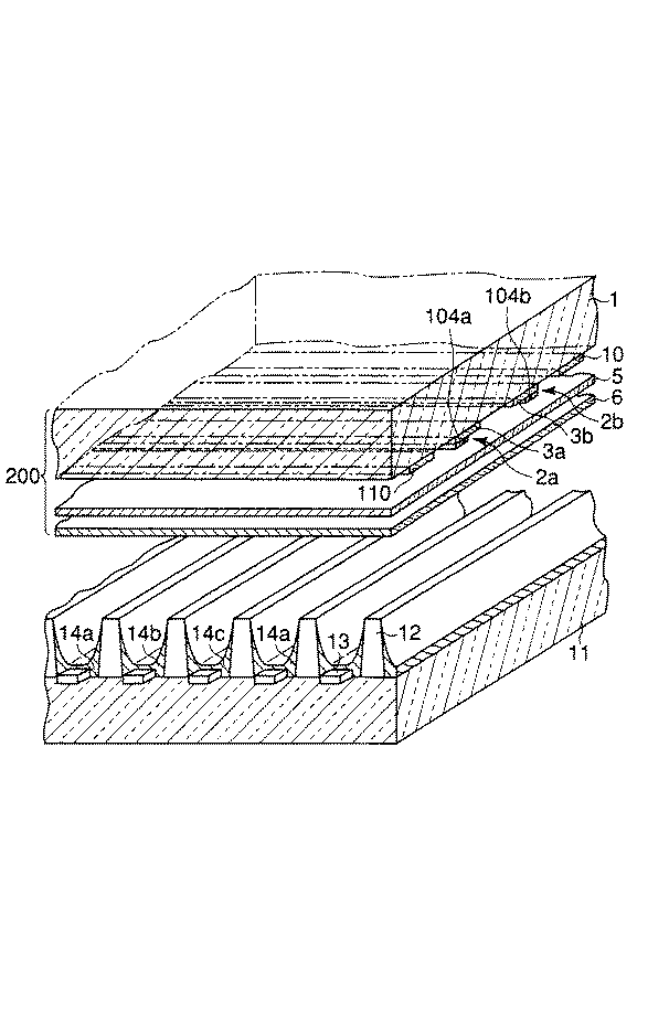
図3は、フルカラー表示の3電極構造の面放電方式PDPの構造例を部分的に示している。前面基板200において、前面ガラス基板1の下面には、放電のための透明電極3a及び3bと該透明電極のライン抵抗を下げるためのバス電極104a及び104bとから成る一対の表示電極2a、2bが所定のピッチで多数列設されている。これらの表示電極2a、2bの下側には、電荷を蓄積するための透明誘電体層(低融点ガラス)5が印刷、焼成によって形成され、その下に保護層(MgO)6が蒸着されている。保護層6は、表示電極の保護、放電状態の維持等の役割を有している。さらに、放電空間を形成する一対の表示電極2a、2bの両側部には、画像のコントラストをさらに高めるために、ストライプ状のブラックマトリックス110が形成されている。
【0005】
一方、背面ガラス基板11の上側には、放電空間を区画するストライプ状のリブ(隔壁)12と各放電空間内に配されたアドレス電極(データ電極)13が所定のピッチで多数列設されている。また、各放電空間の内面には、赤(14a)、青(14b)、緑(14c)の3色の蛍光体膜が規則的に配され、フルカラー表示においては、前記のように赤、青、緑の3原色の蛍光体膜14a、14b、14cで1つの画素が構成される。
【0006】
なお、上記構造のPDPでは、一対の表示電極2aと2bの間に交流のパルス電圧を印加し、同一基板上の電極間で放電させるので、「面放電方式」と呼ばれている。
【0007】
また、上記構造のPDPでは、放電により発生した紫外線が背面基板11の蛍光体膜14a、14b、14cを励起し、発生した可視光を前面基板1の透明電極3a、3bを透して見る構造となっている。
【0008】
このような構造のPDPにおいて、前記バス電極104a、104bの形成は、画面側から見た黒さと導電性を確保するために、従来、銀等を含む高い導電性のペーストからなる白層(上層)(図示せず)と、耐熱性黒顔料と銀等を含む黒色で低い導電性のペーストからなる黒層(下層)(図示せず)をスクリーン印刷した後、パターンマスクを通して露光した後、現像し、次いで焼成する方法が行なわれている。このような方法において黒層用材料に用いられる感光性黒色導電ペーストとしては、耐熱性黒顔料と銀紛を用いて導電性と黒さを両立させた黒色導電ペースト組成物が提案されている(例えば、特許文献1参照)。
【0009】
しかしながら、この黒色導電組成物は、耐熱性黒色顔料に銀が混合されているために充分な黒色が得られないという問題点を有していた。また、該組成物は、銀が混合され導電性を有するがゆえに、ブラックマトリックスの材料として用いると意図しない誤放電が隣接する表示電極間において生じやすく、これを防ぐためにはある程度適切なセル間隔が必要であり、電極回路の高精細化の観点から問題を有していた。
【0010】
ところで、PDPの製造においては、材料利用率の向上並びに製造工程の簡素化による低コスト化を図るべく、バス電極を構成する黒層とブラックマトリックスとを同じ材料を用いて形成する技術が開示されている(例えば、特許文献2参照)。しかしながら、上記黒色導電組成物は導電性を有するため、ブラックマトリックス110を形成する材料として用いることはできず、上記黒色導電性組成物を用いた場合においては該技術の適用による製造工程の簡素化を図ることはできない。
【0011】
【特許文献1】
特開2001−6453号公報
【0012】
【特許文献2】
特開2002−83547号公報
【0013】
【発明が解決しようとする課題】
そこで本発明は、このような従来技術が抱える課題を解決するためになされたものであり、その主たる目的は、光硬化性組成物が白黒2層バス電極の黒層およびブラックマトリックスとして用いることが可能で乾燥、露光、現像、焼成の各工程において基板に対する優れた密着性、解像性、焼成性を損なうことなく、焼成後において充分な黒さを有する焼成皮膜を形成できる光硬化性樹脂組成物を提供することにある。
【0014】
本発明の他の目的は、このような光硬化性樹脂組成物から高精細の電極回路、特に前面基板に形成される白黒2層構造のバス電極において充分な層間導電性(透明電極とバス電極白層との層間導通)と黒さを同時に満足し得る黒層(下層)電極回路、及び充分な黒さを有するブラックマトリックスが形成された高精細なPDP用前面基板を提供することにある。
【0015】
【課題を解決するための手段】
前記目的を達成するために、本発明の光硬化性樹脂組成物の基本的な第一の態様は、(A)耐熱性黒顔料、(B)有機バインダー、(C)光重合性モノマー、(D)光重合開始剤、及び(E)有機金属化合物を含有し、有機金属化合物(E)の配合量が該組成物100質量部当たり金属換算で0.05〜15質量部であり、且つ導電性微粒子を含有しないことを特徴としている。
【0016】
本発明において、前記耐熱性黒顔料(A)は、比表面積が1.0〜20m2/gであり、かつ平均粒子径が5μm以下であることが好ましく、また好適な具体例として四三酸コバルト(Co3O4)が挙げられる。
【0017】
また、本発明において、前記有機金属化合物(E)としては、有機酸金属塩、金属アルコキシド、アルキル金属化合物、アリール金属化合物、グリニアル化合物、金属石鹸、キレート化合物、金属カルボニル化合物、メタロセン化合物、有機金属錯体化合物、メタロセン化合物が挙げられ、錫を含む化合物であることが好ましく、また、その熱分解温度は600℃以下であることが好ましい。
【0018】
このような本発明の光硬化性樹脂組成物は、ペースト状形態であってもよく、また予めフィルム状に製膜したドライフィルムの形態であってもよい。
【0019】
さらに本発明によれば、このような光硬化性樹脂組成物の焼成物から前面基板の黒色電極回路及びブラックマトリックスが形成されてなるPDP用前面基板が提供される。
【0020】
【発明の実施の形態】
本発明者は、前記目的の実現に向け鋭意研究した結果、絶縁性の耐熱性黒顔料を含む光硬化性樹脂組成物に有機金属化合物を添加すると、以下のような効果が生ずることを見出した。すなわち、有機金属化合物を含有する光硬化性樹脂組成物(以下、「本発明の光硬化性樹脂組成物」、又は単に「本発明の組成物」ともいう。)を用いた場合、形成される黒色皮膜に分散した有機金属化合物が、焼成工程において分解して金属を析出させるため、黒色皮膜の抵抗値を下げることができる。このため、白黒2層構造のバス電極の黒層として用いた場合、銀粉等の導電性粒子を配合することなく導電性のバス電極白層と透明電極の層間導通をとることが可能となるとともに、充分な黒さを呈することができる。更に本発明の光硬化性樹脂組成物は導電性微粒子を含有しないためブラックマトリックス用材料として用いた場合に誤放電を防ぐことができる。このように、本発明の光硬化性樹脂組成物は、白黒2層バス電極の黒層およびブラックマトリックスとして用いることが可能で、乾燥、露光、現像、焼成の各工程において基板に対する優れた密着性、解像性、焼成性を損なうことなく、焼成後において充分な黒さを有する焼成皮膜(バス電極の黒層、ブラックマトリックス)を形成し得ることを見出した。
【0021】
このように光硬化性樹脂組成物に、有機金属化合物を添加すると、焼成皮膜が導電性微粒子を含有していなくても、PDP前面基板に形成される白黒2層構造のバス電極において充分な層間導電性(透明電極とバス電極白層との層間導通)を達成できることを見出し、本発明を完成するに至ったものである。
【0022】
従って、本発明の光硬化性樹脂組成物をPDP前面基板に形成される白黒2層構造のバス電極の黒層及びブラックマトリックスの材料として用いれば、バス電極は、黒層がITOやネサなどの透明電極と白層の間に挟持されたサンドイッチ構造を有するため、透明電極と白層との層間導通、並びに画面側から見たときの黒さを共に充分満足させることができるようになる。また、ブラックマトリックスは、画面側から見たときの黒さを充分満足させることができるようになる。更に、バス電極の黒層とブラックマトリックスとが同じ材料を用いて形成されることにより、PDP用前面基板の製造工程の簡素化を図ることが可能となる。
【0023】
図1は、本発明のPDP用前面基板100を含む面放電方式のAC型PDPの構造例を部分的に示したものであり、従来技術の説明において使用した図3と同一機能部分には同一の符号を付した。図1において、上層として導電性の白層(図示せず)22a、22b、下層として黒層(図示せず)21a、21bを有するバス電極4a、4bにおける下層21a、21bと、ブラックマトリックス10とが、本発明の光硬化性樹脂組成物である同一の組成物を用いて形成されている。
【0024】
このような本発明の光硬化性樹脂組成物において、耐熱性黒顔料(A)としては、公知慣用の黒色材料を用いることができ、例えば、Cu、Fe、Mn、Co、Cr等の単独酸化物又は複合酸化物が挙げられ、なかでも四三酸化コバルト(Co3O4)は、焼成時の変色が少なく、焼成後の黒めに優れる点で好ましい。また、これらの耐熱性黒顔料(A)は、2種類以上を併せて用いることができる。
【0025】
耐熱性黒顔料(A)は、電子顕微鏡による任意の10点を測定した平均粒子径が5μm以下、好ましくは0.05μm以上5μm以下の微粒子を用いることが望ましい。この理由は、平均粒子径が5μm以下であると、少量の添加でも、密着性等を損なうことなく緻密な黒色焼成皮膜を形成し得る樹脂組成物を提供することができる。一方、耐熱性黒顔料(A)の平均粒子径が5μmよりも大きくなると、焼成皮膜の緻密性が悪くなり、形成される焼成皮膜の黒色度が低下し易いからである。
【0026】
また、この耐熱性黒顔料(A)は、比表面積が1.0〜25m2/gの範囲にある微粒子を用いることが好ましい。この理由は、その比表面積が1.0m2/g未満では、露光による回路パターン形成の精度が低下し、すなわちラインエッジの直線性が出難くなり、しかも充分な黒さの焼成皮膜が得られ難くなるためである。一方、25m2/gを超える場合、吸油量が大きくなってペーストの流動性が損なわれるため好ましくない。
【0027】
この耐熱性黒顔料(A)の配合量は、有機バインダー(B)100質量部当り0.1〜200質量部、好ましくは20〜100質量部の範囲が適当である。この理由は、黒色微粒子の配合量が0.1質量部よりも少ないと、焼成後に充分な黒さが得られず、一方、200質量部を超える配合量では、光の透過性が劣化する他に、コスト高となり好ましくないからである。
【0028】
前記有機金属化合物(E)としては、有機酸金属塩、金属アルコキシド、アルキル金属化合物、アリール金属化合物、グリニアル化合物、金属石鹸、キレート化合物、金属カルボニル化合物、メタロセン化合物、有機金属錯体化合物、メタロセン化合物などが挙げられ、600℃以下の温度で分解し金属を析出するものが好ましい。熱分解温度が600℃を超える有機金属化合物では、PDPの焼成工程で金属を析出することができず、導電性が得られないので好ましくない。
【0029】
この有機金属化合物(E)の配合量は、組成物100質量部当り金属換算で0.05〜15質量部、好ましくは0.1〜5質量部の範囲が適当である。この理由は、有機金属化合物が0.05質量部未満では十分な導電性が得られず、一方、15質量部を超えると導電性が高くなりすぎ、誤放電を起こすおそれがあるので好ましくない。
【0030】
この有機金属化合物に含まれる金属の種類としては特に限定はされないが、錫が好ましい。これは、焼成過程で錫が析出して酸化すると酸化錫SnO2となり、この酸化錫SnO2は透明であり、黒層の黒色度に影響を与えず、しかも導電性を得ることができるためである。
【0031】
なお、本発明では、耐熱性黒顔料(A)をあらかじめ有機金属化合物(E)で処理し、それを配合することもできる。具体的には、有機金属化合物を溶剤に溶かし耐熱性黒顔料(A)を混合攪拌後、乾燥し耐熱性黒顔料表面に有機金属化合物を付着させたもの、あるいは前記有機金属化合物を付着させた処理物をさらに焼成し耐熱性黒顔料表面に導電性層を形成したもの、などがある。
【0032】
前記有機バインダー(B)としては、カルボキシル基を有する樹脂、具体的にはそれ自体がエチレン性不飽和二重結合を有するカルボキシル基含有感光性樹脂及びエチレン性不飽和二重結合を有さないカルボキシル基含有樹脂のいずれも使用可能である。好適に使用できる樹脂(オリゴマー及びポリマーのいずれでもよい)としては、以下のようなものが挙げられる。
【0033】
(1)(a)不飽和カルボン酸と(b)不飽和二重結合を有する化合物を共重合させることによって得られるカルボキシル基含有樹脂
(2)(a)不飽和カルボン酸と(b)不飽和二重結合を有する化合物の共重合体にエチレン性不飽和基をペンダントとして付加させることによって得られるカルボキシル基含有感光性樹脂
(3)(c)エポキシ基と不飽和二重結合を有する化合物と(b)不飽和二重結合を有する化合物の共重合体に、(a)不飽和カルボン酸を反応させ、生成した2級の水酸基に(d)多塩基酸無水物を反応させて得られるカルボキシル基含有感光性樹脂
(4)(e)不飽和二重結合を有する酸無水物と、それ以外の(b)不飽和二重結合を有する化合物の共重合体に、(f)水酸基と不飽和二重結合を有する化合物を反応させて得られるカルボキシル基含有感光性樹脂
(5)(g)エポキシ化合物と(h)不飽和モノカルボン酸を反応させ、生成した2級の水酸基に(d)多塩基酸無水物を反応させて得られるカルボキシル基含有感光性樹脂
(6)(b)不飽和二重結合を有する化合物とグリシジル(メタ)アクリレートの共重合体のエポキシ基に、(i)1分子中に1つのカルボキシル基を有し、エチレン性不飽和結合を持たない有機酸を反応させ、生成した2級の水酸基に(d)多塩基酸無水物を反応させて得られるカルボキシル基含有樹脂
(7)(j)水酸基含有ポリマーに(d)多塩基酸無水物を反応させて得られるカルボキシル基含有樹脂
(8)(j)水酸基含有ポリマーに(d)多塩基酸無水物を反応させて得られるカルボキシル基含有樹脂に、(c)エポキシ基と不飽和二重結合を有する化合物をさらに反応させて得られるカルボキシル基含有感光性樹脂。
【0034】
また、上記カルボキシル基含有感光性樹脂及びカルボキシル基含有樹脂としては、それぞれ重量平均分子量1,000〜100,000、好ましくは5,000〜70,000、及び酸価50〜250mgKOH/g、かつ、カルボキシル基含有感光性樹脂の場合、その二重結合当量が350〜2,000、好ましくは400〜1,500のものを好適に用いることができる。上記樹脂の分子量が1,000より低い場合、現像時の皮膜の密着性に悪影響を与え、一方、100,000よりも高い場合、現像不良を生じ易いので好ましくない。また、酸価が50mgKOH/gより低い場合、アルカリ水溶液に対する溶解性が不充分で現像不良を生じ易く、一方、250mgKOH/gより高い場合、現像時に皮膜の密着性の劣化や光硬化部(露光部)の溶解が生じるので好ましくない。さらに、カルボキシル基含有感光性樹脂の場合、感光性樹脂の二重結合当量が350よりも小さいと、焼成時に残渣が残り易くなり、一方、2,000よりも大きいと、現像時の作業余裕度が狭く、また光硬化時に高露光量を必要とするので好ましくない。
【0035】
本発明において、光重合性モノマー(C)は組成物の光硬化性の促進及び現像性を向上させるために用いる。このような光重合性モノマー(C)としては、例えば、2−ヒドロキシエチルアクリレート,2−ヒドロキシプロピルアクリレート、ジエチレングリコールジアクリレート、トリエチレングリコールジアクリレート、ポリエチレングリコールジアクリレート、ポリウレタンジアクリレート、トリメチロールプロパントリアクリレート、ペンタエリスリトールトリアクリレート、ペンタエリスリトールテトラアクリレート、トリメチロールプロパンエチレンオキサイド変性トリアクリレート、トリメチロールプロパンプロピレンオキサイド変性トリアクリレート、ジペンタエリスリトールペンタアクリレート、ジペンタエリスリトールヘキサアクリレート及び上記アクリレートに対応する各メタクリレート類;フタル酸、アジピン酸、マレイン酸、イタコン酸、こはく酸、トリメリット酸、テレフタル酸等の多塩基酸とヒドロキシアルキル(メタ)アクリレートとのモノ−、ジ−、トリ−又はそれ以上のポリエステルなどが挙げられるが、特定のものに限定されるものではなく、またこれらを単独で又は2種以上を組み合わせて用いることができる。これらの光重合性モノマーの中でも、1分子中に2個以上のアクリロイル基又はメタクリロイル基を有する多官能モノマーが好ましい。
【0036】
このような光重合性モノマー(C)の配合量は、前記有機バインダー(カルボキシル基含有感光性樹脂及び/又はカルボキシル基含有樹脂)(B)100質量部当り20〜100質量部が適当である。光重合性モノマー(C)の配合量が上記範囲よりも少ない場合、組成物の充分な光硬化性が得られ難くなり、一方、上記範囲を超えて多量になると、皮膜の深部に比べて表面部の光硬化が早くなるため硬化むらを生じ易くなる。
【0037】
前記光重合開始剤(D)としては、例えば、ベンゾイン、ベンゾインメチルエーテル、ベンゾインエチルエーテル、ベンゾインイソプロピルエーテル等のベンゾインとベンゾインアルキルエーテル類;アセトフェノン、2,2−ジメトキシー2−フェニルアセトフェノン、2,2−ジエトキシー2−フェニルアセトフェノン、1,1−ジクロロアセトフェノン等のアセトフェノン類;2−メチル−1−[4−(メチルチオ)フェニル]−2−モルフォリノプロパン−1−オン、2−ベンジル−2−ジメチルアミノ−1−(4−モルフォリノフェニル)−ブタノン−1等のアミノアセトフェノン類;2−メチルアントラキノン、2−エチルアントラキノン、2−t−ブチルアントラキノン、1−クロロアントラキノン等のアントラキノン類;2,4−ジメチルチオキサントン、2,4−ジエチルチオキサントン、2−クロロチオキサントン、2,4−ジイソプロピルチオキサントン等のチオキサントン類;アセトフェノンジメチルケタール、ベンジルジメチルケタール等のケタール類;ベンゾフェノン等のベンゾフェノン類;又はキサントン類;(2,6−ジメトキシベンゾイル)−2,4,4−ペンチルホスフィンオキサイド、ビス(2,4,6−トリメチルベンゾイル)−フェニルフォスフィンオキサイド、2,4,6−トリメチルベンゾイルジフェニルフォスフィンオキサイド、エチル−2,4,6−トリメチルベンゾイルフェニルフォスフィネイト等のフォスフィンオキサイド類;各種パーオキサイド類などが挙げられ、これら公知慣用の光重合開始剤を単独で又は2種以上を組み合わせて用いることができる。これらの光重合開始剤(D)の配合割合は、前記有機バインダー(カルボキシル基含有感光性樹脂及び/又はカルボキシル基含有樹脂)(B)100質量部当り1〜30質量部が適当であり、好ましくは、5〜20質量部である。
【0038】
また、上記のような光重合開始剤(D)は、N,N−ジメチルアミノ安息香酸エチルエステル、N,N−ジメチルアミノ安息香酸イソアミルエステル、ペンチル−4−ジメチルアミノベンゾエート、トリエチルアミン、トリエタノールアミン等の三級アミン類のような光増感剤の1種あるいは2種以上と組み合わせて用いることができる。
【0039】
さらに、より深い光硬化深度を要求される場合、必要に応じて、可視領域でラジカル重合を開始するチバ・スペシャルティ・ケミカルズ社製イルガキュアー784等のチタノセン系光重合開始剤、ロイコ染料等を硬化助剤として組み合わせて用いることができる。
【0040】
さらに、より深い光硬化深度を要求される場合、必要に応じて、熱重合触媒を前記光重合開始剤(D)と併用して用いることができる。この熱重合触媒は、数分から1時間程度にわたって高温におけるエージングにより未硬化の光重合性モノマーを反応させうるものであり、具体的には、過酸化ベンゾイル等の過酸化物、アゾイソブチロニトリル等のアゾ化合物等があり、好ましくは、2,2´−アゾビスイソブチロニトリル、2,2´−アゾビス−2−メチルブチロニトリル、2,2´−アゾビス−2,4−ジバレロニトリル、1´−アゾビス−1−シクロヘキサンカルボニトリル、ジメチル−2,2´−アゾビスイソブチレイト、4,4´−アゾビス−4−シアノバレリックアシッド、2−メチル−2,2´−アゾビスプロパンニトリル、2,4−ジメチル−2,2,2´,2´―アゾビスペンタンニトリル、1,1´−アゾビス(1−アセトキシ−1−フェニルエタン)、2,2,2´,2´−アゾビス(2−メチルブタナミドオキシム)ジヒドロクロライド等が挙げられ、より好ましいものとしては環境にやさしいノンシアン、ノンハロゲンタイプの1,1´−アゾビス(1−アセトキシ−1−フェニルエタン)が挙げられる。
【0041】
本発明の組成物は、必要に応じて軟化点400〜600℃のガラス粉末、シリカ粉末等の無機微粒子を、本発明の光硬化性樹脂組成物の特性を損なわない量的割合で配合することができる。
【0042】
ガラス粉末は、焼成後の導体回路の密着性向上のため、耐熱性黒顔料(A)100質量部当り300質量部以下、好ましくは200質量部以下の割合で添加できる。このガラス粉末としては、ガラス転移点(Tg)300〜500℃、ガラス軟化点(Ts)400〜600℃のものが好ましい。また、解像度の点からは、好ましくは平均粒子径20μm以下、より好ましくは5μm以下のガラス粉末を用いることができる。
【0043】
上記のようなガラス粉末を光硬化性樹脂組成物に添加することにより、露光・現像後の皮膜は600℃以下で容易に焼成可能となる。但し、本発明の組成物では燃焼性の良好な有機バインダーが用いられ、ガラス粉末が溶融する前に脱バインダーが完了するように組成されているものの、ガラス粉末の軟化点が400℃より低いと、これよりも低い温度で溶融が生じて有機バインダーを包み込み易くなり、残存する有機バインダーが分解することによって組成物中にブリスターが生じ易くなるので好ましくない。
【0044】
ガラス粉末としては、酸化鉛、酸化ビスマス、又は酸化亜鉛などを主成分とする非結晶性フリットが好適に使用できる。
【0045】
シリカ粉末としては、特に合成アモルファスシリカ微粉末が望ましく、その具体例としては、日本アエロジル(株)製のAEROSIL(登録商標)50、130、200、200V、200CF、200FAD、300、300CF、380、OX50、TT600、MOX80、MOX170、COK84、日本シリカ工業(株)製のNipsil(登録商標)AQ、AQ−S、VN3、LP、L300、N−300A、ER−R、ER、RS−150、ES、NS、NS−T、NS−P、NS−KR、NS−K、NA、KQ、KM、DS等が挙げられ、これらを単独で又は2種以上を組み合わせて用いることができる。これらの中でも、一次粒子径が5〜50nm、比表面積が50〜500m2/gのものが好ましい。
【0046】
このような合成アモルファスシリカ微粉末は、前記したような光硬化性樹脂組成物に添加すると、焼成工程において骨材して働き焼成時の変形を抑えることができる。
【0047】
本発明の光硬化性樹脂組成物にこのような多量の無機フィラーやガラス粉末を配合した場合、得られる組成物の保存安定性が悪く、ゲル化や流動性の低下により塗布作業性が悪くなる傾向がある。従って、本発明の組成物では、組成物の保存安定性向上のため、無機フィラーやガラス粉末の成分である金属あるいは酸化物粉末との錯体化あるいは塩形成などの効果のある化合物を、安定剤として添加することが好ましい。安定剤としては、硝酸、硫酸、塩酸、ホウ酸等の各種無機酸;ギ酸、酢酸、アセト酢酸、クエン酸、ステアリン酸、マレイン酸、フマル酸、フタル酸、ベンゼンスルホン酸、スルファミン酸等の各種有機酸;リン酸、亜リン酸、次亜リン酸、リン酸メチル、リン酸エチル、リン酸ブチル、リン酸フェニル、亜リン酸エチル、亜リン酸ジフェニル、モノ(2−メタクリロイルオキシエチル)アシッドホスフェート等の各種リン酸化合物(無機リン酸、有機リン酸)などの酸が挙げられ、単独で又は2種以上を組み合わせて用いることができる。このような安定剤は、前記のガラス粉末や無機微粒子(E)100質量部当り0.1〜10質量部の割合で添加することが好ましい。
【0048】
本発明においては、組成物を希釈してペースト化する目的で、適宜の量の有機溶剤を配合することができる。具体的には、メチルエチルケトン、シクロヘキサノンなどのケトン類;トルエン、キシレン、テトラメチルベンゼンなどの芳香族炭化水素類;セロソルブ、メチルセロソルブ、カルビトール、メチルカルビトール、ブチルカルビトール、プロピレングリコールモノメチルエーテル、ジプロピレングリコールモノメチルエーテル、ジプロピレングリコールモノエチルエーテル、トリエチレングリコールモノエチルエーテルなどのグリコールエーテル類;酢酸エチル、酢酸ブチル、セロソルブアセテート、ブチルセロソルブアセテート、カルビトールアセテート、ブチルカルビトールアセテート、プロピレングリコールモノメチルエーテルアセテートなどの酢酸エステル類;エタノール、プロパノール、エチレングリコール、プロピレングリコール、テルピネオールなどのアルコール類;オクタン、デカンなどの脂肪族炭化水素;石油エーテル、石油ナフサ、水添石油ナフサ、ソルベントナフサなどの石油系溶剤が挙げられ、これらを単独で又は2種以上を組み合わせて用いることができる。
【0049】
本発明の光硬化性樹脂組成物は、さらに必要に応じて、シリコーン系、アクリル系等の消泡・レベリング剤、皮膜の密着性向上のためのシランカップリング剤、等の他の添加剤を配合することもできる。さらにまた、必要に応じて、公知慣用の酸化防止剤や、保存時の熱的安定性を向上させるための熱重合禁止剤、焼成時における基板との結合成分としての金属酸化物、ケイ素酸化物、ホウ素酸化物などの微粒子を添加することもできる。
【0050】
このような本発明の光硬化性樹脂組成物は、予めフィルム状に成膜されている場合には基板上にラミネートすればよいが、ペースト状組成物の場合、スクリーン印刷法、バーコーター、ブレードコーターなど適宜の塗布方法で基板、例えばPDPの前面基板となるガラス基板に塗布し、次いで指触乾燥性を得るために熱風循環式乾燥炉、遠赤外線乾燥炉等で例えば約60〜120℃で5〜40分程度乾燥させて有機溶剤を蒸発させ、タックフリーの塗膜を得る。その後、選択的露光、現像、焼成を行なって所定のパターンの黒色電極回路、ブラックマトリックスを形成する。
【0051】
露光工程としては、所定の露光パターンを有するネガマスクを用いた接触露光及び非接触露光が可能である。露光光源としては、ハロゲンランプ、高圧水銀灯、レーザー光、メタルハライドランプ、ブラックランプ、無電極ランプなどが使用される。露光量としては50〜1000mJ/cm2程度が好ましい。
【0052】
現像工程としてはスプレー法、浸漬法等が用いられる。現像液としては、水酸化ナトリウム、水酸化カリウム、炭酸ナトリウム、炭酸カリウム、珪酸ナトリウムなどの金属アルカリ水溶液や、モノエタノールアミン、ジエタノールアミン、トリエタノールアミンなどのアミン水溶液、特に約1.5質量%以下の濃度の希アルカリ水溶液が好適に用いられるが、組成物中のカルボキシル基含有樹脂のカルボキシル基がケン化され、未硬化部(未露光部)が除去されればよく、上記のような現像液に限定されるものではない。また、現像後に不要な現像液の除去のため、水洗や酸中和を行なうことが好ましい。
【0053】
焼成工程においては、現像後の基板を空気中又は窒素雰囲気下で約400〜600℃の加熱処理を行ない、所望のパターンを形成する。なお、この時の昇温速度は、25℃/分以下に設定することが好ましい。
【0054】
バス電極の黒色層(下層)及びブラックマトリックスを本発明の光硬化性樹脂組成物を用い同時形成する工程を含む、本発明のPDP用前面基板の製造方法について説明する。本発明の製造方法は、即ち、本発明の光硬化性樹脂組成物を前面ガラス基板上に塗布、乾燥してバス電極とブラックマトリックスのパターンを露光し、纏めて現像を行い、ブラックマトリックスとバス電極の黒色層(下層)を同時に形成するものである。
【0055】
具体的には、バス電極の形成においては、まず、図2(A)に示すように、予めスパッタリング、イオンプレーティング、化学蒸着、電着等の従来公知の適宜の手段によりITO、SnO2等により透明電極303が形成された前面ガラス基板301に、本発明の光硬化性樹脂組成物を塗布し、乾燥してタックフリーの黒層320を形成する。次に、図2(B)に示すように、形成した黒層320に対し、バス電極とブラックマトリックスのパターンを有するフォトマスク350を重ね合わせ、露光する。次に、図2(C)に示すように、Ag、Au、Al、Pt、Pd等の導電性粉末を含有する導電性の高い組成物を塗布し、乾燥してタックフリーの白層(導電性層)323を形成する。その後、図2(D)に示すように、これにバス電極の露光パターンを有するフォトマスク351を重ね合わせ、露光する。次いで、アルカリ水溶液により現像して非露光部分を除去し、その後、焼成することにより、図2(E)に示すように、透明電極303の上に黒層(下層)電極321と白層(上層)電極322とからなるバス電極304と、ブラックマトリックス310が形成される。
【0056】
なお、図2(B)において、バス電極とブラックマトリックスのパターンを有するフォトマスク350に替えて、ブラックマトリックスのパターンのみを有するフォトマスクを重ね合わせて露光し、図2(D)において、バス電極の露光パターンを有するフォトマスク351に替えて、バス電極とブラックマトリックスのパターンを有するフォトマスクを重ね合わせて白黒2層を同時に露光すること以外は、上記方法と同様にして、バス電極とブラックマトリックスのパターンを形成することもできる。
【0057】
【実施例】
以下、本発明を実施例に基づいて具体的に説明するが、本発明が下記実施例に限定されるものでないことはもとよりである。なお、以下において「部」は、特に断りのない限りすべて質量部であるものとする。
(合成例1)
温度計、攪拌機、滴下ロート、及び還流冷却器を備えたフラスコに、メチルメタクリレートとメタクリル酸を0.87:0.13のモル比で仕込み、溶媒としてトリプロピレングリコールモノメチルエーテルと石油ナフサ(混合比1:1)、触媒としてアゾビスイソブチロニトリルを入れ、窒素雰囲気下、80℃で2〜6時間攪拌し、有機バインダーAを得た。この有機バインダーAは、重量平均分子量が約20,000、酸価が74mgKOH/gであった。
なお、得られた有機バインダーA(共重合樹脂)の重量平均分子量の測定は、島津製作所製ポンプLC−6ADと昭和電工製カラムShodex(登録商標)KF−804、KF−803、KF−802を三本つないだ高速液体クロマトグラフィーにより測定した。
【0058】
このようにして得られた有機バインダーAを用い、以下に示す組成比にて配合し、攪拌機により攪拌後、3本ロールミルにより練肉してペースト化を行なった。
【0059】
なお、低融点ガラス粉末としては、Bi2O3 50%、B2O3 15%、ZnO15%、SiO2 6%、BaO 17%を粉砕し、熱膨張係数α300=85×10-7/℃、ガラス転移点460℃、平均粒子径1.6μmとしたものを使用した。
【0060】
また、本実施例で有機金属化合物として用いたジ-n-ブチルスズジラウリレートは、セイコーインスツルメンツ社製のTG/DTA6200にて、昇温速度10℃/min、空気雰囲気中の条件にて測定した熱分解温度が280℃であった。
【0061】
また、耐熱性黒顔料として四三酸化コバルト(Co3O4)を用い、その比表面積は、マイクロメリテックス製アサップ2010(発売元:島津製作所)にて以下のように測定した。すなわち、0.1g以上2.0g以下の四三酸化コバルト粉末を試料測定管に入れ、試料への窒素ガスの吸着量を測定した。窒素ガスの相対圧力は原則として0.05〜0.2の範囲内の5点以上とした。得られた値に、B.E.T.式を適用し、得られた比表面積の要約データから抽出した。
【0062】
(組成物例2)
ジ-n-ブチルスズジラウリレートを15.0部としたこと以外は、組成物例1と同様の組成にてペースト化を行った。
【0065】
(比較組成物例)
ジ-n-ブチルスズジラウリレートを含めなかったこと以外は、組成物例1と同様の組成にてペースト化を行った。
【0066】
このようにして得られた組成物例1、2及び比較組成物例の各ペーストについて、バス電極評価(抵抗値、層間導通、焼成後色調、L*値)、ブラックマトリックス評価(焼成後色調、L*値)、ペースト安定性の評価を行った。その評価方法は以下のとおりである。
【0067】
抵抗値:
ガラス基板上に、評価用ペーストを200メッシュのポリエステルスクリーンを用いて全面に塗布し、次いで、熱風循環式乾燥炉にて90℃で20分間乾燥して指触乾燥性の良好な塗膜を形成した。次に、この塗膜上に、白層(上層)用導電性ペーストを200メッシュのポリエステルスクリーンを用いて全面に塗布し、次いで、熱風循環式乾燥炉にて90℃で20分間乾燥して指触乾燥性の良好な2層構造の塗膜を形成した。その後、光源をメタルハライドランプとし、パターン寸法100μm×10cmのネガマスクを用いて、組成物上の積算光量が500mJ/cm2となるように露光した後、液温30℃の0.5質量%Na2CO3水溶液を用いて現像を行ない、水洗した。最後に、空気雰囲気下にて5℃/分で昇温し、550℃で30分間焼成し、ガラス基板上に焼成皮膜を形成した。こうして形成した焼成皮膜について抵抗値を測定した。
【0068】
層間導通:
ITO膜付きガラス基板上に、上記と同様の方法により100μm×3cmのパターンの焼成皮膜をスペース100μmで1対形成した。こうして形成した焼成皮膜の白層(上層)にテスターをあて抵抗値の確認を行なった。
【0069】
焼成後色調:
ITO膜付きガラス基板上に、上記と同様の方法(ブラックマトリックス評価については白層(上層)用導電性ペーストを塗布しない)により3cm×10cmのパターンの焼成皮膜を形成した。こうして形成した焼成皮膜をガラス側から目視により観察し、色調の確認を行なった。
【0070】
L*値:
上記焼成後色調を確認した試験片を用いて色彩色差計(ミノルタカメラ(株)製、CR−221)を用いてL*a*b*表色系の値をJIS−Z−8729に従って測定し、明度を表す指数であるL*値を黒色度の指標として評価した。このL*値が小さいほど黒色度に優れる。
【0071】
これらの評価結果を表1に示す。
【0072】
この表1に示す結果から明らかなように、本発明の組成物に係るペーストは、比較組成物のペーストに比べて層間導通に優れ、焼成後においても、充分な黒さを満足し得るバス電極用黒層(下層)、ブラックマトリックスを形成できることがわかった。なお、層間導通は、従来の銀を含む導電性黒ペーストを用いた場合と同レベルであった。
【0073】
【表1】
なお、上記評価用ペーストについて、現像後のライン形状、焼成後のライン形状、密着性を評価したが、いずれも問題はなかった。
【0075】
これらの評価に使用した基板は、ガラス基板上に形成した皮膜を、ライン/スペース=50/100μmとなるガラス乾板を用いてパターン露光し、次いで、液温が30℃の0.5質量%Na2CO3水溶液にて現像を行ない、水洗し、その後、焼成すること以外は、上記抵抗値評価の場合と同様にして焼成皮膜のパターンを形成した基板を作成した。
【0076】
これらの評価方法は、現像後のライン形状については、現像まで終了したパターンを顕微鏡観察し、ラインに不規則なばらつきがなく、よれ等がないかどうかで評価し、焼成後のライン形状については、焼成まで終了したパターンを顕微鏡観察し、ラインに不規則なばらつきがなく、よれ等がないかどうかで評価した。また密着性は、セロハン粘着テープによるピーリングを行ない、パターンの剥離がないかどうかで評価した。
【0077】
【発明の効果】
以上説明したように本発明の光硬化性樹脂組成物によれば、白黒2層バス電極の黒層およびブラックマトリックスとして用いることが可能で乾燥、露光、現像、焼成の各工程において基板に対する優れた密着性、解像性、焼成性を損なうことなく、焼成後において充分な黒さを有する焼成皮膜を形成できる光硬化性樹脂組成物を提供することができる。
【0078】
その結果、本発明によれば、特に前面基板に形成される白黒2層構造のバス電極において充分な層間導電性(透明電極とバス電極白層との層間導通)と黒さを同時に満足し得る黒層(下層)電極回路、及び充分な黒さを有するブラックマトリックスを形成したPDPを提供することができる。
【図面の簡単な説明】
【図1】 本発明の実施の一態様であるPDP用前面基板を含む面放電方式のAC型PDPの部分分解斜視図。
【図2】 本発明の光硬化性樹脂組成物を用いてPDPのバス電極の黒層およびブラックマトリックスを形成する工程例の概略断面図。
【図3】 面放電方式のAC型PDPの部分分解斜視図。
【符号の説明】
1、301・・・前面ガラス基板
2a,2b・・・表示電極、
303,3a,3b・・・透明電極
404,4a,4b・・・バス電極
5・・・透明誘電体層
6・・・保護層
11 背面ガラス基板
12 リブ
13 アドレス電極
14a,14b,14c 蛍光体膜
21、320、321・・・黒層(下層)
22、322、323・・・白層(上層、導電性層)[0001]
BACKGROUND OF THE INVENTION
The present invention relates to a photocurable resin composition and a front substrate for a plasma display panel, and particularly useful for forming fine electrode circuits and black patterns on a front substrate of a plasma display panel (hereinafter referred to as PDP). This is a proposal for a PDP front substrate in which a black layer (lower layer) and a black matrix of a bus electrode having a black and white bilayer structure are formed using an alkali development type and photocurable type composition.
[0002]
[Prior art]
The PDP is a flat display that displays images and information using light emission by plasma discharge, and is classified into a DC type and an AC type according to a panel structure and a driving method. The principle of color display by this PDP is that plasma discharge is generated in a cell space (discharge space) between opposing electrodes formed on the front glass substrate and the back glass substrate separated by ribs (partition walls), and each cell The phosphor formed on the inner surface of the rear glass substrate is excited by ultraviolet rays generated by the discharge of a gas such as He or Xe enclosed in the space to generate visible light of the three primary colors.
[0003]
Hereinafter, it will be briefly described with reference to the accompanying drawings.
[0004]
FIG. 3 partially shows a structural example of a surface discharge type PDP having a three-electrode structure for full color display. In the
[0005]
On the other hand, on the upper side of the
[0006]
In the PDP having the above structure, an alternating pulse voltage is applied between the pair of
[0007]
In the PDP having the above structure, ultraviolet light generated by discharge excites the
[0008]
In the PDP having such a structure, the formation of the
[0009]
However, this black conductive composition has a problem that sufficient black color cannot be obtained because silver is mixed with the heat-resistant black pigment. In addition, since the composition is conductive because silver is mixed, an unintended erroneous discharge is likely to occur between adjacent display electrodes when used as a black matrix material. It is necessary and has a problem from the viewpoint of high definition of the electrode circuit.
[0010]
By the way, in the manufacture of PDP, a technique is disclosed in which the black layer and the black matrix forming the bus electrode are formed using the same material in order to reduce the cost by improving the material utilization rate and simplifying the manufacturing process. (For example, refer to Patent Document 2). However, since the black conductive composition has conductivity, it cannot be used as a material for forming the
[0011]
[Patent Document 1]
JP 2001-6453 A
[0012]
[Patent Document 2]
JP 2002-83547 A
[0013]
[Problems to be solved by the invention]
Therefore, the present invention has been made to solve such problems of the prior art, and its main purpose is that the photocurable composition is used as a black layer and a black matrix of a black and white two-layer bus electrode. A photocurable resin composition capable of forming a fired film having sufficient blackness after firing without impairing excellent adhesion, resolution, and fireability to the substrate in each step of drying, exposure, development, and firing. To provide things.
[0014]
Another object of the present invention is to provide sufficient interlayer conductivity (transparent electrode and bus electrode) in a high-definition electrode circuit, particularly a black and white two-layer bus electrode formed on the front substrate from such a photocurable resin composition. An object of the present invention is to provide a high-definition front substrate for PDP in which a black layer (lower layer) electrode circuit capable of simultaneously satisfying blackness and blackness (interlayer conduction with a white layer) and a black matrix having sufficient blackness are formed.
[0015]
[Means for Solving the Problems]
In order to achieve the above object, a basic first aspect of the photocurable resin composition of the present invention includes (A) a heat-resistant black pigment, (B) an organic binder, (C) a photopolymerizable monomer, ( D) Contains a photopolymerization initiator and (E) an organometallic compoundThe compounding amount of the organometallic compound (E) is 0.05 to 15 parts by mass in terms of metal per 100 parts by mass of the composition, and does not contain conductive fine particles.It is characterized by that.
[0016]
In the present invention, the heat-resistant black pigment (A) has a specific surface area of 1.0 to 20 m.2/ G and an average particle size of 5 μm or less is preferable, and as a specific example, cobalt tetratrioxide (Co3O4).
[0017]
In the present invention, the organometallic compound (E)AsIsOrganic acid metal salt, metal alkoxide, alkyl metal compound, aryl metal compound, grinal compound, metal soap, chelate compound, metal carbonyl compound, metallocene compound, organometallic complex compound, metallocene compound, etc.A compound containing tin is preferable, and the thermal decomposition temperature is preferably 600 ° C. or lower.Yes.
[0018]
Such a photocurable resin composition of the present invention may be in the form of a paste, or may be in the form of a dry film previously formed into a film.
[0019]
Furthermore, according to this invention, the front substrate for PDP in which the black electrode circuit and black matrix of a front substrate are formed from the baked material of such a photocurable resin composition is provided.
[0020]
DETAILED DESCRIPTION OF THE INVENTION
As a result of intensive research aimed at realizing the above object, the present inventors have found that the following effects are produced when an organometallic compound is added to a photocurable resin composition containing an insulating heat-resistant black pigment. . That is, it is formed when a photocurable resin composition containing an organometallic compound (hereinafter also referred to as “the photocurable resin composition of the present invention” or simply “the composition of the present invention”) is used. Since the organometallic compound dispersed in the black film is decomposed and deposits metal in the firing step, the resistance value of the black film can be lowered. For this reason, when it is used as a black layer of a bus electrode having a black and white two-layer structure, it is possible to establish interlayer conduction between the conductive bus electrode white layer and the transparent electrode without blending conductive particles such as silver powder. , Sufficient blackness can be exhibited. Furthermore, since the photocurable resin composition of the present invention does not contain conductive fine particles, it can prevent erroneous discharge when used as a black matrix material. Thus, the photocurable resin composition of the present invention can be used as a black layer and a black matrix of a black and white two-layer bus electrode, and has excellent adhesion to a substrate in each step of drying, exposure, development, and baking. The present inventors have found that a fired film (a black layer of a bus electrode, a black matrix) having sufficient blackness after firing can be formed without impairing resolution and firing properties.
[0021]
Thus, when an organometallic compound is added to the photo-curable resin composition, even if the fired film does not contain conductive fine particles, sufficient interlayers are formed in a black and white two-layer bus electrode formed on the PDP front substrate. It has been found that conductivity (interlayer conduction between a transparent electrode and a bus electrode white layer) can be achieved, and the present invention has been completed.
[0022]
Therefore, if the photo-curable resin composition of the present invention is used as a black layer and black matrix material for a black / white two-layer bus electrode formed on a PDP front substrate, the bus electrode has a black layer made of ITO or NESA. Since the sandwich structure is sandwiched between the transparent electrode and the white layer, both the interlayer conduction between the transparent electrode and the white layer and the blackness when viewed from the screen side can be sufficiently satisfied. Further, the black matrix can sufficiently satisfy the blackness when viewed from the screen side. Furthermore, since the black layer and the black matrix of the bus electrode are formed using the same material, it is possible to simplify the manufacturing process of the front substrate for PDP.
[0023]
FIG. 1 partially shows an example of the structure of a surface discharge AC type PDP including a
[0024]
In the photocurable resin composition of the present invention, a known and commonly used black material can be used as the heat-resistant black pigment (A), for example, single oxidation of Cu, Fe, Mn, Co, Cr, etc. In particular, cobalt tetroxide (Co3O4) Is preferable in that it has little discoloration during firing and is excellent in blackening after firing. These heat-resistant black pigments (A) can be used in combination of two or more.
[0025]
As the heat-resistant black pigment (A), it is desirable to use fine particles having an average particle diameter of 5 μm or less, preferably 0.05 μm or more and 5 μm or less, as measured at any 10 points using an electron microscope. This is because when the average particle size is 5 μm or less, a resin composition capable of forming a dense black fired film without impairing adhesion or the like can be provided even when added in a small amount. On the other hand, when the average particle size of the heat-resistant black pigment (A) is larger than 5 μm, the denseness of the fired film is deteriorated, and the blackness of the formed fired film is likely to be lowered.
[0026]
The heat-resistant black pigment (A) has a specific surface area of 1.0 to 25 m.2It is preferable to use fine particles in the range of / g. This is because the specific surface area is 1.0 m.2If it is less than / g, the accuracy of circuit pattern formation by exposure decreases, that is, the linearity of the line edge is difficult to obtain, and it is difficult to obtain a fired film with sufficient blackness. On the other hand, 25m2When the amount exceeds / g, the oil absorption is increased and the fluidity of the paste is impaired, which is not preferable.
[0027]
The blending amount of the heat-resistant black pigment (A) is 0.1 to 200 parts by weight, preferably 20 to 100 parts by weight per 100 parts by weight of the organic binder (B). The reason for this is that if the amount of black fine particles is less than 0.1 parts by mass, sufficient blackness cannot be obtained after firing. On the other hand, if the amount exceeds 200 parts by mass, the light transmittance deteriorates. In addition, the cost is high, which is not preferable.
[0028]
Examples of the organic metal compound (E) include organic acid metal salts, metal alkoxides, alkyl metal compounds, aryl metal compounds, grinal compounds, metal soaps, chelate compounds, metal carbonyl compounds, metallocene compounds, organometallic complex compounds, metallocene compounds, and the like. Among them, those which decompose at a temperature of 600 ° C. or lower to precipitate a metal are preferable. An organometallic compound having a thermal decomposition temperature exceeding 600 ° C. is not preferable because a metal cannot be deposited in the PDP firing step and conductivity cannot be obtained.
[0029]
The amount of the organometallic compound (E) is 0.05 to 15 parts by mass, preferably 0.1 to 5 parts by mass in terms of metal per 100 parts by mass of the composition. The reason is that if the organometallic compound is less than 0.05 parts by mass, sufficient conductivity cannot be obtained, whereas if it exceeds 15 parts by mass, the conductivity becomes too high and there is a possibility of causing erroneous discharge.
[0030]
The type of metal contained in the organometallic compound is not particularly limited, but tin is preferable. This is because when tin is precipitated and oxidized in the firing process, tin oxide SnO2This tin oxide SnO2This is because it is transparent, does not affect the blackness of the black layer, and can obtain conductivity.
[0031]
In the present invention, the heat-resistant black pigment (A) can be previously treated with the organometallic compound (E) and then blended. Specifically, the organometallic compound is dissolved in a solvent, the heat-resistant black pigment (A) is mixed and stirred, and then dried and the organometallic compound is adhered to the surface of the heat-resistant black pigment, or the organometallic compound is adhered. The processed product is further fired to form a conductive layer on the surface of the heat-resistant black pigment.
[0032]
Examples of the organic binder (B) include a resin having a carboxyl group, specifically, a carboxyl group-containing photosensitive resin having an ethylenically unsaturated double bond and a carboxyl having no ethylenically unsaturated double bond. Any of the group-containing resins can be used. Examples of the resin (which may be either an oligomer or a polymer) that can be suitably used include the following.
[0033]
(1) A carboxyl group-containing resin obtained by copolymerizing (a) an unsaturated carboxylic acid and (b) a compound having an unsaturated double bond
(2) A carboxyl group-containing photosensitive resin obtained by adding an ethylenically unsaturated group as a pendant to a copolymer of (a) an unsaturated carboxylic acid and (b) a compound having an unsaturated double bond
(3) (c) A secondary product produced by reacting a copolymer of an epoxy group and an unsaturated double bond with (b) an unsaturated double bond and (a) an unsaturated carboxylic acid. Carboxyl group-containing photosensitive resin obtained by reacting (d) a polybasic acid anhydride with the hydroxyl group of
(4) A copolymer of (e) an acid anhydride having an unsaturated double bond and the other (b) compound having an unsaturated double bond has (f) a hydroxyl group and an unsaturated double bond. Carboxyl group-containing photosensitive resin obtained by reacting a compound
(5) A carboxyl group-containing photosensitive resin obtained by reacting (g) an epoxy compound with (h) an unsaturated monocarboxylic acid and reacting the resulting secondary hydroxyl group with (d) a polybasic acid anhydride.
(6) (b) An epoxy group of a copolymer of an unsaturated double bond and a glycidyl (meth) acrylate copolymer, (i) having one carboxyl group in one molecule, and having an ethylenically unsaturated bond A carboxyl group-containing resin obtained by reacting an organic acid having no reaction and reacting the resulting secondary hydroxyl group with (d) a polybasic acid anhydride
(7) (j) A carboxyl group-containing resin obtained by reacting a hydroxyl group-containing polymer with (d) a polybasic acid anhydride
(8) (j) Obtained by further reacting a carboxyl group-containing resin obtained by reacting a hydroxyl group-containing polymer with (d) a polybasic acid anhydride, and (c) a compound having an epoxy group and an unsaturated double bond. Carboxyl group-containing photosensitive resin.
[0034]
The carboxyl group-containing photosensitive resin and the carboxyl group-containing resin each have a weight average molecular weight of 1,000 to 100,000, preferably 5,000 to 70,000, and an acid value of 50 to 250 mgKOH / g, and In the case of a carboxyl group-containing photosensitive resin, those having a double bond equivalent of 350 to 2,000, preferably 400 to 1,500 can be suitably used. When the molecular weight of the resin is lower than 1,000, the adhesion of the film during development is adversely affected. On the other hand, when the molecular weight is higher than 100,000, development defects are liable to occur. On the other hand, when the acid value is lower than 50 mgKOH / g, the solubility in an alkaline aqueous solution is insufficient and development failure tends to occur. Part) is not preferable. Further, in the case of a carboxyl group-containing photosensitive resin, if the double bond equivalent of the photosensitive resin is less than 350, a residue is likely to remain at the time of baking, whereas if it is greater than 2,000, a work margin at the time of development. Is narrow, and a high exposure amount is required at the time of photocuring.
[0035]
In the present invention, the photopolymerizable monomer (C) is used for promoting the photocurability of the composition and improving the developability. Examples of such a photopolymerizable monomer (C) include 2-hydroxyethyl acrylate, 2-hydroxypropyl acrylate, diethylene glycol diacrylate, triethylene glycol diacrylate, polyethylene glycol diacrylate, polyurethane diacrylate, trimethylol propane tri Acrylate, pentaerythritol triacrylate, pentaerythritol tetraacrylate, trimethylolpropane ethylene oxide-modified triacrylate, trimethylolpropane propylene oxide-modified triacrylate, dipentaerythritol pentaacrylate, dipentaerythritol hexaacrylate, and the corresponding methacrylates Phthalic acid, adipic acid, malein Mono-, di-, tri- or higher polyesters of polybasic acids such as itaconic acid, succinic acid, trimellitic acid, terephthalic acid and the like and hydroxyalkyl (meth) acrylates. It is not limited and these can be used alone or in combination of two or more. Among these photopolymerizable monomers, polyfunctional monomers having two or more acryloyl groups or methacryloyl groups in one molecule are preferable.
[0036]
The amount of such a photopolymerizable monomer (C) is suitably 20 to 100 parts by mass per 100 parts by mass of the organic binder (carboxyl group-containing photosensitive resin and / or carboxyl group-containing resin) (B). When the blending amount of the photopolymerizable monomer (C) is less than the above range, it is difficult to obtain sufficient photocurability of the composition. On the other hand, when the amount exceeds the above range, the surface is larger than the deep part of the film. Uneven curing is likely to occur because the photocuring of the part is accelerated.
[0037]
Examples of the photopolymerization initiator (D) include benzoin and benzoin alkyl ethers such as benzoin, benzoin methyl ether, benzoin ethyl ether, and benzoin isopropyl ether; acetophenone, 2,2-dimethoxy-2-phenylacetophenone, 2,2 -Acetophenones such as diethoxy-2-phenylacetophenone and 1,1-dichloroacetophenone; 2-methyl-1- [4- (methylthio) phenyl] -2-morpholinopropan-1-one, 2-benzyl-2-dimethyl Aminoacetophenones such as amino-1- (4-morpholinophenyl) -butanone-1; anthraquinones such as 2-methylanthraquinone, 2-ethylanthraquinone, 2-t-butylanthraquinone, 1-chloroanthraquinone; 2 Thioxanthones such as 4-dimethylthioxanthone, 2,4-diethylthioxanthone, 2-chlorothioxanthone, and 2,4-diisopropylthioxanthone; Ketals such as acetophenone dimethyl ketal and benzyldimethyl ketal; Benzophenones such as benzophenone; or xanthones; (2,6-dimethoxybenzoyl) -2,4,4-pentylphosphine oxide, bis (2,4,6-trimethylbenzoyl) -phenylphosphine oxide, 2,4,6-trimethylbenzoyldiphenylphosphine oxide, ethyl Phosphine oxides such as -2,4,6-trimethylbenzoylphenyl phosphinate; various peroxides and the like, and these known and commonly used photopolymerization initiators may be used alone or in combination of two or more. In combination it can be used. The mixing ratio of these photopolymerization initiators (D) is suitably 1 to 30 parts by mass, preferably 100 parts by mass of the organic binder (carboxyl group-containing photosensitive resin and / or carboxyl group-containing resin) (B). Is 5 to 20 parts by mass.
[0038]
The photopolymerization initiator (D) as described above is composed of N, N-dimethylaminobenzoic acid ethyl ester, N, N-dimethylaminobenzoic acid isoamyl ester, pentyl-4-dimethylaminobenzoate, triethylamine, triethanolamine. It can be used in combination with one or more photosensitizers such as tertiary amines.
[0039]
Furthermore, when a deeper photocuring depth is required, a titanocene photopolymerization initiator such as Irgacure 784 manufactured by Ciba Specialty Chemicals, which starts radical polymerization in the visible region, and leuco dyes are cured as necessary. It can be used in combination as an auxiliary agent.
[0040]
Furthermore, when a deeper photocuring depth is required, a thermal polymerization catalyst can be used in combination with the photopolymerization initiator (D) as necessary. This thermal polymerization catalyst is capable of reacting an uncured photopolymerizable monomer by aging at a high temperature for several minutes to about 1 hour. Specifically, a peroxide such as benzoyl peroxide, azoisobutyronitrile, etc. Azo compounds such as 2,2′-azobisisobutyronitrile, 2,2′-azobis-2-methylbutyronitrile, 2,2′-azobis-2,4-gibarero Nitrile, 1'-azobis-1-cyclohexanecarbonitrile, dimethyl-2,2'-azobisisobutyrate, 4,4'-azobis-4-cyanovaleric acid, 2-methyl-2,2'-azo Bispropanenitrile, 2,4-dimethyl-2,2,2 ′, 2′-azobispentanenitrile, 1,1′-azobis (1-acetoxy-1-phenylethane), 2, , 2 ′, 2′-azobis (2-methylbutanamide oxime) dihydrochloride and the like, and more preferable are environmentally friendly non-cyanide and non-halogen type 1,1′-azobis (1-acetoxy-1-phenyl) Ethane).
[0041]
In the composition of the present invention, inorganic fine particles such as glass powder and silica powder having a softening point of 400 to 600 ° C. are blended in a quantitative ratio that does not impair the characteristics of the photocurable resin composition of the present invention as necessary. Can do.
[0042]
The glass powder can be added at a ratio of 300 parts by mass or less, preferably 200 parts by mass or less, per 100 parts by mass of the heat-resistant black pigment (A) in order to improve the adhesion of the conductor circuit after firing. The glass powder preferably has a glass transition point (Tg) of 300 to 500 ° C. and a glass softening point (Ts) of 400 to 600 ° C. From the viewpoint of resolution, glass powder having an average particle diameter of preferably 20 μm or less, more preferably 5 μm or less can be used.
[0043]
By adding the glass powder as described above to the photocurable resin composition, the film after exposure and development can be easily baked at 600 ° C. or less. However, in the composition of the present invention, a combustible organic binder is used, and the composition is such that debinding is completed before the glass powder melts, but the softening point of the glass powder is lower than 400 ° C. It is not preferable because melting occurs at a temperature lower than this and the organic binder is easily wrapped and blisters are easily formed in the composition by the decomposition of the remaining organic binder.
[0044]
As the glass powder, an amorphous frit containing lead oxide, bismuth oxide, zinc oxide or the like as a main component can be preferably used.
[0045]
As the silica powder, synthetic amorphous silica fine powder is particularly desirable, and specific examples thereof include AEROSIL (registered trademark) 50, 130, 200, 200V, 200CF, 200FAD, 300, 300CF, 380, manufactured by Nippon Aerosil Co., Ltd. OX50, TT600, MOX80, MOX170, COK84, Nippon Silk Industries, Ltd. Nipsil (registered trademark) AQ, AQ-S, VN3, LP, L300, N-300A, ER-R, ER, RS-150, ES NS, NS-T, NS-P, NS-KR, NS-K, NA, KQ, KM, DS and the like, and these can be used alone or in combination of two or more. Among these, the primary particle diameter is 5 to 50 nm, and the specific surface area is 50 to 500 m.2/ G is preferred.
[0046]
When such a synthetic amorphous silica fine powder is added to the photocurable resin composition as described above, it can act as an aggregate in the firing step and suppress deformation during firing.
[0047]
When such a large amount of inorganic filler or glass powder is blended with the photocurable resin composition of the present invention, the storage stability of the resulting composition is poor, and the coating workability deteriorates due to gelation and fluidity deterioration. Tend. Therefore, in the composition of the present invention, in order to improve the storage stability of the composition, a compound having an effect of complexing or forming a salt with a metal or oxide powder as a component of an inorganic filler or glass powder is used as a stabilizer. It is preferable to add as. Stabilizers include various inorganic acids such as nitric acid, sulfuric acid, hydrochloric acid and boric acid; various acids such as formic acid, acetic acid, acetoacetic acid, citric acid, stearic acid, maleic acid, fumaric acid, phthalic acid, benzenesulfonic acid, sulfamic acid Organic acids: phosphoric acid, phosphorous acid, hypophosphorous acid, methyl phosphate, ethyl phosphate, butyl phosphate, phenyl phosphate, ethyl phosphite, diphenyl phosphite, mono (2-methacryloyloxyethyl) acid Acids, such as various phosphoric acid compounds (inorganic phosphoric acid, organic phosphoric acid), such as a phosphate, are mentioned, It can use individually or in combination of 2 or more types. Such a stabilizer is preferably added at a ratio of 0.1 to 10 parts by mass per 100 parts by mass of the glass powder or inorganic fine particles (E).
[0048]
In the present invention, an appropriate amount of an organic solvent can be blended for the purpose of diluting the composition into a paste. Specifically, ketones such as methyl ethyl ketone and cyclohexanone; aromatic hydrocarbons such as toluene, xylene and tetramethylbenzene; cellosolve, methyl cellosolve, carbitol, methyl carbitol, butyl carbitol, propylene glycol monomethyl ether, di Glycol ethers such as propylene glycol monomethyl ether, dipropylene glycol monoethyl ether, triethylene glycol monoethyl ether; ethyl acetate, butyl acetate, cellosolve acetate, butyl cellosolve acetate, carbitol acetate, butyl carbitol acetate, propylene glycol monomethyl ether acetate Acetic acid esters such as ethanol, propanol, ethylene glycol, propylene glycol And alcohols such as terpineol; aliphatic hydrocarbons such as octane and decane; petroleum solvents such as petroleum ether, petroleum naphtha, hydrogenated petroleum naphtha, and solvent naphtha. These may be used alone or in combination of two or more. Can be used.
[0049]
The photo-curable resin composition of the present invention may further contain other additives such as a silicone-based, acrylic-based defoaming / leveling agent, and a silane coupling agent for improving film adhesion, if necessary. It can also be blended. Furthermore, if necessary, known and conventional antioxidants, thermal polymerization inhibitors for improving the thermal stability during storage, metal oxides and silicon oxides as a binding component to the substrate during firing Fine particles such as boron oxide can also be added.
[0050]
Such a photocurable resin composition of the present invention may be laminated on a substrate when it is previously formed into a film, but in the case of a paste-like composition, a screen printing method, a bar coater, a blade It is applied to a substrate such as a coater by an appropriate coating method, for example, a glass substrate that is a front substrate of a PDP, and then in a hot air circulating drying furnace, a far infrared drying furnace, etc., for example at about 60 to 120 ° C. The organic solvent is evaporated by drying for about 5 to 40 minutes to obtain a tack-free coating film. Thereafter, selective exposure, development, and baking are performed to form a black electrode circuit and a black matrix having a predetermined pattern.
[0051]
As the exposure step, contact exposure and non-contact exposure using a negative mask having a predetermined exposure pattern are possible. As the exposure light source, a halogen lamp, a high-pressure mercury lamp, a laser beam, a metal halide lamp, a black lamp, an electrodeless lamp, or the like is used. The exposure amount is 50 to 1000 mJ / cm2The degree is preferred.
[0052]
As the development process, a spray method, an immersion method, or the like is used. Developers include aqueous alkali metal solutions such as sodium hydroxide, potassium hydroxide, sodium carbonate, potassium carbonate and sodium silicate, and aqueous amine solutions such as monoethanolamine, diethanolamine and triethanolamine, especially about 1.5% by mass or less. A dilute alkaline aqueous solution having a concentration of 1 is preferably used, as long as the carboxyl group of the carboxyl group-containing resin in the composition is saponified and the uncured part (unexposed part) is removed. It is not limited to. Further, it is preferable to perform washing with water and acid neutralization in order to remove unnecessary developer after development.
[0053]
In the baking step, the substrate after development is subjected to heat treatment at about 400 to 600 ° C. in air or in a nitrogen atmosphere to form a desired pattern. In addition, it is preferable to set the temperature increase rate at this time to 25 degrees C / min or less.
[0054]
The method for producing the front substrate for PDP of the present invention, which includes the step of simultaneously forming the black layer (lower layer) and the black matrix of the bus electrode using the photocurable resin composition of the present invention, will be described. In the production method of the present invention, the photocurable resin composition of the present invention is applied to a front glass substrate and dried to expose a pattern of bus electrodes and a black matrix, and development is performed collectively. The black layer (lower layer) of the electrode is formed simultaneously.
[0055]
Specifically, in forming the bus electrode, first, as shown in FIG. 2 (A), ITO, SnO are previously formed by a conventionally known appropriate means such as sputtering, ion plating, chemical vapor deposition, electrodeposition or the like.2The photocurable resin composition of the present invention is applied to the
[0056]
Note that in FIG. 2B, instead of the
[0057]
【Example】
EXAMPLES Hereinafter, although this invention is demonstrated concretely based on an Example, it cannot be overemphasized that this invention is not limited to the following Example. In the following, “parts” are all parts by mass unless otherwise specified.
(Synthesis Example 1)
In a flask equipped with a thermometer, stirrer, dropping funnel, and reflux condenser, methyl methacrylate and methacrylic acid were charged at a molar ratio of 0.87: 0.13, and tripropylene glycol monomethyl ether and petroleum naphtha (mixing ratio) were used as solvents. 1: 1), azobisisobutyronitrile was added as a catalyst, and the mixture was stirred at 80 ° C. for 2 to 6 hours in a nitrogen atmosphere to obtain an organic binder A. This organic binder A had a weight average molecular weight of about 20,000 and an acid value of 74 mgKOH / g.
In addition, the measurement of the weight average molecular weight of the obtained organic binder A (copolymerization resin) measured Shimadzu Corporation pump LC-6AD and Showa Denko column Shodex (trademark) KF-804, KF-803, KF-802. The measurement was performed by high performance liquid chromatography connected to a triplet.
[0058]
The organic binder A thus obtained was blended at the composition ratio shown below, stirred with a stirrer, and then kneaded with a three-roll mill to form a paste.
[0059]
As the low melting point glass powder, Bi2OThree 50%, B2OThree 15%, ZnO 15%,
[0060]
Further, di-n-butyltin dilaurate used as an organometallic compound in this example was measured with a TG / DTA6200 manufactured by Seiko Instruments Inc. under conditions of a temperature rising rate of 10 ° C./min and in an air atmosphere. The thermal decomposition temperature was 280 ° C.
[0061]
Further, as a heat resistant black pigment, cobalt trioxide (Co3O4), And the specific surface area was measured by Micromerex Asap 2010 (Sold by: Shimadzu Corporation) as follows. That is, 0.1 g or more and 2.0 g or less of cobalt trioxide powder was placed in a sample measuring tube, and the amount of nitrogen gas adsorbed on the sample was measured. As a general rule, the relative pressure of nitrogen gas was 5 points or more within the range of 0.05 to 0.2. The BET formula was applied to the values obtained and extracted from the summary data of the specific surface area obtained.
[0062]
(Composition Example 2)
Pasting was performed with the same composition as in Composition Example 1 except that 15.0 parts of di-n-butyltin dilaurate was used.
[0065]
(Comparative composition example)
Pasting was performed with the same composition as in Composition Example 1 except that di-n-butyltin dilaurate was not included.
[0066]
For each paste of Composition Examples 1 and 2 and Comparative Composition Example thus obtained, bus electrode evaluation (resistance value, interlayer conduction, color tone after firing, L*Value), black matrix evaluation (color tone after firing, L*Value) and paste stability was evaluated. The evaluation method is as follows.
[0067]
Resistance value:
An evaluation paste is applied on the entire surface of a glass substrate using a 200-mesh polyester screen, and then dried at 90 ° C. for 20 minutes in a hot-air circulating drying oven to form a coating film with good touch drying properties. did. Next, a white layer (upper layer) conductive paste is applied to the entire surface of the coating film using a 200-mesh polyester screen, and then dried at 90 ° C. for 20 minutes in a hot air circulating drying oven. A two-layer coating film having good touch drying properties was formed. Then, using a metal halide lamp as the light source and using a negative mask with a pattern size of 100 μm × 10 cm, the integrated light amount on the composition was 500 mJ / cm.2After exposure to 0.5 wt% Na at a liquid temperature of 30 ° C.2CO3Development was performed using an aqueous solution and washed with water. Finally, the temperature was raised at 5 ° C./min in an air atmosphere and baked at 550 ° C. for 30 minutes to form a fired film on the glass substrate. The resistance value of the fired film thus formed was measured.
[0068]
Interlayer conduction:
A pair of fired films having a pattern of 100 μm × 3 cm was formed on a glass substrate with an ITO film in a space of 100 μm by the same method as described above. The resistance value was confirmed by applying a tester to the white layer (upper layer) of the fired film thus formed.
[0069]
Color after firing:
A fired film having a pattern of 3 cm × 10 cm was formed on a glass substrate with an ITO film by a method similar to the above (without applying a white layer (upper layer) conductive paste for black matrix evaluation). The fired film thus formed was visually observed from the glass side to confirm the color tone.
[0070]
L*value:
L using a color difference meter (manufactured by Minolta Camera Co., Ltd., CR-221) using the test piece whose color tone was confirmed after firing.*a*b*The value of the color system is measured according to JIS-Z-8729, and L is an index representing lightness.*The value was evaluated as an index of blackness. This L*The smaller the value, the better the blackness.
[0071]
These evaluation results are shown in Table 1.
[0072]
As is clear from the results shown in Table 1, the paste according to the composition of the present invention is superior in interlayer conduction as compared with the paste of the comparative composition, and can satisfy a sufficient blackness even after firing. It was found that a black layer (lower layer) and a black matrix can be formed. Interlayer conduction was the same level as when a conventional conductive black paste containing silver was used.
[0073]
[Table 1]
In addition, about the said evaluation paste, although the line shape after image development, the line shape after baking, and adhesiveness were evaluated, all did not have a problem.
[0075]
The substrate used for these evaluations was a pattern exposure of the film formed on the glass substrate using a glass dry plate with line / space = 50/100 μm, and then the liquid temperature was 30 ° C. and 0.5 mass% Na.2CO3A substrate having a fired film pattern was prepared in the same manner as in the above resistance value evaluation except that development was performed with an aqueous solution, washing was performed, and then firing was performed.
[0076]
These evaluation methods are as follows: For the line shape after development, the pattern that has been completed up to development is observed with a microscope, and the line is evaluated for irregularity, whether there is any distortion, etc. Then, the pattern after the firing was observed with a microscope, and it was evaluated whether or not there was no irregular variation in the line and there was no twist or the like. The adhesion was evaluated by peeling with a cellophane pressure-sensitive adhesive tape and checking for pattern peeling.
[0077]
【The invention's effect】
As described above, according to the photocurable resin composition of the present invention, it can be used as a black layer and a black matrix of a black and white two-layer bus electrode, and is excellent for a substrate in each step of drying, exposure, development, and baking. A photocurable resin composition capable of forming a fired film having sufficient blackness after firing without impairing adhesion, resolution, and fireability can be provided.
[0078]
As a result, according to the present invention, sufficient interlevel conductivity (interlayer conduction between the transparent electrode and the white layer of the bus electrode) and blackness can be satisfied at the same time, particularly in the black and white bus layer bus electrode formed on the front substrate. A PDP in which a black layer (lower layer) electrode circuit and a black matrix having sufficient blackness are formed can be provided.
[Brief description of the drawings]
FIG. 1 is a partially exploded perspective view of a surface discharge AC type PDP including a PDP front substrate according to an embodiment of the present invention.
FIG. 2 is a schematic cross-sectional view of a process example for forming a black layer and a black matrix of a PDP bus electrode using the photocurable resin composition of the present invention.
FIG. 3 is a partially exploded perspective view of a surface discharge AC type PDP.
[Explanation of symbols]
1, 301 ... front glass substrate
2a, 2b ... display electrodes,
303, 3a, 3b ... Transparent electrodes
404, 4a, 4b ... bus electrodes
5 ... Transparent dielectric layer
6 ... Protective layer
11 Back glass substrate
12 Ribs
13 Address electrode
14a, 14b, 14c phosphor film
21, 320, 321 ... Black layer (lower layer)
22, 322, 323 ... White layer (upper layer, conductive layer)
Claims (7)
Priority Applications (4)
| Application Number | Priority Date | Filing Date | Title |
|---|---|---|---|
| JP2003172344A JP4214005B2 (en) | 2003-06-17 | 2003-06-17 | Photocurable resin composition and front substrate for plasma display panel |
| TW093117379A TW200502990A (en) | 2003-06-17 | 2004-06-16 | Photo-curable resin composition and front substrate for plasma display panel |
| CN2004100552022A CN1574163B (en) | 2003-06-17 | 2004-06-17 | Photocured resin composition and former substrate of plasm display board |
| KR1020040044830A KR101113464B1 (en) | 2003-06-17 | 2004-06-17 | Photo-Curable Resin Composition and Front Substrate for Plasma Display Panel |
Applications Claiming Priority (1)
| Application Number | Priority Date | Filing Date | Title |
|---|---|---|---|
| JP2003172344A JP4214005B2 (en) | 2003-06-17 | 2003-06-17 | Photocurable resin composition and front substrate for plasma display panel |
Publications (2)
| Publication Number | Publication Date |
|---|---|
| JP2005011584A JP2005011584A (en) | 2005-01-13 |
| JP4214005B2 true JP4214005B2 (en) | 2009-01-28 |
Family
ID=34096530
Family Applications (1)
| Application Number | Title | Priority Date | Filing Date |
|---|---|---|---|
| JP2003172344A Expired - Fee Related JP4214005B2 (en) | 2003-06-17 | 2003-06-17 | Photocurable resin composition and front substrate for plasma display panel |
Country Status (4)
| Country | Link |
|---|---|
| JP (1) | JP4214005B2 (en) |
| KR (1) | KR101113464B1 (en) |
| CN (1) | CN1574163B (en) |
| TW (1) | TW200502990A (en) |
Families Citing this family (5)
| Publication number | Priority date | Publication date | Assignee | Title |
|---|---|---|---|---|
| US7615581B2 (en) * | 2005-08-17 | 2009-11-10 | Lg Electronics Inc. | Black paste composite, upper plate of plasma display panel, and manufacturing method by using the same |
| JP2008159360A (en) * | 2006-12-22 | 2008-07-10 | Mitsubishi Materials Corp | Manufacturing method of plasma display panel |
| KR20170132726A (en) * | 2015-04-01 | 2017-12-04 | 도레이 카부시키가이샤 | Photosensitive resin composition, method of manufacturing conductive pattern, substrate, touch panel and display |
| WO2018029747A1 (en) * | 2016-08-08 | 2018-02-15 | 東レ株式会社 | Photosensitive resin composition, conductive pattern production method, substrate, touch panel, and display |
| JP7114844B2 (en) * | 2017-08-18 | 2022-08-09 | エルジー・ケム・リミテッド | substrate |
Family Cites Families (5)
| Publication number | Priority date | Publication date | Assignee | Title |
|---|---|---|---|---|
| JPS5525041A (en) * | 1978-08-11 | 1980-02-22 | Hitachi Ltd | Forming transparent conductive layer on substrate |
| US4816496A (en) * | 1984-06-26 | 1989-03-28 | Kabushiki Kaisha Toshiba | Photocurable composition |
| JP2002520679A (en) * | 1998-07-14 | 2002-07-09 | ブリューワー サイエンス インコーポレイテッド | Photosensitive black matrix composition and method for producing the same |
| JP3479463B2 (en) * | 1999-01-29 | 2003-12-15 | 太陽インキ製造株式会社 | Photocurable conductive composition and plasma display panel formed with electrodes using the same |
| JP4771598B2 (en) * | 2001-01-29 | 2011-09-14 | 太陽ホールディングス株式会社 | Photo-curable resin composition and plasma display panel using the same and forming a black matrix |
-
2003
- 2003-06-17 JP JP2003172344A patent/JP4214005B2/en not_active Expired - Fee Related
-
2004
- 2004-06-16 TW TW093117379A patent/TW200502990A/en unknown
- 2004-06-17 CN CN2004100552022A patent/CN1574163B/en not_active Expired - Fee Related
- 2004-06-17 KR KR1020040044830A patent/KR101113464B1/en not_active IP Right Cessation
Also Published As
| Publication number | Publication date |
|---|---|
| KR20040111097A (en) | 2004-12-31 |
| JP2005011584A (en) | 2005-01-13 |
| KR101113464B1 (en) | 2012-03-20 |
| TW200502990A (en) | 2005-01-16 |
| CN1574163B (en) | 2010-06-23 |
| CN1574163A (en) | 2005-02-02 |
Similar Documents
| Publication | Publication Date | Title |
|---|---|---|
| JP3479463B2 (en) | Photocurable conductive composition and plasma display panel formed with electrodes using the same | |
| JP3986312B2 (en) | Black paste composition and plasma display panel using the black paste composition | |
| JP4369103B2 (en) | Photosensitive conductive paste and plasma display panel formed with electrodes using the same | |
| JP3541125B2 (en) | Alkali-developing photocurable conductive paste composition and plasma display panel formed with electrodes using the same | |
| JP4987858B2 (en) | Photo-curable conductive paste, photo-curable black paste, and plasma display panel used for forming a two-layer bus electrode | |
| JP3538408B2 (en) | Photocurable composition and plasma display panel formed with electrodes using the same | |
| KR20090018703A (en) | Heat resistant black pigment slurry and method for preparing photocurable composition using thereof | |
| JP3538387B2 (en) | Photocurable resin composition and plasma display panel formed with electrodes using the same | |
| JP2004063247A (en) | Process of manufacture of plasma display panel | |
| JP4849851B2 (en) | Photocurable composition and plasma display panel formed with black pattern using the same | |
| JP3548146B2 (en) | Photocurable composition and plasma display panel formed with black pattern using the same | |
| JP4214005B2 (en) | Photocurable resin composition and front substrate for plasma display panel | |
| JP3771916B2 (en) | Alkali-developable photocurable conductive paste composition and plasma display panel using the same | |
| JP4954647B2 (en) | Plasma display panel having photosensitive paste and fired product pattern formed from the photosensitive paste | |
| JP4771598B2 (en) | Photo-curable resin composition and plasma display panel using the same and forming a black matrix | |
| JP3858005B2 (en) | Photocurable resin composition and front substrate for plasma display panel | |
| JP2004190037A (en) | Photocurable resin composition | |
| WO2011122026A1 (en) | Photocurable composition | |
| JP2006337707A (en) | Photosensitive paste and baked object pattern formed by using the same | |
| JP2004053628A (en) | Photosetting black composition and bus electrode formed using same | |
| JP3939687B2 (en) | Alkali-developable photocurable conductive paste composition and plasma display panel using the same | |
| JP2006120568A (en) | Bus electrode and its formation method | |
| JP2012073494A (en) | Photosensitive resin composition | |
| KR20060106738A (en) | Photosensitive paste and calcined pattern obtained by using the same |
Legal Events
| Date | Code | Title | Description |
|---|---|---|---|
| A621 | Written request for application examination |
Free format text: JAPANESE INTERMEDIATE CODE: A621 Effective date: 20060202 |
|
| A977 | Report on retrieval |
Free format text: JAPANESE INTERMEDIATE CODE: A971007 Effective date: 20071225 |
|
| A131 | Notification of reasons for refusal |
Free format text: JAPANESE INTERMEDIATE CODE: A131 Effective date: 20080513 |
|
| A521 | Written amendment |
Free format text: JAPANESE INTERMEDIATE CODE: A523 Effective date: 20080714 |
|
| A131 | Notification of reasons for refusal |
Free format text: JAPANESE INTERMEDIATE CODE: A131 Effective date: 20080729 |
|
| TRDD | Decision of grant or rejection written | ||
| A01 | Written decision to grant a patent or to grant a registration (utility model) |
Free format text: JAPANESE INTERMEDIATE CODE: A01 Effective date: 20081014 |
|
| A01 | Written decision to grant a patent or to grant a registration (utility model) |
Free format text: JAPANESE INTERMEDIATE CODE: A01 |
|
| A61 | First payment of annual fees (during grant procedure) |
Free format text: JAPANESE INTERMEDIATE CODE: A61 Effective date: 20081031 |
|
| FPAY | Renewal fee payment (event date is renewal date of database) |
Free format text: PAYMENT UNTIL: 20111107 Year of fee payment: 3 |
|
| R150 | Certificate of patent or registration of utility model |
Free format text: JAPANESE INTERMEDIATE CODE: R150 |
|
| FPAY | Renewal fee payment (event date is renewal date of database) |
Free format text: PAYMENT UNTIL: 20111107 Year of fee payment: 3 |
|
| FPAY | Renewal fee payment (event date is renewal date of database) |
Free format text: PAYMENT UNTIL: 20121107 Year of fee payment: 4 |
|
| FPAY | Renewal fee payment (event date is renewal date of database) |
Free format text: PAYMENT UNTIL: 20121107 Year of fee payment: 4 |
|
| S533 | Written request for registration of change of name |
Free format text: JAPANESE INTERMEDIATE CODE: R313533 |
|
| R350 | Written notification of registration of transfer |
Free format text: JAPANESE INTERMEDIATE CODE: R350 |
|
| FPAY | Renewal fee payment (event date is renewal date of database) |
Free format text: PAYMENT UNTIL: 20121107 Year of fee payment: 4 |
|
| FPAY | Renewal fee payment (event date is renewal date of database) |
Free format text: PAYMENT UNTIL: 20131107 Year of fee payment: 5 |
|
| R250 | Receipt of annual fees |
Free format text: JAPANESE INTERMEDIATE CODE: R250 |
|
| LAPS | Cancellation because of no payment of annual fees |