JP4200682B2 - Image forming apparatus - Google Patents
Image forming apparatus Download PDFInfo
- Publication number
- JP4200682B2 JP4200682B2 JP2002072081A JP2002072081A JP4200682B2 JP 4200682 B2 JP4200682 B2 JP 4200682B2 JP 2002072081 A JP2002072081 A JP 2002072081A JP 2002072081 A JP2002072081 A JP 2002072081A JP 4200682 B2 JP4200682 B2 JP 4200682B2
- Authority
- JP
- Japan
- Prior art keywords
- signal
- delay
- image
- clock signal
- leading edge
- Prior art date
- Legal status (The legal status is an assumption and is not a legal conclusion. Google has not performed a legal analysis and makes no representation as to the accuracy of the status listed.)
- Expired - Fee Related
Links
Images
Classifications
-
- H—ELECTRICITY
- H03—ELECTRONIC CIRCUITRY
- H03K—PULSE TECHNIQUE
- H03K5/00—Manipulating of pulses not covered by one of the other main groups of this subclass
- H03K5/15—Arrangements in which pulses are delivered at different times at several outputs, i.e. pulse distributors
- H03K5/15013—Arrangements in which pulses are delivered at different times at several outputs, i.e. pulse distributors with more than two outputs
- H03K5/1506—Arrangements in which pulses are delivered at different times at several outputs, i.e. pulse distributors with more than two outputs with parallel driven output stages; with synchronously driven series connected output stages
-
- G—PHYSICS
- G06—COMPUTING; CALCULATING OR COUNTING
- G06K—GRAPHICAL DATA READING; PRESENTATION OF DATA; RECORD CARRIERS; HANDLING RECORD CARRIERS
- G06K15/00—Arrangements for producing a permanent visual presentation of the output data, e.g. computer output printers
- G06K15/02—Arrangements for producing a permanent visual presentation of the output data, e.g. computer output printers using printers
- G06K15/12—Arrangements for producing a permanent visual presentation of the output data, e.g. computer output printers using printers by photographic printing, e.g. by laser printers
- G06K15/1204—Arrangements for producing a permanent visual presentation of the output data, e.g. computer output printers using printers by photographic printing, e.g. by laser printers involving the fast moving of an optical beam in the main scanning direction
- G06K15/1219—Detection, control or error compensation of scanning velocity or position, e.g. synchronisation
-
- H—ELECTRICITY
- H03—ELECTRONIC CIRCUITRY
- H03K—PULSE TECHNIQUE
- H03K5/00—Manipulating of pulses not covered by one of the other main groups of this subclass
- H03K5/13—Arrangements having a single output and transforming input signals into pulses delivered at desired time intervals
- H03K5/135—Arrangements having a single output and transforming input signals into pulses delivered at desired time intervals by the use of time reference signals, e.g. clock signals
-
- H—ELECTRICITY
- H04—ELECTRIC COMMUNICATION TECHNIQUE
- H04N—PICTORIAL COMMUNICATION, e.g. TELEVISION
- H04N1/00—Scanning, transmission or reproduction of documents or the like, e.g. facsimile transmission; Details thereof
- H04N1/04—Scanning arrangements, i.e. arrangements for the displacement of active reading or reproducing elements relative to the original or reproducing medium, or vice versa
- H04N1/047—Detection, control or error compensation of scanning velocity or position
- H04N1/053—Detection, control or error compensation of scanning velocity or position in main scanning direction, e.g. synchronisation of line start or picture elements in a line
-
- H—ELECTRICITY
- H04—ELECTRIC COMMUNICATION TECHNIQUE
- H04N—PICTORIAL COMMUNICATION, e.g. TELEVISION
- H04N2201/00—Indexing scheme relating to scanning, transmission or reproduction of documents or the like, and to details thereof
- H04N2201/04—Scanning arrangements
- H04N2201/047—Detection, control or error compensation of scanning velocity or position
- H04N2201/04753—Control or error compensation of scanning position or velocity
- H04N2201/04758—Control or error compensation of scanning position or velocity by controlling the position of the scanned image area
- H04N2201/04767—Control or error compensation of scanning position or velocity by controlling the position of the scanned image area by controlling the timing of the signals, e.g. by controlling the frequency o phase of the pixel clock
- H04N2201/04781—Controlling the phase of the signals
- H04N2201/04784—Controlling the phase of the signals using one or more clock signals selected from a number of clock signals of different phases
-
- H—ELECTRICITY
- H04—ELECTRIC COMMUNICATION TECHNIQUE
- H04N—PICTORIAL COMMUNICATION, e.g. TELEVISION
- H04N2201/00—Indexing scheme relating to scanning, transmission or reproduction of documents or the like, and to details thereof
- H04N2201/04—Scanning arrangements
- H04N2201/047—Detection, control or error compensation of scanning velocity or position
- H04N2201/04753—Control or error compensation of scanning position or velocity
- H04N2201/04789—Control or error compensation of scanning position or velocity in the main-scan direction
Landscapes
- Physics & Mathematics (AREA)
- Engineering & Computer Science (AREA)
- Nonlinear Science (AREA)
- Multimedia (AREA)
- Signal Processing (AREA)
- Optics & Photonics (AREA)
- General Engineering & Computer Science (AREA)
- General Physics & Mathematics (AREA)
- Theoretical Computer Science (AREA)
- Laser Beam Printer (AREA)
- Manipulation Of Pulses (AREA)
- Facsimile Scanning Arrangements (AREA)
Description
【0001】
【発明の属する技術分野】
本発明は、画像形成装置に関する。
【0002】
【従来の技術】
複写機等の画像形成装置は、温度変化による書き込みユニットおよび読み取りユニットのレンズ特性の変化、装置組み立て時の製造誤差、各製品の製造バラツキ等によって、画像読み取り時もしくは書き込み時において読み取り画像もしくは形成する画像が傾く(歪む)ことがあった。そこで、画像を形成する際に画像データを画素単位で加工して、画像がまっすぐに形成されるように補正する処理を行っていた。
【0003】
【発明が解決しようとする課題】
しかしながら、このような画像データの加工は誤差拡散等の画像処理に影響を及ぼし、モアレ等の発生を引き起こす場合があり、画像の画質劣悪等の原因となっていた。一方、複写機等の画像形成装置では、1つの画像を主走査方向に1行ずつ出力し、それを副走査方向に対して繰り返すことによって画像を形成する。
【0004】
そこで、本発明の課題は、基準クロックの周期以下の分解能で画像の各行の先頭の書き出し位置を制御することによって、高精度な画像の補正を行う回路を提供することである。
【0005】
【課題を解決するための手段】
以上の課題を解決するため、請求項1記載の発明は、
多段接続された複数の遅延素子により、基準クロック信号を遅延させ、各段毎に遅延基準クロック信号として出力する遅延手段と、所定信号と同期する遅延基準クロック信号に基づいて、前記基準クロック信号の1周期分に係る前記遅延素子の段数を検出する検出手段と、
前記所定信号を計数する計数手段と、
前記検出手段により検出された段数、前記計数手段により計数された計数量、位相制御信号及び前記遅延手段を選択するための選択信号の刻み幅を示す分解能を積算した積算情報を演算し、当該演算された積算情報に基づいて、前記選択信号を生成し、当該生成された選択信号に基づいて、前記遅延基準クロック信号の中から択一的に信号を選択することにより画素クロック信号を出力する信号選択手段と、
前記画素クロック信号に同期した画像先端信号を生成し、出力する画像先端信号生成手段と、を有することを特徴としている。
【0006】
この請求項1記載の発明によれば、例えば、パルス信号やステップ信号等の所定信号と同期する遅延基準クロック信号に基づいて基準クロック信号の1周期分に係る遅延素子の段数を検出し、この段数、計数量、位相制御信号及び遅延手段を選択するための選択信号の刻み幅を示す分解能を積載した積算情報を演算する。そして、この積算情報に基づいて、選択信号を生成し、当該生成された選択信号に基づいて、遅延基準クロック信号の中から択一的に選択した信号を外部出力する。これにより、遅延基準クロック信号のタイミングを基準クロック信号の1周期以下の時間で制御でき、高精度な制御を実現できる。
【0008】
また、請求項2記載の発明は、請求項1記載の画像形成装置であって、
前記画像先端信号に応じて画像の各行の先頭の書き出し位置を制御することを特徴としている。
【0009】
この請求項2記載の発明によれば、画像先端信号に基づいたタイミングで、信号選択手段から出力された信号に同期した信号を生成する。これにより、画像の各行の先端の書き出し位置を高精度で制御できる。
【0011】
そして、請求項3記載の発明は、請求項1または2記載の画像形成装置であって、
前記信号選択手段は、前記積算情報が前記基準クロック信号の周期を超えた際に、前記画像先端信号の位相を変化させるための指示信号を出力し、
前記画像先端信号生成手段は、前記指示信号に基づいて前記画像先端信号を生成することを特徴としている。
【0012】
この請求項3記載の発明によれば、画像先端信号生成手段は、指示信号に基づいて画像先端信号を生成する。これにより、画像の傾き等を補正して出力することができる。
【0013】
【発明の実施の形態】
以下、図1〜図7を参照して本発明を適用した信号制御回路10の、実施の形態を詳細に説明する。本実施の形態では、信号制御回路10を用いて1つの画像データに対して画像の傾き(歪み)の補正を行うこととして説明する。
【0014】
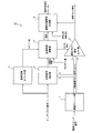
図1は、信号制御回路10の構成を示すブロック図である。信号制御回路10は、遅延チェーン部1、同期信号検出部2、基準信号カウンタ部3、位相制御演算部4、遅延クロック信号セレクト部5および画像先端信号生成部6によって構成される。信号制御回路10は、例えば複写機等に用いられる。
【0015】
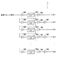
遅延チェーン部1は、図2に示すように、m個のディレイセルDC1〜mと、複数のインバータINVと、により構成され、基準クロック信号を遅延させて同期信号検出部2および遅延クロック信号セレクト部5に出力する。ここで、インバータINVは、基準クロック信号のデューティの崩れを抑制するために挿入される。
【0016】
ディレイセルDC1〜mは、それぞれ入力された入力信号を所定遅延量(例えば、td[psオーダ])だけ遅延させてそれぞれ出力する。つまり、図2に示すように、ディレイセルDC1〜mを多段(直列)に接続し、各ディレイセルに対応する出力段を設けることで、所定遅延量の整数倍(1〜m倍)で遅延させた入力信号を各出力段から出力する。これがmビット幅の信号として、同期信号検出部2および遅延クロック信号セレクト部5に出力される。
【0017】
詳述すると、図2において、1段目のディレイセルDC1は、基準クロック信号を所定遅延量(例えば、td[psオーダ])だけ遅延させて出力する。そして、この出力された信号は、ディレイセルDC1に対応する出力段から遅延信号DL1として同期信号検出部2および遅延クロック信号セレクト部5に出力されると共に、ディレイセルDC2へ出力される。また、2段目のディレイセルDC2は、入力された遅延信号DL1を所定遅延量(例えば、td[psオーダ])だけ遅延させて出力する。そしてこの出力された信号は、ディレイセルDC2に対応する出力段から遅延信号DL2として同期信号検出部2および遅延クロック信号セレクト部5に出力されると共に、ディレイセルDC3へ出力される。
【0018】
同様に、m段目のディレイセルDCmは、入力された遅延信号DLm−1を所定遅延量(例えば、td[psオーダ])だけ遅延させて出力する。そして、この出力された信号は、ディレイセルDCmに対応する出力段から遅延信号DLmとして同期信号検出部2および遅延クロック信号セレクト部5に出力される。ここで遅延チェーン部1は、遅延手段としての機能を有している。また、遅延信号DL1〜mは、遅延基準クロック信号を意味する。
【0019】
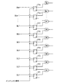
同期信号検出部2は、図3に示すように、m個のDフリップフロップFF1〜m、m個のNAND回路N1〜mおよび演算回路(図示省略)によって構成される。DフリップフロップFF1〜mは、インデックス信号が入力されたタイミングで遅延チェーン部1から入力された遅延信号DL1〜mの状態(“H”または“L”)を検出し、対応するNAND回路N1〜mに出力する。
【0020】
DフリップフロップFF1〜mには、各入力端子Dに遅延チェーン部1から出力された遅延信号DL1〜mが入力され、各クロック端子にインデックス信号が入力される。そして、インデックス信号に同期して各入力端子Dに入力された遅延信号DL1〜mの状態(“H”または“L”)を保持し、保持した値を出力端子Qから出力すると共に、この保持した値を反転させた値を反転出力端子から出力する。
【0021】
そしてNAND回路N1〜mは、前段(ここでは1〜m段)のDフリップフロップの出力端子Qから出力される値と、次段(ここでは2〜m+1段)のDフリップフロップの反転出力端子から出力される値と、をそれぞれ入力し、入力された2つの値の否定論理積を演算し、演算結果を演算回路(図示省略)に出力する。
【0022】
演算回路(図示省略)は、NAND回路N1〜mから出力された演算結果を入力し、基準クロック信号の1周期分の遅延を行うディレイセルの段数を算出する。また、算出したディレイセルの数を位相制御演算部4に出力する。
【0023】
ここで、同期信号検出部2は、第1入力手段および検出手段としての機能を有している。
【0024】
基準信号カウンタ部3は、インデックス信号を入力し、インデックス信号の入力回数を計数する。そして、計数した結果を位相制御演算部4へ出力する。ここで基準信号カウンタ部3は、計数手段としての機能を有している。
【0025】
位相制御演算部4には、同期信号検出部2から出力された基準クロック信号1周期分のディレイセルの段数と、基準信号カウンタ部3から出力されたインデックス信号の計数結果と、外部(例えば、複写機を構成するCPU等)から指示される指示ずらし量と、が入力される。
【0026】
位相制御演算部4は、遅延チェーン部1の出力段番号を選択するセレクト信号を生成し、セレクト信号を遅延クロック信号セレクト部5に出力する。具体的には、例えば、基準クロック信号1周期分のディレイセルがX段、指示ずらし量がZ、予め決められている分解能が1/n、カウント数がKである場合、ずらし段M=X段×1/n×K×Zとして計算する。そして、基準クロック信号と同期した遅延信号を出力するディレイセルの段番号にずらし段Mを加算した値をセレクト信号として出力する。
【0027】
分解能1/nとは、カウント数Kが加算される度に出力されるセレクト信号の値の刻み幅を示している。具体的には、分解能が1/nの時、セレクト信号の値は基準クロック信号1周期分のディレイセルの段数に分解能1/nを乗算した値を刻み幅として変化する。つまり、基準クロック信号1周期分のディレイセルの段数が100段であり、分解能が1/50の時、セレクト信号はカウント数Kが加算される度に、100/50段ずつ、すなわち2段ずつ変化する。また、分解能1/nは予め任意に設定されている固定値であってもいいし、可変値であってもよい。
【0028】
キャリーCとは、ずらし段Mの値が基準クロック信号1周期分のディレイセルの段数以上になる度に1加算されるデータである。キャリーCの値は、位相制御演算部4からキャリー信号として画像先端信号生成部6へ出力される。また、分解能1/nおよびキャリーCは、位相制御演算部4が備えるRAM等で構成される記憶回路に記憶される。
【0029】
ここで位相制御演算部4は、第2入力手段および位相演算手段としての機能を有している。また、指示ずらし量は位相制御信号を意味する。
【0030】
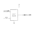
遅延クロック信号セレクト部5は、図4に示すようにセレクト5aを備えて構成される。このセレクト5aには、位相制御演算部4から出力されるセレクト信号と、遅延チェーン部1から出力される遅延信号DL1〜mと、が入力される。そしてセレクト5aは、セレクト信号に応じて、遅延信号DL1〜mの内、一の信号を選択し、選択した信号を画素クロック信号として画像先端信号生成部6と、外部とに出力する。
【0031】
ここで遅延クロック信号セレクト部5は、信号選択手段としての機能を有している。
【0032】
画像先端信号生成部6は、画素クロック信号に同期した画像先端信号を生成する。画像先端信号生成部6には、位相制御演算部4から出力されるキャリー信号と、遅延クロック信号セレクト部5から出力される画素クロック信号と、外部(例えば、複写機を構成するCPU等)から指示される信号生成制御信号と、が入力される。信号生成制御信号とは、画素クロック信号に同期して画像先端信号を生成する際の生成のタイミングを示した信号である。
【0033】
画像先端信号生成部6は、信号生成制御信号に従って画像先端信号を生成するタイミングを決定する。また、更にキャリー信号が1以上の場合には、信号生成制御信号の示した位置に対して、画素クロック信号の周期にキャリー信号の値を乗算した値の位相を変化させたタイミングで画像先端信号を出力する。
【0034】
ここで、画像先端信号生成部6は、信号生成手段としての機能を有している。また、キャリー信号は指示信号を意味する。
【0035】
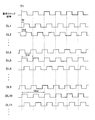
次に図5および6を参照して、本実施の形態における動作を説明する。図5は、遅延チェーン部1に入力される基準クロック信号と、遅延チェーン部1から出力される遅延信号DL1〜11と、のタイミングチャートの一例を示した図である。図5に示すように、遅延信号DL1は、基準クロック信号をディレイセルDC1によって所定遅延量(例えば、td[psオーダ])だけ遅延し、遅延信号DL2は、基準クロック信号をディレイセルDC1および2によって所定遅延量の2倍(つまり、2td[psオーダ])だけ遅延し、遅延信号DL10は、基準クロック信号をディレイセルDC1〜10によって所定遅延量の10倍(つまり、10td[psオーダ])だけ遅延する。
【0036】
また、ここで、遅延信号DL5および10は、基準クロック信号と同期している。つまり、遅延信号DL5および10の遅延量である時間5tdおよび10tdは、基準クロック信号の周期の整数倍であることを意味する。
【0037】
そして遅延チェーン部1は、遅延信号DL1〜mを同期信号検出部2および遅延クロック信号セレクト部5に出力する。同期信号検出部2は、インデックス信号が入力されたタイミングで遅延信号DL1〜mの状態を検出し、基準クロック信号の1周期分にあたるディレイセルの段数を算出する。
【0038】
例えば、図5に示すように、インデックス信号が基準クロック信号の立ち上がりエッジに同期したタイミング(図5に示す時間T1)で同期信号検出部2に入力されたとする。この時間T1において、遅延信号DL1〜3、6、11は“L”になっており、遅延信号DL4、5、9、10は“H”になっている。このように、インデックス信号が入力された時間T1の遅延信号DL1〜mの状態をDフリップフロップFF1〜mが保持して、NAND回路N1〜mに出力する。
【0039】
そして、NAND回路N1〜mは、DフリップフロップFF1〜mから出力された状態に基づいて否定論理積を演算し、演算結果を演算回路(図示省略)に出力する。そして演算回路により、インデックス信号と同期する信号と同期しない信号とが識別される。したがって、図5に示す遅延信号DL5および10(つまり、インデックス信号と同期する信号)に対応するNAND回路N5および10からは“L”が出力され、NAND回路N5および10以外のNAND回路からは“H”が出力される。
【0040】
そして演算回路は、NAND回路N1〜mから出力された値に基づいて、基準クロック信号の1周期分の遅延を行うディレイセルの段数(即ち、NAND回路N10の“10”−NAND回路N5の“5”=5段)を演算して、位相制御演算部4に出力する。
【0041】
基準信号カウンタ部3は、1つの画像データに対して入力されたインデックス信号の入力回数を計数し、計数した結果を位相制御演算部4へ出力する。
【0042】
位相制御演算部4は、同期信号検出部2から出力された基準クロック信号1周期分のディレイセルの段数と、基準信号カウンタ部3から出力されたインデックス信号のカウンタ数と、外部(例えば、複写機を構成するCPU等)から指示ずらし量と、を入力する。入力した値と、分解能1/nおよびキャリーCと、を用いて演算することにより遅延チェーン部1の出力段番号を選択するセレクト信号を生成し、遅延クロック信号セレクト部5へ出力する。
【0043】
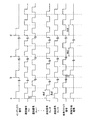
図6は、信号制御回路10に外部から入力されるインデックス信号と、遅延クロック信号セレクト部5に入力される遅延信号と、信号制御回路10から出力される画素クロック信号および画像先端信号と、のタイミングチャートの一例を示した図である。
【0044】
図6において、遅延信号DLi,i+1,・・・,i+4,i+5は遅延クロック信号セレクト部5に入力される遅延信号DL1〜mの一部であり、画素クロック信号は遅延クロック信号セレクト部5から出力された信号である。画像先端信号は、画像先端信号生成部6から出力された信号である。
【0045】
ここで、説明のため、遅延チェーン部1のディレイセル1段による遅延量はtdとし、基準クロック信号の1周期分のディレイセルが5段である場合を一例として図示している。更に分解能1/5、指示ずらし量Z=iとし、カウント数KおよびキャリーCは初期値をゼロとして説明する。
【0046】
図6において、タイミングaで1回目のインデックス信号が入力されることにより、遅延クロック信号セレクト部5はセレクト信号によって遅延信号DLiを選択し、該信号を画素クロック信号として出力する。そして、画像先端信号生成部6は画素クロック信号に同期して画像先端信号を出力する。
【0047】
続いて、タイミングbで2回目のインデックス信号が入力されると、遅延クロック信号セレクト部5はセレクト信号によって遅延信号DLi+1を選択し、該信号を画素クロック信号として出力する。そして、画像先端信号生成部6は画素クロック信号に同期して画像先端信号を出力する。この時、画像先端信号はインデックス信号の立ち上がりエッジに対して、時間td’ほど遅れて出力されることになる。
【0048】
次に、タイミングcで5回目のインデックス信号が入力されると、遅延クロック信号セレクト部5はセレクト信号によって遅延信号DLi+4を選択し、該信号を画素クロック信号として出力する。そして、画像先端信号生成部6は画素クロック信号に同期して画像先端信号を生成する。この時、画像先端信号はインデックス信号の立ち上がりエッジに対して、時間4td’ほど遅れて出力されることになる。
【0049】
続いて、タイミングdで6回目のインデックス信号が入力されると、位相制御演算部4において演算されるずらし段Mが、基準クロック信号1周期分のディレイセルの段数(図6においては“5”)を超えるため、キャリーCを“1”としてずらし段Mを演算し、セレクト信号を出力する。したがって、遅延クロック信号セレクト部5はセレクト信号によって遅延信号DLiを選択し、該信号を画素クロック信号として出力する。そして、画像先端信号生成部6は画素クロック信号に対して1周期遅れたタイミングで画像先端信号を生成する。この時、画像先端信号はインデックス信号の立ち上がりエッジに対して、時間5td’ほど遅れて出力されることになる。
【0050】
尚、画像先端信号生成部6が画像先端信号を出力する画素クロック信号に同期したタイミングは、外部(例えば、複写機を構成するCPU等)から入力される信号生成制御信号によって任意に設定可能である。また、インデックス信号が外部から入力される度に遅延クロック信号セレクト部5によって切り替えられた画素クロック信号が出力されるが、安定した画素クロック信号を用いるために、画像先端信号は遅延クロック信号セレクト部5を出力して所定周期経過後の画素クロック信号に同期して生成される。
【0051】
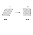
このように、信号制御回路10は、基準クロック信号に対して位相をずらした信号を画素クロック信号として出力し、更に該画素クロック信号に同期して画像先端信号を出力することにより、画像の各行の先頭の書き出し位置を制御することができる。即ち、図7に示すように、複写機等の画像形成装置によって補正前は傾いて出力されていた画像71を、信号制御回路10を用いて画像の各行の先頭の書き出し位置を示す画像先端信号を制御することにより、画像72のように傾きを補正してまっすぐに出力することができる。
【0052】
更に、画像先端信号生成部6に入力される信号生成制御信号によって、画像先端信号を出力するタイミングは任意に設定可能であるから、画像の各行の先頭の書き出し位置も任意に制御することができる。つまり、画像の各行の先端の書き出し位置のずらす量を任意に設定することができる。
【0053】
以上のように、本実施の形態の信号制御回路10によれば、遅延チェーン部1で基準クロック信号から所定遅延量を遅延させた遅延信号をmビット出力し、同期信号検出部2で基準クロック信号の1周期分の遅延を行うために必要となるディレイセルの段数を検出する。そして位相制御演算部4は、同期信号検出部2によって算出されたディレイセルの段数と、基準信号カウンタ部3から入力されるインデックス信号のカウンタ数と、外部(例えば、複写機を構成するCPU等)から入力される指示ずらし量Zと、分解能1/nと、に基づいて、ずらし段Mを演算する。更にずらし段Mに基づいてセレクト信号を生成し、セレクト信号を遅延クロック信号セレクト部5に出力する。
【0054】
遅延クロック信号セレクト部5は、入力されたセレクト信号に応じて、遅延チェーン部1が出力する遅延信号の内、一の信号を選択し、選択した信号を画素クロック信号として外部に出力すると共に、画像先端信号生成部6に出力する。
【0055】
画像先端信号生成部6は、外部(例えば、複写機を構成するCPU等)から入力される信号生成制御信号に応じて、入力された画素クロック信号に同期した信号を生成し、画像先端信号として外部に出力する。
【0056】
したがって、信号生成回路10は、基準クロック信号の1周期/nの時間を遅延させた遅延信号を生成し、外部から入力されたインデックス信号に対して任意のずらし量を遅延させた遅延信号を画素クロック信号として出力する。これにより、画素クロック信号のタイミングを高精度で制御できるため、画像の傾き(歪み)も高精度で補正することができる。
【0057】
更に、画像先端信号は画素クロック信号に同期したタイミングで生成するが、外部(例えば、複写機を構成するCPU等)から入力される信号生成制御信号によって画像先端信号を生成するタイミングを制御することができる。このため、信号生成制御信号を任意に設定することにより、画像の各行の先頭の書き出し位置を任意に制御できる。
【0058】
分解能1/nおよび信号生成制御信号の値は、複写機等の画像形成装置の温度変化による書き込みユニットおよび読み取りユニットのレンズ特性の変化、装置組み立て時の製造誤差、各製品の製造バラツキ等にしたがって予め設定され、画像形成装置に含まれる記憶回路等に記憶されて出荷される。そして複写機等で画像を形成する際に、信号制御回路10によって画像の各行の先端の書き出し位置が制御されることにより、画像の傾き(歪み)が補正されて出力される。
【0059】
また、集積回路(デジタル回路)内に信号制御回路10を構成すれば、信号制御回路10は高精度の遅延を実現でき、信号制御回路10を安価に提供できる。
【0060】
なお、本発明は、上記実施の形態の内容に限定されるものではなく、本発明の趣旨を逸脱しない範囲で適宜変更可能であり、例えば、画像のより複雑な補正を実現するために、位相制御演算部4におけるずらし段Mの演算式として、“ずらし段M=X段×1/n×K×Z”を一例として挙げて説明したが、これに限定されるものではなく、二次関数等を含む演算式としてもよい。これにより、画像に対してより複雑な補正が可能となる。また、分解能1/nは、外部(例えば、複写機を構成するCPU等)から入力される値であってもよい。これにより、分解能1/nを小さな値に設定した場合、画像を更に細かく補正することが可能となる。更に、本実施の形態において、ずらし段Mは1インデックス信号毎に加算されるものとして説明したが、複数のインデックス信号毎にずらし段Mを加算してもよい。また、インデックス信号によってずらし段Mの値が異なってもよく、ずらし段Mは位相制御演算部6においてインデックス信号の入力毎に任意に設定することが可能である。
【0061】
【発明の効果】
請求項1記載の発明によれば、例えば、パルス信号やステップ信号等の所定信号と同期する遅延基準クロック信号に基づいて基準クロック信号の1周期分に係る遅延素子の段数を検出し、この段数、計数量、位相制御信号及び遅延手段を選択するための選択信号の刻み幅を示す分解能を積載した積算情報を演算する。そして、この積算情報に基づいて、選択信号を生成し、当該生成された選択信号に基づいて、遅延基準クロック信号の中から択一的に選択した信号を外部出力する。これにより、遅延基準クロック信号のタイミングを基準クロック信号の1周期以下の時間で制御でき、高精度な制御を実現できる。
【0063】
請求項2記載の発明によれば、画像先端信号に基づいたタイミングで、信号選択手段から出力された信号に同期した信号を生成する。これにより、画像の各行の先端の書き出し位置を高精度で制御できる。
【0065】
請求項3記載の発明によれば、画像先端信号生成手段は、指示信号に基づいて画像先端信号を生成する。これにより、画像の傾き等を補正して出力することができる。
【図面の簡単な説明】
【図1】信号制御回路の構成を示すブロック図。
【図2】遅延チェーン部の回路構成を示す図。
【図3】同期信号検出部が備える検出回路の回路構成を示す図。
【図4】遅延クロック信号セレクト部が備えるセレクトを示す図。
【図5】基準クロック信号と、遅延チェーン部から出力される遅延信号と、を示すタイミングチャート。
【図6】インデックス信号と、遅延信号と、画素クロック信号と、画像先端信号と、を示すタイミングチャート。
【図7】信号制御回路10による補正前後の画像を示す図。
【符号の説明】
1 遅延チェーン部
2 同期信号検出部
3 基準信号カウンタ部
4 位相制御演算部
5 遅延クロック信号セレクト部
6 画像先端信号生成部[0001]
BACKGROUND OF THE INVENTION
The present invention relates to an image forming apparatus .
[0002]
[Prior art]
An image forming apparatus such as a copying machine forms a read image or image at the time of image reading or writing due to a change in lens characteristics of a writing unit and a reading unit due to a temperature change, a manufacturing error at the time of assembling the device, a manufacturing variation of each product, The image sometimes tilted (distorted). Therefore, when forming an image, the image data is processed in units of pixels, and correction processing is performed so that the image is formed straight.
[0003]
[Problems to be solved by the invention]
However, such processing of image data has an effect on image processing such as error diffusion, which may cause moiré and the like, causing image quality degradation and the like. On the other hand, in an image forming apparatus such as a copying machine, one image is output line by line in the main scanning direction, and an image is formed by repeating this in the sub scanning direction.
[0004]
Accordingly, an object of the present invention is to provide a circuit that corrects an image with high accuracy by controlling the writing start position of each line of the image with a resolution equal to or less than the cycle of the reference clock.
[0005]
[Means for Solving the Problems]
In order to solve the above problems, the invention described in
Delay means for delaying a reference clock signal by a plurality of delay elements connected in multiple stages and outputting the delayed reference clock signal for each stage, and based on a delayed reference clock signal synchronized with a predetermined signal, Detecting means for detecting the number of stages of the delay elements for one cycle;
Counting means for counting the predetermined signal;
The integrated information obtained by integrating the number of stages detected by the detecting means, the count amount counted by the counting means , the phase control signal, and the resolution indicating the step width of the selection signal for selecting the delay means is calculated, and the calculation is performed. A signal for generating a pixel clock signal by generating the selection signal based on the accumulated information and selecting a signal alternatively from the delayed reference clock signal based on the generated selection signal A selection means;
And an image leading edge signal generating means for generating and outputting an image leading edge signal synchronized with the pixel clock signal.
[0006]
According to the first aspect of the present invention, for example, the number of stages of the delay elements corresponding to one cycle of the reference clock signal is detected based on the delay reference clock signal synchronized with a predetermined signal such as a pulse signal or a step signal. The integrated information loaded with the resolution indicating the step size of the selection signal for selecting the number of stages , the count amount , the phase control signal, and the delay means is calculated. Then, a selection signal is generated based on the integration information, and a signal that is alternatively selected from the delay reference clock signals is output to the outside based on the generated selection signal . As a result, the timing of the delayed reference clock signal can be controlled within a period of one cycle or less of the reference clock signal, and high-precision control can be realized.
[0008]
The invention according to
The start writing position of each line of the image is controlled according to the image leading edge signal .
[0009]
According to the second aspect of the present invention, a signal synchronized with the signal output from the signal selection means is generated at a timing based on the image leading edge signal . Thereby, it is possible to control the writing position of the leading edge of each line of the image with high accuracy.
[0011]
The invention according to claim 3 is the image forming apparatus according to
The signal selection means outputs an instruction signal for changing the phase of the image leading edge signal when the integration information exceeds the period of the reference clock signal,
The image leading edge signal generating means generates the image leading edge signal based on the instruction signal .
[0012]
According to the third aspect of the present invention, the image leading edge signal generating means generates the image leading edge signal based on the instruction signal. Thereby, it is possible to correct and output the inclination of the image.
[0013]
DETAILED DESCRIPTION OF THE INVENTION
Hereinafter, embodiments of the
[0014]
FIG. 1 is a block diagram showing the configuration of the
[0015]
As shown in FIG. 2, the
[0016]
Each of the delay cells DC1 to DCm outputs the input signal after delaying the input signal by a predetermined delay amount (for example, td [ps order]). That is, as shown in FIG. 2, delay cells DC1 to DCm are connected in multiple stages (in series), and an output stage corresponding to each delay cell is provided, thereby delaying by an integral multiple (1 to m times) of a predetermined delay amount. The input signal is output from each output stage. This is output to the
[0017]
More specifically, in FIG. 2, the first-stage delay cell DC1 delays the reference clock signal by a predetermined delay amount (for example, td [ps order]) and outputs the delayed signal. The output signal is output from the output stage corresponding to the delay cell DC1 to the synchronization
[0018]
Similarly, the m-th delay cell DCm delays the input delay signal DLm−1 by a predetermined delay amount (for example, td [ps order]) and outputs it. This output signal is output from the output stage corresponding to the delay cell DCm to the synchronization
[0019]
As shown in FIG. 3, the synchronization
[0020]
In the D flip-flops FF1 to FFm, the delay signals DL1 to m output from the
[0021]
The NAND circuits N1 to N1m have a value output from the output terminal Q of the preceding stage (here 1 to m stages) D flip-flop and an inverted output terminal of the next stage (here 2 to m + 1 stages) D flip-flop. And the value output from each of the two values are input, the logical product of the two input values is calculated, and the calculation result is output to a calculation circuit (not shown).
[0022]
An arithmetic circuit (not shown) receives the arithmetic results output from the NAND circuits N1 to Nm, and calculates the number of stages of delay cells that perform a delay of one cycle of the reference clock signal. Further, the calculated number of delay cells is output to the phase
[0023]
Here, the synchronization
[0024]
The reference signal counter unit 3 receives an index signal and counts the number of times the index signal is input. Then, the counted result is output to the phase
[0025]
The phase
[0026]
The phase
[0027]
The
[0028]
Carry C is data that is incremented by one whenever the value of shift stage M becomes equal to or greater than the number of delay cell stages for one cycle of the reference clock signal. The value of carry C is output from the phase
[0029]
Here, the phase
[0030]
The delayed
[0031]
Here, the delayed
[0032]
The image leading edge signal generation unit 6 generates an image leading edge signal synchronized with the pixel clock signal. The image leading edge signal generation unit 6 includes a carry signal output from the phase
[0033]
The image leading edge signal generator 6 determines the timing for generating the image leading edge signal in accordance with the signal generation control signal. Further, when the carry signal is 1 or more, the image leading edge signal is changed at the timing when the phase of the value obtained by multiplying the cycle of the pixel clock signal by the value of the carry signal is changed with respect to the position indicated by the signal generation control signal. Is output.
[0034]
Here, the image leading edge signal generation unit 6 has a function as signal generation means. The carry signal means an instruction signal.
[0035]
Next, operations in the present embodiment will be described with reference to FIGS. FIG. 5 is a diagram illustrating an example of a timing chart of the reference clock signal input to the
[0036]
Here, the delay signals DL5 and 10 are synchronized with the reference clock signal. That is, it means that the times 5td and 10td, which are the delay amounts of the delay signals DL5 and 10, are an integral multiple of the period of the reference clock signal.
[0037]
Then, the
[0038]
For example, as shown in FIG. 5, it is assumed that the index signal is input to the synchronization
[0039]
Then, the NAND circuits N1 to Nm calculate a negative logical product based on the states output from the D flip-flops FF1 to FFm, and output the calculation result to an arithmetic circuit (not shown). Then, a signal that is synchronized with the index signal and a signal that is not synchronized are identified by the arithmetic circuit. Therefore, “L” is output from NAND circuits N5 and N corresponding to delay signals DL5 and DL (that is, a signal synchronized with the index signal) shown in FIG. 5, and “N” is output from NAND circuits other than NAND circuits N5 and N10. H "is output.
[0040]
Then, based on the values output from the NAND circuits N1 to Nm, the arithmetic circuit determines the number of delay cell stages for delaying one cycle of the reference clock signal (ie, “10” of the NAND circuit N10— “ 5 ″ = 5 stages) and output to the phase
[0041]
The reference signal counter unit 3 counts the number of times the index signal is input for one image data, and outputs the counted result to the phase
[0042]
The phase
[0043]
6 shows an index signal input from the outside to the
[0044]
In FIG. 6, delay signals DLi, i + 1,..., I + 4, i + 5 are part of the
[0045]
Here, for the sake of explanation, the delay amount by one stage of the delay cells of the
[0046]
In FIG. 6, when the first index signal is input at timing a, the delayed
[0047]
Subsequently, when the second index signal is input at timing b, the delayed
[0048]
Next, when the fifth index signal is input at timing c, the delayed
[0049]
Subsequently, when the sixth index signal is input at timing d, the shift stage M calculated in the phase
[0050]
The timing at which the image leading edge signal generation unit 6 synchronizes with the pixel clock signal that outputs the image leading edge signal can be arbitrarily set by a signal generation control signal input from the outside (for example, a CPU constituting the copying machine). is there. Also, every time an index signal is input from the outside, a pixel clock signal switched by the delay
[0051]
As described above, the
[0052]
Furthermore, since the timing for outputting the image leading edge signal can be arbitrarily set by the signal generation control signal input to the image leading edge signal generating unit 6, the leading writing position of each line of the image can also be arbitrarily controlled. . That is, it is possible to arbitrarily set the shift amount of the writing position at the tip of each line of the image.
[0053]
As described above, according to the
[0054]
The delay clock
[0055]
The image leading edge signal generator 6 generates a signal synchronized with the input pixel clock signal in accordance with a signal generation control signal input from the outside (for example, a CPU constituting the copying machine), and serves as an image leading edge signal. Output to the outside.
[0056]
Therefore, the
[0057]
Furthermore, the image leading edge signal is generated at a timing synchronized with the pixel clock signal, but the timing for generating the image leading edge signal is controlled by a signal generation control signal input from the outside (for example, a CPU constituting the copying machine). Can do. Therefore, by arbitrarily setting the signal generation control signal, it is possible to arbitrarily control the start writing position of each line of the image.
[0058]
The
[0059]
Further, if the
[0060]
Note that the present invention is not limited to the contents of the above-described embodiment, and can be appropriately changed without departing from the spirit of the present invention. For example, in order to realize more complicated correction of an image, the phase As an arithmetic expression of the shift stage M in the
[0061]
【The invention's effect】
According to the first aspect of the present invention, for example, the number of stages of the delay elements corresponding to one period of the reference clock signal is detected based on the delay reference clock signal synchronized with a predetermined signal such as a pulse signal or a step signal, and the number of stages The integrated information loaded with the resolution indicating the increment of the selection signal for selecting the count amount , the phase control signal, and the delay means is calculated. Then, a selection signal is generated based on the integration information, and a signal that is alternatively selected from the delay reference clock signals is output to the outside based on the generated selection signal . As a result, the timing of the delayed reference clock signal can be controlled within a period of one cycle or less of the reference clock signal, and high-precision control can be realized.
[0063]
According to the second aspect of the present invention, a signal synchronized with the signal output from the signal selection means is generated at a timing based on the image leading edge signal . Thereby, it is possible to control the writing position of the leading edge of each line of the image with high accuracy.
[0065]
According to the invention described in claim 3, the image leading edge signal generating means generates the image leading edge signal based on the instruction signal. Thereby, it is possible to correct and output the inclination of the image.
[Brief description of the drawings]
FIG. 1 is a block diagram illustrating a configuration of a signal control circuit.
FIG. 2 is a diagram showing a circuit configuration of a delay chain unit.
FIG. 3 is a diagram illustrating a circuit configuration of a detection circuit included in a synchronization signal detection unit.
FIG. 4 is a diagram showing a selection included in a delayed clock signal selection unit.
FIG. 5 is a timing chart showing a reference clock signal and a delay signal output from a delay chain unit.
FIG. 6 is a timing chart showing an index signal, a delay signal, a pixel clock signal, and an image leading edge signal.
7 is a diagram showing images before and after correction by the
[Explanation of symbols]
DESCRIPTION OF
Claims (3)
前記所定信号を計数する計数手段と、
前記検出手段により検出された段数、前記計数手段により計数された計数量、位相制御信号及び前記遅延手段を選択するための選択信号の刻み幅を示す分解能を積算した積算情報を演算し、当該演算された積算情報に基づいて、前記選択信号を生成し、当該生成された選択信号に基づいて、前記遅延基準クロック信号の中から択一的に信号を選択することにより画素クロック信号を出力する信号選択手段と、
前記画素クロック信号に同期した画像先端信号を生成し、出力する画像先端信号生成手段と、
を有することを特徴とする画像形成装置。Delay means for delaying a reference clock signal by a plurality of delay elements connected in multiple stages and outputting the delayed reference clock signal for each stage, and based on a delayed reference clock signal synchronized with a predetermined signal, Detecting means for detecting the number of stages of the delay elements for one cycle;
Counting means for counting the predetermined signal;
The integrated information obtained by integrating the number of stages detected by the detecting means, the count amount counted by the counting means , the phase control signal, and the resolution indicating the step width of the selection signal for selecting the delay means is calculated, and the calculation is performed. A signal for generating a pixel clock signal by generating the selection signal based on the accumulated information and selecting a signal alternatively from the delayed reference clock signal based on the generated selection signal A selection means;
An image leading edge signal generating means for generating and outputting an image leading edge signal synchronized with the pixel clock signal;
An image forming apparatus comprising:
前記画像先端信号生成手段は、前記指示信号に基づいて前記画像先端信号を生成することを特徴とする請求項1または請求項2に記載の画像形成装置。The signal selection means outputs an instruction signal for changing the phase of the image leading edge signal when the integration information exceeds the period of the reference clock signal,
The image leading edge signal generating means, the image forming apparatus according to claim 1 or claim 2, characterized in that to generate the image leading edge signal based on the instruction signal.
Priority Applications (2)
| Application Number | Priority Date | Filing Date | Title |
|---|---|---|---|
| JP2002072081A JP4200682B2 (en) | 2002-03-15 | 2002-03-15 | Image forming apparatus |
| US10/383,048 US7110017B2 (en) | 2002-03-15 | 2003-03-06 | Signal controlling circuit |
Applications Claiming Priority (1)
| Application Number | Priority Date | Filing Date | Title |
|---|---|---|---|
| JP2002072081A JP4200682B2 (en) | 2002-03-15 | 2002-03-15 | Image forming apparatus |
Publications (3)
| Publication Number | Publication Date |
|---|---|
| JP2003266760A JP2003266760A (en) | 2003-09-24 |
| JP2003266760A5 JP2003266760A5 (en) | 2005-08-11 |
| JP4200682B2 true JP4200682B2 (en) | 2008-12-24 |
Family
ID=28035153
Family Applications (1)
| Application Number | Title | Priority Date | Filing Date |
|---|---|---|---|
| JP2002072081A Expired - Fee Related JP4200682B2 (en) | 2002-03-15 | 2002-03-15 | Image forming apparatus |
Country Status (2)
| Country | Link |
|---|---|
| US (1) | US7110017B2 (en) |
| JP (1) | JP4200682B2 (en) |
Families Citing this family (4)
| Publication number | Priority date | Publication date | Assignee | Title |
|---|---|---|---|---|
| FR2871963B1 (en) * | 2004-06-22 | 2006-09-15 | Thales Sa | ELECTRONIC DEVICE FOR GENERATING SYNCHRONIZATION SIGNALS |
| US8014692B2 (en) * | 2006-04-19 | 2011-09-06 | Kyocera Mita Corporation | Image forming apparatus |
| GB2560086B (en) * | 2015-09-09 | 2020-02-05 | Imagination Tech Ltd | Synchronising devices |
| CN116155246A (en) * | 2022-12-12 | 2023-05-23 | 天津兆讯电子技术有限公司 | High-precision delay clock generation circuit and chip |
Family Cites Families (4)
| Publication number | Priority date | Publication date | Assignee | Title |
|---|---|---|---|---|
| JPH0795155B2 (en) * | 1987-09-18 | 1995-10-11 | 富士写真フイルム株式会社 | Optical scanning device synchronization circuit |
| JP2667590B2 (en) * | 1991-03-12 | 1997-10-27 | 三田工業株式会社 | Horizontal synchronizing signal generator for image forming apparatus using laser beam |
| US5760816A (en) * | 1996-02-06 | 1998-06-02 | Hewlett-Packard Company | Variable phase clock generator for an electrophotographic printer |
| US6154292A (en) * | 1997-02-14 | 2000-11-28 | Konica Corporation | Multi-beam scanning method and control apparatus for the same |
-
2002
- 2002-03-15 JP JP2002072081A patent/JP4200682B2/en not_active Expired - Fee Related
-
2003
- 2003-03-06 US US10/383,048 patent/US7110017B2/en active Active
Also Published As
| Publication number | Publication date |
|---|---|
| US20030177410A1 (en) | 2003-09-18 |
| US7110017B2 (en) | 2006-09-19 |
| JP2003266760A (en) | 2003-09-24 |
Similar Documents
| Publication | Publication Date | Title |
|---|---|---|
| US10491201B2 (en) | Delay circuit, count value generation circuit, and physical quantity sensor | |
| JP2010114875A (en) | Duty detecting circuit and duty correcting circuit including the same | |
| US6917660B2 (en) | Adaptive de-skew clock generation | |
| JP2907033B2 (en) | Timing signal generator | |
| JP4200682B2 (en) | Image forming apparatus | |
| JP5001606B2 (en) | Timing detection circuit | |
| US20170054365A1 (en) | PWM Signal Generator and Switching Power Supply Device Having Same | |
| JP4016034B2 (en) | Pulse width measuring device with auto range setting function | |
| JP2008172574A (en) | Clock phase shift circuit | |
| US8008958B2 (en) | Electronic device and method of correcting clock signal deviations in an electronic device | |
| US7782109B2 (en) | Delay circuit and related method | |
| JP2002141786A (en) | Device and its operating method | |
| JP3770378B2 (en) | Phase comparison circuit | |
| JPH05216558A (en) | Timer circuit | |
| JP5190472B2 (en) | Driving circuit | |
| JP4886900B2 (en) | Electrical circuit and signal processing method | |
| JP4819493B2 (en) | Circuit system | |
| JP3760822B2 (en) | Signal control circuit and image forming apparatus | |
| JP2861901B2 (en) | Clock phase synchronization circuit | |
| JP5439964B2 (en) | Delay comparison circuit, delay comparison method, delay circuit, and semiconductor integrated circuit | |
| JP4189729B2 (en) | Asynchronous readout method of timer count value and timer | |
| JP2008040691A (en) | Clock duty automatic correction circuit and clock duty automatic correction method using the same | |
| JP2651300B2 (en) | Timer circuit | |
| JPH0636028A (en) | Histogram generating device | |
| JP3311555B2 (en) | Image memory readout circuit |
Legal Events
| Date | Code | Title | Description |
|---|---|---|---|
| A521 | Request for written amendment filed |
Free format text: JAPANESE INTERMEDIATE CODE: A523 Effective date: 20050126 |
|
| A621 | Written request for application examination |
Free format text: JAPANESE INTERMEDIATE CODE: A621 Effective date: 20050126 |
|
| A977 | Report on retrieval |
Free format text: JAPANESE INTERMEDIATE CODE: A971007 Effective date: 20070806 |
|
| A131 | Notification of reasons for refusal |
Free format text: JAPANESE INTERMEDIATE CODE: A131 Effective date: 20070814 |
|
| A521 | Request for written amendment filed |
Free format text: JAPANESE INTERMEDIATE CODE: A523 Effective date: 20071012 |
|
| A131 | Notification of reasons for refusal |
Free format text: JAPANESE INTERMEDIATE CODE: A131 Effective date: 20080311 |
|
| A521 | Request for written amendment filed |
Free format text: JAPANESE INTERMEDIATE CODE: A523 Effective date: 20080512 |
|
| TRDD | Decision of grant or rejection written | ||
| A01 | Written decision to grant a patent or to grant a registration (utility model) |
Free format text: JAPANESE INTERMEDIATE CODE: A01 Effective date: 20080916 |
|
| A01 | Written decision to grant a patent or to grant a registration (utility model) |
Free format text: JAPANESE INTERMEDIATE CODE: A01 |
|
| A61 | First payment of annual fees (during grant procedure) |
Free format text: JAPANESE INTERMEDIATE CODE: A61 Effective date: 20080929 |
|
| R150 | Certificate of patent or registration of utility model |
Ref document number: 4200682 Country of ref document: JP Free format text: JAPANESE INTERMEDIATE CODE: R150 Free format text: JAPANESE INTERMEDIATE CODE: R150 |
|
| FPAY | Renewal fee payment (event date is renewal date of database) |
Free format text: PAYMENT UNTIL: 20111017 Year of fee payment: 3 |
|
| FPAY | Renewal fee payment (event date is renewal date of database) |
Free format text: PAYMENT UNTIL: 20121017 Year of fee payment: 4 |
|
| FPAY | Renewal fee payment (event date is renewal date of database) |
Free format text: PAYMENT UNTIL: 20121017 Year of fee payment: 4 |
|
| FPAY | Renewal fee payment (event date is renewal date of database) |
Free format text: PAYMENT UNTIL: 20131017 Year of fee payment: 5 |
|
| S531 | Written request for registration of change of domicile |
Free format text: JAPANESE INTERMEDIATE CODE: R313531 |
|
| S533 | Written request for registration of change of name |
Free format text: JAPANESE INTERMEDIATE CODE: R313533 |
|
| R350 | Written notification of registration of transfer |
Free format text: JAPANESE INTERMEDIATE CODE: R350 |
|
| LAPS | Cancellation because of no payment of annual fees |