JP4199708B2 - 回折光学素子及び回折光学素子を形成する方法 - Google Patents
回折光学素子及び回折光学素子を形成する方法 Download PDFInfo
- Publication number
- JP4199708B2 JP4199708B2 JP2004217818A JP2004217818A JP4199708B2 JP 4199708 B2 JP4199708 B2 JP 4199708B2 JP 2004217818 A JP2004217818 A JP 2004217818A JP 2004217818 A JP2004217818 A JP 2004217818A JP 4199708 B2 JP4199708 B2 JP 4199708B2
- Authority
- JP
- Japan
- Prior art keywords
- substrate
- layer
- light
- resist layer
- forming
- Prior art date
- Legal status (The legal status is an assumption and is not a legal conclusion. Google has not performed a legal analysis and makes no representation as to the accuracy of the status listed.)
- Expired - Fee Related
Links
- 238000000034 method Methods 0.000 title claims description 35
- 230000003287 optical effect Effects 0.000 title claims description 17
- 239000000758 substrate Substances 0.000 claims description 47
- 239000000463 material Substances 0.000 claims description 25
- VYPSYNLAJGMNEJ-UHFFFAOYSA-N Silicium dioxide Chemical compound O=[Si]=O VYPSYNLAJGMNEJ-UHFFFAOYSA-N 0.000 claims description 15
- 238000005530 etching Methods 0.000 claims description 11
- 239000000377 silicon dioxide Substances 0.000 claims description 7
- WUKWITHWXAAZEY-UHFFFAOYSA-L calcium difluoride Chemical compound [F-].[F-].[Ca+2] WUKWITHWXAAZEY-UHFFFAOYSA-L 0.000 claims description 6
- OYLGJCQECKOTOL-UHFFFAOYSA-L barium fluoride Chemical compound [F-].[F-].[Ba+2] OYLGJCQECKOTOL-UHFFFAOYSA-L 0.000 claims description 5
- 229910001632 barium fluoride Inorganic materials 0.000 claims description 5
- 235000012239 silicon dioxide Nutrition 0.000 claims description 5
- 229910001634 calcium fluoride Inorganic materials 0.000 claims description 4
- 238000005498 polishing Methods 0.000 claims description 3
- 235000012431 wafers Nutrition 0.000 description 19
- 238000004519 manufacturing process Methods 0.000 description 14
- 238000005286 illumination Methods 0.000 description 9
- 238000001459 lithography Methods 0.000 description 9
- 239000004065 semiconductor Substances 0.000 description 6
- 238000000059 patterning Methods 0.000 description 5
- 230000005540 biological transmission Effects 0.000 description 4
- 230000015572 biosynthetic process Effects 0.000 description 4
- 238000000151 deposition Methods 0.000 description 4
- 229910016036 BaF 2 Inorganic materials 0.000 description 2
- 229910004298 SiO 2 Inorganic materials 0.000 description 2
- 238000005229 chemical vapour deposition Methods 0.000 description 2
- 230000000694 effects Effects 0.000 description 2
- 230000008020 evaporation Effects 0.000 description 2
- 238000001704 evaporation Methods 0.000 description 2
- 238000003384 imaging method Methods 0.000 description 2
- 238000004544 sputter deposition Methods 0.000 description 2
- 238000010521 absorption reaction Methods 0.000 description 1
- 239000005350 fused silica glass Substances 0.000 description 1
- 239000011521 glass Substances 0.000 description 1
- 150000002500 ions Chemical class 0.000 description 1
- 239000004973 liquid crystal related substance Substances 0.000 description 1
- 239000000203 mixture Substances 0.000 description 1
- 238000000206 photolithography Methods 0.000 description 1
- 229920002120 photoresistant polymer Polymers 0.000 description 1
- 238000012795 verification Methods 0.000 description 1
Images


Classifications
-
- G—PHYSICS
- G03—PHOTOGRAPHY; CINEMATOGRAPHY; ANALOGOUS TECHNIQUES USING WAVES OTHER THAN OPTICAL WAVES; ELECTROGRAPHY; HOLOGRAPHY
- G03F—PHOTOMECHANICAL PRODUCTION OF TEXTURED OR PATTERNED SURFACES, e.g. FOR PRINTING, FOR PROCESSING OF SEMICONDUCTOR DEVICES; MATERIALS THEREFOR; ORIGINALS THEREFOR; APPARATUS SPECIALLY ADAPTED THEREFOR
- G03F7/00—Photomechanical, e.g. photolithographic, production of textured or patterned surfaces, e.g. printing surfaces; Materials therefor, e.g. comprising photoresists; Apparatus specially adapted therefor
- G03F7/70—Microphotolithographic exposure; Apparatus therefor
- G03F7/70058—Mask illumination systems
- G03F7/7015—Details of optical elements
- G03F7/70158—Diffractive optical elements
-
- G—PHYSICS
- G02—OPTICS
- G02B—OPTICAL ELEMENTS, SYSTEMS OR APPARATUS
- G02B27/00—Optical systems or apparatus not provided for by any of the groups G02B1/00 - G02B26/00, G02B30/00
- G02B27/0025—Optical systems or apparatus not provided for by any of the groups G02B1/00 - G02B26/00, G02B30/00 for optical correction, e.g. distorsion, aberration
- G02B27/0037—Optical systems or apparatus not provided for by any of the groups G02B1/00 - G02B26/00, G02B30/00 for optical correction, e.g. distorsion, aberration with diffracting elements
- G02B27/0043—Optical systems or apparatus not provided for by any of the groups G02B1/00 - G02B26/00, G02B30/00 for optical correction, e.g. distorsion, aberration with diffracting elements in projection exposure systems, e.g. microlithographic systems
-
- G—PHYSICS
- G02—OPTICS
- G02B—OPTICAL ELEMENTS, SYSTEMS OR APPARATUS
- G02B5/00—Optical elements other than lenses
- G02B5/18—Diffraction gratings
- G02B5/1838—Diffraction gratings for use with ultraviolet radiation or X-rays
-
- G—PHYSICS
- G02—OPTICS
- G02B—OPTICAL ELEMENTS, SYSTEMS OR APPARATUS
- G02B5/00—Optical elements other than lenses
- G02B5/18—Diffraction gratings
- G02B5/1847—Manufacturing methods
- G02B5/1857—Manufacturing methods using exposure or etching means, e.g. holography, photolithography, exposure to electron or ion beams
-
- G—PHYSICS
- G03—PHOTOGRAPHY; CINEMATOGRAPHY; ANALOGOUS TECHNIQUES USING WAVES OTHER THAN OPTICAL WAVES; ELECTROGRAPHY; HOLOGRAPHY
- G03F—PHOTOMECHANICAL PRODUCTION OF TEXTURED OR PATTERNED SURFACES, e.g. FOR PRINTING, FOR PROCESSING OF SEMICONDUCTOR DEVICES; MATERIALS THEREFOR; ORIGINALS THEREFOR; APPARATUS SPECIALLY ADAPTED THEREFOR
- G03F7/00—Photomechanical, e.g. photolithographic, production of textured or patterned surfaces, e.g. printing surfaces; Materials therefor, e.g. comprising photoresists; Apparatus specially adapted therefor
- G03F7/70—Microphotolithographic exposure; Apparatus therefor
- G03F7/70216—Mask projection systems
- G03F7/70316—Details of optical elements, e.g. of Bragg reflectors, extreme ultraviolet [EUV] multilayer or bilayer mirrors or diffractive optical elements
Landscapes
- Physics & Mathematics (AREA)
- General Physics & Mathematics (AREA)
- Optics & Photonics (AREA)
- Health & Medical Sciences (AREA)
- Toxicology (AREA)
- Engineering & Computer Science (AREA)
- Manufacturing & Machinery (AREA)
- Diffracting Gratings Or Hologram Optical Elements (AREA)
- Exposure And Positioning Against Photoresist Photosensitive Materials (AREA)
- Exposure Of Semiconductors, Excluding Electron Or Ion Beam Exposure (AREA)
Description
具体的な構成及び配列が説明されるが、この説明は例示目的のためにのみ行われることが理解されるべきである。当業者は、本発明の思想及び範囲から逸脱することなくその他の構成及び配列を使用することができることを認識するであろう。本発明をその他の様々な用途において使用することもできることが当業者に明らかになるであろう。
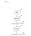
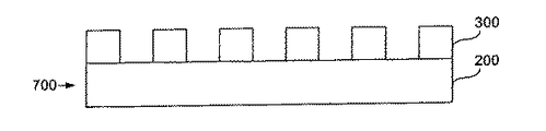
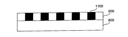
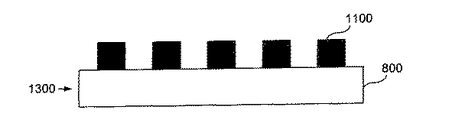
図1は、本発明の実施形態によるシステム100を示している。システム100は、照明光学系104に光を放出する照明源102を有している。照明光学系104は、光をマスク又はレチクル106を通過させ(又は反射させ)、投影光学系110を介して基板108に送る。このシステムの1つの実施形態はリソグラフィシステム、または同様のものであることができる。別の実施形態はホログラフィシステムであることができる。照明光学系104は、回折素子(図示されていないが、以下でさらに詳しく説明される素子700(図7)又は素子1300(図13)が例である)を有することができ、この回折素子は、照明エネルギを再分配するのを助けるために使用されることができる。
本発明の様々な実施形態は上に説明されているが、これらの実施形態は、限定ではなく例としてのみ示されていることが理解されるべきである。本発明の思想及び範囲から逸脱することなく実施形態において形式及び詳細の様々な変更を行うことができることは当業者にとって明らかとなるであろう。つまり、本発明の広さ及び範囲は、上記の典型的な実施形態の何れによっても限定されるべきではなく、請求項及び請求項の均等物に基づいてのみ定義されるべきである。
Claims (11)
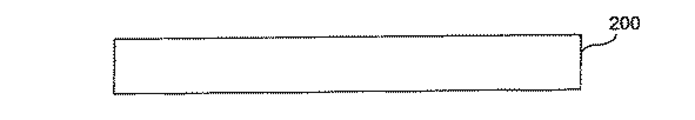
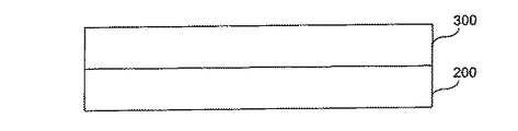
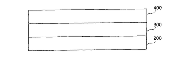
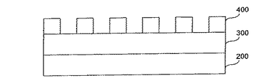
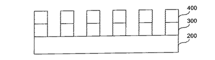
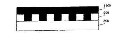
- 約100nm〜約300nmの波長を有する光を透過する回折素子を形成する方法であって、
約100nm〜約300nmの波長を有する前記光を当該光の実質的な減衰なしに透過する基板を提供し、
前記基板上に、約100nm〜約300nmの波長を有する前記光を当該光の実質的な減衰なしに透過することができる、約100nm〜約300nmの厚さを有するレジスト層を形成し、
前記レジスト層にパターンを露光し、
前記露光されたパターンに基づきレジスト層の一部をエッチングして除去し、
前記パターニングされたレジスト層上に非晶質等方性層を形成し、
前記パターニングされたレジスト層に基づき前記非晶質等方性層の一部を研磨して除去し、
前記レジスト層の残りの部分をエッチングして除去する、
ことを特徴とする方法。 - 前記回折格子が形成される前記基板として光学素子が提供される、請求項1記載の方法。
- 前記回折格子が形成される前記基板としてレンズが提供される、請求項1記載の方法。
- 前記回折格子が形成される前記基板としてミラーが提供される、請求項1記載の方法。
- 前記基板がフッ化バリウムから形成される、請求項1記載の方法。
- 前記基板がフッ化カルシウムから形成される、請求項1記載の方法。
- 前記非晶質等方性層が二酸化ケイ素から形成される、請求項1記載の方法。
- 前記非晶質等方性層の前記エッチングして除去するステップが、前記非晶質等方性層の一部のみを除去する材料を使用することを含む、請求項1記載の方法。
- 前記レジスト層の前記エッチングして除去するステップが、前記レジスト層の一部のみを除去する材料を使用することを含む、請求項1記載の方法。
- 前記基板が層の厚さを制御するためのストッパとして作用する、請求項1記載の方法。
- 前記基板が約1mm〜約6mmの厚さを有する、請求項1記載の方法。
Applications Claiming Priority (1)
| Application Number | Priority Date | Filing Date | Title |
|---|---|---|---|
| US10/625,704 US20050018296A1 (en) | 2003-07-24 | 2003-07-24 | Diffractive optical element and method of making same |
Publications (2)
| Publication Number | Publication Date |
|---|---|
| JP2005043900A JP2005043900A (ja) | 2005-02-17 |
| JP4199708B2 true JP4199708B2 (ja) | 2008-12-17 |
Family
ID=34080256
Family Applications (1)
| Application Number | Title | Priority Date | Filing Date |
|---|---|---|---|
| JP2004217818A Expired - Fee Related JP4199708B2 (ja) | 2003-07-24 | 2004-07-26 | 回折光学素子及び回折光学素子を形成する方法 |
Country Status (2)
| Country | Link |
|---|---|
| US (3) | US20050018296A1 (ja) |
| JP (1) | JP4199708B2 (ja) |
Families Citing this family (3)
| Publication number | Priority date | Publication date | Assignee | Title |
|---|---|---|---|---|
| US20050018296A1 (en) * | 2003-07-24 | 2005-01-27 | Asml Holding Nv | Diffractive optical element and method of making same |
| FR2968094B1 (fr) * | 2010-11-25 | 2012-12-07 | Centre Nat Rech Scient | Photobioreacteur solaire a dilution controlee du flux en volume |
| CN103818873B (zh) * | 2014-01-09 | 2016-08-31 | 合肥工业大学 | 一种大厚度、高深宽比的全金属沟道型微结构的加工方法 |
Family Cites Families (7)
| Publication number | Priority date | Publication date | Assignee | Title |
|---|---|---|---|---|
| US5985545A (en) * | 1996-03-19 | 1999-11-16 | Yamamoto; Nobuto | Diagnostic and prognostic ELISA assays of serum α-N-acetylgalactosaminidase for AIDS |
| US5982545A (en) * | 1997-10-17 | 1999-11-09 | Industrial Technology Research Institute | Structure and method for manufacturing surface relief diffractive optical elements |
| JPH11237503A (ja) * | 1997-12-03 | 1999-08-31 | Canon Inc | 回折光学素子及びそれを有する光学系 |
| WO2000020928A1 (en) * | 1998-10-08 | 2000-04-13 | Rochester Institute Of Technology | Photomask for projection lithography at or below about 160 nm and a method |
| JP4006226B2 (ja) * | 2001-11-26 | 2007-11-14 | キヤノン株式会社 | 光学素子の製造方法、光学素子、露光装置及びデバイス製造方法及びデバイス |
| US6852454B2 (en) * | 2002-06-18 | 2005-02-08 | Freescale Semiconductor, Inc. | Multi-tiered lithographic template and method of formation and use |
| US20050018296A1 (en) * | 2003-07-24 | 2005-01-27 | Asml Holding Nv | Diffractive optical element and method of making same |
-
2003
- 2003-07-24 US US10/625,704 patent/US20050018296A1/en not_active Abandoned
-
2004
- 2004-07-26 JP JP2004217818A patent/JP4199708B2/ja not_active Expired - Fee Related
-
2005
- 2005-01-25 US US11/041,409 patent/US20050157391A1/en not_active Abandoned
-
2007
- 2007-04-16 US US11/735,785 patent/US20070183046A1/en not_active Abandoned
Also Published As
| Publication number | Publication date |
|---|---|
| US20050018296A1 (en) | 2005-01-27 |
| US20050157391A1 (en) | 2005-07-21 |
| JP2005043900A (ja) | 2005-02-17 |
| US20070183046A1 (en) | 2007-08-09 |
Similar Documents
| Publication | Publication Date | Title |
|---|---|---|
| KR100890665B1 (ko) | 이중층 레티클 블랭크 및 이것의 제조방법 | |
| US7592107B2 (en) | Polarized reticle, photolithography system, and method of fabricating a polarized reticle | |
| JP2007128115A (ja) | 誘起されたトポグラフィおよび導波路効果を減少させるための位相シフト・マスクおよびプレーナ位相シフト・マスク用の埋め込み型エッチング停止部 | |
| TW200926263A (en) | Resolution enhancement techniques combining four beam interference-assisted lithography with other photolithography techniques | |
| EP1744211A1 (en) | Substrate, lithographic multiple exposure method, machine readable medium | |
| JPH06266095A (ja) | レティクル及びレティクル・ブランク | |
| JP2006156422A (ja) | パターン形成方法、電子デバイス製造方法、及び電子デバイス | |
| US11022874B2 (en) | Chromeless phase shift mask structure and process | |
| US6455203B1 (en) | Mask structure and method of manufacturing the same | |
| US8815475B2 (en) | Reticle carrier | |
| JP4199708B2 (ja) | 回折光学素子及び回折光学素子を形成する方法 | |
| US6015640A (en) | Mask fabrication process | |
| JP2000021716A (ja) | 露光装置及びこれを用いたデバイスの製造方法 | |
| US11036129B2 (en) | Photomask and method for forming the same | |
| JP3210705B2 (ja) | 位相シフトフォトマスク | |
| JP2009054739A (ja) | 光学素子及び露光装置 | |
| KR20090068898A (ko) | 위상 쉬프트 마스크의 제조 방법 | |
| WO2000039638A1 (en) | Method and apparatus for producing mask | |
| JPH09230576A (ja) | 投影露光方法 |
Legal Events
| Date | Code | Title | Description |
|---|---|---|---|
| RD04 | Notification of resignation of power of attorney |
Free format text: JAPANESE INTERMEDIATE CODE: A7424 Effective date: 20060914 |
|
| A521 | Request for written amendment filed |
Free format text: JAPANESE INTERMEDIATE CODE: A821 Effective date: 20060915 |
|
| RD03 | Notification of appointment of power of attorney |
Free format text: JAPANESE INTERMEDIATE CODE: A7423 Effective date: 20060904 |
|
| A977 | Report on retrieval |
Free format text: JAPANESE INTERMEDIATE CODE: A971007 Effective date: 20070829 |
|
| A131 | Notification of reasons for refusal |
Free format text: JAPANESE INTERMEDIATE CODE: A131 Effective date: 20070910 |
|
| A521 | Request for written amendment filed |
Free format text: JAPANESE INTERMEDIATE CODE: A523 Effective date: 20071210 |
|
| A02 | Decision of refusal |
Free format text: JAPANESE INTERMEDIATE CODE: A02 Effective date: 20080115 |
|
| A521 | Request for written amendment filed |
Free format text: JAPANESE INTERMEDIATE CODE: A523 Effective date: 20080410 |
|
| A911 | Transfer to examiner for re-examination before appeal (zenchi) |
Free format text: JAPANESE INTERMEDIATE CODE: A911 Effective date: 20080519 |
|
| A131 | Notification of reasons for refusal |
Free format text: JAPANESE INTERMEDIATE CODE: A131 Effective date: 20080725 |
|
| A521 | Request for written amendment filed |
Free format text: JAPANESE INTERMEDIATE CODE: A523 Effective date: 20080811 |
|
| TRDD | Decision of grant or rejection written | ||
| A01 | Written decision to grant a patent or to grant a registration (utility model) |
Free format text: JAPANESE INTERMEDIATE CODE: A01 Effective date: 20080904 |
|
| A01 | Written decision to grant a patent or to grant a registration (utility model) |
Free format text: JAPANESE INTERMEDIATE CODE: A01 |
|
| A61 | First payment of annual fees (during grant procedure) |
Free format text: JAPANESE INTERMEDIATE CODE: A61 Effective date: 20081003 |
|
| FPAY | Renewal fee payment (event date is renewal date of database) |
Free format text: PAYMENT UNTIL: 20111010 Year of fee payment: 3 |
|
| R150 | Certificate of patent or registration of utility model |
Free format text: JAPANESE INTERMEDIATE CODE: R150 |
|
| FPAY | Renewal fee payment (event date is renewal date of database) |
Free format text: PAYMENT UNTIL: 20111010 Year of fee payment: 3 |
|
| FPAY | Renewal fee payment (event date is renewal date of database) |
Free format text: PAYMENT UNTIL: 20121010 Year of fee payment: 4 |
|
| FPAY | Renewal fee payment (event date is renewal date of database) |
Free format text: PAYMENT UNTIL: 20121010 Year of fee payment: 4 |
|
| FPAY | Renewal fee payment (event date is renewal date of database) |
Free format text: PAYMENT UNTIL: 20131010 Year of fee payment: 5 |
|
| R250 | Receipt of annual fees |
Free format text: JAPANESE INTERMEDIATE CODE: R250 |
|
| R250 | Receipt of annual fees |
Free format text: JAPANESE INTERMEDIATE CODE: R250 |
|
| R250 | Receipt of annual fees |
Free format text: JAPANESE INTERMEDIATE CODE: R250 |
|
| R250 | Receipt of annual fees |
Free format text: JAPANESE INTERMEDIATE CODE: R250 |
|
| LAPS | Cancellation because of no payment of annual fees |