JP4183726B2 - Electronic neutralization device - Google Patents
Electronic neutralization device Download PDFInfo
- Publication number
- JP4183726B2 JP4183726B2 JP2006503600A JP2006503600A JP4183726B2 JP 4183726 B2 JP4183726 B2 JP 4183726B2 JP 2006503600 A JP2006503600 A JP 2006503600A JP 2006503600 A JP2006503600 A JP 2006503600A JP 4183726 B2 JP4183726 B2 JP 4183726B2
- Authority
- JP
- Japan
- Prior art keywords
- voltage
- target
- energy storage
- storage capacitor
- gap
- Prior art date
- Legal status (The legal status is an assumption and is not a legal conclusion. Google has not performed a legal analysis and makes no representation as to the accuracy of the status listed.)
- Expired - Fee Related
Links
Images


Classifications
-
- F—MECHANICAL ENGINEERING; LIGHTING; HEATING; WEAPONS; BLASTING
- F41—WEAPONS
- F41H—ARMOUR; ARMOURED TURRETS; ARMOURED OR ARMED VEHICLES; MEANS OF ATTACK OR DEFENCE, e.g. CAMOUFLAGE, IN GENERAL
- F41H13/00—Means of attack or defence not otherwise provided for
- F41H13/0012—Electrical discharge weapons, e.g. for stunning
-
- F—MECHANICAL ENGINEERING; LIGHTING; HEATING; WEAPONS; BLASTING
- F41—WEAPONS
- F41B—WEAPONS FOR PROJECTING MISSILES WITHOUT USE OF EXPLOSIVE OR COMBUSTIBLE PROPELLANT CHARGE; WEAPONS NOT OTHERWISE PROVIDED FOR
- F41B15/00—Weapons not otherwise provided for, e.g. nunchakus, throwing knives
-
- F—MECHANICAL ENGINEERING; LIGHTING; HEATING; WEAPONS; BLASTING
- F41—WEAPONS
- F41C—SMALLARMS, e.g. PISTOLS, RIFLES; ACCESSORIES THEREFOR
- F41C3/00—Pistols, e.g. revolvers
-
- H—ELECTRICITY
- H05—ELECTRIC TECHNIQUES NOT OTHERWISE PROVIDED FOR
- H05C—ELECTRIC CIRCUITS OR APPARATUS SPECIALLY DESIGNED FOR USE IN EQUIPMENT FOR KILLING, STUNNING, OR GUIDING LIVING BEINGS
- H05C1/00—Circuits or apparatus for generating electric shock effects
- H05C1/04—Circuits or apparatus for generating electric shock effects providing pulse voltages
Description
本発明は動物または人間の標的を無力化するための装置、および電極と標的との間のエアギャップを有する回路内で電極と標的を通過する電流を供給するための方法に関する。 The present invention relates to an apparatus for neutralizing an animal or human target, and to a method for supplying a current through the electrode and target in a circuit having an air gap between the electrode and the target.
最初のスタンガンは1960年代にJack Coverによって考案された。そのような先行技術のスタンガンは、標的を通って流れる電流が標的の神経筋肉系に妨害を与えるように一連の高電圧パルスを標的の皮膚に供給することによって標的を無力化する。低い電力システムは衝撃効果を生じさせる。高い電力システムは不随意筋収縮を生じさせる。スタンガンのような電子式無力化装置は2つの設計で作製されてきた。第1の設計は銃に固定された電極を有する。動作時に、使用者は標的に対する電極の直接接触を達成する。第2の設計は一対のダーツを発射することによって遠隔の標的に動作する。各々のダーツは電極を含み、それが通常では棘のある先端を有する。ダーツは標的の着ている衣服に係合するか、または標的の皮膚に係合するかのどちらかである。ほとんどのケースで、電極の一方もしくは両方が標的の皮膚を貫通せずに標的の衣服に接触するので、電極の一方もしくは両方と標的の皮膚との間に高インピーダンスのエアギャップが存在する。 The first stun gun was invented by Jack Cover in the 1960s. Such prior art stun guns neutralize the target by supplying a series of high voltage pulses to the target skin such that the current flowing through the target interferes with the target neuromuscular system. A low power system creates an impact effect. High power systems cause involuntary muscle contractions. Electronic neutralization devices such as stun guns have been made in two designs. The first design has electrodes fixed to the gun. In operation, the user achieves direct contact of the electrode with the target. The second design operates on a remote target by firing a pair of darts. Each dart includes an electrode, which usually has a barbed tip. The dart either engages the target wearing garment or engages the target skin. In most cases, there is a high impedance air gap between one or both of the electrodes and the target skin because one or both of the electrodes contact the target clothing without penetrating the target skin.
従来式のスタンガン100は図1の機能ブロック図に従って導入されることが可能である。スタンガン100では、安全スイッチS1を閉じる操作がバッテリー102をマイクロプロセッサ回路124へと接続し、スタンガン100を「武装状態」および発砲設定に準備の整った状態にセットする。それに続いてトリガスイッチS2を閉じる操作は、マイクロプロセッサ124が高電圧電源104を作動させる原因となる。高電圧電源104は約2,000ボルトのパルス電圧を出力し、それがコンデンサ106を2,000ボルト電源出力電圧へと充電するように連結される。スパークギャップGAP1の電圧が空気の電離電圧を超えるとき、変圧器108の一次巻き線に比較的高い電圧が現れる。変圧器108はこの電圧を、電極E1とE2にまたがる約50,000ボルトへと昇圧し、インピーダンスZ1を有する負荷としてモデル化された標的でエアギャップGAPAとGAPB内の空気を電離させる。それにより、比較的高い電圧が負荷Z1に印加される。コンデンサ106の出力電圧は急速に低下するのでスパークギャップGAP1を流れる電流が減少し、スパークギャップ内の空気を脱イオン化させ、開回路インピーダンスを復旧させる。スパークギャップGAP1のこの「再開放」は電極E1とE2に供給される各出力パルスの終局を規定する。図1に例示されたタイプの通常のスタンガンは毎秒5から20パルスを作り出す。
A
アリゾナ州ScottsdaleのTaser International社は数年間、図1に例示されたタイプでTaser(登録商標)Model M18およびModel M26スタンガンで指定されるスタンガンを製造してきた。これらのような高出力スタンガンは、通常、約0.2から約0.88マイクロファラッドのキャパシタンスを有するエネルギー貯蔵用コンデンサ106を組み入れる。
For several years, Taser International, Scottsdale, Arizona has manufactured stun guns designated by the Taser® Model M18 and Model M26 stun guns of the type illustrated in FIG. High power stun guns such as these typically incorporate an
皮製または布製のジャケットのような衣服を着ている可能性の高い標的を無力化することが望まれる。衣服は、標的の皮膚と電極との間に約0.6cm(0.25インチ)から約2.5cm(1インチ)のギャップを確立するように機能する。約50,000ボルトの出力電圧はこの長さのエアギャップを電離させ、標的内で筋肉収縮を誘発させるために充分な電流を支えるであろう。M18およびM26スタンガンのような高出力スタンガンで、離れたスタンガン出力電極間に流れる電流の大きさは数多くのグループの骨格筋を堅く収縮させることが可能である。人間の標的に関すると、スタンガンは標的に直立して平衡のとれた姿勢を維持する能力を喪失させる。結果として、標的は地面に倒れ、無力化される。 It is desirable to neutralize targets that are likely to be wearing clothes such as leather or fabric jackets. The garment functions to establish a gap of about 0.6 cm (0.25 inch) to about 2.5 cm (1 inch) between the target skin and the electrode. An output voltage of about 50,000 volts will ionize this length of air gap and support enough current to induce muscle contraction in the target. With high power stun guns such as the M18 and M26 stun guns, the magnitude of the current flowing between the distant stun gun output electrodes can tightly contract many groups of skeletal muscles. When it comes to human targets, stun guns lose their ability to stand upright and maintain a balanced posture. As a result, the target falls to the ground and is neutralized.
約50,000ボルトで、出力電極E1、E2と標的との間のGAPAとGAPBのうちの一方または両方にある空気が電離し、電極E1、E2を通って電流が流れ始める。電極E1、E2が高インピーダンスのエアギャップもしくはギャップではなく比較的低インピーダンスの負荷Z1を与えられるとき、スタンガンの出力電圧は大幅に低い電圧レベルへと降下するであろう。例えば、人間の標的およびプローブからプローブまで約25cm(10インチ)の分離距離を伴なうと、モデルM26スタンガンの出力電圧は約55,000ボルトから約5,000ボルトへと降下する可能性が高い。従来式のスタンガンは極めて高く無限大に近いインピーダンスのエアギャップの電気アークを堅実に作り出すための単一のモードだけで動作するように調整されているので、そのようなスタンガンはこの急速な電圧降下を示す。標的に電極およびエアギャップもしくはギャップを通過する低インピーダンス回路が形成されるとその後に、スタンガンの実効負荷インピーダンスは標的のインピーダンスである1,000オームまたはそれ未満に向かって減少する。通常の人間被験者は約200オームの負荷インピーダンスを提示する可能性が高い。 At about 50,000 volts, the air in one or both of GAP A and GAP B between the output electrodes E1, E2 and the target is ionized and current begins to flow through the electrodes E1, E2. When the electrodes E1, E2 are provided with a relatively low impedance load Z1 rather than a high impedance air gap or gap, the stun gun output voltage will drop to a significantly lower voltage level. For example, with a human target and a separation distance of about 25 cm (10 inches) from probe to probe, the output voltage of the model M26 stun gun is likely to drop from about 55,000 volts to about 5,000 volts. . Because conventional stun guns are tuned to operate in only a single mode to consistently produce an air gap electric arc with extremely high and near infinity impedance, such stun guns have this rapid voltage drop. Indicates. After the electrode and air gap or low impedance circuit passing through the gap is formed at the target, the stun gun's effective load impedance decreases towards the target impedance of 1,000 ohms or less. A normal human subject is likely to present a load impedance of about 200 ohms.
従来式のスタンガンは、標的で1つまたは複数の極めて高いインピーダンスのエアギャップの電離を引き起こす能力を有するようにやむを得ず設計されてきた。結果として、そのようなスタンガンは約50,000から約60,000ボルトの出力を作り出すように設計されてきた。電離の後にギャップのインピーダンスは極めて低いレベルへと下げられるが、それでもまだスタンガンは同じモードで動作し続け、今では極めて低いインピーダンスである標的に電流または電荷を供給する。その結果、上記で検討した従来式の高出力で高電圧のスタンガン100は比較的非効率的に動作し、相対的に高いバッテリー電力消費で相対的に低い電気−筋肉効果を生じる。
Conventional stun guns have been inevitably designed to have the ability to cause ionization of one or more very high impedance air gaps at the target. As a result, such stun guns have been designed to produce an output of about 50,000 to about 60,000 volts. After ionization, the gap impedance is lowered to a very low level, but the stun gun still continues to operate in the same mode, supplying current or charge to a target that is now very low impedance. As a result, the conventional high power, high
M26スタンガンはコンデンサ106で測定されるとき、約26ワットの出力電力を供給する。高電圧電源の非効率のせいで、バッテリーは毎秒15パルスのパルス繰り返し数で約35ワットを供給する。高電圧で高電力の出力信号を発生する必要条件のせいで、M26スタンガンは相対的に大型で相対的に重い8AAセルのバッテリーパック102を必要とする。付け加えると、M26スタンガンの電力発生用ソリッドステート部品104、コンデンサ106、昇圧用変圧器108、および変圧器108の一次側にある関連部品類はは比較的大電流かつ高電圧(2,000ボルト)で動作しなければならず、変圧器108の二次側の部品類はさらに高い電圧(50,000ボルト)への繰り返し暴露で動作しなければならない。
The M26 stun gun provides approximately 26 watts of output power as measured by
本発明の装置および方法を伴なわないと、電子式無力化装置を製造し、動作させるコストは法的処置および個人の安全のためのこれらの武器の広範な用途を制限するであろう。 Without the device and method of the present invention, the cost of manufacturing and operating an electronic neutralization device would limit the widespread use of these weapons for legal action and personal safety.
標的を無力化するための本発明の様々な態様による電子式無力化装置は標的上で第1および第2の離れた接触先端を確立するための第1および第2の電極と、標的上で第1および第2の接触先端間に供給される出力電圧を発生し、一方の電極で正の電位、他方の電極で負の電位を発生するための高電圧電源を有する。 An electronic disabling device according to various aspects of the present invention for disabling a target includes first and second electrodes for establishing first and second spaced contact tips on the target, and on the target. A high voltage power source is provided for generating an output voltage supplied between the first and second contact tips and generating a positive potential at one electrode and a negative potential at the other electrode.
本発明の様々な態様による標的の無力化のための方法は、標的でエアギャップを電離させるために第1の貯蔵エネルギー装置から標的へと第1の信号を供給する工程、およびギャップを通過し、標的を通過する電流を持続するために第2の貯蔵エネルギー装置から標的へと第2の信号を供給する工程を含む。 A method for disabling a target according to various aspects of the present invention includes providing a first signal from a first stored energy device to a target to ionize an air gap at the target, and passing through the gap. Supplying a second signal from the second stored energy device to the target to sustain the current passing through the target.
本発明の様々な態様による標的の無力化のための装置は、標的でエアギャップを電離させるために第1の貯蔵エネルギー装置から標的へと第1の信号を供給するための回路、およびギャップを通過し、標的を通過する電流を持続するために第2の貯蔵エネルギー装置から標的へと第2の信号を供給するための回路を有する。 An apparatus for target neutralization according to various aspects of the present invention includes a circuit for supplying a first signal from a first stored energy device to a target to ionize an air gap at the target, and a gap. A circuit is provided for supplying a second signal from the second stored energy device to the target for passing and sustaining current passing through the target.
バッテリーによって動作させられる装置のためにバッテリーの容量をモニタするための本発明の様々な態様による方法は、装置の複数のモードのうちの動作しているモードをモニタする工程、本来のバッテリー容量の目印と、複数のうちの各動作モードに付随するバッテリー容量消費の率の目印を保存する工程、および消費されるバッテリー容量を、動作モードモニタ手段、動作時間モニタ手段、およびメモリから受け取るデータに基づいて計算する工程を含む。 A method according to various aspects of the present invention for monitoring battery capacity for a battery operated device comprises the steps of monitoring an operating mode of a plurality of modes of the device; A step of storing a mark and a mark of the rate of battery capacity consumption associated with each of the plurality of operation modes, and the consumed battery capacity based on data received from the operation mode monitoring means, the operation time monitoring means, and the memory; And calculating.
装置のための、本発明の様々な態様による保証情報システムは、保証の持続時間の目印を保存するための回路、保証に関して開始時間を保存するための回路、および装置を動作させるために電力を供給するための回路を有する。本システムはさらに、オペレータが取り替え可能な装置の部品として供給されることが可能であり、取り替えシステムは延長された保証を容易にする。 A warranty information system according to various aspects of the present invention for a device includes a circuit for storing a mark of duration of warranty, a circuit for storing a start time with respect to the warranty, and power to operate the device. A circuit for supplying; The system can further be supplied as part of an operator replaceable device that facilitates extended warranty.
保証によって守られる装置のプロセッサへと保証情報を提供するための本発明の様々な態様による方法は、保証の持続時間の目印を保存する工程、保証に関して開始時間を保存する工程、および装置を動作させるために電力を供給する工程を含む。本方法はさらに、オペレータが取り替え可能な装置の部品として取り替えモジュールを供給する工程を含むことが可能であり、それが目印の保存、開始時間の保存、電力の供給、それによる延長保証の容易化を実行する。 A method according to various aspects of the present invention for providing warranty information to a processor of a device protected by a warranty includes storing a warranty duration landmark, storing a start time with respect to the warranty, and operating the device. Supplying power to generate power. The method may further include providing a replacement module as part of the replaceable device by the operator, which saves the landmark, saves the start time, supplies power, thereby facilitating extended warranty. Execute.
本発明のシステムおよび方法が図面を参照しながら説明されるであろうが、ここでは類似した番号は類似した素子を示す。 The system and method of the present invention will be described with reference to the drawings, wherein like numerals indicate like elements.
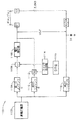
本発明の様々な態様による電子式無力化装置は動物または人(例えば標的)を一時的に無力化し、装置からの電流が標的を通り抜けている間はある程度標的を動けなくしおよびび/または無力化することが可能である。例えば、図2の電子式無力化装置200は電源202、第1および第2のエネルギー貯蔵用コンデンサ204および210、および各々がSPSTスイッチとして動作し、かつ2つのエネルギー貯蔵用コンデンサを下流の回路素子へと選択的に接続することに役立つスイッチS1およびS2を有する。本明細書で検討されるようなコンデンサを導入するためにいずれかの数の並列もしくは直列接続の物理的コンデンサが使用されることが可能である。スイッチは、スパークギャップおよび/または電子スイッチ(例えばトランジスタ)といったいずれかの従来式の方式で導入されることが可能である。コンデンサ204はスイッチS1によって選択的に電圧増倍器208へと接続され、電圧増倍器208が第1および第2の電極E1およびE2へと連結される。電極は固定されることが可能であり、あるいは上記で検討したようにダーツの中に導入されることが可能である。コンデンサ204および210もやはり共通の導体(回路接地)を通して電極E2へと連結される。
An electronic disabling device according to various aspects of the present invention temporarily disables an animal or a person (eg, a target), and to some extent the target is immobile and / or neutralized while the current from the device is passing through the target. Is possible. For example, the electronic disabling
トリガ216(例えば銃の引き金に類似したスイッチ)は、スイッチS1 206およびS2 212のタイミングおよび閉操作を制御するスイッチ制御器214を制御する。
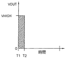
装置200の動作によって供給され、電極E1とE2間の出力電圧VOUTは2つの回路部分201および203の各々によって供給される電圧の重ね合わせである。動作では、時間T0に電源202が作動させられる。時間間隔T0〜T1の間にコンデンサ204および210が充電される。図3の時間T1に、スイッチ制御器214がスイッチS1を閉じることでコンデンサ204を電圧増倍器208へと連結する。図3はVOUTを期間T1からT2までの間の相対的に高い電圧として示している。
A trigger 216 (eg, a switch similar to a gun trigger) controls a
Supplyed by the operation of the
図5に例示された仮定の状況では、電極E1と標的の接触点E3との間に高インピーダンスのエアギャップが存在し、電極E2と標的の接触点E4との間に皮膚接触が存在する。皮膚接触は低い(例えばゼロに近い)インピーダンスを与える。接触点E3およびE4は上記で検討したように標的上で間隔を置かれている。抵抗器とZLOADの記号は標的内部の抵抗を表し、通常では1,000オーム未満であり、通常の人間の標的では約200オームである可能性が高い。 In the hypothetical situation illustrated in FIG. 5, there is a high impedance air gap between the electrode E1 and the target contact point E3, and there is skin contact between the electrode E2 and the target contact point E4. Skin contact provides a low (eg, near zero) impedance. Contact points E3 and E4 are spaced on the target as discussed above. The resistor and Z LOAD symbols represent the internal resistance of the target, typically less than 1,000 ohms, and likely to be about 200 ohms for a normal human target.
E1からE3に渡ってギャップGAPAにVHIGH電圧を印加する操作はギャップ内の空気を電離させてアークを形成する。その結果、GAPAのインピーダンスは図7のように無限大近い量からゼロに近い量へと降下し、図6のような回路構成を作り出す。E1からE3へのこの低インピーダンスの電離した経路がVHIGH出力信号の短い持続時間の印加によって確立された後、図4の期間T2からT3への間にスイッチ制御器214がスイッチS1を開き、スイッチS2を閉じることで例示されるようにコンデンサ210を電極E1およびE2へと連結する。コンデンサ210は電離を持続させ、有意の追加的時間間隔に関してGAPAのアークを維持する。これが続くと、間隔T2からT3の間のコンデンサ210の低電圧の放電が標的を通過させて多量の電荷を移動させることで標的を無力化する。標的を通過するコンデンサ210の継続した放電はコンデンサ210に貯蔵された電荷を結局は使い果たし、最終的に出力電圧をGAPA内で電離がもはや支えられない電圧へと降下させるであろう。その後、GAPAは非イオン化状態の高インピーダンス状態に戻り、標的を通過して流れる電流を停止させるであろう。図8および9は時間T0〜T3に関して電極間の電圧を例示している。
The operation of applying the V HIGH voltage to the gap GAP A from E1 to E3 ionizes the air in the gap to form an arc. As a result, the impedance of GAP A drops from an amount close to infinity as shown in FIG. 7 to an amount close to zero, creating a circuit configuration as shown in FIG. After this low impedance ionized path from E1 to E3 is established by applying a short duration of the V HIGH output signal, the
スイッチ制御器214は予め決められた時間的期間についてスイッチS1を閉じ、その後、予め決められた時間的期間についてスイッチS2を閉じるようにプログラムされることが可能である。
The
間隔T3からT4の間では、工場で設定したパルス繰り返し数を維持するために電源202は無効にされる。図9および10のタイミング図に例示されるように、この工場設定のパルス繰り返し数はT0からT4の時間的間隔全体、および時間T0からT4にそれぞれ対応する時間T4からT8のようなその繰り返しを規定する。マイクロプロセッサによって実行されるタイミング制御回路はT3からT4の時間的期間の間でスイッチS1およびS2を開状態に維持し、所望のT0からT4の時間的期間が完了するときまで電源を無効にする。時間T4で、コンデンサ204および210を電源出力電圧に再充電するために電源が再び作動させられるであろう。
In the interval T3 to T4, the
別の代替選択肢の実施例では、間隔T2からT3への持続時間が延長されることが可能である。例えば、図11の電子式無力化装置1100は上述の部品類を有し、さらに第3のコンデンサ1118およびダイオードD1を有する。高電圧電源1102が並列のコンデンサ1110および1118を充電する。コンデンサ1102の第2の端子が接地電位に接続される一方で、コンデンサ1118の第2の端子はダイオードD1を通して接地電位へと戻される。
In another alternative embodiment, the duration from interval T2 to T3 can be extended. For example, the
図12の他の電子式無力化装置1200は、図11の機能ブロック図を参照して上記で検討された装置1100の機能の実施例である。装置1200では、高電圧電源1202は等しい出力電圧性能の2つの出力を供給する。各々の出力は、コンデンサ1204と1218(機能で上述の第1と第3のコンデンサに相当する)に電流I1を、コンデンサ1210(機能で上述の第2のコンデンサに相当する)に電流I2を供給する。高電圧電源1202の第1の電圧出力はまた、2,000ボルトのスパークギャップであるGAP1、および一次対二次巻き線の昇圧比1から25を有する出力変圧器1208の一次巻き線へも接続される。コンデンサ1210の第2の端子は接地電位へと接続され、その一方でコンデンサ1218の第2の端子は抵抗器R1を通して接地電位へと戻される。高電圧電源1202の第2の電圧出力もやはり3,000ボルトのスパークギャップであるGAP2へと接続される。
The other
スパークギャップGAP1およびGAP2は1から25の昇圧比を有する変圧器1208の一次巻き線および二次巻き線にそれぞれ直列である。
装置1200では、安全スイッチS1を閉じる操作が高電圧電源1202の動作を有効化し、機器構成を動作させるための待ち受け/準備完了状態に装置1200を設定する。トリガスイッチS2を閉じる操作は、マイクロプロセッサ1224が高電圧電源1202に作動信号を行使する状態を生じさせる。それに応答して、電源1202はコンデンサ1204と1218を充電する電流I1およびコンデンサ1210を充電する電流I2を流し始める。このコンデンサ充電時間間隔がここで、図13から18の電圧vs.時間のグラフを参照しながらさらに述べられるであろう。
Spark gaps GAP1 and GAP2 are in series with the primary and secondary windings of transformer 1208 having a step-up ratio of 1 to 25, respectively.
In the
T0からT1の間隔の中で、高電圧電源1202からの出力に応答してコンデンサ1204(C1)、1210(C2)、および1218(C3)は電圧ゼロから約2,000ボルトへと充電される。スパークギャップGAP1およびGAP2は無限大に近いインピーダンスで開いた状態を保っている。時間T1に、コンデンサC1およびC3の電圧はGAP1の破壊定格である2,000ボルトに近くなる。スパークギャップGAP1の破壊電圧で、GAP1にアークが形成され、GAP1のインピーダンスはゼロに近い量へと降下するであろう。この降下は図13〜16の時間T1に始まる。時間T1の開始時に、コンデンサC1が変圧器1208の一次巻き線を通じて放電を開始するであろう。変圧器1208の動作によって電極E1とE2間の電圧は図16に示されるように−50,000ボルトへと急速に低下する。コンデンサC1の電圧(図15)は約2,000ボルトから相対的に緩やかに低下し、その一方でスパークギャップGAP2の電圧はGAP2の破壊電圧に向かって相対的に緩やかに上昇する(図16)。
Capacitors 1204 (C1), 1210 (C2), and 1218 (C3) are charged from zero voltage to about 2,000 volts in response to the output from high
装置1200は出力電極E1とE2間の出力信号VOUTを供給する2つのモードを示す。第1の動作モードでは、GAPA内の空気を電離させるためにT1からT2の時間的間隔の間にコンデンサC1によって供給されるエネルギーを伴なって相対的に高い電圧が供給される。第2の動作モードでは、T2からT3の時間的間隔の間にコンデンサC2およびC3によって供給されるエネルギーを伴なって相対的に低い電圧が供給される。T1からT2への間隔の終わりに、スパークギャップGAP2とGAPAが低い(ゼロに近い)インピーダンスで導通するので、装置1200は動作の第2のモードでの動作を開始する。スパークギャップGAP2とGAPA内の空気は時間T2に電離させられ、電極E1とE2、および相対的に低いインピーダンスの標的の負荷を通してコンデンサC2とC3が放電することを可能にする。図17に例示されるように、コンデンサC1は時間がT2に近づくにつれてゼロに近い量へと放電している。スパークギャップGAP2が開いているのでコンデンサC1がT2の前に放電することはない。T2からT3への時間的間隔の間に、コンデンサC2とC3間の電圧はゼロへと低下するが、なぜならばこれらのコンデンサは出力端子E1とE2間に見られる低いインピーダンス(標的のみ)の負荷を通じて放電するからである。
図18はT2からT3への時間間隔中にGAP2の電圧、および電極E1およびE2間の電圧を提示している。T2からT3への間隔の間のうちの大部分で、電極E1およびE2間の電圧は約2,000ボルトよりも小さい絶対値を有する。 FIG. 18 presents the voltage of GAP2 and the voltage between electrodes E1 and E2 during the time interval from T2 to T3. During most of the interval from T2 to T3, the voltage between electrodes E1 and E2 has an absolute value less than about 2,000 volts.
本発明の様々な態様による電子式無力化装置では、コンデンサC1は約0.14マイクロファラッドを供給し、T1からT2への時間間隔約1.5マイクロ秒の間に放電することが可能である。コンデンサC2およびC3はそれぞれ約0.02マイクロファラッドを供給し、T2からT3への時間間隔約50マイクロ秒の間に放電することが可能である。 In an electronic disabling device according to various aspects of the present invention, capacitor C1 provides approximately 0.14 microfarads and can be discharged during a time interval from T1 to T2 of approximately 1.5 microseconds. Capacitors C2 and C3 each supply about 0.02 microfarads and can be discharged during a time interval of about 50 microseconds from T2 to T3.
他の実施例では、T1からT2への間隔の持続時間について他の持続時間が使用される。この持続時間は約1.5から約0.5マイクロ秒の範囲にあることが可能である。
他の実施例では、T2からT3への間隔の持続時間について他の持続時間が使用される。この持続時間は約20から約200マイクロ秒の範囲にあることが可能である。
In other embodiments, other durations are used for the duration of the interval from T1 to T2. This duration can be in the range of about 1.5 to about 0.5 microseconds.
In other embodiments, other durations are used for the duration of the interval from T2 to T3. This duration can be in the range of about 20 to about 200 microseconds.
T0からT1への間隔の持続時間は、装置1200を動作させるために充分な電流を供給しながらその一方でコンデンサC1、C2、およびC3を充電する電源1201の能力に応じて決まる。例えば、一部放電したバッテリーによる回路動作と比較すると、新品のバッテリー1201はT0からT1への時間間隔を短縮することが可能である。低温の周囲環境温度での装置1200の動作はバッテリー容量を低下させる可能性が高く、T0からT1への間隔を増加させる可能性もやはり高い。
The duration of the interval from T0 to T1 depends on the
図9および10を参照しながら検討したように予め決められたパルス繰り返し数で、上記で検討したように電子式無力化装置を操作することは大いに望ましい。1つの実施例では、制御器1214は本発明の様々な態様による方法を実行するようにプログラムされた従来式のマイクロプロセッサ回路を有する。本発明の様々な態様によると、制御器1214はデジタルパルス制御間隔の持続時間(図10)を制御し、その結果、サイクルの持続時間(図10のTAおよびTB)を制御するためにフィードバック信号に従って作動信号を高電圧電源1202に供給する。デジタルパルス制御間隔は上記で検討したT3からT4への間隔に相当する。
It is highly desirable to operate the electronic neutralizer as discussed above with a predetermined number of pulse repetitions as discussed with reference to FIGS. In one embodiment, the controller 1214 comprises a conventional microprocessor circuit programmed to perform the methods according to various aspects of the present invention. In accordance with various aspects of the present invention, controller 1214 controls the duration of the digital pulse control interval (FIG. 10) and, as a result, a feedback signal to control the duration of the cycle (TA and TB in FIG. 10). The operation signal is supplied to the high
例えば、図12の制御器1214はマイクロプロセッサ1224、およびフィードバック信号調整回路1222を有する。マイクロプロセッサ1224は高電圧電源1202からフィードバック信号調整回路1222を経由してフィードバック信号を受け取る。フィードバック信号調整回路はフィードバック信号に応答して状態信号をマイクロプロセッサ1224に供給する。マイクロプロセッサ1224は図4、7、8、9、10、17、および18に例示されるように時間T3に到達したときを検出する。動作サイクルの開始時間T0は知られているので、時間T3から予め設定されたパルス繰り返し数が実行されるために充分な時間(例えばT3からT4)までマイクロプロセッサは高電圧電源を遮断状態または無効化された動作モードに維持するであろう。T3からT4への間隔の持続時間は他の間隔を補償するために変わることが可能であるが、マイクロプロセッサは予め設定されたパルス繰り返し数を達成するようにT0からT4への時間間隔を維持する。
For example, the controller 1214 of FIG. 12 includes a
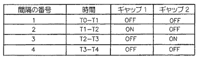
「Gap On/Off Timing」という表題の図19の表は4つの関連する動作時間間隔の中でのGAP1およびGAP2の構造の単純化された要約を表している。「off」構造は高インピーダンスの非電離のスパークギャップの状態を表し、「on」構造は電離した状態を表し、スパークギャップ破壊電圧が達成されている。 The table in FIG. 19 entitled “Gap On / Off Timing” represents a simplified summary of the structures of GAP1 and GAP2 during four related operating time intervals. The “off” structure represents a high impedance, non-ionized spark gap state, and the “on” structure represents an ionized state, and a spark gap breakdown voltage is achieved.
変更例の装置の行例では、従来式の絶縁材料を使用する小型の電子式無力化装置の設計を容易にするために装置内の電圧が下げられる。例えば、ある実施例は各々が出力電圧の半分を供給する二重の出力を有する電圧増倍器を使用することが可能である。その後、電極E1およびE2間の電圧が二重出力電圧の合計にされることが可能である。例えば、図20の電圧増倍回路2000は1つの一次巻き線、およびセンタータップ引き出し型または2つの分離型の二次巻き線を有する変圧器2008を有する。一次巻き線から二次巻き線への昇圧比は1対12.5である。それでも変圧器2008は約2,000ボルトの電源から約50,000ボルトの出力信号を発生させるために25対1の昇圧比を達成するという目標を成し遂げる。この二重二次型変圧器構造の1つの利点は、各々の二次巻き線に加えられる最大電圧が1つの二次巻き線を使用する設計と比べて50%削減されることである。そのような削減された二次巻き線動作電位は所定量の変圧器の絶縁でさらに高い出力電圧を達成するため、または出力変圧器の素子にさらに小さい高電圧ストレスを設定するために要求される可能性が高い。
In the modified device line example, the voltage in the device is lowered to facilitate the design of a small electronic neutralization device using conventional insulating materials. For example, one embodiment can use voltage multipliers with dual outputs, each providing half of the output voltage. Thereafter, the voltage between electrodes E1 and E2 can be summed to the double output voltage. For example, the voltage multiplication circuit 2000 of FIG. 20 includes a
上記で検討したようなTaser M26スタンガンによって代表される従来式のスタンガンと比較して、本発明の様々な態様による電子式無力化装置を使用することによって大幅で目覚しい恩典が達成されることが可能である。例えば、M26スタンガンは約0.88マイクロファラッドの単一のエネルギー貯蔵用コンデンサを利用する。2,000ボルトに充電されたとき、そのコンデンサは約1.76ジュールのエネルギーを貯蔵し、その後、各々の出力パルスの中で放電する。毎秒15パルスの標準的なパルス繰り返し数および1パルス当たり1.76ジュールに関すると、M26スタンガンは約35ワットの入力電力を必要とし、それは前に説明されたように、8連接続のAAアルカリ電池セルを利用する大型で比較的重いバッテリー電源によって供給されなければならない。 Compared to conventional stun guns represented by the Taser M26 stun gun as discussed above, significant and significant benefits can be achieved by using an electronic neutralization device according to various aspects of the present invention. It is. For example, the M26 stun gun utilizes a single energy storage capacitor of about 0.88 microfarad. When charged to 2,000 volts, the capacitor stores about 1.76 joules of energy and then discharges during each output pulse. With a standard pulse repetition rate of 15 pulses per second and 1.76 joules per pulse, the M26 stun gun requires about 35 watts of input power, which, as explained earlier, is an 8-wire AA alkaline battery. Must be supplied by a large, relatively heavy battery power source that utilizes the cell.
本発明の様々な態様による電子式無力化装置は次のようなキャパシタンス、すなわちC1で約0.07マイクロファラッドおよびC2で約0.01マイクロファラッドを有するコンデンサを使用することが可能である。C1とC2のキャパシタンスの合計は約0.08マイクロファラッドである。C1とC2に関してこれらの値を使用する電子式無力化装置200はこれらのコンデンサに貯蔵されるエネルギー約0.16ジュールから各々の出力パルスを供給する。毎秒約15パルスのパルス繰り返し数で、これら2つのコンデンサは約2.4ワットのバッテリー電力をコンデンサで消費し、バッテリーではおよそ3.5から4ワットである。結果として、バッテリーは単一のAAサイズのバッテリーであることが可能である。この電子式無力化装置は上記で検討されたM26スタンガンと比較して電力消費で90%の削減を達成する。
Electronic neutralization devices according to various aspects of the present invention can use capacitors having the following capacitances: about 0.07 microfarads at C1 and about 0.01 microfarads at C2. The total capacitance of C1 and C2 is about 0.08 microfarad. An
本発明の様々な態様による電子式無力化装置は図3および4に例示されるように時系列的に並べられ、整形された出力波形を発生する。この出力波形は2つの異なる負荷構造に対応し、T1からT2への第1の動作間隔の高インピーダンスの間の相対的に高い電圧出力の動作モード、およびT2からT3への第2の動作間隔の低インピーダンスの間の相対的に低い電圧出力の動作モードを与えられる。 Electronic neutralization devices according to various aspects of the present invention generate output waveforms that are arranged in time series and shaped as illustrated in FIGS. This output waveform corresponds to two different load structures, a relatively high voltage output operating mode between the high impedance of the first operating interval from T1 to T2, and a second operating interval from T2 to T3. The mode of operation of a relatively low voltage output is provided between the low impedances.
追加的な恩典として、回路素子は一層低い電力レベルおよび一層低い電圧レベルで動作し、その結果、さらに信頼性のある回路動作につながる。さらに、そのような電子式無力化装置は物理的にはるかに小型の設計で梱包されることが可能である。本発明の様々な態様によるスタンガンの実験用プロトタイプの実施形態では、M26スタンガンのサイズと比べてプロトタイプのサイズは約50%小さくされ、重量は約60%削減される。 As an additional benefit, circuit elements operate at lower power levels and lower voltage levels, resulting in more reliable circuit operation. Furthermore, such electronic neutralization devices can be physically packaged in a much smaller design. In an embodiment of a stun gun experimental prototype according to various aspects of the present invention, the prototype size is reduced by about 50% and the weight is reduced by about 60% compared to the size of the M26 stun gun.
本発明の他の態様によると、バッテリー容量が制御器によって推測される。さらに、バッテリー容量の読み出し値がユーザへと提供されることが可能である。ほとんどの電子装置では、残りのバッテリー容量は動作中のバッテリー電圧を測定するか、またはバッテリーの放電電流を経時的に積算するかのどちらかによって推測されることが可能である。上記で検討したいくつかの動作モードに起因して、先行技術のバッテリー管理は信頼性のない結果を生じる。周囲環境温度がバッテリー容量に強く影響を及ぼし、かつ電子式無力化装置が広範な周囲環境温度で必要とされるので、温度補償されていない先行技術のバッテリー容量推測方法はさらに信頼性のない結果を生じる。 According to another aspect of the invention, the battery capacity is estimated by the controller. In addition, a battery capacity reading can be provided to the user. In most electronic devices, the remaining battery capacity can be estimated either by measuring the operating battery voltage or by integrating the battery discharge current over time. Due to the several modes of operation discussed above, prior art battery management yields unreliable results. Prior art battery capacity estimation methods that are not temperature compensated are more unreliable because ambient temperature strongly affects battery capacity and electronic neutralization is required over a wide range of ambient temperatures Produce.
本発明の様々な態様による電子式無力化装置(例えば図12、21〜24)のバッテリー電力消費(例えば、図25)は次のように動作モードで変わる。1つの実施例では、本装置は上記で検討した素子に加えてリアルタイムクロック、レーザ、および投光器具を有する。リアルタイムクロックは約3.5マイクロアンペアの電流を消費する可能性が高い。システムの安全スイッチS1が武装状態にされれば、ここで作動するマイクロプロセッサとそのクロックは約4ミリアンペアの電流を消費する可能性が高い。有効化され、かつ安全スイッチが武装状態にされれば、レーザ目標照射器は約11ミリアンペアの電流を消費する可能性がある。有効化され、かつ安全スイッチが武装状態にされれば、前方を向いた低強度の2連白色LED投光器具は約63ミリアンペアの電流を消費する可能性が高い。安全スイッチが武装状態にされ、かつ引き金スイッチS2が引かれると、本装置は約3から約4アンペア電流引き出しするであろう。したがって、最小から最大の電流消費は約1,000,000対1の比で変わるであろう。 Battery power consumption (eg, FIG. 25) of an electronic disabling device (eg, FIG. 12, 21-24) according to various aspects of the present invention varies in operating mode as follows. In one embodiment, the apparatus has a real time clock, laser, and floodlight in addition to the elements discussed above. Real-time clocks are likely to consume about 3.5 microamperes of current. If the system safety switch S1 is armed, the microprocessor operating here and its clock are likely to consume about 4 milliamps of current. If enabled and the safety switch is armed, the laser target illuminator can consume about 11 milliamperes of current. If enabled and the safety switch is armed, a low-strength, double white LED floodlight facing forward is likely to consume about 63 milliamps of current. If the safety switch is armed and trigger switch S2 is pulled, the device will draw about 3 to about 4 amps of current. Thus, the minimum to maximum current consumption will vary at a ratio of about 1,000,000 to 1.
さらに事態を複雑にするが、システムのバッテリーモジュール内に詰められたリチウム電池の容量は動作温度範囲全体にわたって大幅に変化し得る。−20℃で、このバッテリーモジュールは約100回の5秒放電サイクルを供給することが可能である。+30℃では、このバッテリーモジュールは約350回の5秒放電サイクルを供給することが可能である。 To further complicate matters, the capacity of lithium batteries packed in the battery module of the system can vary significantly over the entire operating temperature range. At −20 ° C., this battery module can supply about 100 5-second discharge cycles. At + 30 ° C., the battery module can supply approximately 350 5 second discharge cycles.
最も温暖から最も寒冷の動作温度範囲、および最小から最大のバッテリー電流消費機能で、バッテリーの寿命は約5,000,000から1で変化する。
本発明の様々な態様によるバッテリー容量査定システムは、様々な負荷の下でかつ様々な温度条件下での臨界バッテリーパラメータの実験室測定に基づいて残りのバッテリー容量を推測する。これらの測定されたバッテリー容量パラメータは各々のバッテリーモジュールと共に含まれる電子式不揮発性メモリ装置内に一覧表として電子式に保存される(図22)。図21および22に例示されるように、適切なデータインターフェースの接触はマイクロプロセッサがバッテリーモジュール2200内に電子式に保存された一覧表と通信することを可能にし、それにより、バッテリー(2202および2204)の残りの容量を推測する。内蔵型電子式不揮発性メモリを備えたバッテリーモジュール2200はDigital Power Magazine(DPM)または単純にシステム・バッテリーモジュールと称されることが可能である。
Battery life varies from about 5,000,000 to 1 with the warmest to coldest operating temperature range and the minimum to maximum battery current consumption capability.
A battery capacity assessment system according to various aspects of the present invention estimates the remaining battery capacity based on laboratory measurements of critical battery parameters under various loads and under various temperature conditions. These measured battery capacity parameters are stored electronically as a list in an electronic nonvolatile memory device included with each battery module (FIG. 22). As illustrated in FIGS. 21 and 22, the appropriate data interface contacts allow the microprocessor to communicate with a list stored electronically in the battery module 2200, thereby providing the batteries (2202 and 2204). ) Guess the remaining capacity. The battery module 2200 with built-in electronic non-volatile memory can be referred to as a Digital Power Magazine (DPM) or simply a system battery module.
バッテリーモジュールに関してデータ表を作成するために必要とされるデータは、各々の温度区間でバッテリー性能と寿命を記録しながらその一方で、選択された温度で電子式無力化装置を動作させることによって収集された。 Data required to create a data table for the battery module is collected by operating the electronic neutralizer at a selected temperature while recording battery performance and life at each temperature interval It was done.
結果として得られたバッテリー容量測定値が集められ、図25に例示されるタイプの集計表へと体系化された。各システム特徴に関するバッテリー放電量のパラメータが計算され、その特徴の実用に合った動作条件に基づいてマイクロアンペア・アワー(μAH)で標準の放電量値へと変換された。例えば、クロックを活動させ続けるために必要とされるバッテリー放電量は、クロックを約24時間活動させ続けるために必要とされる電流を合計してμAHの数字で表される。マイクロプロセッサ、前向き投光器具、およびレーザ目標照射器に1秒間電源を入れるためのバッテリー放電量は別々の表記入事項によってμAHの値で表される。発砲モードで銃を動作させるために必要とされるバッテリー放電量は単一の電力出力パルスを発射するために必要なバッテリー放電量のμAHの数字によって表される。 The resulting battery capacity measurements were collected and organized into a summary table of the type illustrated in FIG. The battery discharge parameters for each system feature were calculated and converted to standard discharge values at microampere hours (μAH) based on operating conditions suitable for the feature's practical use. For example, the amount of battery discharge required to keep the clock active is represented by the number of μAH, summing the current required to keep the clock active for about 24 hours. The amount of battery discharge to power on the microprocessor, the forward light projector, and the laser target illuminator for 1 second is expressed in μAH values by separate table entries. The amount of battery discharge required to operate the gun in fire mode is represented by the number of μAH of battery discharge required to fire a single power output pulse.
要求されるすべての温度での動作を可能にするために、バッテリー放電および残りのバッテリー容量の追跡をし続けながら各々の温度増分で合計の利用可能なバッテリー容量が測定された。正規化された100%のバッテリー容量値を表すために25℃(周囲環境)でのμAHによるバッテリー容量が表の中にプログラムされた。25℃での総計(100%)のバッテリー容量の数字と調和するように他の温度でのバッテリー表放電量の数字が調節された。例えば、−20℃での合計のバッテリー容量は25℃でのバッテリー容量の約35%と測定されたので−20℃でのμAHの数字は1/0.35で増倍された。 In order to allow operation at all required temperatures, the total available battery capacity was measured at each temperature increment while continuing to track battery discharge and remaining battery capacity. The battery capacity in μAH at 25 ° C. (ambient environment) was programmed into the table to represent a normalized 100% battery capacity value. Battery surface discharge numbers at other temperatures were adjusted to match the total (100%) battery capacity numbers at 25 ° C. For example, the total battery capacity at −20 ° C. was measured to be about 35% of the battery capacity at 25 ° C., so the μAH figure at −20 ° C. was multiplied by 1 / 0.35.
使用されたバッテリー容量の追跡を続けるために上記で検討された表のためのメモリ内の追加的な場所(図25に示されていない)がマイクロプロセッサによって使用される。安全選択器が「武装状態」の位置に留まっている場合、この数字(すなわち使用されたバッテリー容量)は約1秒毎に更新され、安全選択器が「安全状態」の位置に留まっている場合、約24時間毎に更新される。残りのバッテリー容量のパーセンテージはこの数字を合計バッテリー容量で除算することによって算出される。本装置は残りのバッテリー容量のこのパーセントを、装置が武装状態にされる度に2桁のCentral Information Display(CID)に2秒間表示する。 An additional location in memory for the table discussed above (not shown in FIG. 25) is used by the microprocessor to keep track of the used battery capacity. If the safety selector stays in the “armed” position, this number (ie the used battery capacity) is updated approximately every second, and the safety selector stays in the “safe” position. , Updated about every 24 hours. The remaining battery capacity percentage is calculated by dividing this number by the total battery capacity. The device displays this percentage of remaining battery capacity on a two-digit central information display (CID) for 2 seconds each time the device is armed.
以下に続く検討の中で、装置2300はモデルX26と称される。
図22はX26のバッテリーモジュールの内側に配置された電子回路を例示している。図22の概略図に例示されるように、取り外し可能なバッテリーモジュールは2連接続された3ボルトのCR123リチウム電池および不揮発性メモリ装置を有する。この不揮発性メモリ装置は128Kビットのデータストレージを有する24AA128フラッシュメモリの形をとることが可能である。図21および22に示されるように、X26システムのマイクロプロセッサとバッテリーモジュールの間の電気的なデータインターフェースは6ピンのジャックJP1によって確立され、データ伝送目的のための2線のI2Cシリアルバスを提供する。
In the discussion that follows, device 2300 is referred to as model X26.
FIG. 22 illustrates an electronic circuit disposed inside the X26 battery module. As illustrated in the schematic diagram of FIG. 22, the removable battery module has a 3 volt CR123 lithium battery and a nonvolatile memory device connected in series. This non-volatile memory device can take the form of a 24AA128 flash memory with 128K bits of data storage. As shown in FIGS. 21 and 22, the electrical data interface between the microprocessor and battery module of the X26 system is established by a 6-pin jack JP1, a two-wire I 2 C serial bus for data transmission purposes. I will provide a.
スタンガン用のバッテリー励起電源の残りの容量をモニタする工程に関連付けてバッテリー容量のモニタリング装置および方法論が述べられてきたが、この考案の特徴は携帯電話器、ビデオカメラ、ラップトップコンピュータ、デジタルカメラ、およびPDAといった、マイクロプロセッサを有するバッテリー電源式のどのような電子装置にも容易に応用されることが可能である。これらの部類の電子装置の各々は様々な異なる動作モードの中で頻繁にモード変更を行い、各々の動作モードが異なるレベルのバッテリー電力を消費する。例えば、携帯電話器は次の異なる電力消費モード、すなわち(1)電源オフ/マイクロプロセッサのクロックオンのモード、(2)電源オン、スタンバイ/待ち受けモード、(3)電話着呼を受信し、かつ受信音声入力信号を増幅するモード、(4)約600ミリワットのRFパワー出力を発生させる送信モード、(5)着呼に応答して作動する呼び出し信号モード、(6)バックライト点灯モードで選択的に動作する。 Although battery capacity monitoring devices and methodologies have been described in connection with the process of monitoring the remaining capacity of a battery-excited power source for a stun gun, the features of this device are cell phones, video cameras, laptop computers, digital cameras, And can be easily applied to any battery-powered electronic device having a microprocessor, such as a PDA. Each of these classes of electronic devices frequently change modes among a variety of different operating modes, and each operating mode consumes a different level of battery power. For example, the cell phone can have the following different power consumption modes: (1) power off / microprocessor clock on mode, (2) power on, standby / standby mode, (3) receive a phone call, and Selective in mode to amplify received voice input signal, (4) transmit mode to generate RF power output of about 600 milliwatts, (5) ring signal mode to operate in response to incoming call, (6) backlight lighting mode To work.
携帯電話器の実施形態で本発明を実行するために、図22の電気的概略図に例示されるそれと同様のバッテリーモジュールが設けられるであろう。そのモジュールは図25を参照して上記で検討されたタイプのバッテリー消耗の表を受け取って保存するために図22の参照記号U1で指定される素子のような記憶装置を有するであろう。そのとき携帯電話器のマイクロプロセッサは電源投入時またはユーザが選択可能な要求に応答したときのどちらかでバッテリーモジュール内の残りのバッテリー容量もしくは使用された容量のパーセントを読み出して表示するようにプログラムされることが可能である。 In order to carry out the present invention in a mobile phone embodiment, a battery module similar to that illustrated in the electrical schematic of FIG. 22 will be provided. The module will have a storage device such as the element designated by the reference symbol U1 in FIG. 22 for receiving and storing a table of battery consumption of the type discussed above with reference to FIG. The cellular phone microprocessor is then programmed to read and display the remaining battery capacity or a percentage of the used capacity in the battery module either at power up or when responding to a user selectable request. Can be done.
同様の分析法と恩典が他の用途への本発明のバッテリー容量モニタの応用法に当てはまり、例えばラップトップコンピュータであってそれは次の異なるバッテリー電力消費モード、すなわち(1)CPUはオンであるがスタンバイの電力節約で動作するモード、(2)CPUが通常モードで動作しており、ハードドライブが「オン」の構造にあるモード、(3)CPUが通常モードで動作しており、ハードドライブが「オフ」の構造にあるモード、(4)CPUが「オン」であり、LCD画面もやはり「オン」の完全に照明されるモード、(5)CPUが通常通り動作しており、LCD画面が「オフ」の電力節約構造へと切り換えられるモード、(6)モデムオン/モデムオフのモード、(7)DVDまたはCD ROMドライブといった光ドライブが再生で動作するモード、(8)DVDまたはCD ROMドライブといった光ドライブが記録または書き込みを行うモード、および(9)オーディオ出力信号を伴なわない動作とは反対にラップトップのオーディオシステムが可聴出力を発生するモードの間で選択的に切り換わる。 Similar analysis and benefits apply to the application of the battery capacity monitor of the present invention to other applications, such as a laptop computer, which has the following different battery power consumption modes: (1) the CPU is on. A mode that operates with standby power savings, (2) a mode in which the CPU is operating in normal mode and the hard drive is in an “on” structure, and (3) a CPU that is operating in normal mode and the hard drive is Mode with “off” structure, (4) CPU is “on”, LCD screen is also “on” fully illuminated mode, (5) CPU is operating normally, LCD screen is Mode switched to “off” power saving structure, (6) Modem on / modem off mode, (7) Light such as DVD or CD ROM drive Live audio playback mode, (8) DVD or CD ROM drive optical recording or writing mode, and (9) Laptop audio system audible as opposed to operation without audio output signal Selectively switch between modes that generate output.
上記で扱ったケースの各々で、各々の個別動作素子の電力消費量に基づいて、各々の異なる電力消費モードに関してバッテリー容量の表が較正されるであろう。バッテリー容量はまた、特定の数の異なる周囲温度動作範囲についても定量化されるであろう。 In each of the cases handled above, the battery capacity table will be calibrated for each different power consumption mode based on the power consumption of each individual operating element. Battery capacity will also be quantified for a specific number of different ambient temperature operating ranges.
製造業者の保証の残りの時間を追跡する方法、ならびに満了日付けを更新し、延長する方法が本発明の様々な態様に従って導入されることが可能である。本発明のX26システムの実施形態は10年よりもはるかに長い間、内部のクロックに電力供給するために充分なバッテリー容量を有する内蔵バッテリーモジュール(DPM)を備えて工場から出荷される。内部クロックは工場でグリニッジ標準時(GMT)に設定される。X26システムが出荷のために工場で梱包された後の約24時間以上経過して生じる最初の引き金操作で始まって、内蔵のX26システム保証追跡装置が工場で設定された保証の期間もしくは持続時間をカウントダウンし始める。 A method for tracking the remaining time of the manufacturer's warranty, as well as a method for updating and extending the expiration date, can be introduced in accordance with various aspects of the present invention. The X26 system embodiment of the present invention is shipped from the factory with a built-in battery module (DPM) with sufficient battery capacity to power the internal clock for much longer than 10 years. The internal clock is set to Greenwich Mean Time (GMT) at the factory. Starting with the first triggering operation that occurs approximately 24 hours after the X26 system is packaged at the factory for shipment, the built-in X26 system warranty tracking device will set the factory-set warranty period or duration. Start counting down.
バッテリーモジュールがX26システムから取り外され、1秒以上の後に入れ換えられるときはいつでも、X26システムは初期化手順を実行するであろう。その手順の間、2桁のLEDのCentral Information Display(CID)が次のデータ、すなわち(1)書式YY/MM/DDで保証満了日付けを表す2桁の数の第1の3セット、(2)YY/MM/DDで表示される現在の日付け、(3)XXで表示される摂氏での内部温度(負の数字は数字を点滅させることによって表される)、および(4)XXで表示されるソフトウェアの改訂を表す一連の2桁の数字を順々に読み出す。 Whenever a battery module is removed from the X26 system and replaced after more than a second, the X26 system will perform an initialization procedure. During that procedure, the 2-digit LED Central Information Display (CID) is the next data: (1) the first three sets of 2-digit numbers representing the warranty expiration date in the format YY / MM / DD, ( 2) Current date displayed in YY / MM / DD, (3) Internal temperature in Celsius displayed in XX (negative numbers are represented by flashing numbers), and (4) XX Read out a series of two-digit numbers representing the revision of the software displayed in sequence.
システムの保証はインターネットを経由した通信、または交換用バッテリーモジュールの購入によって延長されることが可能である。X26システムはUSBデータインターフェースモジュール付属品を含み、これはX26システムのバッテリーモジュール12用のレセプタクルの形状に物理的に適合している。このUSBデータモジュールはX26システムのバッテリーモジュールのレセプタクルに挿入されることが可能であり、X26システムのバッテリーモジュールのハウジングの内側に配置されたジャックJP1に適合した電気接点のセットを有する。このUSBインターフェースモジュールはコンピュータのUSBポートへと電気的に接続されることが可能であり、それがジャックJP1を介してX26システムに電力を供給する。普通ではUSBインターフェースはX26システムから発砲データをダウンロードするために使用されるが、保証期間を延長するため、または新たなソフトウェアをX26のマイクロプロセッサシステムにダウンロードするために使用されることもやはり可能である。保証を更新するために、ユーザはX26のバッテリーモジュールを取り外し、USBモジュールを挿入し、インターネットを有効化されたコンピュータにUSBケーブルを接続し、www.Taser.comのウェブサイトに行き、ダウンロードX26システム保証延長の命令に従い、望まれる延長保証期間についてクレジットカードによって料金を支払う。
The warranty of the system can be extended by communication via the Internet or by purchasing a replacement battery module. The X26 system includes a USB data interface module accessory, which is physically compatible with the shape of the receptacle for the
場合によっては、システムの保証はX26マイクロプロセッサに保存された保証満了データを再プログラムするために必要なソフトウェアとデータを有する特別にプログラムされたバッテリーモジュールを工場から購入することによって延長されることもやはり可能である。この保証延長バッテリーモジュールがX26システムのバッテリーレセプタクルに挿入される。もしもX26システムの保証期間がまだ満了していなかった場合、X26のマイクロプロセッサに移されるデータは延長保証バッテリーモジュールに予めプログラムされた期間で現在の保証満了日付けを引き延ばすであろう。いったん延長保証満了日付けがX26システム内に保存されたならば、マイクロプロセッサはバッテリー挿入初期化手順を開始し、それから新たな保証満了日付けを表示するであろう。1つのX26システムだけの保証を延長するため、または警察署全体で使用されるX26システムに関して保証を延長するために必要とされ得るように多数のシステムについて保証の延長を供給するためのどちらかで様々な異なる保証延長モジュールが提供されることが可能である。保証延長モジュールが1つの保証延長だけを含む場合、X26のマイクロプロセッサはモジュール内の保証更新データをゼロにリセットするであろう。保証延長操作の前または後のどちらかで、このモジュールは標準のバッテリーモジュールとして機能することが可能である。X26システムは保証延長モジュールが武器の中に挿入される度に1つの保証延長、例えば1年の延長を受けるようにプログラムされることが可能である。 In some cases, the warranty of the system may be extended by purchasing a specially programmed battery module from the factory that has the necessary software and data to reprogram the warranty expiration data stored in the X26 microprocessor. It is still possible. This warranty extension battery module is inserted into the battery receptacle of the X26 system. If the warranty period for the X26 system has not yet expired, the data transferred to the X26 microprocessor will extend the current warranty expiration date for a period pre-programmed into the extended warranty battery module. Once the extended warranty expiration date has been saved in the X26 system, the microprocessor will begin the battery insertion initialization procedure and then display the new warranty expiration date. Either to extend the warranty for only one X26 system or to provide an extended warranty for multiple systems as may be required to extend the warranty for an X26 system used throughout the police station A variety of different warranty extension modules can be provided. If the warranty extension module contains only one warranty extension, the X26 microprocessor will reset the warranty update data in the module to zero. Either before or after the warranty extension operation, this module can function as a standard battery module. The X26 system can be programmed to receive one warranty extension, for example a one year extension, each time a warranty extension module is inserted into the weapon.
本発明の保証の構成/保証延長の特徴はまた、取り外し可能なバッテリーを有するいずれのマイクロプロセッサベースの電子装置もしくはシステムにも使用されるように容易に構成されることが可能である。例えば、取り外し可能なバッテリーモジュールを有する携帯電話器に応用されるとき、携帯電話器のマイクロプロセッサシステムとのインターフェースをとるために図22の電気的概略図に例示されたそれに類似した回路が携帯電話器のバッテリーモジュール内に設けられることが可能である。本発明のX26システムのケースと同様に、携帯電話器は本来、最終ユーザ/顧客によって携帯電話器が電源投入された初期の時間に予め決められた持続時間の装置保証を反映するように工場でプログラムされるであろう。携帯電話器のマイクロプロセッサ内の保証満了日付けを再プログラムするために適したデータを含む、特別に構成された携帯電話器用交換バッテリーを購入することによって、顧客は容易に携帯電話器のバッテリーを交換しながら同時にシステムの保証を更新することが可能である。 The warranty configuration / warranty extension feature of the present invention can also be easily configured for use with any microprocessor-based electronic device or system having a removable battery. For example, when applied to a cellular phone having a removable battery module, a circuit similar to that illustrated in the electrical schematic of FIG. 22 is used to interface with the cellular phone's microprocessor system. It can be provided in the battery module of the vessel. Similar to the case of the X26 system of the present invention, the mobile phone is inherently factored in the factory to reflect a predetermined duration device warranty at the initial time the mobile phone is powered on by the end user / customer. Will be programmed. By purchasing a specially configured cell phone replacement battery that contains data suitable for reprogramming the warranty expiration date in the cell phone microprocessor, customers can easily replace the cell phone battery. It is possible to update the warranty of the system at the same time while replacing.
場合によっては、本発明の保証延長特徴を組み入れる電子装置の購入者はBest BuyまたはCircuit Cityのような小売店に返送し、保証延長を購入し、その小売業者で代理人によって延長されたオンボードのシステム保証を得ることが可能である。この保証延長は、小売業者によってOEM業者から購入された特定の数の保証延長を組み入れたマスターバッテリーモジュールを一時的に挿入することによって実行されることが可能である。場合によっては、小売業者は顧客の携帯電話器にUSBインターフェースモジュールを取り付けることが可能であり、業者のコンピュータシステムから直接保証延長を提供するかまたはOEM業者のウェブサイトで供給されるデータによって提供するかのどちらかが可能である。 In some cases, the purchaser of an electronic device incorporating the warranty extension feature of the present invention may return to a retail store such as Best Buy or Circuit City to purchase the warranty extension and be onboard extended by the agent at that retailer. It is possible to obtain a system guarantee. This warranty extension can be performed by temporarily inserting a master battery module that incorporates a specific number of warranty extensions purchased from an OEM by a retailer. In some cases, the retailer can attach the USB interface module to the customer's mobile phone and provide a warranty extension directly from the merchant's computer system or through data supplied on the OEM merchant's website Either is possible.
携帯電話器およびビデオカメラのケースのような再充電可能なバッテリー電源を利用する電子装置については、再充電不可能なバッテリーモジュールを通常利用する上述のシステムよりもバッテリーの電流枯渇が生じる頻度が少ない。そのような再充電可能なバッテリー用途については、末端ユーザ/顧客は保証更新データを有する交換用再充電可能バッテリーモジュールを購入すると同時に顧客の元々の再充電可能バッテリーと引き換えることが可能である。 For electronic devices that use rechargeable battery power, such as cell phones and video camera cases, battery current depletion occurs less frequently than the systems described above that normally use non-rechargeable battery modules. . For such rechargeable battery applications, the end user / customer can purchase a replacement rechargeable battery module with warranty update data and redeem it for the customer's original rechargeable battery.
本発明の保証延長特徴のさらに広範な用途に関すると、その特徴はデスクトップコンピュータシステム、コンピュータモニタ、または自動車のような他の装置の保証へと拡大するように提供されることが可能である。そのような用途については、適切な料金と引き換えにOEM業者または小売業者のどちらかが顧客のデスクトップコンピュータ、モニタ、または自動車に適切な保証延長データを供給することが可能である。そのようなデータは赤外線データ通信ポート、配線接続型USBデータリンク、IEEE 1394データインターフェースポート、Bluetoothのような無線プロトコル、または製品と保証延長供給源との間で保証延長データをやりとりするいずれかの他の手段によって顧客の製品との直接インターフェースを介して保証対象製品に供給されることが可能である。 With regard to the wider application of the warranty extension feature of the present invention, the feature can be provided to extend to the warranty of other devices such as desktop computer systems, computer monitors, or automobiles. For such applications, either an OEM or retailer can supply the appropriate warranty extension data to the customer's desktop computer, monitor, or car in exchange for an appropriate fee. Such data can be either an infrared data communication port, a wired USB data link, an IEEE 1394 data interface port, a wireless protocol such as Bluetooth, or any exchange of warranty extension data between the product and the warranty extension source. It can be delivered to the product under warranty by other means via a direct interface with the customer's product.
「知能型」バッテリーモジュールを提供することの別の恩典は、X26システムがバッテリーモジュールによってファームウェアの更新を供給されることが可能であるということである。新たなファームウェアを備えたバッテリーモジュールがX26システムに挿入されると、X26システムのマイクロコントローラがバッテリーモジュールからデータのうちのいくつかの識別バイトを読み取るであろう。ハードウェア/ソフトウェアの互換性およびソフトウェアのバージョンの数字を評価するためにバッテリーモジュール内の不揮発性メモリに保存された新たなプログラムのソフトウェア構成およびハードウェアの互換表バイトを読み取った後、適切なときにシステムのソフトウェアの更新が生じるであろう。システムのファームウェアの更新処理は、バッテリーモジュールのメモリプログラム部分内のバイトを読み取るマイクロプロセッサ(図21参照)をX26システム内に有し、適切なソフトウェアをX26システムの不揮発性メモリの中にプログラムすることによって実行される。 Another benefit of providing an “intelligent” battery module is that the X26 system can be supplied with firmware updates by the battery module. When a battery module with new firmware is inserted into the X26 system, the X26 system microcontroller will read some identification bytes of data from the battery module. When appropriate, after reading the software configuration and hardware compatibility table bytes of the new program stored in non-volatile memory in the battery module to evaluate hardware / software compatibility and software version numbers System software updates will occur. The system firmware update process involves having a microprocessor (see FIG. 21) that reads bytes in the memory program portion of the battery module in the X26 system and programming the appropriate software into the non-volatile memory of the X26 system. Executed by.
X26システムはまた、USBモジュールの中に設けられた不揮発性メモリに新たなプログラムをダウンロードするためにUSBモジュールをコンピュータに接続することによってUSBインターフェースモジュールを介してプログラムの更新を受けることも可能である。このUSBモジュールが次にX26システムのバッテリー用レセプタクルに挿入される。USB再プログラム機能を与えるとX26システムはUSBモジュールを識別し、バッテリーモジュールを介して再プログラムするX26システムに結び付けて上記で述べられたそれと同じ順序を実行するであろう。 The X26 system can also receive program updates via the USB interface module by connecting the USB module to a computer to download a new program to the non-volatile memory provided in the USB module. . This USB module is then inserted into the battery receptacle of the X26 system. Given the USB reprogram function, the X26 system will identify the USB module and bind to the X26 system that reprograms via the battery module to perform the same sequence as described above.
図23および24に概略で例示される高電圧組み立て品(HVA)は約3から約6ボルトの入力から約50,000ボルトの出力を供給する。最大の安全性を提供し、引き金操作の不具合を回避し、かつもしもマイクロプロセッサが故障するかまたは動かなくなる場合にX26システムが作動するかまたは作動状態に留まり得る危険性を最小限にするために、マイクロプロセッサ(図22)からHVA(図23Aおよび23B(または24))へのENABLE信号が特別にコード化された。 The high voltage assembly (HVA) schematically illustrated in FIGS. 23 and 24 provides an output of about 50,000 volts from an input of about 3 to about 6 volts. To provide maximum safety, avoid trigger operation failures, and minimize the risk that the X26 system may operate or remain operational if the microprocessor fails or becomes stuck The ENABLE signal from the microprocessor (FIG. 22) to the HVA (FIGS. 23A and 23B (or 24)) was specially encoded.
HVAを有効化するために、マイクロプロセッサは約2.5から約6ボルトの振幅と約50%のデューティサイクルを備えた500Hzの方形波を出力しなければならない。HVA電源の中のD6直列ダイオードはENABLE信号を「整流」し、コンデンサC6を充電するためにそれを使用する。コンデンサC6の電圧はHVA内のパルス幅変調(PWM)制御器を作動させるために使用される。 In order to enable HVA, the microprocessor must output a 500 Hz square wave with an amplitude of about 2.5 to about 6 volts and a duty cycle of about 50%. The D6 series diode in the HVA power supply “rectifies” the ENABLE signal and uses it to charge capacitor C6. The voltage on capacitor C6 is used to activate a pulse width modulation (PWM) controller in HVA.
もしもENABLE信号が約1ミリ秒間以上低くなれば、PWM制御器をオフに切り換えるようにいくつかの機能が動作する。コンデンサC6の電圧はPWMがもはやHVAをオフに切り換えさせるように作動することが不可能となるレベルへと降下するであろう。U1「作動」ピンへの入力は閾値よりも上になるはずである。その時点の電圧レベルは(R1とC7に起因する)ENABLE波形の時間平均を表す。ENABLE信号が低くなれば、コンデンサC7が放電し、約1ミリ秒後に制御器を無力化するであろう。 If the ENABLE signal goes low for about 1 millisecond or more, several functions operate to switch off the PWM controller. The voltage on capacitor C6 will drop to a level at which the PWM can no longer operate to cause HVA to switch off. The input to the U1 “activate” pin should be above the threshold. The current voltage level represents the time average of the ENABLE waveform (due to R1 and C7). If the ENABLE signal goes low, capacitor C7 will discharge and will disable the controller after about 1 millisecond.
ENABLE信号が高くなると、抵抗器R3がコンデンサC8を充電する。C8の充電レベルが約1.23ボルトよりも上になれば、PWMが電源を切られ、50,000ボルトの出力パルスの供給を停止するであろう。ENABLE信号が低くなる度にコンデンサC8が放電させられ、ENABLE信号が高電位に戻ってC8を再び充電し始めるとPWMが「オン」に留まり得ることを確実化する。ENABLE信号が約1ミリ秒間以上高く留まるときはいつでも、PWM制御器は電源を切られるであろう。 When the ENABLE signal goes high, resistor R3 charges capacitor C8. If the charge level of C8 rises above about 1.23 volts, the PWM will be turned off and will stop supplying 50,000 volt output pulses. Capacitor C8 is discharged each time the ENABLE signal goes low, ensuring that PWM can remain "on" when the ENABLE signal returns to a high potential and begins to charge C8 again. Whenever the ENABLE signal stays high for about 1 millisecond or more, the PWM controller will be turned off.
コード化されたENABLE信号の必要性は、ENABLE信号が約500Hzの周波数でパルス化されてHVAを作動させなければならないことを決定付ける。もしもENABLE信号が高レベルまたは低レベルに長く留まると、PWM制御器が電源を切られ、50,000ボルトの出力パルスの供給を停止するであろう。 The need for an encoded ENABLE signal dictates that the ENABLE signal must be pulsed at a frequency of about 500 Hz to activate the HVA. If the ENABLE signal stays high or low for a long time, the PWM controller will be powered off and will stop supplying 50,000 volt output pulses.
X26システムの高電圧出力回路の構成はX26システムと従来式の先行技術によるスタンガンとの間の重要な差異を表す。ここで図23AおよびBを参照すると、X26システムの高電圧「整形パルス」組み立て品の構造と機能が説明されるであろう。スイッチングモードの電源がダイオードD1、D2、およびD3を通じてコンデンサC1、C2、およびC3を充電するであろう。出力波形を変えるためにダイオードD1およびD2が2301(T1)の同じもしくは異なる巻き線に接続されることが可能であることに留意すべきである。T1の一次と二次の巻き線の比、およびGAP1、GAP2、およびGAP3のスパークギャップ電圧は、最初に常にGAP1が破壊状態になって火花発火するように構成される。GAP1が火花発火すると、スパークコイル変圧器2305(T2)の一次巻き線に2,000ボルトが印加される。スパークコイル変圧器T2上の二次電圧は、2つの出力電極E1とE2の間を隔てるエアギャップに応じて決まるが、約25,000ボルトであろう。このエアギャップが小さくなるにつれて、出力端子E1からE2間のエアギャップが破壊状態になる前の出力電圧が小さくなり、効果的に出力電圧レベルを制限する。 The configuration of the high voltage output circuit of the X26 system represents an important difference between the X26 system and conventional prior art stun guns. Referring now to FIGS. 23A and B, the structure and function of the high voltage “shaped pulse” assembly of the X26 system will be described. A switching mode power supply will charge capacitors C1, C2, and C3 through diodes D1, D2, and D3. It should be noted that diodes D1 and D2 can be connected to the same or different windings of 2301 (T1) to change the output waveform. The ratio of the primary to secondary windings of T1, and the spark gap voltages of GAP1, GAP2, and GAP3 are configured such that GAP1 is always in a destructive state and sparks are ignited. When GAP1 sparks, 2,000 volts is applied to the primary winding of spark coil transformer 2305 (T2). The secondary voltage on the spark coil transformer T2 will depend on the air gap separating the two output electrodes E1 and E2, but will be about 25,000 volts. As the air gap becomes smaller, the output voltage before the air gap between the output terminals E1 and E2 is destroyed becomes smaller, effectively limiting the output voltage level.
GAP1およびT2を通るC1の放電によって二次電流経路に誘導される電圧がC2、GAP2、E1からE2、GAP3、C3、およびC1の電圧を作り出す。エアギャップ(GAP2、E1からE2、およびGAP3)の累積電圧が充分に高いためにそれらを破壊状態にするとき、C2からGAP2を通る電流、出力電極E1からE2へと通る電流、GAP3を通る電流、およびC1と直列のC3を通って接地電位へと戻る電流が回路に流れ始める。C1がGAP1とT2を通して出力電流を駆動している限り、述べられたような出力電流は極性で負であり続けるであろう。結果として、C2とC3の両方に蓄えられる電荷のレベルは上昇するであろう。いったんC1がある程度の放電状態になると、T1は第2の巻き線間の出力電圧を維持することが不可能になるであろう。そのとき、出力電流が逆転して正の方向に流れ始め、C2とC3の電荷を消耗させ始める。C1の放電は「アーク」段階として知られている。C2とC3の放電は筋肉「刺激」段階として知られている。 The voltage induced in the secondary current path by the discharge of C1 through GAP1 and T2 creates the voltages of C2, GAP2, E1 to E2, GAP3, C3, and C1. When the accumulated voltages of the air gaps (GAP2, E1 to E2, and GAP3) are sufficiently high to break them, the current from C2 to GAP2, the current from the output electrodes E1 to E2, the current through GAP3 , And a current returning to ground potential through C3 in series with C1 begins to flow into the circuit. As long as C1 is driving the output current through GAP1 and T2, the output current as described will continue to be negative in polarity. As a result, the level of charge stored in both C2 and C3 will increase. Once C1 is in some discharge state, T1 will not be able to maintain the output voltage across the second winding. At that time, the output current reverses and starts to flow in the positive direction, and starts to consume the charges of C2 and C3. The discharge of C1 is known as the “arc” stage. The discharge of C2 and C3 is known as the muscle “stimulation” phase.
図24に例示されるような高電圧出力コイルが2つの別々の二次巻き線で構成され、それらがE1上の負極性のスパーク電圧とそれに続くE2上の正極性のスパーク電圧を作り出すので、E1またはE2のどちらかの電極から一次側の武器の接地電位へと測定されるピーク電圧は電源出力端子E1とE2の間で測定されるピーク電圧が約50,000ボルトに到達してもまだ約25,000ボルトを超えないであろう。すべての先行技術によるスタンガンおよび本発明の他の実施形態のケースのように出力コイルT2が単一の二次巻き線だけを使用したならば、一次側の武器の接地電位に関連した一方の出力電極(E1またはE2)の最大電圧は約50,000ボルトに達するであろう。25,000ボルトの出力は50,000ボルトでアークを達成し得るギャップの大きさの半分以下のギャップを横切るアークを達成することが可能であるので、ピークの出力端子対接地電圧を約50,000ボルトから約25,000ボルトへと50%削減することはX26のこのバージョンのユーザが高電圧出力パルスによって電撃を受ける危険性を2対1以上の比で削減する。これは携帯型スタンガン武器に関する大幅な安全性の向上を表す。 Since the high voltage output coil as illustrated in FIG. 24 is composed of two separate secondary windings, which produce a negative spark voltage on E1 followed by a positive spark voltage on E2. The peak voltage measured from either the E1 or E2 electrode to the ground potential of the primary weapon is still at the peak voltage measured between the power output terminals E1 and E2 reaching about 50,000 volts. Will not exceed about 25,000 volts. If the output coil T2 used only a single secondary winding, as in all prior art stun guns and other embodiments of the present invention, one output related to the ground potential of the primary weapon The maximum voltage of the electrode (E1 or E2) will reach about 50,000 volts. An output of 25,000 volts can achieve an arc across a gap that is less than half the size of the gap that can achieve an arc at 50,000 volts, so that the peak output terminal to ground voltage is about 50,000. A 50% reduction from 000 volts to about 25,000 volts reduces the risk that users of this version of X26 will be shocked by high voltage output pulses by a ratio of 2 to 1 or more. This represents a significant safety improvement for portable stun gun weapons.
ここで図23および24の概略図を参照すると、HVAの(T1の)一次側から入るフィードバック信号は、図21のマイクロプロセッサがコンデンサC1の電圧を間接的に判定するメカニズムを供給し、それゆえに、X26システムの電源はそのパルス発火順序の範囲内で動作している。このフィードバック信号は出力パルス繰り返し数を制御するためにマイクロプロセッサによって使用される。 Referring now to the schematics of FIGS. 23 and 24, the feedback signal coming from the primary side of the HVA (T1) provides a mechanism for the microprocessor of FIG. 21 to indirectly determine the voltage on capacitor C1, and hence The X26 system power supply is operating within its pulse firing sequence. This feedback signal is used by the microprocessor to control the output pulse repetition rate.
マイクロコントローラがENABLE信号を短い時間的期間について切り換え、それにより、パルス繰り返し数を引きとめて予め設定した低い値へと至らせることによって、一定であるかまたは経時変化するかのどちらかのパルス繰り返し数を作り出すようにシステムのパルス繰り返し数は制御されることが可能である。この予め設定した値はパルス列の長さに基づいて変えられることが可能である。例えば警察をモデルにすると、本システムは1回の引き金操作が5秒の長さの電源の作動期間を作り出すように予めプログラムされることが可能である。その5秒の期間のうちの最初の2秒では、パルス繰り返し数を秒当たりのパルス数(PPS)で約19に制御する(引き戻す)ようにマイクロプロセッサがプログラムされることが可能であり、その一方で5秒の期間のうちの最後の3秒で、パルス繰り返し数は約15PPSに削減されるようにプログラムされることが可能である。操作者が引き金を下げて保ち続けると、この5秒の期間が経過した後、X26システムは引き金が下げ続けられる限り15PPSで放電し続けるようにプログラムされることが可能である。場合によってはX26システムは、例えば
0〜2秒:17PPS
2〜5秒:12PPS
5〜6秒:0.1PPS
6〜12秒:11PPS
12〜13秒:0.1PPS
13〜18秒:10PPS
18〜19秒:0.1PPS
18〜23秒:9PPS
のような様々な異なるパルス繰り返し数構成を作り出すようにプログラムされることも可能である。
The microcontroller repeats the ENABLE signal for a short time period, thereby pulling the pulse repetition number down to a preset low value, either constant or time-varying pulse repetition The number of pulse repetitions of the system can be controlled to produce a number. This preset value can be changed based on the length of the pulse train. For example, taking the police model, the system can be pre-programmed so that a single trigger operation creates a power-on duration of 5 seconds. In the first 2 seconds of that 5 second period, the microprocessor can be programmed to control (retract) the pulse repetition rate to about 19 in pulses per second (PPS), On the other hand, in the last 3 seconds of the 5 second period, the pulse repetition rate can be programmed to be reduced to about 15 PPS. If the operator keeps the trigger down, after this 5 second period, the X26 system can be programmed to continue to discharge at 15 PPS as long as the trigger continues to be lowered. In some cases, the X26 system, for example, 0-2 seconds: 17PPS
2-5 seconds: 12PPS
5-6 seconds: 0.1PPS
6-12 seconds: 11PPS
12-13 seconds: 0.1 PPS
13-18 seconds: 10PPS
18-19 seconds: 0.1 PPS
18-23 seconds: 9PPS
Can be programmed to create a variety of different pulse repetition rate configurations.
そのような入れ替わるパルス繰り返し数構成はX26システムの民生用バージョンに適用されることが可能であり、そこではさらに長い作動時間が望ましい。付け加えると、パルス繰り返し数を下げる処理はバッテリー電力の消費を下げ、バッテリー寿命を延ばし、かつおそらく医学的安全性の要因を高めるであろう。 Such alternating pulse repetition rate configuration can be applied to a consumer version of the X26 system, where longer operating times are desirable. In addition, the process of reducing the pulse repetition rate will reduce battery power consumption, extend battery life, and possibly increase medical safety factors.
図21〜24に例示されるようなX26システムの動作をさらに詳しく説明するために、HVAの動作サイクルは以下の4つの時間的期間に分割されることが可能である。T0からT1への第1の期間では、1つ、2つ、または3つの電源によってコンデンサC1、C2、およびC3がスパークギャップGAP1の破壊電圧へと充電される。T1からT2への第2の期間では、GAP1がオンに切り換わり、高電圧スパーク変圧器T2の一次巻き線を通してC1が電流を送ることを可能にし、それが(E1からE2間の)二次電圧を急速に上昇させる。ある時点で、変圧器一次巻き線を通じたC1の放電によって生じる高い出力電圧がGAP2、E1からE2、およびGAP3の破壊電圧を生じさせるであろう。この電圧による破壊現象が二次回路電流経路を完成させ、出力電流が流れることを可能にする。T1からT2への時間的間隔の中で、コンデンサC1はまだスパーク変圧器T2の一次巻き線を通して電流を送っている。C1が放電しているとき、それは充電電流をC2とC3の両方の中に押し進める。T2からT3の第3の期間では、コンデンサC1がここで大部分を放電させられる。C2およびC3によって負過電流が供給される。T2からT3への時間間隔での出力電流の大きさは、初期のT1からT2への電流出力時間間隔の中でスパーク変圧器T2を通じたC1の放電によって作り出されるはるかに高い出力電流よりもはるかに下であろう。T2からT3への時間間隔中のこの大幅に低下した大きさの出力電流の持続時間は標的の被験体からの所望の筋肉応答を達成するための適切な構成要素パラメータの調節によって容易に調整されることが可能である。T0からT3を通じた時間的期間中に、単一の整形波形出力パルスを発生させるために必要とされる時間をマイクロプロセッサが測定した。望ましいパルス繰り返し数がマイクロプロセッサの中に予めプログラムされた。T3からT4への時間的期間中に、予め設定されたパルス繰り返し数を達成するために必要とされる時間についてマイクロプロセッサが一時的に電源を遮断するであろう。マイクロプロセッサが可変長さのT3からT4への遮断期間を挿入しているので、システムのパルス繰り返し数はバッテリーの電圧および回路構成成分のばらつき(許容誤差)に関係なく一定であり続けるであろう。マイクロプロセッサで制御されるパルス繰り返し数の方法論は異なる顧客の要求に合致させるためにパルス繰り返し数がソフトウェアで制御されることを可能にする。 To further illustrate the operation of the X26 system as illustrated in FIGS. 21-24, the HVA operating cycle can be divided into the following four time periods: In the first period from T0 to T1, capacitors C1, C2, and C3 are charged to the breakdown voltage of the spark gap GAP1 by one, two, or three power sources. In the second period from T1 to T2, GAP1 switches on, allowing C1 to send current through the primary winding of the high voltage spark transformer T2, which is secondary (between E1 and E2). Increase voltage rapidly. At some point, the high output voltage generated by the discharge of C1 through the transformer primary winding will cause breakdown voltages for GAP2, E1 to E2, and GAP3. This voltage breakdown completes the secondary circuit current path and allows the output current to flow. During the time interval from T1 to T2, capacitor C1 is still sending current through the primary winding of spark transformer T2. When C1 is discharging, it pushes the charging current into both C2 and C3. During the third period from T2 to T3, the capacitor C1 is now largely discharged. Negative overcurrent is supplied by C2 and C3. The magnitude of the output current in the time interval from T2 to T3 is much higher than the much higher output current produced by the discharge of C1 through the spark transformer T2 in the initial current output time interval from T1 to T2. Would be below. The duration of this significantly reduced output current during the time interval from T2 to T3 is easily adjusted by adjusting the appropriate component parameters to achieve the desired muscle response from the target subject. Is possible. The microprocessor measured the time required to generate a single shaped waveform output pulse during the time period from T0 to T3. The desired number of pulse repetitions was preprogrammed into the microprocessor. During the time period from T3 to T4, the microprocessor will temporarily shut down the power supply for the time required to achieve a preset number of pulse repetitions. Since the microprocessor has inserted a variable length T3 to T4 cutoff period, the number of pulse repetitions of the system will remain constant regardless of battery voltage and circuit component variations (tolerances). . The microprocessor-controlled pulse repetition rate methodology allows the pulse repetition rate to be controlled by software to meet different customer requirements.
図10のタイミング図は初期の固定のタイミングサイクルTAとそれに続くさらに長い持続時間のTBを示している。さらに長いタイミングサイクルによって引き継がれる短いタイミングサイクルはパルス繰り返し数の減少を反映している。それゆえに、固定の持続時間の動作サイクル中にX26システムがデジタル式に変わり得ることが理解される。例を挙げると、初期の動作の約2秒間については約19PPSのパルス繰り返し数が達成され、その後の約3秒間について約15PPSへと減少し、約1秒間について約0.1PPSへとさらに減少し、その後、約5秒間について約14PPSへと増加することが可能である。 The timing diagram of FIG. 10 shows an initial fixed timing cycle TA followed by a longer duration TB. In addition, the short timing cycle taken over by the longer timing cycle reflects a decrease in the number of pulse repetitions. It is therefore understood that the X26 system can be digitally changed during a fixed duration operating cycle. By way of example, a pulse repetition rate of about 19 PPS is achieved for about 2 seconds of initial operation, then decreases to about 15 PPS for about 3 seconds, and further decreases to about 0.1 PPS for about 1 second. Then, it can be increased to about 14 PPS for about 5 seconds.
図23Aおよび23Bに例示された実施例は3つのスパークギャップを使用する。GAP1だけが正確な破壊電圧定格を必要とし、このケースでは約2,000ボルトである。GAP2およびGAP3はGAP1の破壊現象の前の時間的間隔の中でそれらに誘導される電圧ストレスよりも有意に高い破壊電圧定格を必要とするだけである。標的への初期の電流放出時に大幅な標的皮膚抵抗に直面すればGAP1の破壊現象よりも前に筋肉活性化コンデンサC2およびC3が放電しないことを確実化するためにGAP2およびGAP3は単独で設けられた。場合によって採用されるこの高められた機能を遂行するために、これら二次的スパークギャップのうちの一方(GAP2またはGAP3のどちらか)だけが設けられる必要がある。 The example illustrated in FIGS. 23A and 23B uses three spark gaps. Only GAP1 requires an accurate breakdown voltage rating, in this case about 2,000 volts. GAP2 and GAP3 only require a significantly higher breakdown voltage rating than the voltage stress induced by them in the time interval before the breakdown event of GAP1. GAP2 and GAP3 are provided alone to ensure that muscle activation capacitors C2 and C3 do not discharge prior to the destruction of GAP1 if significant target skin resistance is encountered during the initial discharge of current to the target. It was. Only one of these secondary spark gaps (either GAP2 or GAP3) needs to be provided to perform this enhanced function that is optionally employed.
図24は大幅に向上した効率を備えた高電圧部分を例示している。図23Bのケースのようにダイオードを通して高電圧変圧器T1の出力を直接的に極めて高い電圧へと整流するのではなく、変圧器T1は3つの直列接続された二次巻き線を与えるように再構成され、各々の巻き線の設計出力電圧は約1,000ボルトに制限された。 FIG. 24 illustrates the high voltage portion with significantly improved efficiency. Rather than rectifying the output of the high voltage transformer T1 directly to a very high voltage through a diode as in the case of FIG. 23B, the transformer T1 is reconfigured to provide three series connected secondary windings. Constructed, the design output voltage of each winding was limited to about 1,000 volts.
図23Bの回路では、コンデンサC1は変圧器の巻き線とダイオードD1によって約2,000ボルトに充電される。図24の回路では、C1はC5およびC6間の電圧を組み合わせることで充電される。C5およびC6を充電するように結合した変圧器T1の巻き線の各々は図23Bの回路のような2,000ボルトではなく、約1,000ボルトに各々のコンデンサを充電するように設計される。 In the circuit of FIG. 23B, capacitor C1 is charged to approximately 2,000 volts by the transformer winding and diode D1. In the circuit of FIG. 24, C1 is charged by combining the voltages between C5 and C6. Each of the windings of transformer T1, coupled to charge C5 and C6, is designed to charge each capacitor to about 1,000 volts instead of 2,000 volts as in the circuit of FIG. 23B. .
図24の実施形態では、C2を充電するために必要とされる電流は部分的にコンデンサC6から引き出され、その正の側は約2,000ボルトに充電される。それゆえに、C2を約3,000ボルトに充電するために、変圧器の巻き線間の電圧はそれに相当する図23Bの回路の変圧器T1の巻き線間に作り出される3,000ボルトと比べて約1,000ボルトへと下げられる。 In the embodiment of FIG. 24, the current required to charge C2 is partially drawn from capacitor C6, with its positive side charged to approximately 2,000 volts. Therefore, to charge C2 to about 3,000 volts, the voltage between the transformer windings is compared to the corresponding 3,000 volts created between the transformer T1 windings of the circuit of FIG. 23B. Reduced to about 1,000 volts.
新規性のある図23Bおよび図24の回路設計の他の恩典はC3に対するC1の相互作用に関連する。GAP1の破壊現象の直前で、C1の帯電は約2,000ボルトであり、その一方でC3の帯電は約3,000ボルトである。C1が放電し終えた後に出力電流がC2およびC3によって支えられているとき、C3の電圧は約3,000ボルトに留まる。しかしながら、C3の正の側はここで接地電位であるので、C3の負の端子が約−3,000ボルトであろう。それゆえに、C2の正の端子とC3の負の端子との間に約6,000ボルトの電位差が作り出された。C1が放電し終えた後でC2およびC3が放電する時間的間隔の中では、T2の出力巻き線は単に導体としてはたらく。 Another benefit of the novel circuit design of FIGS. 23B and 24 relates to the interaction of C1 with C3. Immediately before the GAP1 breakdown phenomenon, the charge on C1 is about 2,000 volts, while the charge on C3 is about 3,000 volts. When the output current is supported by C2 and C3 after C1 has finished discharging, the voltage on C3 remains at about 3,000 volts. However, since the positive side of C3 is now at ground potential, the negative terminal of C3 will be about -3,000 volts. Therefore, a potential difference of about 6,000 volts was created between the positive terminal of C2 and the negative terminal of C3. In the time interval in which C2 and C3 discharge after C1 has finished discharging, the output winding of T2 simply acts as a conductor.
X26システムの引き金の位置は、追加的な引き金操作に応答して動作サイクルの持続時間を引き延ばすようにプログラムされることが可能なマイクロプロセッサによって読み取られる。引き金が引かれる度に、マイクロプロセッサはその事象を感知し、固定の時間的間隔の動作サイクルを作動させる。銃が作動させられた後に、X26のハンドルの背面上のCentral Information Display(CID)が、どの程度長くX26システムが作動状態を持続するかを表示する。X26の作動期間は固定の動作時間、例えば約5秒間を生じるように予め設定されることが可能である。場合によっては、この作動期間は追加的に続いて引かれる引き金に応答して段階的に延長されるように設計されることが可能である。引き金が引かれる度に、CIDの読み出しがカウントダウンタイマを新たなさらに長いタイムアウトに更新する。増分を加える引き金の特徴は、攻撃してくる襲撃者にX26システムを使用する一般市民が多数回の引き金操作を開始して引き延ばされた期間について銃を作動させることを可能にし、ユーザが銃を地面に落として逃げることを可能にする。 The trigger position of the X26 system is read by a microprocessor that can be programmed to extend the duration of the operating cycle in response to additional trigger operations. Each time the trigger is pulled, the microprocessor senses the event and activates a fixed time interval operating cycle. After the gun is activated, the Central Information Display (CID) on the back of the X26 handle indicates how long the X26 system will remain operational. The operating period of X26 can be preset to produce a fixed operating time, for example about 5 seconds. In some cases, this actuation period can be designed to be extended in stages in response to additional subsequently triggered triggers. Each time the trigger is pulled, reading the CID updates the countdown timer to a new longer timeout. The trigger feature that adds incrementals allows the general public using the X26 system to attack the attacker and initiate multiple trigger operations to fire the gun for extended periods, allowing the user to Allows a gun to escape from the ground.
スタンガンの乱用の申し立てに対して警官を守るために、X26システムはこの武器が発砲される度に時刻、放電の持続時間、内部温度、およびバッテリーのレベルを記録するために引き当てられる内蔵の不揮発性メモリを供給する。 To protect the police against stun gun allegations, the X26 system has a built-in non-volatile that is allocated to record the time, duration of discharge, internal temperature, and battery level each time the weapon is fired. Supply memory.
スタンガンのクロックの時刻は常にGMTに設定され続ける。USBインターフェースモジュールを使用してシステムのデータをコンピュータにダウンロードすると、GMTから地域の時刻への翻訳が提供されることが可能である。表示されるデータ記録上で、GMTと地域時刻の両方が示されることが可能である。システムのクロックがリセットまたは再プログラムされるときはいつでも、そのような変更を記録するために別個の記入がシステムに為されることが可能である。 The time of the stun gun clock is always set to GMT. When system data is downloaded to a computer using a USB interface module, a translation from GMT to local time can be provided. On the displayed data record, both GMT and local time can be shown. Whenever the system clock is reset or reprogrammed, a separate entry can be made to the system to record such changes.
開示された電子式無力化装置が数多くの方式で改造され得ること、および上記で特に設定されて説明された好ましい形以外に多くの実施形態が想定され得ることは当業者に明らかであろう。したがって、本発明の真の精神と範囲内に入る本発明のそのような改造例すべてを添付の特許請求項によって網羅することが意図される。 It will be apparent to those skilled in the art that the disclosed electronic neutralization device can be modified in a number of ways and that many embodiments can be envisaged other than the preferred form specifically set forth and described above. Accordingly, it is intended to cover by the appended claims all such modifications of the invention that fall within the true spirit and scope of the invention.
Claims (41)
a.前記標的上で間隔を置いた第1および第2の接触点を築き上げるための第1および第2の電極であって、少なくとも前記電極のうちの一方と前記標的の皮膚との間に高インピーダンスのエアギャップが存在する該電極と、
b.第1の時間的間隔の中で前記第1および第2の電極間の第1の高電圧で短い持続時間の出力を発生して前記エアギャップ内の空気を電離させることで前記エアギャップの前記高インピーダンスをさらに低いインピーダンスへと下げ、それによって低電圧レベルで前記エアギャップを電流が流れることを可能にする第1のモードで動作するため、およびその後に、第2の時間的間隔の中で前記第1および第2の電極間の第2の低い電圧の出力を発生して前記第1および第2の電極間を、及び前記標的上の前記第1と第2の接触点間を流れる電流を維持することで前記標的を通って電流が流れることを可能にする第2のモードで動作するための電源とを有する装置。An electronic disabling device for disabling a target,
a. A first and second electrodes to build the first and second contact points spaced over the target, the one with the target of at least the electrode of the high impedance between the skin The electrode having an air gap;
b. Generating a short duration output at a first high voltage between the first and second electrodes in a first time interval to ionize the air in the air gap and thereby the air gap. To operate in a first mode that lowers the high impedance to a lower impedance, thereby allowing current to flow through the air gap at a low voltage level, and thereafter in a second time interval A current flowing between the first and second electrodes and between the first and second contact points on the target by generating a second low voltage output between the first and second electrodes. And a power supply for operating in a second mode that allows current to flow through the target.
a.前記標的上で間隔を置いた第1および第2の接触点を築き上げるための第1および第2の電極であって、少なくとも前記電極のうちの一方と前記標的の皮膚との間に高インピーダンスのエアギャップが存在する該電極と、
b.出力電圧を供給するための高電圧電源と、
c.前記エアギャップ内の空気を電離させることで前記エアギャップの前記高インピーダンスをさらに低いインピーダンスへと下げ、それによって低電圧レベルで前記エアギャップを電流が流れることを可能にするための前記第1および第2の電極間の第1の高電圧出力を発生し、それに続いて第2の低い電圧の出力が電流を、前記第1および第2の電極間に流し、かつ前記標的上の前記第1と第2の接触点間を流すことを可能にすることで前記標的を通って電流が流れることを可能にする高電圧電力出力回路とを有する装置。An electronic disabling device for disabling a target,
a. A first and second electrodes to build the first and second contact points spaced over the target, the one with the target of at least the electrode of the high impedance between the skin The electrode having an air gap;
b. A high voltage power supply for supplying the output voltage;
c. The first and the first for lowering the high impedance of the air gap to a lower impedance by ionizing air in the air gap, thereby allowing current to flow through the air gap at a low voltage level A first high voltage output between the second electrodes is generated, followed by a second low voltage output that conducts current between the first and second electrodes and the first on the target. And a high voltage power output circuit that allows current to flow through the target by allowing flow between the second contact points.
a.前記標的上で間隔を置いた第1および第2の接触点を築き上げるための第1および第2の電極であって、少なくとも前記電極のうちの一方と前記標的の皮膚との間にギャップが存在する該電極と、
b.出力電圧を供給するための高電圧電源とから成り、
該高電圧電源が、
前記ギャップ内の空気を電離させることで、それによって前記ギャップを電流が流れることを可能にするように第1の時間的間隔の中で前記第1および第2の電極を第1の高電圧出力を発生するための第1の出力回路構成へと切り換わり、かつその回路構成で動作するため、およびそれに続いて第2の時間的間隔の中で前記第1および第2の電極間に第2の低い電圧の出力を発生して前記標的を介して前記電流が維持されるための第2の出力回路構成へと切り換わり、かつその回路構成で動作するための出力回路を備える電子式無力化装置。An electronic disabling device for disabling a target,
a. A first and second electrodes to build the first and second contact points spaced over the target, there is a gap between the skin of one with the target of at least the electrode The electrode to be
b. Consisting of a high voltage power supply for supplying output voltage,
The high-voltage power supply,
Ionizing the air in the gap, thereby allowing the first and second electrodes to have a first high voltage output in a first time interval to allow current to flow through the gap. To the first output circuit configuration for generating and to operate with the circuit configuration, and subsequently, between the first and second electrodes in a second time interval. An electronic disabling comprising an output circuit for generating a low voltage output and switching to a second output circuit configuration for maintaining the current through the target and operating in that circuit configuration apparatus.
a.前記第1の時間的間隔の中で前記第1および第2の電極間の相対的に高い電圧出力を発生するための高電圧出力回路と、
b.前記第2の時間的間隔の中で前記第1および第2の電極間の相対的に低い電圧出力を発生するための低電圧出力回路とを備える、請求項3に記載の電子式無力化装置。Said output circuit comprising: a. A high voltage output circuit for generating a relatively high voltage output between the first and second electrodes in the first time interval;
b. 4. An electronic neutralization device according to claim 3, comprising a low voltage output circuit for generating a relatively low voltage output between the first and second electrodes within the second time interval. .
a.第1のエネルギー貯蔵用コンデンサであって、該第1のエネルギー貯蔵用コンデンサ間の第1の電圧を有する該第1のエネルギー貯蔵用コンデンサと、
b.前記第1のエネルギー貯蔵用コンデンサと前記ギャップとの間に結合され、前記第1の電圧より高い逓倍された電圧を前記ギャップ間に供給する電圧増倍器と、
c.前記第1の電圧が第1の大きさに到達するとその後に動作され、前記第1のエネルギー貯蔵用コンデンサからエネルギーを放出して前記電圧増倍器を介して前記第1の高電圧出力を発生して前記ギャップの空気を電離する第1のスイッチとを有する、請求項4に記載の電子式無力化装置。Said high voltage output circuit comprising: a. A first energy storage capacitor, the first energy storage capacitor having a first voltage across the first energy storage capacitor;
b. A voltage multiplier coupled between the first energy storage capacitor and the gap and supplying a multiplied voltage across the gap that is higher than the first voltage;
c. When the first voltage reaches a first magnitude, it is operated thereafter to release energy from the first energy storage capacitor to generate the first high voltage output via the voltage multiplier. The electronic neutralization apparatus according to claim 4, further comprising: a first switch that ionizes air in the gap.
a.第2のエネルギー貯蔵用コンデンサと、
b.前記第1のスイッチの動作の後で動作され、前記第2のエネルギー貯蔵用コンデンサからエネルギーを放出して前記標的を介して前記電流を維持するために第2の低い電圧出力を発生する第2のスイッチとを有する、請求項5に記載の電子式無力化装置。Said low voltage output circuit comprising: a. A second energy storage capacitor;
b. A second that is operated after the operation of the first switch and generates a second low voltage output to release energy from the second energy storage capacitor to maintain the current through the target. The electronic neutralization device according to claim 5, further comprising:
b.前記第2のスイッチの閉じる動作が時間T2を定義し、
c.前記第2のスイッチが、前記第2のエネルギー貯蔵用コンデンサ電圧が所定レベルより低くなった時に開かれ、時間T3を定義するように構成さて、
d.以下の表が該第1および第2のスイッチの開および閉状態に関係を定義する

b. Closing Ji that operation of the second switch defines a time T 2,
c. Said second switch, said second energy storage capacitor voltage is opened when it becomes lower than a predetermined level, now configured to define a time T 3,
d. The following table defines the relationship between the open and closed states of the first and second switches.
a.前記電子式無力化装置を動作および休止させるためのトリガスイッチと、
b.前記トリガスイッチの形態を感知するため、および前記高電圧電源の動作を制御するための制御器を有する、請求項3に記載の電子式無力化装置。further,
a. A trigger switch for operating and pausing the electronic neutralization device;
b. The electronic neutralization device according to claim 3, comprising a controller for sensing the form of the trigger switch and for controlling the operation of the high voltage power supply.
力化装置。19. The electronic powerless device of claim 18, wherein the step-up transformer has a primary winding and a secondary winding, and the primary winding is connected in series with a discharge path of the first energy storage capacitor. Device.
a.第1の時間的間隔の中で第1および第2のエネルギー貯蔵用コンデンサを充電する工程と、
b.前記第1のエネルギー貯蔵用コンデンサ間の電圧が電圧閾値を超えると前記第1のエネルギー貯蔵用コンデンサを電圧増倍器に連結する工程と、
c.第1および第2の出力電極間の増倍された出力電圧を発生させるために第2の時間的間隔の中で前記電圧増倍器を介して前記第1のエネルギー貯蔵用コンデンサを放電させる工程と、
d.前記標的と位置決めされた前記第1及び第2の電極の少くも一方の電極との間にギャップが存在するように、前記第1及び前記第2の電極を前記標的上に位置決めする工程と、
e.前記ギャップを横切る電離経路を確立する工程と、
f.前記エアギャップに構築された前記減少したインピーダンスの電離経路を通して電流を放出して第3の時間的間隔の中で前記ギャップ、前記標的および前記第1と第2の出力電極を介して電流を供給するために、前記増倍された電圧に応答して前記第1および第2の出力電極に前記第2のエネルギー貯蔵用コンデンサを連結する工程と、を含む方法。A method for neutralizing a target,
a. Charging the first and second energy storage capacitors within a first time interval;
b. Connecting the first energy storage capacitor to a voltage multiplier when a voltage across the first energy storage capacitor exceeds a voltage threshold;
c. Discharging the first energy storage capacitor through the voltage multiplier in a second time interval to generate a multiplied output voltage between the first and second output electrodes. When,
d. A step of positioning such that there is a gap, said first and said second electrode on said target between the least one electrode of the target and the positioned first and second electrodes,
e. Establishing an ionization path across the gap;
f. Dissipate current through the reduced impedance ionization path built into the air gap to supply current through the gap, the target, and the first and second output electrodes in a third time interval. Coupling the second energy storage capacitor to the first and second output electrodes in response to the multiplied voltage.
第1のキャパシタンスおよび第2のキャパシタンスを充電する工程と、
該第1のキャパシタンスの電圧が電圧閾値を越える時に、該第1のキャパシタンスを電圧増倍器に結合する工程と、
該電圧増倍器を介して該第1のキャパシタンスを放電し、該第1の電極と第2の電極間に増倍された電圧を発生する工程と、
該エアギァップに減少されたインピーダンスの電離経路を確立する工程と、
該増倍された電圧に応答して、前記第2のキャパシタンスを少なくとも前記第1の電極と第2の電極の一方の電極に結合し、前記電離エアギャップ、標的、第1および第2の電極を通る電流を供給するために、前記電圧増倍器で増倍しない工程と、
を含む方法。A method for disabling a target through the first electrode and the second electrode, each electrode is positioned to the target on, the high impedance Eagyuppu is present between the target and at least one electrode In the way to
Charging the first capacitance and the second capacitance;
When the capacitance voltage of the first exceeds the voltage threshold, a step of coupling the capacitance of said first voltage multiplier,
A step of discharging the capacitance of the first, to generate a multiplied voltage between the first electrode and the second electrode through the voltage multiplier,
Establishing an ionization path of reduced impedance in the air gap;
Responsive to the multiplied voltage, the second capacitance is coupled to at least one of the first electrode and the second electrode, and the ionized air gap, the target, the first and second electrodes A step of not multiplying by the voltage multiplier to supply a current through
Including methods.
前記ギャップ内の空気を電離させることで、それによって前記第1および第2の電極間に第1の高電圧出力を発生するための第1の構成へと切り換わり、かつその構成で動作するため、およびそれに続いて前記第1および第2の電極間に第2の低い電圧の出力を発生して前記標的を介して前記電流を維持させ、前記標的が動けなくなるように筋肉を収縮させるための第2の構成へと切り換わり、かつその構成で動作するための回路を備える高圧電源であって、
該第1の構成が、
(1)第3の電圧を有する第1のキャパシタンスと、
(2)該第3の電圧より高い増倍された電圧を前記ギャップ間に供給する前記ギャップと前記第1のキャパシタンス間に結合された電圧増倍器と、
(3)該第3の電圧が許容された限界に到達した後に動作し、前記第1の高電圧を発生するために前記第1のキャパシタンスからエネルギを放出する第1のスイッチと、
から成り、
該第2の構成が、
前記標的を通る前記電流を維持するために、前記電圧増倍器で増倍されない前記第2の低い電圧出力を発生するようにエネルギを放出する第2のキャパシタンスを備える、標的を無力化する装置。An apparatus for disabling a target through the first electrode and the second electrode on the target, in the apparatus there is a gap between the target and at least one electrode,
To ionize the air in the gap, thereby switching to and operating in a first configuration for generating a first high voltage output between the first and second electrodes , And subsequently generating a second low voltage output between the first and second electrodes to maintain the current through the target and to contract muscles so that the target cannot move A high-voltage power supply comprising a circuit for switching to the second configuration and operating in the configuration,
The first configuration is:
(1) a first capacitance having a third voltage;
(2) a voltage multiplier coupled between the gap and the first capacitance for supplying a multiplied voltage higher than the third voltage between the gap;
(3) a first switch that operates after the third voltage reaches an allowed limit and releases energy from the first capacitance to generate the first high voltage;
Consisting of
The second configuration is:
Apparatus for disabling a target comprising a second capacitance that releases energy to generate the second low voltage output that is not multiplied by the voltage multiplier to maintain the current through the target .
Applications Claiming Priority (3)
| Application Number | Priority Date | Filing Date | Title |
|---|---|---|---|
| US10/364,164 US7145762B2 (en) | 2003-02-11 | 2003-02-11 | Systems and methods for immobilizing using plural energy stores |
| US10/447,447 US7102870B2 (en) | 2003-02-11 | 2003-05-29 | Systems and methods for managing battery power in an electronic disabling device |
| PCT/US2004/004438 WO2004073361A2 (en) | 2003-02-11 | 2004-02-11 | Electronic disabling device |
Related Child Applications (2)
| Application Number | Title | Priority Date | Filing Date |
|---|---|---|---|
| JP2007261820A Division JP4628410B2 (en) | 2003-02-11 | 2007-10-05 | Electronic neutralization device |
| JP2008130572A Division JP4780481B2 (en) | 2003-02-11 | 2008-05-19 | Electronic neutralization device |
Publications (3)
| Publication Number | Publication Date |
|---|---|
| JP2006517649A JP2006517649A (en) | 2006-07-27 |
| JP2006517649A5 JP2006517649A5 (en) | 2007-03-29 |
| JP4183726B2 true JP4183726B2 (en) | 2008-11-19 |
Family
ID=32871608
Family Applications (4)
| Application Number | Title | Priority Date | Filing Date |
|---|---|---|---|
| JP2006503600A Expired - Fee Related JP4183726B2 (en) | 2003-02-11 | 2004-02-11 | Electronic neutralization device |
| JP2007261820A Expired - Lifetime JP4628410B2 (en) | 2003-02-11 | 2007-10-05 | Electronic neutralization device |
| JP2008130572A Expired - Fee Related JP4780481B2 (en) | 2003-02-11 | 2008-05-19 | Electronic neutralization device |
| JP2010106305A Pending JP2010197045A (en) | 2003-02-11 | 2010-05-06 | Electronic type disabling device |
Family Applications After (3)
| Application Number | Title | Priority Date | Filing Date |
|---|---|---|---|
| JP2007261820A Expired - Lifetime JP4628410B2 (en) | 2003-02-11 | 2007-10-05 | Electronic neutralization device |
| JP2008130572A Expired - Fee Related JP4780481B2 (en) | 2003-02-11 | 2008-05-19 | Electronic neutralization device |
| JP2010106305A Pending JP2010197045A (en) | 2003-02-11 | 2010-05-06 | Electronic type disabling device |
Country Status (11)
| Country | Link |
|---|---|
| US (3) | US7102870B2 (en) |
| EP (2) | EP1672650B1 (en) |
| JP (4) | JP4183726B2 (en) |
| KR (2) | KR100842689B1 (en) |
| CN (1) | CN101944433A (en) |
| AU (1) | AU2004211419A1 (en) |
| DE (1) | DE602004014108D1 (en) |
| HK (1) | HK1089287A1 (en) |
| IL (2) | IL169842A (en) |
| SG (1) | SG168408A1 (en) |
| WO (1) | WO2004073361A2 (en) |
Families Citing this family (80)
| Publication number | Priority date | Publication date | Assignee | Title |
|---|---|---|---|---|
| US7075770B1 (en) * | 1999-09-17 | 2006-07-11 | Taser International, Inc. | Less lethal weapons and methods for halting locomotion |
| US7047565B2 (en) * | 2001-10-31 | 2006-05-16 | International Business Machines Corporation | Method and system for capturing in-service date information |
| US7736237B2 (en) * | 2002-03-01 | 2010-06-15 | Aegis Industries, Inc. | Electromuscular incapacitation device and methods |
| US20040156489A1 (en) * | 2003-02-07 | 2004-08-12 | Vishik Claire S. | System and method for targeted parts and warranty provisioning |
| US7145762B2 (en) * | 2003-02-11 | 2006-12-05 | Taser International, Inc. | Systems and methods for immobilizing using plural energy stores |
| US7102870B2 (en) * | 2003-02-11 | 2006-09-05 | Taser International, Inc. | Systems and methods for managing battery power in an electronic disabling device |
| US7916446B2 (en) * | 2003-05-29 | 2011-03-29 | Taser International, Inc. | Systems and methods for immobilization with variation of output signal power |
| US7602597B2 (en) * | 2003-10-07 | 2009-10-13 | Taser International, Inc. | Systems and methods for immobilization using charge delivery |
| US7280340B2 (en) * | 2003-10-07 | 2007-10-09 | Taser International, Inc. | Systems and methods for immobilization |
| EP2328388B1 (en) * | 2003-10-07 | 2014-04-23 | Taser International Inc. | Systems and methods for immobilization |
| US7701692B2 (en) * | 2003-11-13 | 2010-04-20 | Taser International, Inc. | Systems and methods for projectile status reporting |
| US20050109200A1 (en) * | 2003-11-21 | 2005-05-26 | Mcnulty James F.Jr. | Method and apparatus for increasing the effectiveness of electrical discharge weapons |
| WO2006085990A2 (en) * | 2004-07-13 | 2006-08-17 | Kroll Mark W | Immobilization weapon |
| US20060086032A1 (en) * | 2004-10-27 | 2006-04-27 | Joseph Valencic | Weapon and input device to record information |
| US7174668B2 (en) * | 2005-01-31 | 2007-02-13 | Dennis Locklear | Electrical control device for marine animals |
| WO2007081360A2 (en) * | 2005-02-22 | 2007-07-19 | Defense Technology Corporation Of America | Electronic disabling device having adjustable output pulse power |
| US20090231776A1 (en) * | 2005-02-22 | 2009-09-17 | Defense Technology Corporation Of America | Electronic disabling device having a non-oscillating output waveform |
| KR100727320B1 (en) * | 2005-07-15 | 2007-06-12 | 삼성전자주식회사 | Circuit and method of supplying power supply in semiconductor devices |
| TWI326351B (en) * | 2005-09-13 | 2010-06-21 | Taser International Inc | System and methods for multiple function electronic weaponry |
| US7600337B2 (en) * | 2005-09-13 | 2009-10-13 | Taser International, Inc. | Systems and methods for describing a deployment unit for an electronic weapon |
| US7457096B2 (en) * | 2005-09-13 | 2008-11-25 | Taser International, Inc. | Systems and methods for ARC energy regulation |
| US7778004B2 (en) | 2005-09-13 | 2010-08-17 | Taser International, Inc. | Systems and methods for modular electronic weaponry |
| US20070214993A1 (en) * | 2005-09-13 | 2007-09-20 | Milan Cerovic | Systems and methods for deploying electrodes for electronic weaponry |
| US9025304B2 (en) | 2005-09-13 | 2015-05-05 | Taser International, Inc. | Systems and methods for a user interface for electronic weaponry |
| CN1937685A (en) * | 2005-09-21 | 2007-03-28 | 鸿富锦精密工业(深圳)有限公司 | Mobile phone robbing-proof device |
| US7986506B2 (en) * | 2006-05-03 | 2011-07-26 | Taser International, Inc. | Systems and methods for arc energy regulation and pulse delivery |
| US7821766B2 (en) * | 2007-04-19 | 2010-10-26 | Taser International, Inc. | Systems and methods for pulse delivery |
| WO2008097248A2 (en) * | 2006-06-09 | 2008-08-14 | Massachusetts Institute Of Technology | Electrodes, devices, and methods for electro-incapacitation |
| US7692915B1 (en) * | 2006-11-17 | 2010-04-06 | Oleg Nemtyshkin | Electric shock device |
| US8004816B1 (en) * | 2007-04-16 | 2011-08-23 | Applied Energetics, Inc | Disabling a target using electrical energy |
| US7778005B2 (en) * | 2007-05-10 | 2010-08-17 | Thomas V Saliga | Electric disabling device with controlled immobilizing pulse widths |
| AU2012216346B2 (en) * | 2007-08-07 | 2014-08-07 | Gallagher Group Limited | Stock prodder |
| NZ560460A (en) * | 2007-08-07 | 2008-11-28 | Ib Rosendal Andersen | Stock prodder |
| US20090251311A1 (en) | 2008-04-06 | 2009-10-08 | Smith Patrick W | Systems And Methods For Cooperative Stimulus Control |
| US8166690B2 (en) * | 2008-04-30 | 2012-05-01 | Taser International, Inc. | Systems and methods for indicating properties of a unit for deployment for electronic weaponry |
| US7984579B2 (en) | 2008-04-30 | 2011-07-26 | Taser International, Inc. | Systems and methods for electronic weaponry that detects properties of a unit for deployment |
| US20090316326A1 (en) * | 2008-06-20 | 2009-12-24 | Chiles Bryan D | Systems And Methods For Demotivating Using A Drape |
| US8255176B2 (en) * | 2008-08-07 | 2012-08-28 | Research In Motion Limited | Systems and methods for monitoring deterioration of a rechargeable battery |
| WO2010036202A1 (en) * | 2008-09-23 | 2010-04-01 | Stl Energy Technology (S) Pte Ltd | Battery pack and method of battery pack power management |
| AU2009296712A1 (en) | 2008-09-23 | 2010-04-01 | Aegis Industries, Inc. | Stun device testing apparatus and methods |
| US8254080B1 (en) * | 2008-12-24 | 2012-08-28 | Taser International, Inc. | Systems and methods for providing current to inhibit locomotion |
| CA2760561C (en) | 2009-04-30 | 2017-11-07 | Aegis Industries, Inc. | Multi-stimulus personal defense device |
| US8428899B2 (en) * | 2009-08-12 | 2013-04-23 | Mark Edward Miller | Apparatus for testing a conducted energy weapon |
| JP2011083082A (en) * | 2009-10-05 | 2011-04-21 | Panasonic Electric Works Co Ltd | Power storage system |
| US20110102964A1 (en) * | 2009-11-03 | 2011-05-05 | Ken Bass | Cartridge holder for an electroshock weapon |
| RU2410835C1 (en) * | 2009-12-23 | 2011-01-27 | Юрий Александрович Габлия | High-voltage pulse generator (versions) |
| US8203821B2 (en) * | 2010-06-30 | 2012-06-19 | Ping-Cheng Hsieh | Multi-function electroshock gun |
| US9072169B1 (en) | 2010-07-13 | 2015-06-30 | Cascodium Inc. | Pulse generator and systems and methods for using same |
| TWI420724B (en) * | 2011-01-26 | 2013-12-21 | Elitegroup Computer Sys Co Ltd | Battery activation |
| FR2971378B1 (en) | 2011-02-04 | 2013-02-22 | St Microelectronics Rousset | METHOD FOR CONNECTING ONLY ONE ANTENNA OF ONE OR MORE NON-CONTACT COMPONENTS AND CORRESPONDING SYSTEM |
| US8733251B1 (en) | 2012-01-06 | 2014-05-27 | Steven Abboud | Conductive energy weapon ammunition |
| US9094821B2 (en) * | 2012-02-02 | 2015-07-28 | Acorn Technologies, Inc. | Method and system for activation of performance enhancements for mobile devices |
| US20130244724A1 (en) | 2012-02-24 | 2013-09-19 | Dekka Technologies Llc | Combination protective case having shocking personal defense system with cellular phone |
| US8934213B2 (en) | 2012-04-18 | 2015-01-13 | Yellow Jacket, L.L.C. | Electroshock accessory for mobile devices |
| USD702794S1 (en) | 2012-08-03 | 2014-04-15 | Taser International, Inc. | Single shot electronic control device |
| US9541352B2 (en) * | 2013-03-14 | 2017-01-10 | Christopher C. HAMILTON | Personal defense accessory for a mobile communications device |
| US9910419B2 (en) * | 2013-09-09 | 2018-03-06 | Harnischfeger Technologies, Inc. | System and method of synchronizing time between multiple systems |
| CN103796406B (en) * | 2014-01-06 | 2015-09-16 | 南京农业大学 | A kind of numb machine frequency modulation and voltage modulation method of poultry electricity |
| US10731952B1 (en) | 2015-02-26 | 2020-08-04 | Leonidas Ip, Llc | Safety guard for conductive energy weapon ammunition and related methods |
| US9817948B2 (en) | 2015-05-15 | 2017-11-14 | Josh Swank | System and method for monitoring activities through portable devices |
| USD815242S1 (en) | 2015-12-10 | 2018-04-10 | Aegis Industries, Inc. | Baton |
| US10473438B2 (en) | 2016-02-23 | 2019-11-12 | Axon Enterprise, Inc. | Methods and apparatus for a conducted electrical weapon |
| US10024636B2 (en) | 2016-02-23 | 2018-07-17 | Taser International, Inc. | Methods and apparatus for a conducted electrical weapon |
| US9939232B2 (en) | 2016-02-23 | 2018-04-10 | Taser International, Inc. | Methods and apparatus for a conducted electrical weapon |
| US10060710B2 (en) | 2016-02-23 | 2018-08-28 | Axon Enterprise, Inc. | Methods and apparatus for a conducted electrical weapon |
| US10989502B2 (en) | 2016-02-23 | 2021-04-27 | Axon Enterprise, Inc. | Methods and apparatus for a conducted electrical weapon |
| US10015871B2 (en) | 2016-02-23 | 2018-07-03 | Taser International, Inc. | Methods and apparatus for a conducted electrical weapon |
| US10309753B2 (en) | 2016-08-17 | 2019-06-04 | Forsythe & Storms Technologies LLC | Portable lachrymatory and electrical device |
| US10451386B2 (en) | 2016-08-24 | 2019-10-22 | Axon Enterprise, Inc. | Systems and methods for calibrating a conducted electrical weapon |
| US10746510B2 (en) | 2017-01-14 | 2020-08-18 | Leonidas Ip, Llc | CEW weapon system and related methods |
| US10627195B2 (en) | 2017-08-01 | 2020-04-21 | Axon Enterprise, Inc. | Methods and apparatus for detecting a voltage of a stimulus signal of a conducted electrical weapon |
| USD866702S1 (en) | 2017-12-29 | 2019-11-12 | Leonidas Ip, Llc | Cartridge |
| FI20185104A1 (en) | 2018-02-06 | 2019-08-07 | Nokia Technologies Oy | Managing power consumption of portable devices |
| CN108391261B (en) * | 2018-02-28 | 2021-11-23 | 惠州Tcl移动通信有限公司 | Bluetooth search detection method, detection device, storage medium and mobile terminal |
| CN108317907A (en) * | 2018-03-15 | 2018-07-24 | 沃尔吉国际科技发展(深圳)有限公司 | Smart electronics pulse weapon |
| US11118872B2 (en) * | 2018-10-05 | 2021-09-14 | Axon Enterprise, Inc. | Methods and apparatus for a conducted electrical weapon |
| US10480909B1 (en) | 2018-12-28 | 2019-11-19 | LEEB Innovations, LLC | Prisoner control device, system, and method |
| US11239776B2 (en) | 2019-02-11 | 2022-02-01 | Regal Beloit America, Inc. | Motor controller having low standby power consumption |
| US11631313B2 (en) | 2019-03-26 | 2023-04-18 | LEEB Innovations, LLC | Monitoring device and methods of use |
| US11612222B1 (en) | 2020-05-26 | 2023-03-28 | LEEB Innovations, LLC | System and method for providing an early warning to a victim of domestic violence or stalking |
Family Cites Families (96)
| Publication number | Priority date | Publication date | Assignee | Title |
|---|---|---|---|---|
| US568815A (en) * | 1896-10-06 | Half to alfred abrahams | ||
| US2805067A (en) | 1952-11-19 | 1957-09-03 | Thomas D Ryan | Electric weapons |
| US3363353A (en) * | 1964-03-17 | 1968-01-16 | Smith Res And Dev Company Inc | Method of electrifying the fishing waters between electro-fishing electrodes |
| US3376470A (en) | 1965-08-12 | 1968-04-02 | Atomic Energy Commission Usa | Capacitor discharge circuit for starting and sustaining a welding arc |
| DE1564769B1 (en) | 1965-12-06 | 1971-03-25 | Kunio Shimizu | Device for giving an electric shock to the human body |
| CA981742A (en) * | 1970-05-14 | 1976-01-13 | John H. Cover (Jr.) | Weapon for immobilization and capture |
| US3626626A (en) | 1970-07-24 | 1971-12-14 | Us Navy | Shark dart electronic circuit |
| US3717802A (en) | 1972-04-24 | 1973-02-20 | Serex Inc | Solid state electronic bird repellent system |
| US3803463A (en) | 1972-07-10 | 1974-04-09 | J Cover | Weapon for immobilization and capture |
| US3819108A (en) | 1972-08-28 | 1974-06-25 | Gen Marine | Crowd control stick |
| US3972315A (en) | 1974-10-21 | 1976-08-03 | General Motors Corporation | Dual action internal combustion engine ignition system |
| US4167036A (en) | 1976-01-13 | 1979-09-04 | U and I, Ltd. | DC voltage converter and shock-type high voltage utilization devices |
| DE2637102A1 (en) | 1976-08-18 | 1978-02-23 | Semikron Gleichrichterbau | CAPACITOR IGNITION DEVICE FOR COMBUSTION MACHINERY |
| US4092695A (en) | 1976-12-20 | 1978-05-30 | American Home Products Corporation | Electrical shocking device |
| US4162515A (en) | 1976-12-20 | 1979-07-24 | American Home Products Corp. | Electrical shocking device with audible and visible spark display |
| US4163515A (en) * | 1977-09-30 | 1979-08-07 | Kapuscinski Peter R | Disposable stapler apparatus and methods of constructing and utilizing same |
| US4253132A (en) | 1977-12-29 | 1981-02-24 | Cover John H | Power supply for weapon for immobilization and capture |
| US4242715A (en) | 1978-08-10 | 1980-12-30 | Ultradyne, Inc. | Self-defense apparatus |
| US4370696A (en) | 1981-05-26 | 1983-01-25 | Miklos Darrell | Electrified glove |
| US4486807A (en) | 1982-02-16 | 1984-12-04 | Yanez Serge J | Non-lethal self defense device |
| US5423143A (en) * | 1984-03-15 | 1995-06-13 | Martin; John M. | Means for reducing the criminal usefulness of dischargeable hand weapons |
| US4541191A (en) | 1984-04-06 | 1985-09-17 | Morris Ernest E | Weapon having a utilization recorder |
| US4539937A (en) | 1984-08-06 | 1985-09-10 | Edd Workman | Controlled shock animal training device |
| US4691264A (en) | 1985-09-23 | 1987-09-01 | Schaffhauser Brian E | Static amplification stun gun |
| US4688140A (en) | 1985-10-28 | 1987-08-18 | John Hammes | Electronic defensive weapon |
| US4755723A (en) * | 1985-11-04 | 1988-07-05 | Tomar Electronics, Inc. | Strobe flash lamp power supply with afterglow prevention circuit |
| US4949017A (en) | 1985-11-04 | 1990-08-14 | Tomar Electronics, Inc. | Strobe trigger pulse generator |
| US4884809A (en) * | 1985-12-30 | 1989-12-05 | Larry Rowan | Interactive transector device |
| DE3680311D1 (en) * | 1986-01-07 | 1991-08-22 | Lucas Ind Plc | PULSE GENERATOR CIRCUIT FOR IGNITION SYSTEMS. |
| SE457497B (en) * | 1987-06-05 | 1988-12-27 | Internationell Affaersutveckli | SET TO FEED AN ELECTRIC STEEL AND IMPACTOR BEFORE THE IMPLEMENTATION OF THE SET |
| US4900990A (en) | 1987-10-06 | 1990-02-13 | Sikora Scott T | Method and apparatus for energizing a gaseous discharge lamp using switched energy storage capacitors |
| US4843336A (en) | 1987-12-11 | 1989-06-27 | Kuo Shen Shaon | Detachable multi-purpose self-defending device |
| US4846044A (en) | 1988-01-11 | 1989-07-11 | Lahr Roy J | Portable self-defense device |
| US4872084A (en) | 1988-09-06 | 1989-10-03 | U.S. Protectors, Inc. | Enhanced electrical shocking device with improved long life and increased power circuitry |
| US5225623A (en) | 1990-01-12 | 1993-07-06 | Philip | Self-defense device |
| US5193048A (en) | 1990-04-27 | 1993-03-09 | Kaufman Dennis R | Stun gun with low battery indicator and shutoff timer |
| US5060131A (en) * | 1990-05-29 | 1991-10-22 | Tomar Electronics, Inc. | DC to DC converter power supply with feedback controlled constant current output |
| US5078117A (en) | 1990-10-02 | 1992-01-07 | Cover John H | Projectile propellant apparatus and method |
| US5282332A (en) | 1991-02-01 | 1994-02-01 | Elizabeth Philips | Stun gun |
| US5519389A (en) * | 1992-03-30 | 1996-05-21 | Tomar Electronics, Inc. | Signal synchronized digital frequency discriminator |
| KR960001673Y1 (en) | 1992-06-09 | 1996-02-22 | 김태영 | Electronic self-protection device |
| US5471362A (en) * | 1993-02-26 | 1995-11-28 | Frederick Cowan & Company, Inc. | Corona arc circuit |
| US5467247A (en) | 1993-12-13 | 1995-11-14 | De Anda; Richard N. | Electronic stunning apparatus |
| US5388603A (en) | 1993-12-13 | 1995-02-14 | Bauer; Paul J. | Electronic stunning truncheon and umbrella |
| US5473501A (en) | 1994-03-30 | 1995-12-05 | Claypool; James P. | Long range electrical stun gun |
| US5523654A (en) * | 1994-06-16 | 1996-06-04 | Tomar Electronics, Inc. | Flashtube trigger circuit with anode voltage boost feature |
| KR960001673U (en) | 1994-06-27 | 1996-01-19 | Detachable boom of crane | |
| US5625525A (en) | 1994-07-11 | 1997-04-29 | Jaycor | Portable electromagnetic stun device and method |
| US5627453A (en) * | 1995-01-11 | 1997-05-06 | Dell Usa, L.P. | Smart battery odometer |
| US5592095A (en) * | 1995-08-28 | 1997-01-07 | Motorola, Inc. | Charge measurement circuit for a battery in which oscillators are used to indicate mode of operation |
| US5654868A (en) * | 1995-10-27 | 1997-08-05 | Sl Aburn, Inc. | Solid-state exciter circuit with two drive pulses having indendently adjustable durations |
| US5698815A (en) | 1995-12-15 | 1997-12-16 | Ragner; Gary Dean | Stun bullets |
| US5619402A (en) * | 1996-04-16 | 1997-04-08 | O2 Micro, Inc. | Higher-efficiency cold-cathode fluorescent lamp power supply |
| US5755056A (en) * | 1996-07-15 | 1998-05-26 | Remington Arms Company, Inc. | Electronic firearm and process for controlling an electronic firearm |
| US6237271B1 (en) * | 1996-07-23 | 2001-05-29 | Colt's Manufacturing Company, Inc. | Firearm with safety system having a communication package |
| US5894596A (en) * | 1996-08-16 | 1999-04-13 | Ericsson Inc. | Method and apparatus for establishing activation date for a cellular telephone |
| US5828301A (en) | 1996-09-11 | 1998-10-27 | Micro Identification, Inc. | Electronically activated holster |
| RU2108526C1 (en) * | 1996-09-27 | 1998-04-10 | Павел Владимирович Богун | Electric shock device for self-defence |
| US5962806A (en) | 1996-11-12 | 1999-10-05 | Jaycor | Non-lethal projectile for delivering an electric shock to a living target |
| DE19651593B4 (en) * | 1996-12-11 | 2008-11-20 | Rohde & Schwarz Gmbh & Co. Kg | Arrangement for optimizing the data transmission via a bidirectional radio channel |
| KR100204826B1 (en) * | 1997-03-10 | 1999-06-15 | 윤종용 | Multifunctional protection device |
| US5831199A (en) * | 1997-05-29 | 1998-11-03 | James McNulty, Jr. | Weapon for immobilization and capture |
| US6003808A (en) * | 1997-07-11 | 1999-12-21 | Pratt & Whitney Canada Inc. | Maintenance and warranty control system for aircraft |
| US6177860B1 (en) * | 1997-11-17 | 2001-01-23 | International Business Machines Corporation | Method and economical direct connected apparatus for deploying and tracking computers |
| US5915936A (en) * | 1997-12-01 | 1999-06-29 | Brentzel; John Charles | Firearm with identification safety system |
| US6163693A (en) * | 1997-12-16 | 2000-12-19 | Ericsson, Inc. | Automated warranty registration |
| US6208853B1 (en) * | 1998-02-24 | 2001-03-27 | Lucent Technologies Inc. | Methods for registering a warranty for a wireless device |
| KR100297775B1 (en) * | 1998-06-13 | 2001-10-26 | 윤종용 | Automatic storage of first use date of electronic equipment |
| US6022120A (en) | 1998-07-10 | 2000-02-08 | Tai E International Patent And Law Office | Lighting device for a stun gun |
| US6321478B1 (en) * | 1998-12-04 | 2001-11-27 | Smith & Wesson Corp. | Firearm having an intelligent controller |
| US5973477A (en) | 1998-12-16 | 1999-10-26 | Creation Intelligence Technology Co., Ltd. | Multi-purpose battery mobile phones |
| US6256916B1 (en) * | 1999-01-25 | 2001-07-10 | Electronic Medical Research Laboratories Inc. | Stun gun |
| SE514232C2 (en) * | 1999-01-27 | 2001-01-29 | Ericsson Telefon Ab L M | Portable multi-band communication device and a method for determining a charge consumption for the same |
| US6204476B1 (en) * | 1999-05-12 | 2001-03-20 | Illinois Tool Works | Welding power supply for pulsed spray welding |
| US6237461B1 (en) * | 1999-05-28 | 2001-05-29 | Non-Lethal Defense, Inc. | Non-lethal personal defense device |
| US7075770B1 (en) * | 1999-09-17 | 2006-07-11 | Taser International, Inc. | Less lethal weapons and methods for halting locomotion |
| US6636412B2 (en) | 1999-09-17 | 2003-10-21 | Taser International, Inc. | Hand-held stun gun for incapacitating a human target |
| US6404613B1 (en) | 2000-01-15 | 2002-06-11 | Pulse-Wave Protective Devices International, Inc. | Animal stun gun |
| WO2001084069A1 (en) | 2000-05-01 | 2001-11-08 | Delsy Electronic Components Ag | Firearm |
| JP3458154B2 (en) * | 2000-07-27 | 2003-10-20 | 防衛庁技術研究本部長 | Intrusion prevention device |
| US6856238B2 (en) * | 2000-08-18 | 2005-02-15 | John R. Wootton | Apparatus and method for user control of appliances |
| US7398225B2 (en) * | 2001-03-29 | 2008-07-08 | American Express Travel Related Services Company, Inc. | System and method for networked loyalty program |
| US6408905B1 (en) * | 2000-12-08 | 2002-06-25 | Frederick A. Lee | Electric motor-driven semi-automatic handgun requiring micro-processor code for operation |
| US6679180B2 (en) | 2001-11-21 | 2004-01-20 | Southwest Research Institute | Tetherless neuromuscular disrupter gun with liquid-based capacitor projectile |
| US6549014B1 (en) * | 2002-02-15 | 2003-04-15 | Power Designers, Llc | Battery monitoring method and apparatus |
| US6643114B2 (en) * | 2002-03-01 | 2003-11-04 | Kenneth J. Stethem | Personal defense device |
| US6791816B2 (en) * | 2002-03-01 | 2004-09-14 | Kenneth J. Stethem | Personal defense device |
| US6862994B2 (en) | 2002-07-25 | 2005-03-08 | Hung-Yi Chang | Electric shock gun and electrode bullet |
| US6823621B2 (en) * | 2002-11-26 | 2004-11-30 | Bradley L. Gotfried | Intelligent weapon |
| US6906436B2 (en) * | 2003-01-02 | 2005-06-14 | Cymbet Corporation | Solid state activity-activated battery device and method |
| US7145762B2 (en) * | 2003-02-11 | 2006-12-05 | Taser International, Inc. | Systems and methods for immobilizing using plural energy stores |
| US7102870B2 (en) * | 2003-02-11 | 2006-09-05 | Taser International, Inc. | Systems and methods for managing battery power in an electronic disabling device |
| US7012797B1 (en) * | 2003-05-23 | 2006-03-14 | Delida Christopher P | Versatile stun glove |
| US6877434B1 (en) * | 2003-09-13 | 2005-04-12 | Mcnulty, Jr. James F. | Multi-stage projectile weapon for immobilization and capture |
| US7280340B2 (en) * | 2003-10-07 | 2007-10-09 | Taser International, Inc. | Systems and methods for immobilization |
| US7174668B2 (en) * | 2005-01-31 | 2007-02-13 | Dennis Locklear | Electrical control device for marine animals |
-
2003
- 2003-05-29 US US10/447,447 patent/US7102870B2/en not_active Expired - Lifetime
-
2004
- 2004-02-11 SG SG200705959-5A patent/SG168408A1/en unknown
- 2004-02-11 WO PCT/US2004/004438 patent/WO2004073361A2/en active Application Filing
- 2004-02-11 EP EP06003355A patent/EP1672650B1/en not_active Expired - Lifetime
- 2004-02-11 JP JP2006503600A patent/JP4183726B2/en not_active Expired - Fee Related
- 2004-02-11 KR KR1020057014864A patent/KR100842689B1/en active IP Right Grant
- 2004-02-11 DE DE602004014108T patent/DE602004014108D1/en not_active Expired - Lifetime
- 2004-02-11 KR KR1020077018473A patent/KR100805132B1/en active IP Right Grant
- 2004-02-11 AU AU2004211419A patent/AU2004211419A1/en not_active Abandoned
- 2004-02-11 EP EP04710296A patent/EP1599886B1/en not_active Expired - Lifetime
- 2004-02-11 CN CN201010277857XA patent/CN101944433A/en active Pending
-
2005
- 2005-02-05 US US11/051,877 patent/US6999295B2/en not_active Expired - Lifetime
- 2005-07-24 IL IL169842A patent/IL169842A/en unknown
- 2005-11-23 US US11/285,945 patent/US8045316B2/en active Active
-
2006
- 2006-05-29 HK HK06106241.8A patent/HK1089287A1/en not_active IP Right Cessation
-
2007
- 2007-08-12 IL IL185200A patent/IL185200A0/en unknown
- 2007-10-05 JP JP2007261820A patent/JP4628410B2/en not_active Expired - Lifetime
-
2008
- 2008-05-19 JP JP2008130572A patent/JP4780481B2/en not_active Expired - Fee Related
-
2010
- 2010-05-06 JP JP2010106305A patent/JP2010197045A/en active Pending
Also Published As
| Publication number | Publication date |
|---|---|
| IL185200A0 (en) | 2008-01-06 |
| US6999295B2 (en) | 2006-02-14 |
| US20050188888A1 (en) | 2005-09-01 |
| EP1599886A2 (en) | 2005-11-30 |
| IL169842A (en) | 2010-11-30 |
| CN101944433A (en) | 2011-01-12 |
| KR20070089257A (en) | 2007-08-30 |
| US8045316B2 (en) | 2011-10-25 |
| DE602004014108D1 (en) | 2008-07-10 |
| JP2010197045A (en) | 2010-09-09 |
| KR100805132B1 (en) | 2008-02-21 |
| JP2006517649A (en) | 2006-07-27 |
| EP1599886B1 (en) | 2008-05-28 |
| KR20050103494A (en) | 2005-10-31 |
| US7102870B2 (en) | 2006-09-05 |
| JP4780481B2 (en) | 2011-09-28 |
| AU2004211419A1 (en) | 2004-08-26 |
| WO2004073361A3 (en) | 2005-02-03 |
| SG168408A1 (en) | 2011-02-28 |
| KR100842689B1 (en) | 2008-07-01 |
| HK1089287A1 (en) | 2006-11-24 |
| EP1672650A3 (en) | 2007-03-14 |
| EP1672650B1 (en) | 2012-05-02 |
| US20110050177A1 (en) | 2011-03-03 |
| JP4628410B2 (en) | 2011-02-09 |
| JP2008261623A (en) | 2008-10-30 |
| US20040156163A1 (en) | 2004-08-12 |
| JP2008057972A (en) | 2008-03-13 |
| WO2004073361A2 (en) | 2004-08-26 |
| EP1672650A2 (en) | 2006-06-21 |
| EP1599886A4 (en) | 2006-08-23 |
Similar Documents
| Publication | Publication Date | Title |
|---|---|---|
| JP4183726B2 (en) | Electronic neutralization device | |
| AU2011201759B2 (en) | Electronic Disabling Device | |
| US7916446B2 (en) | Systems and methods for immobilization with variation of output signal power | |
| AU2007202225B2 (en) | Electronic Disabling Device |
Legal Events
| Date | Code | Title | Description |
|---|---|---|---|
| A521 | Request for written amendment filed |
Free format text: JAPANESE INTERMEDIATE CODE: A523 Effective date: 20070209 |
|
| A621 | Written request for application examination |
Free format text: JAPANESE INTERMEDIATE CODE: A621 Effective date: 20070209 |
|
| A871 | Explanation of circumstances concerning accelerated examination |
Free format text: JAPANESE INTERMEDIATE CODE: A871 Effective date: 20070209 |
|
| A975 | Report on accelerated examination |
Free format text: JAPANESE INTERMEDIATE CODE: A971005 Effective date: 20070314 |
|
| A131 | Notification of reasons for refusal |
Free format text: JAPANESE INTERMEDIATE CODE: A131 Effective date: 20070405 |
|
| A601 | Written request for extension of time |
Free format text: JAPANESE INTERMEDIATE CODE: A601 Effective date: 20070704 |
|
| A602 | Written permission of extension of time |
Free format text: JAPANESE INTERMEDIATE CODE: A602 Effective date: 20070711 |
|
| A521 | Request for written amendment filed |
Free format text: JAPANESE INTERMEDIATE CODE: A523 Effective date: 20071005 |
|
| A02 | Decision of refusal |
Free format text: JAPANESE INTERMEDIATE CODE: A02 Effective date: 20080118 |
|
| A521 | Request for written amendment filed |
Free format text: JAPANESE INTERMEDIATE CODE: A523 Effective date: 20080519 |
|
| A911 | Transfer to examiner for re-examination before appeal (zenchi) |
Free format text: JAPANESE INTERMEDIATE CODE: A911 Effective date: 20080529 |
|
| TRDD | Decision of grant or rejection written | ||
| A01 | Written decision to grant a patent or to grant a registration (utility model) |
Free format text: JAPANESE INTERMEDIATE CODE: A01 Effective date: 20080804 |
|
| A01 | Written decision to grant a patent or to grant a registration (utility model) |
Free format text: JAPANESE INTERMEDIATE CODE: A01 |
|
| A61 | First payment of annual fees (during grant procedure) |
Free format text: JAPANESE INTERMEDIATE CODE: A61 Effective date: 20080902 |
|
| FPAY | Renewal fee payment (event date is renewal date of database) |
Free format text: PAYMENT UNTIL: 20110912 Year of fee payment: 3 |
|
| R150 | Certificate of patent or registration of utility model |
Ref document number: 4183726 Country of ref document: JP Free format text: JAPANESE INTERMEDIATE CODE: R150 Free format text: JAPANESE INTERMEDIATE CODE: R150 |
|
| FPAY | Renewal fee payment (event date is renewal date of database) |
Free format text: PAYMENT UNTIL: 20110912 Year of fee payment: 3 |
|
| RD02 | Notification of acceptance of power of attorney |
Free format text: JAPANESE INTERMEDIATE CODE: R3D02 |
|
| FPAY | Renewal fee payment (event date is renewal date of database) |
Free format text: PAYMENT UNTIL: 20110912 Year of fee payment: 3 |
|
| RD04 | Notification of resignation of power of attorney |
Free format text: JAPANESE INTERMEDIATE CODE: R3D04 |
|
| FPAY | Renewal fee payment (event date is renewal date of database) |
Free format text: PAYMENT UNTIL: 20110912 Year of fee payment: 3 |
|
| FPAY | Renewal fee payment (event date is renewal date of database) |
Free format text: PAYMENT UNTIL: 20120912 Year of fee payment: 4 |
|
| R250 | Receipt of annual fees |
Free format text: JAPANESE INTERMEDIATE CODE: R250 |
|
| FPAY | Renewal fee payment (event date is renewal date of database) |
Free format text: PAYMENT UNTIL: 20130912 Year of fee payment: 5 |
|
| R250 | Receipt of annual fees |
Free format text: JAPANESE INTERMEDIATE CODE: R250 |
|
| R250 | Receipt of annual fees |
Free format text: JAPANESE INTERMEDIATE CODE: R250 |
|
| R250 | Receipt of annual fees |
Free format text: JAPANESE INTERMEDIATE CODE: R250 |
|
| R250 | Receipt of annual fees |
Free format text: JAPANESE INTERMEDIATE CODE: R250 |
|
| R250 | Receipt of annual fees |
Free format text: JAPANESE INTERMEDIATE CODE: R250 |
|
| R250 | Receipt of annual fees |
Free format text: JAPANESE INTERMEDIATE CODE: R250 |
|
| R250 | Receipt of annual fees |
Free format text: JAPANESE INTERMEDIATE CODE: R250 |
|
| R250 | Receipt of annual fees |
Free format text: JAPANESE INTERMEDIATE CODE: R250 |
|
| R250 | Receipt of annual fees |
Free format text: JAPANESE INTERMEDIATE CODE: R250 |
|
| R250 | Receipt of annual fees |
Free format text: JAPANESE INTERMEDIATE CODE: R250 |
|
| LAPS | Cancellation because of no payment of annual fees |