JP4161213B2 - Wiring board bonding structure in ink jet recording head and bonding method thereof - Google Patents
Wiring board bonding structure in ink jet recording head and bonding method thereof Download PDFInfo
- Publication number
- JP4161213B2 JP4161213B2 JP2004015494A JP2004015494A JP4161213B2 JP 4161213 B2 JP4161213 B2 JP 4161213B2 JP 2004015494 A JP2004015494 A JP 2004015494A JP 2004015494 A JP2004015494 A JP 2004015494A JP 4161213 B2 JP4161213 B2 JP 4161213B2
- Authority
- JP
- Japan
- Prior art keywords
- electrode
- wiring board
- electrodes
- recording head
- bonding
- Prior art date
- Legal status (The legal status is an assumption and is not a legal conclusion. Google has not performed a legal analysis and makes no representation as to the accuracy of the status listed.)
- Expired - Lifetime
Links
- 238000000034 method Methods 0.000 title claims description 10
- 230000002093 peripheral effect Effects 0.000 claims description 26
- 239000004020 conductor Substances 0.000 claims description 14
- 238000010304 firing Methods 0.000 claims description 13
- SWELZOZIOHGSPA-UHFFFAOYSA-N palladium silver Chemical compound [Pd].[Ag] SWELZOZIOHGSPA-UHFFFAOYSA-N 0.000 claims description 13
- 239000000463 material Substances 0.000 claims description 11
- 239000011521 glass Substances 0.000 claims description 9
- 238000005192 partition Methods 0.000 claims description 9
- 238000010030 laminating Methods 0.000 claims description 4
- 238000000638 solvent extraction Methods 0.000 claims description 3
- 239000000976 ink Substances 0.000 description 56
- 229910045601 alloy Inorganic materials 0.000 description 12
- 239000000956 alloy Substances 0.000 description 12
- 229910000679 solder Inorganic materials 0.000 description 12
- 125000006850 spacer group Chemical group 0.000 description 10
- 238000002844 melting Methods 0.000 description 7
- 230000008018 melting Effects 0.000 description 7
- 239000000758 substrate Substances 0.000 description 7
- 238000004891 communication Methods 0.000 description 5
- KDLHZDBZIXYQEI-UHFFFAOYSA-N Palladium Chemical compound [Pd] KDLHZDBZIXYQEI-UHFFFAOYSA-N 0.000 description 4
- 238000007650 screen-printing Methods 0.000 description 4
- 239000000853 adhesive Substances 0.000 description 3
- 230000001070 adhesive effect Effects 0.000 description 3
- 230000008602 contraction Effects 0.000 description 3
- 238000003825 pressing Methods 0.000 description 3
- 229920003002 synthetic resin Polymers 0.000 description 3
- 239000000057 synthetic resin Substances 0.000 description 3
- BQCADISMDOOEFD-UHFFFAOYSA-N Silver Chemical compound [Ag] BQCADISMDOOEFD-UHFFFAOYSA-N 0.000 description 2
- 239000000919 ceramic Substances 0.000 description 2
- 238000010438 heat treatment Methods 0.000 description 2
- 229910052763 palladium Inorganic materials 0.000 description 2
- 229910052709 silver Inorganic materials 0.000 description 2
- 239000004332 silver Substances 0.000 description 2
- RYGMFSIKBFXOCR-UHFFFAOYSA-N Copper Chemical compound [Cu] RYGMFSIKBFXOCR-UHFFFAOYSA-N 0.000 description 1
- 229910000990 Ni alloy Inorganic materials 0.000 description 1
- 229910000831 Steel Inorganic materials 0.000 description 1
- 230000004888 barrier function Effects 0.000 description 1
- 229910010293 ceramic material Inorganic materials 0.000 description 1
- 239000011889 copper foil Substances 0.000 description 1
- 230000000694 effects Effects 0.000 description 1
- 238000010292 electrical insulation Methods 0.000 description 1
- 230000005496 eutectics Effects 0.000 description 1
- 238000007731 hot pressing Methods 0.000 description 1
- 229920002120 photoresistant polymer Polymers 0.000 description 1
- 229920006122 polyamide resin Polymers 0.000 description 1
- 229920001225 polyester resin Polymers 0.000 description 1
- 239000004645 polyester resin Substances 0.000 description 1
- 229920001721 polyimide Polymers 0.000 description 1
- 239000009719 polyimide resin Substances 0.000 description 1
- 238000007639 printing Methods 0.000 description 1
- 230000001902 propagating effect Effects 0.000 description 1
- 230000000452 restraining effect Effects 0.000 description 1
- 239000010959 steel Substances 0.000 description 1
Images


Classifications
-
- B—PERFORMING OPERATIONS; TRANSPORTING
- B41—PRINTING; LINING MACHINES; TYPEWRITERS; STAMPS
- B41J—TYPEWRITERS; SELECTIVE PRINTING MECHANISMS, i.e. MECHANISMS PRINTING OTHERWISE THAN FROM A FORME; CORRECTION OF TYPOGRAPHICAL ERRORS
- B41J2/00—Typewriters or selective printing mechanisms characterised by the printing or marking process for which they are designed
- B41J2/005—Typewriters or selective printing mechanisms characterised by the printing or marking process for which they are designed characterised by bringing liquid or particles selectively into contact with a printing material
- B41J2/01—Ink jet
- B41J2/135—Nozzles
- B41J2/14—Structure thereof only for on-demand ink jet heads
- B41J2/14201—Structure of print heads with piezoelectric elements
- B41J2/14209—Structure of print heads with piezoelectric elements of finger type, chamber walls consisting integrally of piezoelectric material
- B41J2002/14217—Multi layer finger type piezoelectric element
-
- B—PERFORMING OPERATIONS; TRANSPORTING
- B41—PRINTING; LINING MACHINES; TYPEWRITERS; STAMPS
- B41J—TYPEWRITERS; SELECTIVE PRINTING MECHANISMS, i.e. MECHANISMS PRINTING OTHERWISE THAN FROM A FORME; CORRECTION OF TYPOGRAPHICAL ERRORS
- B41J2/00—Typewriters or selective printing mechanisms characterised by the printing or marking process for which they are designed
- B41J2/005—Typewriters or selective printing mechanisms characterised by the printing or marking process for which they are designed characterised by bringing liquid or particles selectively into contact with a printing material
- B41J2/01—Ink jet
- B41J2/135—Nozzles
- B41J2/14—Structure thereof only for on-demand ink jet heads
- B41J2/14201—Structure of print heads with piezoelectric elements
- B41J2/14209—Structure of print heads with piezoelectric elements of finger type, chamber walls consisting integrally of piezoelectric material
- B41J2002/14225—Finger type piezoelectric element on only one side of the chamber
-
- B—PERFORMING OPERATIONS; TRANSPORTING
- B41—PRINTING; LINING MACHINES; TYPEWRITERS; STAMPS
- B41J—TYPEWRITERS; SELECTIVE PRINTING MECHANISMS, i.e. MECHANISMS PRINTING OTHERWISE THAN FROM A FORME; CORRECTION OF TYPOGRAPHICAL ERRORS
- B41J2/00—Typewriters or selective printing mechanisms characterised by the printing or marking process for which they are designed
- B41J2/005—Typewriters or selective printing mechanisms characterised by the printing or marking process for which they are designed characterised by bringing liquid or particles selectively into contact with a printing material
- B41J2/01—Ink jet
- B41J2/135—Nozzles
- B41J2/14—Structure thereof only for on-demand ink jet heads
- B41J2002/14491—Electrical connection
Landscapes
- Particle Formation And Scattering Control In Inkjet Printers (AREA)
Description
本発明は、インクジェット記録ヘッドにおける配線基板の接合構造及びその接合方法に係り、より詳しくは、給電する配線基板に対するインクジェット記録ヘッドにおけるアクチュエータの表面に形成される接合端子の構造に関するものである。 The present invention relates to a bonding structure of a wiring board in an ink jet recording head and a bonding method thereof , and more particularly to a structure of a bonding terminal formed on the surface of an actuator in an ink jet recording head for a wiring board to be fed.
先行技術のオンディマンド型のインクジェット記録ヘッドにおいては、特許文献1等に開示されているように、複数枚のプレートを積層したキャビティユニットに、2列に配置した複数の圧力室が設けられ、各圧力室に対応する活性部(エネルギー発生手段)を有する圧電アクチュエータがキャビティユニットと接合されている。そして、圧電アクチュエータの各活性部に電圧印加するために、該圧電アクチュエータの表面にその長手方向の両側縁に沿って上記各活性部と対応した表面電極が設けられ、外部からの制御信号を伝達するためのフレキシブルフラットケーブルにおける接合電極部と圧電アクチュエータの表面電極とが重ねられて接合される。
In the prior art on-demand type ink jet recording head, as disclosed in
その場合、特許文献2に示すように、フレキシブルフラットケーブルを、片面に配線を有する複数の基板層の積層体にて構成し、その複数の基板層の少なくとも1つに開口部を有して、その後側に配置された基板層の配線を前記開口部を介して露出させてバンプ電極を形成し、これを圧電アクチュエータの表面電極に接合することが考えられた。
In that case, as shown in
このバンプ電極は、加熱により軟化・溶融状態となる半田合金からなることが一般的であった。 The bump electrode is generally made of a solder alloy that is softened and melted by heating.
他方、圧電アクチュエータは、一般的に表面に個別電極のパターンを形成した圧電材料からなるセラミックス材のグリーンシートと表面にコモン電極のパターンを形成した同じくグリーンシートと、表面に表面電極が形成された同じくトッププレートとを重ねて後焼成したものであり、個別電極やコモン電極及びこれらに導通する表面電極は銀−パラジュウム系の導電性ペーストをグリーンシートにスクリーン印刷形成したものである。
しかしながら、この種の個別電極やコモン電極用の表面電極は、半田合金との濡れ性が良好であるものの、層厚さが薄いことから、表面電極と圧電アクチュエータのシート表面との接合強度が弱いので、次のような欠点があった。 However, although this type of individual electrode and surface electrode for common electrode have good wettability with the solder alloy, the bonding strength between the surface electrode and the sheet surface of the piezoelectric actuator is weak because the layer thickness is thin. Therefore, there were the following drawbacks.
即ち、フレキシブルフラットケーブルは一般的に可撓性を有する合成樹脂製の基板を有するので、温度膨張・収縮性が大きいため、温度変化の大きい環境下で繰り返し使用すると、フレキシブルフラットケーブル側のバンプ電極の間隔が伸縮し、これに接合されている表面電極と圧電アクチュエータのシート表面との接合強度が弱い部分で剥がれてしまい、電気的断線となり易かった。 That is, because it has a synthetic resin substrate having a flexible flat cable is generally flexible, since thermal expansion and contraction properties is large, when repeatedly used in a large environment of temperature change, the flexible flat cable side bumps The distance between the electrodes expanded and contracted, and the surface electrode bonded thereto and the sheet surface of the piezoelectric actuator were peeled off at a portion where the bonding strength was weak, which was likely to cause electrical disconnection.
本出願人は、この問題を解決するため、先に、表面電極の表面に厚膜の外部電極を付加することを考えた。 In order to solve this problem, the present applicant previously considered adding a thick external electrode to the surface of the surface electrode.
これにより、バンプ電極の半田合金と外部電極との接合強度が増大することがわかった。しかしながら、溶融した半田合金が外部電極の表面から表面電極の表面にわたって流れた後固化した隅肉部分が、温度変化(変動)によるフレキシブルフラットケーブルの膨張・収縮、特に収縮時に亀裂が発生し、電気的断線の原因になる問題は解決できなかった。 Thereby, it was found that the bonding strength between the solder alloy of the bump electrode and the external electrode is increased. However, the fillet portion that has solidified after the molten solder alloy has flowed from the surface of the external electrode to the surface of the surface electrode is subject to expansion / contraction of the flexible flat cable due to temperature change (fluctuation), especially cracks during contraction, The problem that caused the mechanical disconnection could not be solved.
本発明は、上記問題点を解決することを技術的課題とするものである。 This invention makes it a technical subject to solve the said problem.
上記技術的課題を解決するため、請求項1に記載の発明のインクジェット記録ヘッドにおける配線基板の接合構造は、第1の方向に沿って列状に配置された複数個のノズルと、各ノズルに対応した圧力室と、前記各圧力室に対応しインクに選択的に噴出エネルギーを与える複数個のエネルギー発生手段を有するアクチュエータと、該アクチュエータの表面に前記各エネルギー発生手段に個別に対応して島状に配置された複数の接合端子に回路素子から所定電圧の波形信号を出力する配線基板とを備えるインクジェット記録ヘッドにおいて前記配線基板を前記接合端子に接続する接合構造であって、前記配線基板は、溶融可能なバンプ電極を前記接合端子と重ね接合される位置に備え、前記接合端子は、前記アクチュエータの表面に形成した表面電極と、該表面電極の表面上に突出して形成され、前記バンプ電極との接合性が前記表面電極よりも良い外部電極とからなり、前記表面電極は、第1の方向に並んで配列されるとともに、その第1の方向と直交する第2の方向に前記外部電極よりも長く形成され、かつ一端に平面視において前記各外部電極を囲む周縁を有する広幅部を有するとともに、該広幅部から前記第2の方向に延び該広幅部よりも前記第1の方向の幅を狭くした細幅部を有し、前記複数の表面電極は、該表面電極の前記広幅部と前記細幅部とが交互に逆向きに位置するように、前記第1の方向に配置されているとともに、前記外部電極は、前記各表面電極の広幅部上に配置され、前記バンプ電極は、溶融した後固化した状態で、前記外部電極及び前記表面電極を覆っていることを特徴とする。 In order to solve the above technical problem, the bonding structure of the wiring board in the ink jet recording head according to the first aspect of the present invention includes a plurality of nozzles arranged in a line along the first direction and each nozzle. A pressure chamber corresponding to the pressure chamber, an actuator having a plurality of energy generating means corresponding to each of the pressure chambers and selectively ejecting energy to the ink, and an island corresponding to each of the energy generating means on the surface of the actuator. A junction structure for connecting the wiring board to the joining terminal in an inkjet recording head comprising a plurality of joining terminals arranged in a shape and a wiring board for outputting a waveform signal of a predetermined voltage from a circuit element , wherein the wiring board comprises: , comprising a meltable bump electrode at a position which is the connecting terminal and the lap joint, the joint terminal is formed on the surface of the actuator Table And the electrode is formed to protrude on the surface of the surface electrode, bonding between the bump electrode is made of a good external electrode than the surface electrode, the surface electrodes are arranged side by side in a first direction And having a wide portion that is longer than the external electrode in a second direction orthogonal to the first direction and has a peripheral edge surrounding each external electrode in plan view at one end, and from the wide portion to A narrow portion extending in a second direction and having a narrower width in the first direction than the wide portion; and the plurality of surface electrodes include the wide portion and the narrow portion of the surface electrode alternately The external electrodes are arranged on the wide portions of the surface electrodes so that the bump electrodes are solidified after being melted. Covering the external electrode and the surface electrode It shall be the feature of the you are.
請求項2に記載の発明は、請求項1に記載のインクジェット記録ヘッドにおける配線基板の接合構造において、前記インクジェット記録ヘッドは、第1の方向に沿って列状に配置された複数個のノズルからなるノズル列及びそれに対応する圧力室の列を、第2の方向に複数列備えるとともに、前記複数の圧力室の列に対応して、複数個のエネルギー発生手段を備え、前記アクチュエータの表面に、複数個のエネルギー発生手段に接続した前記表面電極を備え、前記複数の表面電極は、各表面電極の列ごとに、該表面電極の前記広幅部と前記細幅部とが交互に逆向きに位置するように、前記第1の方向に配置されていることを特徴とする。請求項3に記載の発明は、請求項1または2に記載のインクジェット記録ヘッドにおける配線基板の接合構造において、前記外部電極は、前記広幅部の表面に、該広幅部の周縁よりも内周側に該外部電極の周縁が位置するように配置され、前記バンプ電極は、前記外部電極の上面及び側面を覆い、前記広幅部の表面を周縁近傍まで覆っていることを特徴とする。請求項4に記載の発明は、請求項1ないし3のいずれかに記載のインクジェット記録ヘッドにおける配線基板の接合構造において、前記表面電極及び前記外部電極は、前記各圧力室間を仕切る隔壁と対応して位置することを特徴とする。 According to a second aspect of the present invention, in the wiring board bonding structure in the ink jet recording head according to the first aspect, the ink jet recording head includes a plurality of nozzles arranged in a line along the first direction. a row of Do that Roh nozzle row and the pressure chambers corresponding thereto, together comprising a plurality of rows in the second direction, corresponding to the columns of said plurality of pressure chambers, includes a plurality of energy generating means, the surface of the actuator The surface electrodes connected to a plurality of energy generating means, wherein the plurality of surface electrodes are arranged so that the wide portions and the narrow portions of the surface electrodes are alternately reversed in each row of the surface electrodes. It arrange | positions in the said 1st direction so that it may be located in 1st, It is characterized by the above-mentioned. According to a third aspect of the present invention, in the bonding structure of the wiring board in the ink jet recording head according to the first or second aspect, the external electrode is provided on the surface of the wide portion on the inner peripheral side of the periphery of the wide portion. The bump electrode covers the upper surface and the side surface of the external electrode, and covers the surface of the wide portion to the vicinity of the peripheral edge. According to a fourth aspect of the present invention, in the bonding structure of the wiring board in the ink jet recording head according to any one of the first to third aspects, the surface electrode and the external electrode correspond to a partition partitioning the pressure chambers. It is characterized by being located.
請求項5に記載の発明は、請求項1ないし4のいずれかに記載のインクジェット記録ヘッドにおける配線基板の接合構造において、前記アクチュエータは、圧電シートを含む複数のシートを積層して焼成したものから構成され、該シートのうち最上層のシートの表面に前記表面電極が形成され、該表面電極の表面に前記外部電極が形成されていることを特徴とする。請求項6に記載の発明は、請求項5に記載のインクジェット記録ヘッドにおける配線基板の接合構造において、前記最上層のシートは、該シートを板厚方向に貫通しかつ上面において前記表面電極と接続した内部導通電極を有し、該内部導通電極の上面部位に対し、充填電極と、該充填電極を兼用する前記外部電極とを、前記表面電極の列方向に、交互に配置したことを特徴とする。請求項7に記載の発明は、請求項1ないし6のいずれかに記載のインクジェット記録ヘッドにおける配線基板の接合構造において、前記インクジェット記録ヘッドは、前記複数のエネルギー発生手段に共通に接続されたコモン電極用接合端子を備え、該コモン電極用接合端子は、前記アクチュエータの表面のうち外周縁寄り部位に帯状に形成された表面電極と、該表面電極の表面に形成された外部電極とからなり、前記配線基板は、該外部電極と対応するバンプ電極を備えることを特徴とする。請求項8に記載の発明は、請求項1ないし7のいずれかに記載のインクジェット記録ヘッドにおける配線基板の接合構造において、前記表面電極は、銀−パラジュウム系導電材料であり、前記外部電極は、銀−ガラスフリット系導電材料であることを特徴とする。
According to a fifth aspect of the present invention, in the junction structure of the wiring board in the ink jet recording head according to any one of the first to fourth aspects, the actuator is obtained by laminating and firing a plurality of sheets including a piezoelectric sheet. The surface electrode is formed on the surface of the uppermost sheet of the sheets, and the external electrode is formed on the surface of the surface electrode. According to a sixth aspect of the present invention, in the bonding structure of the wiring board in the ink jet recording head according to the fifth aspect, the uppermost sheet penetrates the sheet in the thickness direction and is connected to the surface electrode on the upper surface. The internal conductive electrode is provided, and the filling electrode and the external electrode also serving as the filling electrode are alternately arranged in the column direction of the surface electrode with respect to the upper surface portion of the internal conductive electrode. To do. According to a seventh aspect of the present invention, in the junction structure of the wiring board in the ink jet recording head according to any one of the first to sixth aspects, the ink jet recording head is connected in common to the plurality of energy generating means. The electrode joint terminal is provided, and the common electrode joint terminal is composed of a surface electrode formed in a band shape near the outer periphery of the surface of the actuator, and an external electrode formed on the surface of the surface electrode, The wiring board includes a bump electrode corresponding to the external electrode. The invention according to claim 8 is the junction structure of the wiring board in the ink jet recording head according to any one of
請求項9に記載の発明は、請求項1に記載のインクジェット記録ヘッドにおける配線基板の接合構造における、前記配線基板を、前記接合端子に接続する、前記配線基板の接合方法であって、前記バンプ電極を前記外部電極に重ねて加熱押圧することで、該バンプ電極を溶融して、前記外部電極及び前記表面電極を覆った状態で固化させることを特徴とする。
The invention according to claim 9 is the method for bonding the wiring board, wherein the wiring board is connected to the bonding terminal in the bonding structure of the wiring board in the ink jet recording head according to
請求項10に記載の発明は、請求項9に記載のインクジェット記録ヘッドにおける配線基板の接合方法において、前記アクチュエータは、圧電シートを含む積層した複数のシートを含み、該シートの元材料であるグリーンシートの表面に、前記表面電極を印刷形成した後焼成し、該焼成した前記表面電極の表面に、前記外部電極を印刷形成した後、前記焼成温度よりも低い温度で焼成することを特徴とする。 According to a tenth aspect of the present invention, in the method for joining wiring boards in the ink jet recording head according to the ninth aspect , the actuator includes a plurality of stacked sheets including a piezoelectric sheet, and the original material of the sheet is green. The surface electrode is printed on the surface of the sheet and then fired. The external electrode is printed on the surface of the fired surface electrode and then fired at a temperature lower than the firing temperature. .
請求項11に記載の発明は、請求項9または10に記載のインクジェット記録ヘッドのにおける配線基板の接合方法において、前記表面電極に、銀−パラジュウム系導電材料を用い、前記外部電極に、銀−ガラスフリット系導電材料を用いることを特徴とする。 According to an eleventh aspect of the present invention, in the method for bonding wiring boards in the ink jet recording head according to the ninth or tenth aspect, a silver-palladium-based conductive material is used for the surface electrode, and a silver- A glass frit type conductive material is used.
請求項1に記載の発明によれば、アクチュエータの表面に形成された表面電極を、広幅部と細幅部が交互に逆向きに位置するように配列し、広幅部上に外部電極を突出して形成し、配線基板のバンプ電極が外部電極及び表面電極を覆っているものであるから、広幅部を有するように接合端子を形成しても、隣接する接合端子の間隔を充分に確保することができ、電気的に短絡する危険性を少なくすることができる。また、配線基板を確実に接合でき、また接合強度も大きくできるので、配線基板が温度変化等にて伸縮しても接合の剥がれを発生することがなく断線事故を無くして信頼性を向上させることができる。
According to the invention described in
請求項2に記載の発明によれば、表面電極の列ごとに、表面電極の広幅部と細幅部とが交互に逆向きに位置するように表面電極を配列することで、ノズル列を複数列備えるものに請求項1の発明を好適に実施することができる。また、請求項3に記載の発明によれば、広幅部の周縁よりも内周側に該外部電極の周縁が位置し、バンプ電極が、外部電極の上面及び側面、広幅部の表面を周縁近傍まで覆うので、バンプ電極と外部電極及び表面電極との接合を確保することができる。
According to the invention described in
請求項4に記載の発明によれば、表面電極が、各圧力室間を仕切る隔壁と対向する位置にあることで、バンプ電極を外部電極と対面させて押圧するとき、圧力室の配列の間の隔壁にて押圧力を支持でき、空洞である圧力室の変形を防止できる。そして、請求項5に記載の発明によれば、圧電シートを含む複数のシートを積層して焼成して構成したアクチュエータにおいて、最上層のシートの表面に表面電極を、さらにその表面に外部電極を形成することで、請求項1以下の各発明を好適に実施することができる。According to the invention described in claim 4, when the surface electrode is located at a position facing the partition wall partitioning the pressure chambers, when the bump electrode is pressed against the external electrode, the pressure electrode is arranged between the pressure chambers. The pressing force can be supported by the partition wall, and deformation of the pressure chamber that is a cavity can be prevented. According to the invention described in claim 5, in the actuator configured by laminating and firing a plurality of sheets including the piezoelectric sheet, the surface electrode is provided on the surface of the uppermost sheet, and the external electrode is provided on the surface. By forming, each invention of
請求項6に記載の発明によれば、最上層のシートにおいて表面電極と接続した内部導通電極の上面部位に対し、充填電極と、該充填電極を兼用する外部電極とを、表面電極の列方向に交互に配置することで、アクチュエータの表面に露出する内部導通電極と表面電極との接続箇所を保護することができる。請求項7に記載の発明によれば、複数のエネルギー発生手段に共通に接続されたコモン電極用接合端子も、アクチュエータの表面のうち外周縁寄り部位に帯状に形成された表面電極と、該表面電極の表面に形成された外部電極とから構成し、配線基板のバンプ電極と表面電極及び外部電極とを接続することができる。According to the invention of claim 6, the filling electrode and the external electrode also serving as the filling electrode are arranged in the column direction of the surface electrode with respect to the upper surface portion of the internal conduction electrode connected to the surface electrode in the uppermost sheet. By alternately arranging the electrodes, the connection location between the internal conductive electrode and the surface electrode exposed on the surface of the actuator can be protected. According to the seventh aspect of the present invention, the common electrode joint terminal commonly connected to the plurality of energy generating means is also formed of a surface electrode formed in a band shape near the outer peripheral edge of the surface of the actuator, and the surface It is comprised from the external electrode formed in the surface of an electrode, and the bump electrode of a wiring board, a surface electrode, and an external electrode can be connected.
請求項8に記載の発明によれば、表面電極が、銀−パラジュウム系導電材料であり、銀−パラジュウム系導電部材は融点が高いため、焼成温度が高温となっても蒸発することがなく、外部電極が、銀−ガラスフリット系導電材料であって、銀−パラジュウム系導電材料よりもバンプ電極との接合性が良いので、溶融した後固化したバンプ電極が外部電極に良好に接合し、かつそのバンプ電極の隅肉部を外部電極の周縁と表面電極の周縁よりも内周側の表面との領域に確実に形成できる。その結果、アクチュエータの表面の接合端子と配線基板におけるバンプ電極とが確実に接合でき、また接合強度も大きくできる。According to the invention of claim 8, the surface electrode is a silver-palladium-based conductive material, and the silver-palladium-based conductive member has a high melting point, so that it does not evaporate even when the firing temperature becomes high, The external electrode is a silver-glass frit-based conductive material, and has better bondability with the bump electrode than the silver-palladium-based conductive material, so that the bump electrode solidified after melting is bonded well to the external electrode, and The fillet portion of the bump electrode can be reliably formed in the region between the peripheral edge of the external electrode and the surface on the inner peripheral side of the peripheral edge of the surface electrode. As a result, the bonding terminal on the surface of the actuator and the bump electrode on the wiring substrate can be reliably bonded, and the bonding strength can be increased.
請求項9に記載の発明によれば、請求項1に記載の構造において、バンプ電極を外部電極に重ねて加熱押圧することで、該バンプ電極を溶融して、外部電極及び表面電極を覆った状態で固化させることで、配線基板を確実に接合でき、また接合強度も大きくできるので、配線基板が温度変化等にて伸縮しても接合の剥がれを発生することがなく断線事故を無くして信頼性を向上させることができる。According to the invention described in claim 9, in the structure according to
請求項10に記載の発明によれば、グリーンシートの表面に、表面電極を印刷形成した後焼成し、該焼成した表面電極の表面に、外部電極を印刷形成した後、焼成温度よりも低い温度で焼成することで、表面電極及び外部電極を形成することができる。さらに、請求項11に記載の発明によれば、表面電極が、銀−パラジュウム系導電材料であり、銀−パラジュウム系導電部材は融点が高いため、焼成温度が高温となっても蒸発することがなく、また、外部電極が、銀−ガラスフリット系導電材料であって、銀−パラジュウム系導電材料よりもバンプ電極との接合性が良いので、溶融した後固化したバンプ電極が外部電極に良好に接合し、かつそのバンプ電極の隅肉部を外部電極の周縁と表面電極の周縁よりも内周側の表面との領域に確実に形成できる。その結果、アクチュエータの表面の接合端子と配線基板におけるバンプ電極とが確実に接合でき、また接合強度も大きくできる。According to the invention described in claim 10, the surface electrode is printed on the surface of the green sheet and then fired. After the external electrode is printed on the surface of the fired surface electrode, the temperature is lower than the firing temperature. By baking with, surface electrodes and external electrodes can be formed. Furthermore, according to the invention described in
以下、本発明を実施するための最良の形態を図面に基づいて説明する。 Hereinafter, that describes the best mode for carrying out the present invention with reference to the accompanying drawings.
本実施形態に係るカラー記録用のインクジェット記録ヘッドは、図示しないが、用紙の搬送方向(副走査方向、以下第1の方向またはY方向という)と直交する方向(主走査方向、以下第2の方向、X方向という)に往復移動するキャリッジに搭載されたヘッドユニット1を有し、そのヘッドユニット1上には、例えば、シアン、マゼンタ、イエロー、ブラックの4色のカラーインクがぞれぞれ充填されたインクカートリッジが着脱可能に搭載されるか、または画像形成装置の本体に静置されたインクカートリッジから図示しない供給パイプ及びキャリッジに搭載されたダンパー室(図示せず)を介して各色のインクが供給されるように構成されている。
The color ink jet recording head according to the present embodiment is not shown, but the direction (main scanning direction, hereinafter referred to as the second direction) orthogonal to the paper transport direction (sub-scanning direction, hereinafter referred to as the first direction or Y direction). The
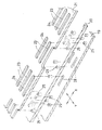
ヘッドユニット1は、 図2に示すように、前面( 図2における下面)に複数個のノズル11aを備えたキャビティユニット10と、その上面に対して接着剤または接着シートを介して接着し積層されるプレート型の圧電アクチュエータ12と、その背面(上面)に外部機器との電気的接続のために重ね接合された配線基板の1例としてのフレキシブルフラットケーブル40とにより構成されている。
The
キャビティユニット10は 図2に示すように構成されている。すなわち、下層から順にノズルプレート11、カバープレート15、ダンパープレート16、二枚のマニホールドプレート17,18、2枚のスペーサプレート19,20及び圧力室23が形成されているベースプレート21の合計8枚の偏平な板をそれぞれ接着剤にて接合して積層した構成である。合成樹脂製のノズルプレート11を除き、各プレート15〜21は、42%ニッケル合金鋼板製であり、それらの板厚を50μm〜150μm程度としている。
The cavity unit 10 is configured as shown in FIG. That is, in order from the lower layer, the
前記ノズルプレート11には、微小径(本実施形態では25μm程度)の多数のインク噴出用のノズル11aが、当該ノズルプレート11における第1の方向に沿って千鳥配列状に設けられている。また各ノズル列NはX方向に適宜間隔で5列(個別の列には、符号N1〜N5を付する、但し、N4,N5は図示せず)に配列されている。本実施形態では、第1列〜第5列の各々のノズル列Nの長さは1インチ、各々のノズル11aの数は75個で、つまり配列密度は75(dpi[ドット・パー・インチ])である。
Wherein the
そして、 図2において、右から順番にノズル列N1〜N5(但し、N4,N5は図示せず)とするとき、ノズル列N1はシアンインク(C)用であり、ノズル列N2はイエローインク(Y)用であり、ノズル列N3はマゼンタインク(M)用であり、ノズル列N4及びN5はブラックインク(BK)用とする。 In FIG. 2, when nozzle rows N1 to N5 are used in order from the right (where N4 and N5 are not shown), the nozzle row N1 is for cyan ink (C), and the nozzle row N2 is yellow ink ( Y), the nozzle row N3 is for magenta ink (M), and the nozzle rows N4 and N5 are for black ink (BK).
上下マニホールドプレート17,18には、Y方向に長いインク通路が各ノズル列N1〜N5に対応して板厚方向に貫通するように形成され、上側の第1スペーサプレート19と下側のダンパープレート16とに挟まれて積層されることにより、前記インク通路が5列の共通インク室(マニホールド室)26となる。そして、 図2において、右から順に共通インク室26a,26b,26c,26d,26eとするとき、共通インク室26aはシアンインク(C)用であり、共通インク室26bはイエローインク(Y)用であり、共通インク室26cはマゼンタインク(M)用であり、第4番目と第5番目の共通インク室26d,26eの対はブラックインク(BK)用となる。
In the upper and
図2において、ベースプレート21のY方向の一端部にX方向に適宜間隔で穿設された4つのインク供給口を右から順に符号31a,31b,31c,31dとするとき、インク供給口31a,31b,31cは、右端から順の共通インク室26a,26b,26cに対応し、右から4番目のインク供給口31dは、2つの共通インク室26d,26eの互いに近接した端部に共通に対応している。そして、 図2に示すように、インク供給口31a,31b,31cの位置に対応して、第2スペーサプレート20及び第1スペーサプレート91の一端部に穿設されたインク供給通路32が対応する共通インク室26a,26b,26cの一端部に連通している。
In FIG. 2, when four ink supply ports drilled at appropriate intervals in the X direction at one end portion in the Y direction of the
また、下側のマニホールドプレート17の下面に接着されるダンパープレート16の下面側には、各共通インク室26に対応する位置にY方向に長いダンパー室27が下面方向にのみ開放するように凹み形成され、その下面側のカバープレート15にて塞がれて完全な密閉状のダンパー室27が構成される。
Further, a
この構成により、圧電アクチュエータ12の駆動で圧力室23に作用する圧力波のうち、インクにより伝播されて共通インク室26の方向に向かう後退成分を、板厚の薄いダンパープレート16の振動により吸収し、いわゆるクロストークが発生することを防止するのである。
With this configuration, of the pressure waves acting on the
第1スペーサプレート19には、各ノズル列N1〜N5のノズル11aに対応する絞り部28がX方向に若干長く、Y方向に細幅の凹溝状に形成されている。この各絞り部28の一端は対応するマニホールドプレート18における共通インク室26a〜26eに連通し、各絞り部28の他端は後述するように、上側の第2スペーサプレート20における上下貫通する連通孔29に連通するように形成されている( 図3参照)。
The
カバープレート15、ダンパープレート16、2枚のマニホールド17,18、第1及び第2スペーサプレート19,20には、それぞれ、各ノズル列N1〜N5毎にノズル11aに連通する連通路25が、共通インク室26及びダンパー室27と上下に重ならない位置で上下に貫通するように形成されている。
The
また、ベースプレート21には、各ノズル列N毎に、X方向に沿って延びる細幅の圧力室23(各圧力室の列を符合23−1,23−2,23−3,23−4,23−5とする)がノズル11aの個数に対応してベースプレート21を厚さ方向に貫通して形成されている。そして、各圧力室23の長手方向(X方向)の一端は、第2スペーサプレート20に穿設された連通孔29を介して第1スペーサプレート19における各絞り部28の他端に連通しており、各圧力室23の長手方向の他端は、第2スペーサプレート20に穿設された各連通路25に連通している。各列の圧力室23は隔壁24を介してY方向に配置され、圧力室23は隣接する列の圧力室23に対してY方向に半ピッチずれ、いわゆる千鳥状に配列されている。
Further, the
これにより、各インク供給口31a〜31dから各共通インク通路26内に流入したインクは、絞り部28、連通孔29を通って各圧力室23内に分配されたのち、この各圧力室23内から連通路25を通って、この圧力室23に対応するノズル11aに至るという構成になっている。
As a result, the ink that has flowed into the common ink passages 26 from the
次に、圧電アクチュエータ12の構成について説明する。圧電アクチュエータ12は、後に詳述するように、圧電シートを積層方向に挟んで形成されている個別電極36とコモン電極37と間の前記圧電シートを活性部(エネルギー発生手段)として有し、任意の個別電極36とコモン電極37との間に電圧を印加することにより、その印加された個別電極36に対応した圧電シートの活性部に、当該積層方向に圧電縦効果による歪みを発生するものである。該活性部(エネルギー発生手段)は、圧力室23と対応する位置に形成されている。
Next, the configuration of the
即ち、前記活性部は、圧力室23の列方向(Y方向)に沿って並べられ、且つ前記圧力室23の列の数(5つ)と同じ数だけ、第2の方向(X方向)に並べられている。また、各活性部は、前記第2の方向(X方向)に圧力室23の長手方向に長く形成され、且つ隣接する活性部の配置間隔(ピッチP)も後述する圧力室23の配置と同様であって、千鳥状配列されることになる。
That is, the active portion are aligned along the column direction of the
圧電アクチュエータ12は、 図4に示すように、1枚の厚さが30μm程度の圧電セラミックス板からなる複数枚(本実施形態では7枚)の圧電シート33,34とが交互に積層された群と、この群の上面に1枚のシート46からなる拘束層を積層し、さらにその上面に表面シートとしてのトップシート35を積層した構造である。拘束層のシ−ト及びトップシ−トは圧電セラミックス板でも良いし、他の材料でも良く、電気的絶縁性を有すれば良い。
As shown in FIG. 4, the
最下層の圧電シート34から上方へ数えて偶数番目の圧電シート33の上面(平板面)には、 図4に示すように、前記キャビティユニット11における各圧力室23に対応した真上箇所ごとに細幅の個別電極36が、スクリーン印刷形成される。
On the upper surface (flat plate surface) of the even-numbered
図4は圧電シート33の一部のみを示し、前述した第1列〜第5列の圧力室列23−1,23−2,23−3,23−4,23−5に対応して第1列目〜第5列目の個別電極36(各列に対して、 図4で符号36−1、36−2、36−3、36−4、36−5を付する)が形成されている。各個別電極36の直線部36bは、前記各圧力室23( 図6の点線参照)とほぼ同じ長さで平面視で重複しており、且つ各圧力室よりもやや狭い幅の直線状に形成されている( 図7(a)参照)。
FIG. 4 shows only a part of the
各個別電極36における一端部36aは、 図7(a)に示すように、それぞれ平面視で直線部36bに対して屈曲形成されて、圧力室23の外に延びている。なお、第3列目の個別電極36−3における一端部36aは、 図4に示すように、圧力室23の外側一端に対して交互に外に延びている。
As shown in FIG. 7A, one end portion 36 a of each
また、この各端部36aは、上下に隣接する圧電シート34における第1の島状個別導通部としてのダミー個別電極38及び後述する拘束層シート46の接続パターン53とそれぞれ少なくとも一部が平面視で重なり( 図4、 図7(a)参照)、圧電シート34及び拘束層シート46を貫通するスルーホール状の内部導通電極42とそれぞれ電気的に接続可能な位置に配置される。
Further, the each end 36a includes a
さらに、圧電シート33には、圧電シート34におけるコモン電極37と平面視で一部重複する個所であって、圧電シート33の平板面における短辺及び長辺に沿う外周部位等にダミーコモン電極43が形成されている( 図4参照)。
Furthermore, the
コモン電極37は、最下層の圧電シート34とそれから上方へ数えて奇数番目の圧電シート34の各上面(平板面)にスクリーン印刷形成されるものである( 図4参照)。最下層の圧電シート34におけるコモン電極37は当該圧電シート34の上面全体に形成されている。それより上層の各圧電シート34におけるコモン電極37は、各圧力室列23−1〜23−5ひいては各個別電極列36−1〜36−5の配置位置と平面視で重複し、且つ圧電シート34の長辺に沿ってY方向に長い第1電気導通部分37aと、圧電シート34の短辺に沿ってX方向に長く、第1電気導通部分37aの両端に連結する第2電気導通部分37bとからなる。コモン電極37はこれら圧電シート34に形成される島状のダミー個別電極38の列部分を囲んで形成されている。
The
平面視略矩形状の各ダミー個別電極38は、各個別電極36の直線部36bではなく、各一端部36aの少なくとも一部と平面視で重複するように一定間隔で配置形成されている。
The dummy
拘束層シート46の上面には、 図4に示すように、平面視で略矩形型の接続用パターン53が前記圧電シート34における各ダミー個別電極38の少なくとも一部と平面視で重複するように一定間隔で配置形成されている。また、拘束層シート46の上面の短辺に沿う部位等には、圧電シ−ト34におけるコモン電極37の一部及び圧電シ−ト33におけるダミーコモン電極43の一部にそれぞれ平面視で重複する位置にコモン導通部としての連絡用パターン54が形成されている。
The upper surface of the restraint Soshi over
そして、最下層の圧電シート34を除き、それより上層の圧電シート34、33及び拘束層シート46には、電気導通部分37a,37bとダミーコモン電極43との複数箇所を上下方向に電気的に接続するために、電極37、43の位置において、各圧電シート34、33の板厚を貫通するように穿設された複数のスルーホール内にそれぞれ充填した導電部材(導電性ペースト)にて内部導通電極(図示せず)を形成する。同様に、複数枚の圧電シート33における各個別電極36の端部36aと、圧電シート34における各ダミー個別電極38と、拘束層シート46における連絡用パターン54には、それぞれを上下方向に電気的に接続するために、各圧電シート33、34、46の板厚を貫通するように穿設された複数のスルーホール内にそれぞれ充填した導電部材(導電性ペースト)にて内部導通電極42が形成されている。その場合、各内部導通電極42は、上下に隣接する圧電シート33、34、46で平面視で上下に重複しない位置に適宜距離だけ隔てて形成されている( 図6、 図7(a)参照)。
Except for the lowermost
図4〜 図7に示すように、圧電アクチュエータ12の最上層である表面シートとしてのトップシ−ト35の上面(平坦面)には、フレキシブルフラットケーブル40の後述する接合電極部77、78とそれぞれ接合させるためのコモン電極接続用の接合端子90及び個別電極接続用の接合端子91とがそれぞれ島状に形成されている。
As shown in FIGS. 4 to 7, on the upper surface ( flat surface) of the
接合端子90及び接合端子91は、それぞれ、トップシ−ト35の表面上に形成される層厚の薄い表面電極92及び93と、その表面電極92及び93の表面上に形成される層厚の厚い外部電極94及び95とからなる。トップシ−ト35の接合端子90及び接合端子91と、対応する拘束層シート46の連絡用パターン54及び接続用パターン53とを、それぞれ上下方向に電気的に接続するために、前記と同様に、トップシ−ト35の板厚を貫通するように穿設された複数のスルーホール内にそれぞれ充填した導電部材(導電性ペースト)にて内部導通電極44が形成されている。
Connecting
表面電極92及び93は、トップシート35の元材料であるグリーンシートの表面にスクリーン印刷形成される。個別電極36、コモン電極37、ダミー個別電極38、ダミーコモン電極43、スルーホール内に充填する内部導通電極42,44、接続用パターン53、連絡用パターン54及び表面電極92及び93を、銀−パラジュウム系導電部材(導電性ペースト)を用いて圧電シート33、34、拘束層シート46及びトップシート35の元材料であるグリーンシートの表面にスクリーン印刷形成した後、それらシートを所定の順に積層し,さらに焼成してアクチュエータ12が形成される。銀−パラジュウム系導電部材は融点が高いため、焼成温度が高温となるグリーンシートの焼成が行われても蒸発することがないが、半田合金との接合性は良くない。
The
外部電極94及び95は銀−ガラスフリット系の厚膜用の導電性ペーストを用いて前記焼成後に表面電極92及び93の表面に印刷形成した後に前記焼成温度より低い温度で焼成して形成される。銀−ガラスフリット系の導電部材は、銀−パラジュウム系導電部材に比べると、融点は低いが半田合金との接合性は良好である。従って、接合端子90,91は、表面電極92及び93の表面上に外部電極94及び95が形成されることによって、外部電極94及び95が形成されない場合に比べてバンプ電極103との接合性が向上する。
The
個別電極接続用の接合端子91の構成をさらに詳述すると、トップシ−ト35の上面には、拘束層シ−ト46における各接続用パターン53にそれぞれ平面視で少なくとも一部が重複するように、層厚の薄い表面電極93が一定間隔で配置形成されている。この各表面電極93は、 図6、 図7(a)及び 図7(b)に示すように、トップシ−ト35の短辺縁(X方向と平行な縁)ひいては各個別電極36における各直線部36bと略平行であって、 図7(b)に示すように、その各下方に並列状に位置する相隣接する圧力室23、23の間の隔壁24の上方に配置されている。従って、表面電極93は、圧力室23の第1の方向の配置間隔Pと同じ間隔にて、かつそれと半ピッチずれて配列され、圧力室の各列と対応して第2の方向に複数列配置されることになる。そして、表面電極93の大部分は隔壁24の幅寸法W1よりも狭い幅寸法W2(W2<W1)を有する細幅部93aであり、この細幅部93aに連接して広幅部93bが形成される。広幅部93bの幅寸法W3は隔壁24の幅寸法W1より若干広く設定されている。本実施形態では、P=0.339μm 、W1= 120μm 〜 150μm 、W2= 100μm 、W3= 150〜300 μm 程度であり、W3= 200〜220 μm 程度が好ましい。広幅部93bの長さ寸法L3= 360μm 程度である。また、表面電極93の層厚は1〜2μm 程度である。
More specifically the joining pin 9 1 configuration for the individual electrodes connected Toppushi - on the upper surface of the
表面電極93は、図7に示すように、列方向(Y方向)において交互に、広幅部93bと細幅部93aとが反対方向に位置するように配置される。内部導通電極44は、各列の表面電極93の一端側に接続されるため、列方向に広幅部93bと細幅部93aとに交互に接続されることになる。外部電極95は、各広幅部93bの表面に付着され、列方向に1つおきの内部導通電極44の上方に位置し、且つ表面電極93の両端に交互に、すなわち千鳥配列状に位置することになる。そして、外部電極95の平面視の大きさは広幅部93bの面積よりも小さく、且つ外部電極95の平面視の周縁が広幅部93bの周縁よりも内周側に位置するように配置されている。本実施形態では外部電極95の幅寸法W4≒ 150〜 200μm 程度であり、外部電極95の周縁と広幅部93bの周縁との間の平面視の間隔寸法W5が25μm 程度あることが望ましい( 図9(a)参照)。外部電極95の層厚は20μm である。
As shown in FIG. 7, the
同様に、コモン電極接続用の接合端子90における層厚の薄い表面電極92は、拘束層シ−ト46における連絡用パターン54の少なくとも一部に平面視で重複するように配置され、且つトップシ−ト35の上面のうち外周縁寄り部位に帯状等にて形成されている( 図4参照)。また、表面電極92の表面に後付けとしての層厚の厚い外部電極94を適宜形状にて配置する。
Similarly, the
個別電極用の接合端子91において、図6及び図7(b)に示すように、表面電極93の、内部導通電極44と接続する箇所に充填電極96が形成される。つまり、表面電極の広幅部93b上の外部電極95は、充填電極96を兼用することになり、表面電極の列方向に外部電極95と充填電極96とが交互に位置することになる。充填電極96は、内部導通電極42,44が表面電極92,93と接続する箇所が圧電アクチュエータ20の上面として外部に露出するので、各スルーホール部分を含めて内部導通電極42,44の上面部位を前記外部電極94及び95と同じ材料で充填することにより、内部導通電極42,44と表面電極92,93との接続箇所を保護することができる。なお、上記のようにY方向に接合端子91の広幅部93bと細幅部93aとが交互に形成されることから、広幅部93bを有するように接合端子91を形成したとしても、Y方向において、隣接する2つの接合端子91間の間隔を充分に確保することができ、これらが電気的に短絡する危険性を少なくすることができる。これら充填電極96、外部電極94及び95は平面視矩形状、小判型または楕円状等の適宜形状を採用し得る。
次に、フレキシブルフラットケーブル40の構成について、 図8(a)及び 図8(b)を参照しながら説明する。
フレキシブルフラットケーブル40は、トップシート35の上面に重ねられ、ノズル列と直交する方向(X方向)に外方へ突出して配置される( 図1参照)。フレキシブルフラットケーブル40は、帯状のベース材100と、その片面に形成された配線79及びコモン電極用の接合電極部77、個別電極用の接合電極部78と、これらの表面を被覆するカバーレイ101とで構成されている。ベース材100及びカバーレイ101は、電気絶縁性を有し、可撓性の合成樹脂材(例えば、ポリイミド樹脂、ポリエステル樹脂、ポリアミド樹脂)からなる。接合電極部77,7及び配線79はベース材100の片面に銅箔にてフォトレジスト法等により形成されている。配線79はベース材100に搭載された駆動用の集積回路102に電気的に接合されている。フレキシブルフラットケーブル40の外方へ突出した端部に設けられた複数の端子105は、集積回路102と接続されている。なお、島状の個別電極用の接合電極部78は、トップシート35上の接合端子91の外部電極95とそれぞれ対面する位置にあって、その対面する部位のベース材100に開けられた孔(開口部)の部位に半田合金からなるバンプ電極103を固着している( 図8(b)参照)。同様に、帯状のコモン電極用の接合電極部77(後述する77−1及び77−2)のうち、トップシート35上の接合端子90の外部電極94とそれぞれ対面する箇所に開けられた孔(開口部)の部位にバンプ電極103を固着している。
In the
Next, the configuration of the full lexical flat cable 4 0 will be described with reference to FIGS. 8 (a) and 8 (b).
The flexible
コモン電極用接合電極部77は、図8(a)に示すように、第2の方向(X方向)に沿って延びるフレキシブルフラットケーブル40の対の側縁に沿って形成された帯状の2本の第1コモン接合電極部77−1を少なくとも有する。また、第1の方向(Y方向)に沿って延びる側縁に沿って形成された帯状の1本の第2コモン接合電極部77−2を有し、さらに、第2コモン接合電極部77−2の両端が各第1コモン接合電極部77−1の先端部に電気的に接続されている。2本の第1コモン接合電極部77−1の他端部は、フレキシブルフラットケーブル40の外方へ突出した端部に設けられた接続端子104に電気的に接続されている。
他方、個別電極用接合電極部78は、各列の外部電極95に対向して配置されている。 即ち、前述のとおり外部電極95は表面電極23の各列において表面電極23の両端に交互に配列されているため、接合電極部78もこれに対応して千鳥状に配列された群をなし、図8(a)に示すように、表面電極23の複数列(つまり圧力室の列23−1〜23−5と対応した列)に対応して複数の群78−1〜78−5をなしている。
On the other hand, the individual
そして、全ての列の各個別電極用接合電極部78に接続する配線79は、第2の方向(X方向)に沿って延びる配線パターンにて形成されている。
The
駆動用の集積回路102は、外部機器(画像形成装置本体の制御基板)からシリアル転送されてくる記録データを、各ノズルに対応するパラレルデータに変換し、かつ記録データに対応した所定電圧の波形信号を生成して、各配線79に出力するものである。集積回路102とアクチュエータ12との間の接続は、ノズル数に対応した配線79を高密度に形成する必要があるが、集積回路102よりも制御基板側では、記録データをシリアル転送するので、低密度な配線パターンでよい。
The driving
半田合金製のバンプ電極103は、コモン電極用接合端子90の外部電極94及び個別電極用接合端子91の外部電極95にそれぞれ重ねて加熱押圧して接合される。その場合、 図9(b)に示すように、バンプ電極103の溶融した半田合金は、外部電極95の上面及び側面を覆い、且つ表面電極93における広幅部93bの表面を周縁近傍まで覆う。そして、銀−パラジュウム系の表面電極93の広幅部93bの表面は溶融した半田合金との濡れ性が大きい一方、銀−ガラスフリット系の外部電極95と半田合金とは共晶結合して接合強度は高い。なお、半田合金の量が多く、広幅部93bから溢れ出した場合は、細幅部93aに流れ込んで固化するので、隣接する表面電極93との間で電気的に短絡(ショート)する危険性は少ない。
Solder
外部電極95の周縁から広幅部93bの周縁までの寸法W5が大きいと、外部電極95の周縁と広幅部93bの表面との間の隅肉部(フィレット)103a( 図9(b)参照)の断面の半径を大きくでき、材料力学でいう圧力集中係数(形状係数)を小さくできる。従って、温度変化の大きいもとでの繰り返し使用により、フレキシブルフラットケーブル40が大きく伸縮して、バンプ電極103の間隔が伸縮し、これに接合されている外部電極95との間の隅肉部(フィレット)103aに大きい応力集中が作用した場合や繰り返し応力を受けても、隅肉部103aに亀裂が発生難いから電気的断線事故も発生しないのである。
When peripheral or found wide portion dimension W5 of the peripheral or the 93b
なお、前記応力集中は、フレキシブルフラットケーブル40の幅方向(Y方向)の収縮時に大きくなるので、これに耐久性を持たせるためには、上記のように、隅肉部103aが形成される土台(領域)となる広幅部93bの幅寸法W5を大きくすることが望ましいのである。
The stress concentration increases when the flexible
個別電極用の接合端子91ひいては表面電極93及び外部電極95を、キャビティユニット10における圧力室23の配列の間、即ち隔壁24上に相当する箇所に配置すれば、フレキシブルフラットケーブル40のバンプ電極103を外部電極95と対面させて押圧するとき、隔壁24にて押圧力を支持でき、空洞である圧力室23の変形を防止できるという効果を奏する。
The
前記実施形態では、ノズルの列は5列ひいては個別電極用接合電極78が千鳥配列で10列であったが、本発明では3列以上の個別電極用接合電極78に対して適用できるものである。
In the above-described embodiment, the number of nozzles is five, and the individual
1 インクジェット記録ヘッド
11 キャビティユニット
11a ノズル
12 圧電アクチュエータ
22 ベースプレート
23 圧力室
33,34 圧電シート
35 トップシート
36 個別電極
37 コモン電極
40 フラットケーブル
53 接続用パターン
54 連絡用パターン
77 コモン電極用の接合電極部
78 個別電極用の接合電極部
79 配線
90 コモン電極用接合端子
91 個別電極用接合端子
92、93 表面電極
94、95 外部電極
102 集積回路
103 バンプ電極
103a 隅肉部
DESCRIPTION OF
Claims (11)
前記配線基板は、溶融可能なバンプ電極を前記接合端子と重ね接合される位置に備え、
前記接合端子は、前記アクチュエータの表面に形成した表面電極と、該表面電極の表面上に突出して形成され、前記バンプ電極との接合性が前記表面電極よりも良い外部電極とからなり、
前記表面電極は、第1の方向に並んで配列されるとともに、その第1の方向と直交する第2の方向に前記外部電極よりも長く形成され、かつ一端に平面視において前記各外部電極を囲む周縁を有する広幅部を有するとともに、該広幅部から前記第2の方向に延び該広幅部よりも前記第1の方向の幅を狭くした細幅部を有し、
前記複数の表面電極は、該表面電極の前記広幅部と前記細幅部とが交互に逆向きに位置するように、前記第1の方向に配置されているとともに、前記外部電極は、前記各表面電極の広幅部上に配置され、
前記バンプ電極は、溶融した後固化した状態で、前記外部電極及び前記表面電極を覆っていることを特徴とするインクジェット記録ヘッドにおける配線基板の接合構造。 A plurality of nozzles arranged in a line along the first direction, a pressure chamber corresponding to each nozzle, and a plurality of energy generating means for selectively ejecting ink corresponding to each pressure chamber Inkjet recording comprising: an actuator having a plurality of junction terminals arranged in an island shape corresponding to each of the energy generating means on the surface of the actuator ; and a wiring board that outputs a waveform signal of a predetermined voltage from a circuit element A bonding structure for connecting the wiring board to the bonding terminal in the head ;
The wiring board is provided with a meltable bump electrode at a position where it is overlapped with the joining terminal ,
The bonding terminal is formed of a surface electrode formed on the surface of the actuator, and an external electrode that is formed to protrude on the surface of the surface electrode, and the bonding property with the bump electrode is better than the surface electrode .
The surface electrodes are arranged side by side in a first direction, are formed longer than the external electrodes in a second direction orthogonal to the first direction, and each external electrode is arranged at one end in a plan view. Having a wide portion having a peripheral edge, and having a narrow portion extending from the wide portion in the second direction and having a narrower width in the first direction than the wide portion,
The plurality of surface electrodes are arranged in the first direction such that the wide portions and the narrow portions of the surface electrodes are alternately positioned in opposite directions, and the external electrodes are arranged in the respective directions. Arranged on the wide part of the surface electrode,
The bonding structure of a wiring board in an ink jet recording head , wherein the bump electrode covers the external electrode and the surface electrode in a state of being solidified after being melted .
前記複数の表面電極は、各表面電極の列ごとに、該表面電極の前記広幅部と前記細幅部とが交互に逆向きに位置するように、前記第1の方向に配置されていることを特徴とする請求項1に記載のインクジェット記録ヘッドにおける配線基板の接合構造。 It said ink jet recording head, a row of pressure chambers corresponding to Bruno row of nozzle and its ing from a plurality of nozzles arranged in a row along the first direction, together comprise a plurality of rows in the second direction, Corresponding to the row of the plurality of pressure chambers, a plurality of energy generating means are provided, and the surface electrode connected to the plurality of energy generating means is provided on the surface of the actuator,
The plurality of surface electrodes are arranged in the first direction so that the wide portions and the narrow portions of the surface electrodes are alternately positioned in opposite directions for each row of the surface electrodes. The junction structure of a wiring board in an ink jet recording head according to claim 1.
前記バンプ電極は、前記外部電極の上面及び側面を覆い、前記広幅部の表面を周縁近傍まで覆っていることを特徴とする請求項1または2に記載のインクジェット記録ヘッドにおける配線基板の接合構造。 The external electrode is disposed on the surface of the wide portion so that the peripheral edge of the external electrode is positioned on the inner peripheral side of the peripheral edge of the wide portion,
3. The wiring board bonding structure according to claim 1 , wherein the bump electrode covers an upper surface and a side surface of the external electrode, and covers a surface of the wide portion to a vicinity of a peripheral edge .
前記バンプ電極を前記外部電極に重ねて加熱押圧することで、該バンプ電極を溶融して、前記外部電極及び前記表面電極を覆った状態で固化させることを特徴とするインクジェット記録ヘッドにおける配線基板の接合方法。 The bonding method of the wiring board, wherein the wiring board is connected to the bonding terminal in the bonding structure of the wiring board in the inkjet recording head according to claim 1,
The bump electrode is heated and pressed over the external electrode to melt the bump electrode and solidify it while covering the external electrode and the surface electrode. Joining method .
該シートの元材料であるグリーンシートの表面に、前記表面電極を印刷形成した後焼成し、該焼成した前記表面電極の表面に、前記外部電極を印刷形成した後、前記焼成温度よりも低い温度で焼成することを特徴とする請求項9に記載のインクジェット記録ヘッドにおける配線基板の接合方法。 The actuator includes a plurality of stacked sheets including a piezoelectric sheet,
The surface electrode is printed on the surface of the green sheet, which is the original material of the sheet, and then fired. After the external electrode is printed on the surface of the fired surface electrode, the temperature is lower than the firing temperature. The method for bonding wiring boards in an ink jet recording head according to claim 9, wherein the wiring board is fired.
Priority Applications (3)
| Application Number | Priority Date | Filing Date | Title |
|---|---|---|---|
| JP2004015494A JP4161213B2 (en) | 2004-01-23 | 2004-01-23 | Wiring board bonding structure in ink jet recording head and bonding method thereof |
| US11/040,744 US7416279B2 (en) | 2004-01-23 | 2005-01-21 | Connection structure for inkjet recording head |
| US11/171,929 US7517065B2 (en) | 2004-01-23 | 2005-06-29 | Injet printhead having externally-connected terminations structured to be resistant to damage |
Applications Claiming Priority (1)
| Application Number | Priority Date | Filing Date | Title |
|---|---|---|---|
| JP2004015494A JP4161213B2 (en) | 2004-01-23 | 2004-01-23 | Wiring board bonding structure in ink jet recording head and bonding method thereof |
Publications (3)
| Publication Number | Publication Date |
|---|---|
| JP2005205769A JP2005205769A (en) | 2005-08-04 |
| JP2005205769A5 JP2005205769A5 (en) | 2008-07-17 |
| JP4161213B2 true JP4161213B2 (en) | 2008-10-08 |
Family
ID=34792439
Family Applications (1)
| Application Number | Title | Priority Date | Filing Date |
|---|---|---|---|
| JP2004015494A Expired - Lifetime JP4161213B2 (en) | 2004-01-23 | 2004-01-23 | Wiring board bonding structure in ink jet recording head and bonding method thereof |
Country Status (2)
| Country | Link |
|---|---|
| US (1) | US7416279B2 (en) |
| JP (1) | JP4161213B2 (en) |
Families Citing this family (17)
| Publication number | Priority date | Publication date | Assignee | Title |
|---|---|---|---|---|
| JP4507170B2 (en) * | 2004-02-23 | 2010-07-21 | ブラザー工業株式会社 | Inkjet printer head |
| US7525240B2 (en) | 2004-04-26 | 2009-04-28 | Tdk Corporation | Electronic component |
| JP4940672B2 (en) * | 2006-01-27 | 2012-05-30 | ブラザー工業株式会社 | Inkjet recording head |
| JP4934325B2 (en) * | 2006-02-17 | 2012-05-16 | 株式会社フジクラ | Printed wiring board connection structure and printed wiring board connection method |
| JP5194385B2 (en) * | 2006-06-03 | 2013-05-08 | ブラザー工業株式会社 | Multilayer piezoelectric actuator and manufacturing method thereof |
| JP5526464B2 (en) * | 2006-06-03 | 2014-06-18 | ブラザー工業株式会社 | Multilayer piezoelectric actuator |
| JP5194386B2 (en) * | 2006-06-03 | 2013-05-08 | ブラザー工業株式会社 | Multilayer piezoelectric actuator |
| US7497558B2 (en) * | 2006-06-03 | 2009-03-03 | Brother Kogyo Kabushiki Kaisha | Piezoelectric actuator and liquid-droplet jetting head |
| JP5034593B2 (en) * | 2007-03-26 | 2012-09-26 | ブラザー工業株式会社 | Structure of wiring board with drive circuit and droplet discharge head |
| JP5006680B2 (en) * | 2007-03-30 | 2012-08-22 | キヤノン株式会社 | Ink jet recording head and method of manufacturing ink jet recording head |
| US8104860B2 (en) * | 2007-09-28 | 2012-01-31 | Brother Kogyo Kabushiki Kaisha | Ink-jet recording apparatus including abnormality judging portion |
| JP2009094120A (en) * | 2007-10-04 | 2009-04-30 | Brother Ind Ltd | Piezoelectric actuator, droplet discharge head using the same, and method of manufacturing piezoelectric actuator |
| JP5180975B2 (en) * | 2008-02-18 | 2013-04-10 | セイコーインスツル株式会社 | Piezoelectric vibrator manufacturing method and piezoelectric vibrator |
| JP5157989B2 (en) * | 2009-03-26 | 2013-03-06 | ブラザー工業株式会社 | Piezoelectric actuator and droplet discharge head using the same |
| JP5126208B2 (en) * | 2009-11-30 | 2013-01-23 | ブラザー工業株式会社 | Piezoelectric actuator, liquid discharge head, method for manufacturing piezoelectric actuator, and method for manufacturing liquid discharge head |
| JP6942607B2 (en) * | 2017-10-30 | 2021-09-29 | キヤノン株式会社 | Liquid discharge head and its manufacturing method |
| JP7106938B2 (en) * | 2018-03-30 | 2022-07-27 | ブラザー工業株式会社 | liquid ejection head |
Family Cites Families (25)
| Publication number | Priority date | Publication date | Assignee | Title |
|---|---|---|---|---|
| US5912684A (en) * | 1990-09-21 | 1999-06-15 | Seiko Epson Corporation | Inkjet recording apparatus |
| US5315472A (en) * | 1991-07-23 | 1994-05-24 | Hewlett Packard Company | Ground ring/spark gap ESD protection of tab circuits |
| DE69329041T2 (en) * | 1993-04-30 | 2001-03-22 | Hewlett-Packard Co., Palo Alto | Carriage assembly to hold two inkjet cartridges |
| US6003974A (en) * | 1993-04-30 | 1999-12-21 | Hewlett-Packard Company | Unitary interconnect system for an inkjet printer |
| DE69412915T2 (en) * | 1993-06-16 | 1999-04-01 | Seiko Epson Corp., Tokio/Tokyo | Ink jet recorder |
| US5644341A (en) * | 1993-07-14 | 1997-07-01 | Seiko Epson Corporation | Ink jet head drive apparatus and drive method, and a printer using these |
| US5818473A (en) * | 1993-07-14 | 1998-10-06 | Seiko Epson Corporation | Drive method for an electrostatic ink jet head for eliminating residual charge in the diaphragm |
| JPH09109394A (en) * | 1995-10-18 | 1997-04-28 | Canon Inc | Recording head |
| US6062675A (en) * | 1996-01-09 | 2000-05-16 | Canon Kabushiki Kaisha | Recording head, recording apparatus and manufacturing method of recording head |
| JPH10211701A (en) * | 1996-11-06 | 1998-08-11 | Seiko Epson Corp | Actuator with piezoelectric element, ink jet type recording head, and manufacture of them |
| JPH10217461A (en) * | 1997-02-06 | 1998-08-18 | Minolta Co Ltd | Ink jet recorder |
| JPH11320873A (en) * | 1997-06-05 | 1999-11-24 | Ricoh Co Ltd | Ink-jet head |
| JPH11147311A (en) | 1997-11-17 | 1999-06-02 | Fujitsu Ltd | Ink-jet recording head |
| US6454394B2 (en) * | 2000-03-21 | 2002-09-24 | Olympus Optical Co., Ltd. | Inkjet head which prevents transfer of a load applied to an inkjet-head-side connector |
| JP2002103691A (en) * | 2000-10-05 | 2002-04-09 | Fuji Photo Film Co Ltd | Gray scale reproducing method and gray scale reproduction image |
| JP2003165212A (en) * | 2001-11-30 | 2003-06-10 | Brother Ind Ltd | Ink jet head |
| JP3767395B2 (en) | 2001-03-01 | 2006-04-19 | ブラザー工業株式会社 | Manufacturing method of multilayer piezoelectric element |
| US6595628B2 (en) * | 2001-02-19 | 2003-07-22 | Brother Kogyo Kabushiki Kaisha | Laminated piezoelectric element for use as a drive device |
| US7149090B2 (en) * | 2001-09-11 | 2006-12-12 | Brother Kogyo Kabushiki Kaisha | Structure of flexible printed circuit board |
| JP2003159795A (en) | 2001-09-11 | 2003-06-03 | Brother Ind Ltd | Recording apparatus |
| US6619787B2 (en) * | 2001-10-31 | 2003-09-16 | Hewlett-Packard Development Company, L.P. | Limiting unwanted ink penetration of flexible circuits of fluid ejection devices |
| JP4296738B2 (en) * | 2001-11-30 | 2009-07-15 | ブラザー工業株式会社 | Inkjet head |
| JP3861673B2 (en) * | 2001-11-30 | 2006-12-20 | ブラザー工業株式会社 | Inkjet recording head |
| US6971738B2 (en) * | 2001-12-06 | 2005-12-06 | Brother Kogyo Kabushiki Kaisha | Piezoelectric actuator |
| JP3922151B2 (en) * | 2002-09-27 | 2007-05-30 | ブラザー工業株式会社 | Flexible wiring board connection structure and connection method |
-
2004
- 2004-01-23 JP JP2004015494A patent/JP4161213B2/en not_active Expired - Lifetime
-
2005
- 2005-01-21 US US11/040,744 patent/US7416279B2/en active Active
Also Published As
| Publication number | Publication date |
|---|---|
| US7416279B2 (en) | 2008-08-26 |
| JP2005205769A (en) | 2005-08-04 |
| US20050162484A1 (en) | 2005-07-28 |
Similar Documents
| Publication | Publication Date | Title |
|---|---|---|
| US7416279B2 (en) | Connection structure for inkjet recording head | |
| US7517065B2 (en) | Injet printhead having externally-connected terminations structured to be resistant to damage | |
| US7294952B2 (en) | Laminated-type piezoelectric element and inkjet recording head having the same | |
| JP2005205769A5 (en) | ||
| US7900355B2 (en) | Ink-jet head and method for manufacturing the same | |
| JP4419754B2 (en) | Inkjet head | |
| US7469994B2 (en) | Ink-jet head and connecting structure | |
| JP4940672B2 (en) | Inkjet recording head | |
| JP5211631B2 (en) | Droplet discharge apparatus and manufacturing method thereof | |
| JP4379583B2 (en) | Inkjet recording head | |
| JP4552671B2 (en) | Substrate assembly, inkjet head, and manufacturing method thereof | |
| JP4882083B2 (en) | Assembling method of inkjet head | |
| JP2007203481A (en) | Inkjet type recording head | |
| JP2007203482A (en) | Inkjet printer head and head unit | |
| US8083331B2 (en) | Piezoelectric actuator, liquid ejection head, and method for manufacturing piezoelectric actuator | |
| JP2006231913A (en) | Ink jet head and a connecting structure of flexible wiring board and terminal forming member | |
| JP4221596B2 (en) | Bonding structure of flexible flat cable in inkjet recording head | |
| JP5526464B2 (en) | Multilayer piezoelectric actuator | |
| JP5157989B2 (en) | Piezoelectric actuator and droplet discharge head using the same | |
| JP2006015539A5 (en) | ||
| JP3885696B2 (en) | Inkjet head | |
| JP2005280044A (en) | Process of manufacturing inkjet head | |
| JP5194385B2 (en) | Multilayer piezoelectric actuator and manufacturing method thereof | |
| JP2010201870A (en) | Joint structure of wiring board and method of manufacturing the joint structure | |
| JP5194386B2 (en) | Multilayer piezoelectric actuator |
Legal Events
| Date | Code | Title | Description |
|---|---|---|---|
| A621 | Written request for application examination |
Free format text: JAPANESE INTERMEDIATE CODE: A621 Effective date: 20061227 |
|
| A521 | Request for written amendment filed |
Free format text: JAPANESE INTERMEDIATE CODE: A523 Effective date: 20080530 |
|
| TRDD | Decision of grant or rejection written | ||
| A01 | Written decision to grant a patent or to grant a registration (utility model) |
Free format text: JAPANESE INTERMEDIATE CODE: A01 Effective date: 20080625 |
|
| A01 | Written decision to grant a patent or to grant a registration (utility model) |
Free format text: JAPANESE INTERMEDIATE CODE: A01 |
|
| A61 | First payment of annual fees (during grant procedure) |
Free format text: JAPANESE INTERMEDIATE CODE: A61 Effective date: 20080708 |
|
| FPAY | Renewal fee payment (event date is renewal date of database) |
Free format text: PAYMENT UNTIL: 20110801 Year of fee payment: 3 |
|
| R150 | Certificate of patent or registration of utility model |
Free format text: JAPANESE INTERMEDIATE CODE: R150 Ref document number: 4161213 Country of ref document: JP Free format text: JAPANESE INTERMEDIATE CODE: R150 |
|
| FPAY | Renewal fee payment (event date is renewal date of database) |
Free format text: PAYMENT UNTIL: 20120801 Year of fee payment: 4 |
|
| FPAY | Renewal fee payment (event date is renewal date of database) |
Free format text: PAYMENT UNTIL: 20120801 Year of fee payment: 4 |
|
| FPAY | Renewal fee payment (event date is renewal date of database) |
Free format text: PAYMENT UNTIL: 20130801 Year of fee payment: 5 |
|
| EXPY | Cancellation because of completion of term |