JP4161213B2 - インクジェット記録ヘッドにおける配線基板の接合構造及びその接合方法 - Google Patents
インクジェット記録ヘッドにおける配線基板の接合構造及びその接合方法 Download PDFInfo
- Publication number
- JP4161213B2 JP4161213B2 JP2004015494A JP2004015494A JP4161213B2 JP 4161213 B2 JP4161213 B2 JP 4161213B2 JP 2004015494 A JP2004015494 A JP 2004015494A JP 2004015494 A JP2004015494 A JP 2004015494A JP 4161213 B2 JP4161213 B2 JP 4161213B2
- Authority
- JP
- Japan
- Prior art keywords
- electrode
- wiring board
- electrodes
- recording head
- bonding
- Prior art date
- Legal status (The legal status is an assumption and is not a legal conclusion. Google has not performed a legal analysis and makes no representation as to the accuracy of the status listed.)
- Expired - Lifetime
Links
- 238000000034 method Methods 0.000 title claims description 10
- 230000002093 peripheral effect Effects 0.000 claims description 26
- 239000004020 conductor Substances 0.000 claims description 14
- 238000010304 firing Methods 0.000 claims description 13
- SWELZOZIOHGSPA-UHFFFAOYSA-N palladium silver Chemical compound [Pd].[Ag] SWELZOZIOHGSPA-UHFFFAOYSA-N 0.000 claims description 13
- 239000000463 material Substances 0.000 claims description 11
- 239000011521 glass Substances 0.000 claims description 9
- 238000005192 partition Methods 0.000 claims description 9
- 238000010030 laminating Methods 0.000 claims description 4
- 238000000638 solvent extraction Methods 0.000 claims description 3
- 239000000976 ink Substances 0.000 description 56
- 229910045601 alloy Inorganic materials 0.000 description 12
- 239000000956 alloy Substances 0.000 description 12
- 229910000679 solder Inorganic materials 0.000 description 12
- 125000006850 spacer group Chemical group 0.000 description 10
- 238000002844 melting Methods 0.000 description 7
- 230000008018 melting Effects 0.000 description 7
- 239000000758 substrate Substances 0.000 description 7
- 238000004891 communication Methods 0.000 description 5
- KDLHZDBZIXYQEI-UHFFFAOYSA-N Palladium Chemical compound [Pd] KDLHZDBZIXYQEI-UHFFFAOYSA-N 0.000 description 4
- 238000007650 screen-printing Methods 0.000 description 4
- 239000000853 adhesive Substances 0.000 description 3
- 230000001070 adhesive effect Effects 0.000 description 3
- 230000008602 contraction Effects 0.000 description 3
- 238000003825 pressing Methods 0.000 description 3
- 229920003002 synthetic resin Polymers 0.000 description 3
- 239000000057 synthetic resin Substances 0.000 description 3
- BQCADISMDOOEFD-UHFFFAOYSA-N Silver Chemical compound [Ag] BQCADISMDOOEFD-UHFFFAOYSA-N 0.000 description 2
- 239000000919 ceramic Substances 0.000 description 2
- 238000010438 heat treatment Methods 0.000 description 2
- 229910052763 palladium Inorganic materials 0.000 description 2
- 229910052709 silver Inorganic materials 0.000 description 2
- 239000004332 silver Substances 0.000 description 2
- RYGMFSIKBFXOCR-UHFFFAOYSA-N Copper Chemical compound [Cu] RYGMFSIKBFXOCR-UHFFFAOYSA-N 0.000 description 1
- 229910000990 Ni alloy Inorganic materials 0.000 description 1
- 229910000831 Steel Inorganic materials 0.000 description 1
- 230000004888 barrier function Effects 0.000 description 1
- 229910010293 ceramic material Inorganic materials 0.000 description 1
- 239000011889 copper foil Substances 0.000 description 1
- 230000000694 effects Effects 0.000 description 1
- 238000010292 electrical insulation Methods 0.000 description 1
- 230000005496 eutectics Effects 0.000 description 1
- 238000007731 hot pressing Methods 0.000 description 1
- 229920002120 photoresistant polymer Polymers 0.000 description 1
- 229920006122 polyamide resin Polymers 0.000 description 1
- 229920001225 polyester resin Polymers 0.000 description 1
- 239000004645 polyester resin Substances 0.000 description 1
- 229920001721 polyimide Polymers 0.000 description 1
- 239000009719 polyimide resin Substances 0.000 description 1
- 238000007639 printing Methods 0.000 description 1
- 230000001902 propagating effect Effects 0.000 description 1
- 230000000452 restraining effect Effects 0.000 description 1
- 239000010959 steel Substances 0.000 description 1
Images


Classifications
-
- B—PERFORMING OPERATIONS; TRANSPORTING
- B41—PRINTING; LINING MACHINES; TYPEWRITERS; STAMPS
- B41J—TYPEWRITERS; SELECTIVE PRINTING MECHANISMS, i.e. MECHANISMS PRINTING OTHERWISE THAN FROM A FORME; CORRECTION OF TYPOGRAPHICAL ERRORS
- B41J2/00—Typewriters or selective printing mechanisms characterised by the printing or marking process for which they are designed
- B41J2/005—Typewriters or selective printing mechanisms characterised by the printing or marking process for which they are designed characterised by bringing liquid or particles selectively into contact with a printing material
- B41J2/01—Ink jet
- B41J2/135—Nozzles
- B41J2/14—Structure thereof only for on-demand ink jet heads
- B41J2/14201—Structure of print heads with piezoelectric elements
- B41J2/14209—Structure of print heads with piezoelectric elements of finger type, chamber walls consisting integrally of piezoelectric material
- B41J2002/14217—Multi layer finger type piezoelectric element
-
- B—PERFORMING OPERATIONS; TRANSPORTING
- B41—PRINTING; LINING MACHINES; TYPEWRITERS; STAMPS
- B41J—TYPEWRITERS; SELECTIVE PRINTING MECHANISMS, i.e. MECHANISMS PRINTING OTHERWISE THAN FROM A FORME; CORRECTION OF TYPOGRAPHICAL ERRORS
- B41J2/00—Typewriters or selective printing mechanisms characterised by the printing or marking process for which they are designed
- B41J2/005—Typewriters or selective printing mechanisms characterised by the printing or marking process for which they are designed characterised by bringing liquid or particles selectively into contact with a printing material
- B41J2/01—Ink jet
- B41J2/135—Nozzles
- B41J2/14—Structure thereof only for on-demand ink jet heads
- B41J2/14201—Structure of print heads with piezoelectric elements
- B41J2/14209—Structure of print heads with piezoelectric elements of finger type, chamber walls consisting integrally of piezoelectric material
- B41J2002/14225—Finger type piezoelectric element on only one side of the chamber
-
- B—PERFORMING OPERATIONS; TRANSPORTING
- B41—PRINTING; LINING MACHINES; TYPEWRITERS; STAMPS
- B41J—TYPEWRITERS; SELECTIVE PRINTING MECHANISMS, i.e. MECHANISMS PRINTING OTHERWISE THAN FROM A FORME; CORRECTION OF TYPOGRAPHICAL ERRORS
- B41J2/00—Typewriters or selective printing mechanisms characterised by the printing or marking process for which they are designed
- B41J2/005—Typewriters or selective printing mechanisms characterised by the printing or marking process for which they are designed characterised by bringing liquid or particles selectively into contact with a printing material
- B41J2/01—Ink jet
- B41J2/135—Nozzles
- B41J2/14—Structure thereof only for on-demand ink jet heads
- B41J2002/14491—Electrical connection
Description
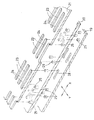
次に、フレキシブルフラットケーブル40の構成について、 図8(a)及び 図8(b)を参照しながら説明する。
フレキシブルフラットケーブル40は、トップシート35の上面に重ねられ、ノズル列と直交する方向(X方向)に外方へ突出して配置される( 図1参照)。フレキシブルフラットケーブル40は、帯状のベース材100と、その片面に形成された配線79及びコモン電極用の接合電極部77、個別電極用の接合電極部78と、これらの表面を被覆するカバーレイ101とで構成されている。ベース材100及びカバーレイ101は、電気絶縁性を有し、可撓性の合成樹脂材(例えば、ポリイミド樹脂、ポリエステル樹脂、ポリアミド樹脂)からなる。接合電極部77,7及び配線79はベース材100の片面に銅箔にてフォトレジスト法等により形成されている。配線79はベース材100に搭載された駆動用の集積回路102に電気的に接合されている。フレキシブルフラットケーブル40の外方へ突出した端部に設けられた複数の端子105は、集積回路102と接続されている。なお、島状の個別電極用の接合電極部78は、トップシート35上の接合端子91の外部電極95とそれぞれ対面する位置にあって、その対面する部位のベース材100に開けられた孔(開口部)の部位に半田合金からなるバンプ電極103を固着している( 図8(b)参照)。同様に、帯状のコモン電極用の接合電極部77(後述する77−1及び77−2)のうち、トップシート35上の接合端子90の外部電極94とそれぞれ対面する箇所に開けられた孔(開口部)の部位にバンプ電極103を固着している。
11 キャビティユニット
11a ノズル
12 圧電アクチュエータ
22 ベースプレート
23 圧力室
33,34 圧電シート
35 トップシート
36 個別電極
37 コモン電極
40 フラットケーブル
53 接続用パターン
54 連絡用パターン
77 コモン電極用の接合電極部
78 個別電極用の接合電極部
79 配線
90 コモン電極用接合端子
91 個別電極用接合端子
92、93 表面電極
94、95 外部電極
102 集積回路
103 バンプ電極
103a 隅肉部
Claims (11)
- 第1の方向に沿って列状に配置された複数個のノズルと、各ノズルに対応した圧力室と、前記各圧力室に対応しインクに選択的に噴出エネルギーを与える複数個のエネルギー発生手段を有するアクチュエータと、該アクチュエータの表面に前記各エネルギー発生手段に個別に対応して島状に配置された複数の接合端子に回路素子から所定電圧の波形信号を出力する配線基板とを備えるインクジェット記録ヘッドにおいて前記配線基板を前記接合端子に接続する接合構造であって、
前記配線基板は、溶融可能なバンプ電極を前記接合端子と重ね接合される位置に備え、
前記接合端子は、前記アクチュエータの表面に形成した表面電極と、該表面電極の表面上に突出して形成され、前記バンプ電極との接合性が前記表面電極よりも良い外部電極とからなり、
前記表面電極は、第1の方向に並んで配列されるとともに、その第1の方向と直交する第2の方向に前記外部電極よりも長く形成され、かつ一端に平面視において前記各外部電極を囲む周縁を有する広幅部を有するとともに、該広幅部から前記第2の方向に延び該広幅部よりも前記第1の方向の幅を狭くした細幅部を有し、
前記複数の表面電極は、該表面電極の前記広幅部と前記細幅部とが交互に逆向きに位置するように、前記第1の方向に配置されているとともに、前記外部電極は、前記各表面電極の広幅部上に配置され、
前記バンプ電極は、溶融した後固化した状態で、前記外部電極及び前記表面電極を覆っていることを特徴とするインクジェット記録ヘッドにおける配線基板の接合構造。 - 前記インクジェット記録ヘッドは、第1の方向に沿って列状に配置された複数個のノズルからなるノズルの列及びそれに対応する圧力室の列を、第2の方向に複数列備えるとともに、前記複数の圧力室の列に対応して、複数個のエネルギー発生手段を備え、前記アクチュエータの表面に、複数個のエネルギー発生手段に接続した前記表面電極を備え、
前記複数の表面電極は、各表面電極の列ごとに、該表面電極の前記広幅部と前記細幅部とが交互に逆向きに位置するように、前記第1の方向に配置されていることを特徴とする請求項1に記載のインクジェット記録ヘッドにおける配線基板の接合構造。 - 前記外部電極は、前記広幅部の表面に、該広幅部の周縁よりも内周側に該外部電極の周縁が位置するように配置され、
前記バンプ電極は、前記外部電極の上面及び側面を覆い、前記広幅部の表面を周縁近傍まで覆っていることを特徴とする請求項1または2に記載のインクジェット記録ヘッドにおける配線基板の接合構造。 - 前記表面電極及び前記外部電極は、前記各圧力室間を仕切る隔壁と対応して位置することを特徴とする請求項1ないし3のいずれかに記載のインクジェット記録ヘッドにおける配線基板の接合構造。
- 前記アクチュエータは、圧電シートを含む複数のシートを積層して焼成したものから構成され、該シートのうち最上層のシートの表面に前記表面電極が形成され、該表面電極の表面に前記外部電極が形成されていることを特徴とする請求項1ないし4のいずれかに記載のインクジェット記録ヘッドにおける配線基板の接合構造。
- 前記最上層のシートは、該シートを板厚方向に貫通しかつ上面において前記表面電極と接続した内部導通電極を有し、該内部導通電極の上面部位に対し、充填電極と、該充填電極を兼用する前記外部電極とを、前記表面電極の列方向に、交互に配置したことを特徴とする請求項5に記載のインクジェット記録ヘッドにおける配線基板の接合構造。
- 前記インクジェット記録ヘッドは、前記複数のエネルギー発生手段に共通に接続されたコモン電極用接合端子を備え、該コモン電極用接合端子は、前記アクチュエータの表面のうち外周縁寄り部位に帯状に形成された表面電極と、該表面電極の表面に形成された外部電極とからなり、前記配線基板は、該外部電極と対応するバンプ電極を備えることを特徴とする請求項1ないし6のいずれかに記載のインクジェット記録ヘッドにおける配線基板の接合構造。
- 前記表面電極は、銀−パラジュウム系導電材料であり、前記外部電極は、銀−ガラスフリット系導電材料であることを特徴とする請求項1ないし7のいずれかに記載のインクジェット記録ヘッドにおける配線基板の接合構造。
- 請求項1に記載のインクジェット記録ヘッドにおける配線基板の接合構造における、前記配線基板を、前記接合端子に接続する、前記配線基板の接合方法であって、
前記バンプ電極を前記外部電極に重ねて加熱押圧することで、該バンプ電極を溶融して、前記外部電極及び前記表面電極を覆った状態で固化させることを特徴とするインクジェット記録ヘッドにおける配線基板の接合方法。 - 前記アクチュエータは、圧電シートを含む積層した複数のシートを含み、
該シートの元材料であるグリーンシートの表面に、前記表面電極を印刷形成した後焼成し、該焼成した前記表面電極の表面に、前記外部電極を印刷形成した後、前記焼成温度よりも低い温度で焼成することを特徴とする請求項9に記載のインクジェット記録ヘッドにおける配線基板の接合方法。 - 前記表面電極に、銀−パラジュウム系導電材料を用い、前記外部電極に、銀−ガラスフリット系導電材料を用いることを特徴とする請求項9または10に記載のインクジェット記録ヘッドにおける配線基板の接合方法。
Priority Applications (3)
| Application Number | Priority Date | Filing Date | Title |
|---|---|---|---|
| JP2004015494A JP4161213B2 (ja) | 2004-01-23 | 2004-01-23 | インクジェット記録ヘッドにおける配線基板の接合構造及びその接合方法 |
| US11/040,744 US7416279B2 (en) | 2004-01-23 | 2005-01-21 | Connection structure for inkjet recording head |
| US11/171,929 US7517065B2 (en) | 2004-01-23 | 2005-06-29 | Injet printhead having externally-connected terminations structured to be resistant to damage |
Applications Claiming Priority (1)
| Application Number | Priority Date | Filing Date | Title |
|---|---|---|---|
| JP2004015494A JP4161213B2 (ja) | 2004-01-23 | 2004-01-23 | インクジェット記録ヘッドにおける配線基板の接合構造及びその接合方法 |
Publications (3)
| Publication Number | Publication Date |
|---|---|
| JP2005205769A JP2005205769A (ja) | 2005-08-04 |
| JP2005205769A5 JP2005205769A5 (ja) | 2008-07-17 |
| JP4161213B2 true JP4161213B2 (ja) | 2008-10-08 |
Family
ID=34792439
Family Applications (1)
| Application Number | Title | Priority Date | Filing Date |
|---|---|---|---|
| JP2004015494A Expired - Lifetime JP4161213B2 (ja) | 2004-01-23 | 2004-01-23 | インクジェット記録ヘッドにおける配線基板の接合構造及びその接合方法 |
Country Status (2)
| Country | Link |
|---|---|
| US (1) | US7416279B2 (ja) |
| JP (1) | JP4161213B2 (ja) |
Families Citing this family (17)
| Publication number | Priority date | Publication date | Assignee | Title |
|---|---|---|---|---|
| JP4507170B2 (ja) * | 2004-02-23 | 2010-07-21 | ブラザー工業株式会社 | インクジェットプリンタヘッド |
| US7525240B2 (en) | 2004-04-26 | 2009-04-28 | Tdk Corporation | Electronic component |
| JP4940672B2 (ja) * | 2006-01-27 | 2012-05-30 | ブラザー工業株式会社 | インクジェット式記録ヘッド |
| JP4934325B2 (ja) * | 2006-02-17 | 2012-05-16 | 株式会社フジクラ | プリント配線板の接続構造及びプリント配線板の接続方法 |
| JP5194386B2 (ja) * | 2006-06-03 | 2013-05-08 | ブラザー工業株式会社 | 積層型圧電アクチュエータ |
| US7497558B2 (en) * | 2006-06-03 | 2009-03-03 | Brother Kogyo Kabushiki Kaisha | Piezoelectric actuator and liquid-droplet jetting head |
| JP5194385B2 (ja) * | 2006-06-03 | 2013-05-08 | ブラザー工業株式会社 | 積層型圧電アクチュエータ及びその製造方法 |
| JP5526464B2 (ja) * | 2006-06-03 | 2014-06-18 | ブラザー工業株式会社 | 積層型圧電アクチュエータ |
| JP5034593B2 (ja) * | 2007-03-26 | 2012-09-26 | ブラザー工業株式会社 | 駆動回路付き配線基板の構造および液滴吐出ヘッド |
| JP5006680B2 (ja) * | 2007-03-30 | 2012-08-22 | キヤノン株式会社 | インクジェット記録ヘッドおよびインクジェット記録ヘッドの製造方法 |
| US8104860B2 (en) * | 2007-09-28 | 2012-01-31 | Brother Kogyo Kabushiki Kaisha | Ink-jet recording apparatus including abnormality judging portion |
| JP2009094120A (ja) * | 2007-10-04 | 2009-04-30 | Brother Ind Ltd | 圧電アクチュエータ、これを用いた液滴吐出ヘッド、及び圧電アクチュエータの製造方法 |
| CN101946405A (zh) * | 2008-02-18 | 2011-01-12 | 精工电子有限公司 | 压电振动器的制造方法、压电振动器、振荡器、电子设备及电波钟 |
| JP5157989B2 (ja) * | 2009-03-26 | 2013-03-06 | ブラザー工業株式会社 | 圧電アクチュエータとこれを用いた液滴吐出ヘッド |
| JP5126208B2 (ja) * | 2009-11-30 | 2013-01-23 | ブラザー工業株式会社 | 圧電アクチュエータ、液体吐出ヘッド、圧電アクチュエータの製造方法、及び液体吐出ヘッドの製造方法 |
| JP6942607B2 (ja) * | 2017-10-30 | 2021-09-29 | キヤノン株式会社 | 液体吐出ヘッド及びその製造方法 |
| JP7106938B2 (ja) * | 2018-03-30 | 2022-07-27 | ブラザー工業株式会社 | 液体吐出ヘッド |
Family Cites Families (25)
| Publication number | Priority date | Publication date | Assignee | Title |
|---|---|---|---|---|
| US5912684A (en) * | 1990-09-21 | 1999-06-15 | Seiko Epson Corporation | Inkjet recording apparatus |
| US5315472A (en) * | 1991-07-23 | 1994-05-24 | Hewlett Packard Company | Ground ring/spark gap ESD protection of tab circuits |
| EP0622240B1 (en) * | 1993-04-30 | 1998-06-10 | Hewlett-Packard Company | Modular carriage assembly for an ink jet printer |
| US6003974A (en) * | 1993-04-30 | 1999-12-21 | Hewlett-Packard Company | Unitary interconnect system for an inkjet printer |
| EP0629502B1 (en) * | 1993-06-16 | 1998-09-02 | Seiko Epson Corporation | Inkjet recording apparatus |
| US5818473A (en) * | 1993-07-14 | 1998-10-06 | Seiko Epson Corporation | Drive method for an electrostatic ink jet head for eliminating residual charge in the diaphragm |
| US5644341A (en) * | 1993-07-14 | 1997-07-01 | Seiko Epson Corporation | Ink jet head drive apparatus and drive method, and a printer using these |
| JPH09109394A (ja) * | 1995-10-18 | 1997-04-28 | Canon Inc | 記録ヘッド |
| US6062675A (en) * | 1996-01-09 | 2000-05-16 | Canon Kabushiki Kaisha | Recording head, recording apparatus and manufacturing method of recording head |
| JPH10211701A (ja) * | 1996-11-06 | 1998-08-11 | Seiko Epson Corp | 圧電体素子を備えたアクチュエータ及びインクジェット式記録ヘッド、並びにこれらの製造方法 |
| JPH10217461A (ja) * | 1997-02-06 | 1998-08-18 | Minolta Co Ltd | インクジェット記録装置 |
| JPH11320873A (ja) * | 1997-06-05 | 1999-11-24 | Ricoh Co Ltd | インクジェットヘッド |
| JPH11147311A (ja) | 1997-11-17 | 1999-06-02 | Fujitsu Ltd | インクジェット記録ヘッド |
| US6454394B2 (en) * | 2000-03-21 | 2002-09-24 | Olympus Optical Co., Ltd. | Inkjet head which prevents transfer of a load applied to an inkjet-head-side connector |
| JP2002103691A (ja) * | 2000-10-05 | 2002-04-09 | Fuji Photo Film Co Ltd | 階調再現方法および階調再現画像 |
| JP2003165212A (ja) * | 2001-11-30 | 2003-06-10 | Brother Ind Ltd | インクジェットヘッド |
| US6595628B2 (en) * | 2001-02-19 | 2003-07-22 | Brother Kogyo Kabushiki Kaisha | Laminated piezoelectric element for use as a drive device |
| JP3767395B2 (ja) | 2001-03-01 | 2006-04-19 | ブラザー工業株式会社 | 積層型圧電素子の製造方法 |
| US7149090B2 (en) * | 2001-09-11 | 2006-12-12 | Brother Kogyo Kabushiki Kaisha | Structure of flexible printed circuit board |
| JP2003159795A (ja) | 2001-09-11 | 2003-06-03 | Brother Ind Ltd | 記録装置 |
| US6619787B2 (en) * | 2001-10-31 | 2003-09-16 | Hewlett-Packard Development Company, L.P. | Limiting unwanted ink penetration of flexible circuits of fluid ejection devices |
| JP4296738B2 (ja) * | 2001-11-30 | 2009-07-15 | ブラザー工業株式会社 | インクジェットヘッド |
| JP3861673B2 (ja) * | 2001-11-30 | 2006-12-20 | ブラザー工業株式会社 | インクジェット記録ヘッド |
| US6971738B2 (en) * | 2001-12-06 | 2005-12-06 | Brother Kogyo Kabushiki Kaisha | Piezoelectric actuator |
| JP3922151B2 (ja) * | 2002-09-27 | 2007-05-30 | ブラザー工業株式会社 | フレキシブル配線基板の接続構造および接続方法 |
-
2004
- 2004-01-23 JP JP2004015494A patent/JP4161213B2/ja not_active Expired - Lifetime
-
2005
- 2005-01-21 US US11/040,744 patent/US7416279B2/en active Active
Also Published As
| Publication number | Publication date |
|---|---|
| US7416279B2 (en) | 2008-08-26 |
| JP2005205769A (ja) | 2005-08-04 |
| US20050162484A1 (en) | 2005-07-28 |
Similar Documents
| Publication | Publication Date | Title |
|---|---|---|
| US7416279B2 (en) | Connection structure for inkjet recording head | |
| US7517065B2 (en) | Injet printhead having externally-connected terminations structured to be resistant to damage | |
| US7294952B2 (en) | Laminated-type piezoelectric element and inkjet recording head having the same | |
| JP2005205769A5 (ja) | ||
| US7900355B2 (en) | Ink-jet head and method for manufacturing the same | |
| JP4419754B2 (ja) | インクジェットヘッド | |
| US7469994B2 (en) | Ink-jet head and connecting structure | |
| JP4940672B2 (ja) | インクジェット式記録ヘッド | |
| JP5211631B2 (ja) | 液滴吐出装置及びその製造方法 | |
| JP4379583B2 (ja) | インクジェット記録ヘッド | |
| JP4552671B2 (ja) | 基板接合体、インクジェットヘッド及びこれらの製造方法 | |
| JP2007203481A (ja) | インクジェット式記録ヘッド | |
| JP2007203482A (ja) | インクジェットプリンタヘッド及びヘッドユニット | |
| JP4882083B2 (ja) | インクジェットヘッドの組み立て方法 | |
| US8083331B2 (en) | Piezoelectric actuator, liquid ejection head, and method for manufacturing piezoelectric actuator | |
| JP2006231913A (ja) | インクジェットヘッド、及び、フレキシブル配線基板と端子形成部材との接続構造 | |
| JP4221596B2 (ja) | インクジェット記録ヘッドにおけるフレキシブルフラットケーブルの接合構造 | |
| JP5526464B2 (ja) | 積層型圧電アクチュエータ | |
| JP5157989B2 (ja) | 圧電アクチュエータとこれを用いた液滴吐出ヘッド | |
| JP2006015539A5 (ja) | ||
| JP3885696B2 (ja) | インクジェットヘッド | |
| JP2005280044A (ja) | インクジェットヘッドの製造方法 | |
| JP5194385B2 (ja) | 積層型圧電アクチュエータ及びその製造方法 | |
| JP5194386B2 (ja) | 積層型圧電アクチュエータ | |
| JP2010260188A (ja) | 液滴吐出ヘッド |
Legal Events
| Date | Code | Title | Description |
|---|---|---|---|
| A621 | Written request for application examination |
Free format text: JAPANESE INTERMEDIATE CODE: A621 Effective date: 20061227 |
|
| A521 | Request for written amendment filed |
Free format text: JAPANESE INTERMEDIATE CODE: A523 Effective date: 20080530 |
|
| TRDD | Decision of grant or rejection written | ||
| A01 | Written decision to grant a patent or to grant a registration (utility model) |
Free format text: JAPANESE INTERMEDIATE CODE: A01 Effective date: 20080625 |
|
| A01 | Written decision to grant a patent or to grant a registration (utility model) |
Free format text: JAPANESE INTERMEDIATE CODE: A01 |
|
| A61 | First payment of annual fees (during grant procedure) |
Free format text: JAPANESE INTERMEDIATE CODE: A61 Effective date: 20080708 |
|
| FPAY | Renewal fee payment (event date is renewal date of database) |
Free format text: PAYMENT UNTIL: 20110801 Year of fee payment: 3 |
|
| R150 | Certificate of patent or registration of utility model |
Free format text: JAPANESE INTERMEDIATE CODE: R150 Ref document number: 4161213 Country of ref document: JP Free format text: JAPANESE INTERMEDIATE CODE: R150 |
|
| FPAY | Renewal fee payment (event date is renewal date of database) |
Free format text: PAYMENT UNTIL: 20120801 Year of fee payment: 4 |
|
| FPAY | Renewal fee payment (event date is renewal date of database) |
Free format text: PAYMENT UNTIL: 20120801 Year of fee payment: 4 |
|
| FPAY | Renewal fee payment (event date is renewal date of database) |
Free format text: PAYMENT UNTIL: 20130801 Year of fee payment: 5 |
|
| EXPY | Cancellation because of completion of term |