JP4156136B2 - Method for manufacturing buried optical waveguide - Google Patents
Method for manufacturing buried optical waveguide Download PDFInfo
- Publication number
- JP4156136B2 JP4156136B2 JP19819499A JP19819499A JP4156136B2 JP 4156136 B2 JP4156136 B2 JP 4156136B2 JP 19819499 A JP19819499 A JP 19819499A JP 19819499 A JP19819499 A JP 19819499A JP 4156136 B2 JP4156136 B2 JP 4156136B2
- Authority
- JP
- Japan
- Prior art keywords
- ion
- ion exchange
- refractive index
- substrate
- optical waveguide
- Prior art date
- Legal status (The legal status is an assumption and is not a legal conclusion. Google has not performed a legal analysis and makes no representation as to the accuracy of the status listed.)
- Expired - Fee Related
Links
Images


Landscapes
- Optical Integrated Circuits (AREA)
Description
【0001】
【発明の属する技術分野】
本発明は、2段階イオン交換法による低損失の埋め込み型光導波路の製造方法に関し、更に詳しく述べると、ガラス基板中に十分な深さまで埋め込まれた屈折率増加部分の断面イオン濃度分布形状を、基板深さ方向でほぼ対称形にする方法に関するものである。
【0002】
【従来の技術】
各種の光通信用伝送素子、光集積回路、あるいは光センサ用素子などでは、ガラス状物質からなる基板中に光導波路を形成する技術が必要となる。従来、この種の光導波路の形成には、イオン交換法が採用されている。このイオン交換法による光導波路の形成においては、基板表面の散乱による伝播損失を低減するために、また光ファイバとのモードフィールド整合のために、基板内部に光導波路を埋め込む2段階イオン交換法が一般的である。
【0003】
2段階イオン交換法は、熱イオン交換により屈折率増加部分を形成する第1のイオン交換工程と、電界印加により該屈折率増加部分を基板深さ方向に埋め込む第2のイオン交換工程を組み合わせた方法である。第1のイオン交換工程では、アルカリイオンを含むガラス基板上に、所定の光導波路パターンを有するイオン交換制御膜を形成し、AgあるいはTl等の屈折率を増加させる1価イオンを含む硝酸塩や硫酸塩の溶融塩に適当な時間浸漬して、前記イオン交換制御膜を通して熱イオン交換を行い屈折率増加部分を形成する。この第1のイオン交換工程の後、前記イオン交換制御膜をエッチングにより除去する。次いで、第2のイオン交換工程では、ガラス基板をNa又はKイオンを含む溶融塩中に浸漬し、電界を印加しながらイオン交換し、AgあるいはTlイオンによる屈折率増加部分をガラス基板の深さ方向に埋め込む。
【0004】
このようにして形成された屈折率増加部分が光導波路として機能する。光導波路を基板表面近傍に形成した場合、基板表面の表面あれや基板表面上の材料などにより、導波光の散乱や吸収が発生する。これは、導波光のエネルギのしみだしが基板表面上までも起こっているためである。この影響を回避するために、上記のように、光導波路を基板内部に埋め込むことが行われているのである。
【0005】
【発明が解決しようとする課題】
一般に、埋め込み深さが大きくなればなるほど、それだけ基板表面の影響を受け難くなり、低損失の光導波路が実現できる。必要な埋め込み深さは、使用波長や光導波路の設計などにより異なるが、通信波長域の用途を考慮すると10μm程度が目安となる。しかし、埋め込み深さが大きくなるほど、屈折率増加部分の断面イオン濃度分布形状がいびつになり、真円からはほど遠いものとなる。ここで、「埋め込み深さ」とは、屈折率増加部分中で屈折率を増加させるイオンの濃度が最も大きい点の基板表面からの深さをいう。
【0006】
ところで、AgやTl等の屈折率を増加させる1価イオンのガラス中における拡散係数や移動度には、多かれ少なかれ濃度依存性が存在する。具体的には、ガラス中のイオン濃度が高い部分は拡散係数や移動度が大きく、イオン濃度が低い部分は拡散係数や移動度が小さくなる。従って、電界印加による第2のイオン交換では、その依存性の影響で、埋め込み深さが大きくなるほど、屈折率増加部分が基板深さ方向で上下非対称となることは避けられず、モードフィールド自体も当然非対称になってしまう。このような理由で、屈折率増加部分の断面イオン濃度分布が真円で、且つシングルモードとなる光導波路の実現は非常に困難であった。そのため、光ファイバとの整合性に劣り、光ファイバと結合する際の損失が大きくなる欠点があった。
【0007】
本発明の目的は、2段階イオン交換法を用いて、埋め込み深さを大きくするにもかかわらず、光ファイバとの整合性の良い軸対称形の屈折率増加部分を形成できるようにした埋め込み型光導波路の製造方法を提供することである。
【0008】
【課題を解決するための手段】
本発明は、1価のイオンを含有してイオン交換可能なガラス状物質からなる基板上に、所定の光導波路パターンを有するイオン交換制御膜を形成し、前記基板の屈折率を増加させ得る第1の1価イオンを含有する第1の溶融塩に浸漬して、前記イオン交換制御膜を通して熱イオン交換を行い屈折率増加部分を形成する第1のイオン交換工程と、前記基板から前記イオン交換制御膜を除去するエッチング工程と、エッチング処理した基板を、前記第1のイオン交換工程によって屈折率が増加した部分の屈折率を下げ得る第2の1価イオンを含有する第2の溶融塩に浸漬しながら、前記イオン交換制御膜の形成されていた側を正電位とし、反対側を負電位として基板にほぼ垂直に電界を印加して前記第1の1価イオンによる屈折率増加部分を前記基板の深さ方向に埋め込む第2のイオン交換工程とを、この順で行う埋め込み型光導波路の製造方法を前提とするものである。
【0009】
本発明の第1の方法は、前記第2のイオン交換工程における印加電界強度を、時間と共に低下させて、埋め込まれる第1の1価イオンによる屈折率増加部分の断面イオン濃度分布形状を、ほぼ軸対称形に整形しつつ埋め込む方法である。第2のイオン交換の際に、時間に依らず一定強度の電界を印加すると、イオン移動度の濃度依存性から高イオン濃度領域が深く、低濃度領域が浅く埋め込まれ、イオン濃度分布が非対称形状となっていた。それに対して上記のように、第2のイオン交換工程で、時間と共に印加電界強度を低下させることにより、電界によるイオン移動度に対する熱によるイオン拡散の影響を大きくすることができ、屈折率増加部分のイオン濃度分布の断面形状の非対称性を低減できる。
【0010】
本発明の第2の方法は、前記第2のイオン交換工程後に、前記基板を第2の溶融塩に浸漬しながら、第2のイオン交換工程とは逆向きの電界を印加する第3のイオン交換工程を具備し、第2のイオン交換工程によって埋め込まれた第1の1価イオンによる屈折率増加部分のイオン濃度分布の断面形状を、前記第3のイオン交換工程によってほぼ軸対称形に整形する方法である。逆電界を印加する第3のイオン交換工程によって、屈折率増加部分の特に高イオン濃度領域のみを選択的に移動させ、屈折率増加イオン濃度の断面分布形状の非対称性を低減できる。ここで逆電界を印加する第3のイオン交換工程は、交換イオンの熱による移動度を極力抑制し、電界による高イオン濃度領域の移動度をより大きくする。
【0011】
本発明の第3の方法は、前記第2のイオン交換工程後に、基板を無電界状態で加熱保持する熱処理工程を具備し、第2のイオン交換工程によって埋め込まれた第1の1価イオンによる屈折率増加部分のイオン濃度分布の断面形状を、前記熱処理工程によってほぼ軸対称形に整形する方法である。第2のイオン交換工程後の熱処理により、空間的なイオン濃度勾配の大きな部分が選択的に拡散する。また、拡散定数の濃度依存性からもイオン濃度の高い部分の選択的拡散が実現される。更に、一旦拡散により移動し低濃度化した部分は、拡散定数の濃度依存性から考えて時間的に形状変化の少ない定常状態を実現して安定化する作用をもつ。この熱処理は、第2のイオン交換を行った後の基板を、第2のイオン交換工程で用いる第2の溶融塩に一定時間浸漬することで簡便に実施できる。
【0012】
【発明の実施の形態】
本発明は、特に埋め込み深さが10μm以上の光導波路に有効である。従来の2段階イオン交換法では、埋め込み深さが大きくなればなるほど屈折率増加部分のイオン濃度分布の断面形状の非対称性が甚だしくなり、それを改善する必要性も大きくなるからである。前記第1の方法における印加電界強度の変化パターンと時間、第2の方法における印加逆電界強度と時間、第3の方法における温度と時間などは、いずれも基板材質や使用するイオンの種類、光導波路の設計値等に応じて適宜決定すればよい。
【0013】
基板の屈折率を増加させ得る第1の1価イオンとしては、Agイオン、Tlイオン、Csイオン、Rbイオン、Kイオン、Liイオンのうちの少なくとも1種のイオンを用いる。また、第1の1価イオンにより形成された屈折率増加部分の屈折率を下げ得る第2の1価イオンとしては、Naイオン又はKイオンの少なくとも1種のイオンを用いる。
【0014】
ガラス状物質の基板としては、例えばアルミノボロシリケート系ガラス、アルミノシリケート系ガラス、ボロシリケート系ガラスのいずれかを用いる。
【0015】
【実施例】
(実施例1−1)
アルカリイオンとしてNaイオンのみが含まれるアルミノボロシリケート系ガラス基板上に、所定の光導波路パターンの開口を有するTiのイオン交換制御膜を形成し、AgNO3 とNaNO3 よりなる溶融塩(AgNO3 濃度10%)中に、255℃で90分間浸漬する第1のイオン交換を行い、基板表面に屈折率増加部分を形成する。続いて、基板表面のイオン交換制御膜をエッチングにより除去する。その後、NaNO3 溶融塩中で、電界を印加した第2のイオン交換を行い、基板表面に形成された屈折率増加部分を基板内部に埋め込む。
【0016】
この第2のイオン交換工程は、印加する電界強度を時間的に次のようなパターンで変化させて行った。
(a)パターン:溶融塩温度255℃で、150V/mmの電界強度から直線的に180分かけて0V/mmに低下させながら行う。
(b)パターン:溶融塩温度255℃で、150V/mmの電界強度から直線的に180分かけて半値である75V/mmに低下させながら行う。
(c)パターン:比較のために、溶融塩温度255℃で、180分間、150V/mmの電界強度を一定に保って行う(従来技術)。
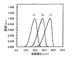
【0017】
この条件で作製した3.5μmの光導波路の屈折率増加イオンの濃度プロファイルをシミュレートした結果を、図1に示す。図1中、符号(a),…,(c)は、それぞれ上記の各パターンに対応したイオン濃度分布を示している。この結果より、第2のイオン交換工程で印加電界強度を低下させる本発明により、埋め込み深さが10μm以上となるように十分大きく、深さ方向に関してより対称性の良好なイオン濃度分布をもつように光導波路を整形できることが分かる。
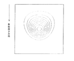
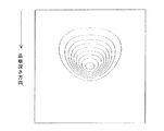
【0018】
図2と図3に屈折率増加イオンの断面濃度プロファイルを示す。図2は本発明方法(上記実施例1−1の(a)パターン)の場合であり、図3は従来技術(上記実施例1−1の(c)パターン:比較例)の場合である。図3(従来技術)では上下方向(深さ方向)で非対称の度合いが甚だしく、中央部も潰れて楕円状となっているが、図2(本発明方法)では、それが大きく改善され軸対称性が良好となり、特に中央部ではほぼ真円となっている。
【0019】
(実施例1−2)
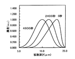
実施例1−1と同様の手順で屈折率増加部分を基板内部に埋め込む。第2のイオン交換工程は、処理時間のみ変えて、次のように電界強度を時間的に変化させて行った。
(d)パターン:溶融塩温度255℃で、150V/mmの電界強度から直線的に120分かけて0V/mmに低下させながら行う。
(e)パターン:溶融塩温度255℃で、150V/mmの電界強度から直線的に120分かけて半値である75V/mmに低下させながら行う。
(f)パターン:比較のために、溶融塩温度255℃で、120分間、150V/mmの電界強度を一定に保って行う(従来技術)。
【0020】
この条件で作製した3.5μmの光導波路の屈折率増加イオンの濃度プロファイルをシミュレートした結果を、図4に示す。図4中、符号(d),…,(f)は、それぞれ上記の各パターンに対応したイオン濃度分布を示している。この結果より、第2のイオン交換工程で印加電界強度を低下させる本発明により、埋め込み深さが10μm以上となるように十分大きく、深さ方向に関してより対称性の良好なイオン濃度分布をもつように光導波路を整形できることが分かる。
【0021】
(実施例2−1)
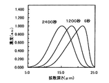
アルカリイオンとしてNaイオンのみが含まれるアルミノボロシリケート系ガラス基板上に、所定の光導波路パターンの開口を有するTiのイオン交換制御膜を形成し、AgNO3 とNaNO3 よりなる溶融塩(AgNO3 濃度10%)中に、255℃で90分間浸漬する第1のイオン交換を行い、基板表面に屈折率増加部分を形成する。続いて、基板表面のイオン交換制御膜をエッチングにより除去する。その後、NaNO3 溶融塩中で電界を印加した第2のイオン交換を、255℃、120V/mmの電界強度の下で120分間行い、基板表面に形成された屈折率増加部分を基板内部に埋め込む。
【0022】
更に、第2のイオン交換工程と同一温度、同一溶融塩中で、第2のイオン交換とは逆方向で、より高い150V/mmの電界下で最長20分間までの第3のイオン交換を行った。
【0023】
この条件で作製した3.5μmの光導波路の屈折率増加イオンの濃度プロファイルをシミュレートした結果を図5に示す。図5において、各曲線は処理時間を示している。未処理は、第2のイオン交換終了時点のデータであり、従来技術に相当する。この結果より、第3のイオン交換工程で逆方向の電界強度を印加する本発明により、埋め込み深さが10μm以上となるように十分大きく、深さ方向に関してより対称性の良好なイオン濃度分布をもつように屈折率増加部分を整形できることが分かる。
【0024】
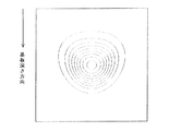
また図6に本発明方法(上記実施例2−1)の場合の屈折率増加イオンの断面濃度プロファイルを示す。図3の従来技術と比べれば明瞭なように、図6(本発明方法)では、上下方向(深さ方向)で非対称の度合いが大きく改善され、特に中央部ではほぼ真円になることが分かる。
【0025】
(実施例2−2)
実施例2−1と同様の手順で屈折率増加部分を基板内部に埋め込んだ。第3のイオン交換工程は、電界強度と処理時間を変えて行った。即ち、第2のイオン交換と同一温度、同一溶融塩中で、第2のイオン交換とは逆方向の100V/mmの電界下で40分間の第3のイオン交換を行った。この条件で作製した3.5μmの光導波路の屈折率増加イオンの濃度プロファイルをシミュレートした結果を図7に示す。
【0026】
(実施例2−3)
実施例2−1と同様の手順で屈折率増加部分を基板内部に埋め込んだ。第3のイオン交換工程は、電界強度と処理時間を変えて行った。即ち、第2のイオン交換と同一温度、同一溶融塩中で、第2のイオン交換とは逆方向の50V/mmの電界下で80分間の第3のイオン交換を行った。この条件で作製した3.5μmの光導波路の屈折率増加イオンの濃度プロファイルをシミュレートした結果を図8に示す。
【0027】
これらの結果からも、第3のイオン交換工程で逆向きの電界を印加する本発明により、埋め込み深さが10μm以上となるように十分大きく、深さ方向に関してより対称なイオン濃度分布をもつように光導波路を整形できることが分かる。
【0028】
(実施例3)
アルカリイオンとしてNaイオンのみが含まれるアルミノボロシリケート系ガラス基板上に、所定の光導波路パターンの開口を有するTiのイオン交換制御膜を形成し、AgNO3 とNaNO3 よりなる溶融塩(AgNO3 濃度5%)中に、280℃で120分間浸漬する第1のイオン交換を行い、基板表面に屈折率増加部分を形成する。続いて、基板表面のイオン交換制御膜をエッチングにより除去する。その後、NaNO3 溶融塩中で電界を印加した第2のイオン交換を、280℃、150V/mmの電界強度の下で120分間行い、基板表面に形成された屈折率増加部分を基板内部に埋め込む。更に、第2のイオン交換と同一温度、同一溶融塩中で、120分間の熱処理を行った。
【0029】
この条件で作製した3.5μmの光導波路の屈折率増加イオンの濃度プロファイルをBSE(back scattered electron )により分析した結果を図9に示す。また図10に本発明方法(上記実施例3)の場合の屈折率増加イオンの断面濃度プロファイルを示す。これらの結果から、第2のイオン交換工程後に熱処理を行う本発明により、埋め込み深さが10μm以上となるように十分大きく、深さ方向に関してより対称性の良好な屈折率分布をもつ光導波路に整形できることが分かる。また、図3の従来技術と比べれば明瞭なように、図10(本発明方法)では、上下方向(深さ方向)で非対称の度合いが大きく改善され、特に中央部ではほぼ真円になっていることが分かる。
【0030】
なお、上記の例では、熱処理工程を第2のイオン交換に用いたのと同じ溶融塩中に浸漬しながら行っているが、該溶融塩から取り出して別の雰囲気中での熱処理プロセスで行ってもよい。
【0031】
【発明の効果】
本発明は上記のように、原理的には2段階イオン交換法を用いる埋め込み型光導波路の製造方法を利用し、その第2のイオン交換工程、あるいは第2のイオン交換工程後の処理を工夫したことにより、屈折率増加部分を十分な深さに埋め込むことができ、そのため低損失であり、しかもその屈折率増加部分を軸対称性が良好となるように整形でき、そのため光ファイバとの整合性を改善できる。
【図面の簡単な説明】
【図1】実施例1−1における光導波路の屈折率増加イオンの濃度プロファイル。
【図2】本発明方法による光導波路の屈折率増加イオンの断面濃度プロファイル。
【図3】従来技術による光導波路の屈折率増加イオンの断面濃度プロファイル。
【図4】実施例1−2における光導波路の屈折率増加イオンの濃度プロファイル。
【図5】実施例2−1における光導波路の屈折率増加イオンの濃度プロファイル。
【図6】本発明方法による光導波路の屈折率増加イオンの断面濃度プロファイル。
【図7】実施例2−2における光導波路の屈折率増加イオンの濃度プロファイル。
【図8】実施例2−3における光導波路の屈折率増加イオンの濃度プロファイル。
【図9】実施例3における光導波路の屈折率増加イオンの濃度プロファイル。
【図10】本発明方法による光導波路の屈折率増加イオンの断面濃度プロファイル。[0001]
BACKGROUND OF THE INVENTION
The present invention relates to a method for producing a low-loss buried optical waveguide by a two-stage ion exchange method, and more specifically, the cross-sectional ion concentration distribution shape of the refractive index increasing portion buried to a sufficient depth in a glass substrate, The present invention relates to a method of making a substantially symmetrical shape in the substrate depth direction.
[0002]
[Prior art]
Various optical communication transmission elements, optical integrated circuits, or optical sensor elements require a technique for forming an optical waveguide in a substrate made of a glassy substance. Conventionally, an ion exchange method has been employed to form this type of optical waveguide. In the formation of the optical waveguide by this ion exchange method, there is a two-stage ion exchange method in which the optical waveguide is embedded in the substrate in order to reduce propagation loss due to scattering on the substrate surface and for mode field matching with the optical fiber. It is common.
[0003]
The two-stage ion exchange method combines a first ion exchange step for forming a refractive index increasing portion by thermal ion exchange and a second ion exchange step for embedding the refractive index increasing portion in the substrate depth direction by applying an electric field. Is the method. In the first ion exchange step, an ion exchange control film having a predetermined optical waveguide pattern is formed on a glass substrate containing alkali ions, and nitrate or sulfuric acid containing monovalent ions for increasing the refractive index such as Ag or Tl. It is immersed in a molten salt salt for an appropriate time, and thermal ion exchange is performed through the ion exchange control film to form a refractive index increasing portion. After the first ion exchange step, the ion exchange control film is removed by etching. Next, in the second ion exchange step, the glass substrate is immersed in a molten salt containing Na or K ions, ion exchange is performed while an electric field is applied, and the portion where the refractive index is increased by Ag or Tl ions is reduced to the depth of the glass substrate. Embed in the direction.
[0004]
The refractive index increasing portion formed in this way functions as an optical waveguide. When the optical waveguide is formed in the vicinity of the substrate surface, scattering or absorption of the guided light occurs due to surface roughness of the substrate surface or materials on the substrate surface. This is because the oozing of the energy of the guided light has occurred even on the substrate surface. In order to avoid this influence, the optical waveguide is embedded in the substrate as described above.
[0005]
[Problems to be solved by the invention]
In general, the greater the embedding depth, the less affected by the substrate surface, and a low-loss optical waveguide can be realized. The required embedding depth varies depending on the wavelength used, the design of the optical waveguide, and the like, but approximately 10 μm is a guide when considering the application in the communication wavelength region. However, as the embedding depth increases, the cross-sectional ion concentration distribution shape of the refractive index increasing portion becomes distorted and becomes far from the perfect circle. Here, the “embedding depth” refers to the depth from the substrate surface at the point where the concentration of ions that increase the refractive index is highest in the refractive index increasing portion.
[0006]
By the way, the diffusion coefficient and mobility of monovalent ions that increase the refractive index of Ag, Tl, etc. in the glass are more or less concentration dependent. Specifically, a portion having a high ion concentration in the glass has a large diffusion coefficient and mobility, and a portion having a low ion concentration has a small diffusion coefficient and mobility. Therefore, in the second ion exchange by applying an electric field, due to the dependency, it is inevitable that as the embedding depth increases, the refractive index increasing portion becomes vertically asymmetric in the substrate depth direction. Naturally it becomes asymmetric. For this reason, it has been very difficult to realize an optical waveguide in which the cross-sectional ion concentration distribution in the refractive index increasing portion is a perfect circle and is single mode. For this reason, there is a drawback in that the matching with the optical fiber is inferior and the loss in coupling with the optical fiber is increased.
[0007]
An object of the present invention is to provide a buried type in which an axially symmetric refractive index increasing portion having good matching with an optical fiber can be formed using a two-stage ion exchange method, even though the buried depth is increased. It is to provide a method for manufacturing an optical waveguide.
[0008]
[Means for Solving the Problems]
In the present invention, an ion exchange control film having a predetermined optical waveguide pattern is formed on a substrate made of a glassy substance containing monovalent ions and capable of ion exchange, and the refractive index of the substrate can be increased. A first ion exchange step of immersing in a first molten salt containing one monovalent ion and performing a thermal ion exchange through the ion exchange control film to form a refractive index increasing portion; and the ion exchange from the substrate. The etching step for removing the control film and the etched substrate into the second molten salt containing the second monovalent ion capable of lowering the refractive index of the portion where the refractive index has been increased by the first ion exchange step. While dipping, the side where the ion exchange control film was formed was set to a positive potential, and the opposite side was set to a negative potential, and an electric field was applied almost perpendicularly to the substrate to increase the refractive index increase portion due to the first monovalent ions. A second ion exchange step of embedding in the depth direction of the plate, is to assume a method of manufacturing an embedded type optical waveguide performed in this order.
[0009]
In the first method of the present invention, the applied electric field strength in the second ion exchange step is decreased with time, and the cross-sectional ion concentration distribution shape of the refractive index increasing portion due to the embedded first monovalent ions is approximately This is a method of embedding while shaping into an axially symmetric shape. In the second ion exchange, if an electric field having a constant intensity is applied regardless of time, the high concentration region is deep and the low concentration region is embedded shallowly due to the concentration dependence of ion mobility, and the ion concentration distribution is asymmetrical. It was. On the other hand, as described above, in the second ion exchange step, the influence of ion diffusion due to heat on the ion mobility due to the electric field can be increased by decreasing the applied electric field strength with time, and the refractive index increasing portion. Asymmetry of the cross-sectional shape of the ion concentration distribution can be reduced.
[0010]
In the second method of the present invention, after the second ion exchange step, a third ion that applies an electric field opposite to that in the second ion exchange step while immersing the substrate in a second molten salt. A cross-sectional shape of the ion concentration distribution of the refractive index increasing portion due to the first monovalent ions embedded by the second ion exchange step is formed into a substantially axisymmetric shape by the third ion exchange step. It is a method to do. By the third ion exchange process in which a reverse electric field is applied, only the high ion concentration region of the refractive index increasing portion can be selectively moved, and the asymmetry of the cross-sectional distribution shape of the refractive index increasing ion concentration can be reduced. Here, in the third ion exchange step of applying the reverse electric field, the mobility of exchange ions due to heat is suppressed as much as possible, and the mobility of the high ion concentration region due to the electric field is further increased.
[0011]
The third method of the present invention includes a heat treatment step for heating and holding the substrate in an electric field-free state after the second ion exchange step, and the first monovalent ions embedded by the second ion exchange step. In this method, the cross-sectional shape of the ion concentration distribution in the refractive index increasing portion is shaped into a substantially axisymmetric shape by the heat treatment step. Due to the heat treatment after the second ion exchange step, a portion having a large spatial ion concentration gradient is selectively diffused. Further, selective diffusion of a portion having a high ion concentration is realized from the concentration dependency of the diffusion constant. Further, the portion once moved by diffusion and reduced in concentration has the effect of stabilizing by realizing a steady state with little shape change in time considering the concentration dependency of the diffusion constant. This heat treatment can be easily carried out by immersing the substrate after the second ion exchange in the second molten salt used in the second ion exchange step for a certain period of time.
[0012]
DETAILED DESCRIPTION OF THE INVENTION
The present invention is particularly effective for an optical waveguide having a buried depth of 10 μm or more. This is because, in the conventional two-stage ion exchange method, as the embedding depth increases, the asymmetry of the cross-sectional shape of the ion concentration distribution in the refractive index increasing portion increases, and the need to improve it increases. The change pattern and time of the applied electric field strength in the first method, the applied reverse electric field strength and time in the second method, the temperature and time in the third method, etc. are all the substrate material, the type of ions used, the light What is necessary is just to determine suitably according to the design value etc. of a waveguide.
[0013]
As the first monovalent ions that can increase the refractive index of the substrate, at least one ion of Ag ions, Tl ions, Cs ions, Rb ions, K ions, and Li ions is used. In addition, as the second monovalent ion that can lower the refractive index of the refractive index increasing portion formed by the first monovalent ion, at least one kind of ion of Na ion or K ion is used.
[0014]
As the substrate of the glassy substance, for example, any of aluminoborosilicate glass, aluminosilicate glass, and borosilicate glass is used.
[0015]
【Example】
(Example 1-1)
A Ti ion exchange control film having an opening of a predetermined optical waveguide pattern is formed on an aluminoborosilicate glass substrate containing only Na ions as alkali ions, and a molten salt (AgNO 3 concentration) made of AgNO 3 and NaNO 3 is formed. 10%), the first ion exchange is performed for 90 minutes at 255 ° C. to form a refractive index increasing portion on the substrate surface. Subsequently, the ion exchange control film on the substrate surface is removed by etching. Thereafter, in the NaNO 3 molten salt, second ion exchange is performed by applying an electric field, and the refractive index increasing portion formed on the substrate surface is embedded inside the substrate.
[0016]
This second ion exchange step was performed by changing the applied electric field intensity temporally in the following pattern.
(A) Pattern: Performed at a molten salt temperature of 255 ° C. while linearly decreasing from an electric field strength of 150 V / mm to 0 V / mm over 180 minutes.
(B) Pattern: At a molten salt temperature of 255 ° C., the electric field strength is 150 V / mm, linearly lowered to 75 V / mm, which is a half value over 180 minutes.
(C) Pattern: For comparison, an electric field strength of 150 V / mm is kept constant for 180 minutes at a molten salt temperature of 255 ° C. (prior art).
[0017]
FIG. 1 shows the result of simulating the concentration profile of the refractive index increasing ion of the 3.5 μm optical waveguide manufactured under these conditions. In FIG. 1, symbols (a),..., (C) indicate ion concentration distributions corresponding to the respective patterns. As a result, the present invention that reduces the applied electric field strength in the second ion exchange step is sufficiently large so that the embedding depth is 10 μm or more, and has an ion concentration distribution with better symmetry in the depth direction. It can be seen that the optical waveguide can be shaped.
[0018]
2 and 3 show cross-sectional concentration profiles of ions with increased refractive index. FIG. 2 shows the case of the method of the present invention (the pattern (a) in Example 1-1), and FIG. 3 shows the case of the prior art (the pattern (c) in Example 1-1: comparative example). In FIG. 3 (prior art), the degree of asymmetry is significant in the vertical direction (depth direction), and the central part is also crushed into an elliptical shape. However, in FIG. In particular, the center portion is almost a perfect circle.
[0019]
(Example 1-2)
The refractive index increasing portion is embedded in the substrate in the same procedure as in Example 1-1. The second ion exchange step was performed by changing only the treatment time and changing the electric field intensity with time.
(D) Pattern: Performed at a molten salt temperature of 255 ° C. while decreasing linearly from 150 V / mm electric field strength to 0 V / mm over 120 minutes.
(E) Pattern: At a molten salt temperature of 255 ° C., the electric field strength is 150 V / mm, and linearly decreases to 75 V / mm, which is a half value over 120 minutes.
(F) Pattern: For comparison, an electric field strength of 150 V / mm is kept constant for 120 minutes at a molten salt temperature of 255 ° C. (prior art).
[0020]
FIG. 4 shows the result of simulating the concentration profile of the refractive index increasing ion of the 3.5 μm optical waveguide manufactured under these conditions. In FIG. 4, symbols (d),..., (F) indicate ion concentration distributions corresponding to the respective patterns. As a result, the present invention that reduces the applied electric field strength in the second ion exchange step is sufficiently large so that the embedding depth is 10 μm or more, and has an ion concentration distribution with better symmetry in the depth direction. It can be seen that the optical waveguide can be shaped.
[0021]
(Example 2-1)
A Ti ion exchange control film having an opening of a predetermined optical waveguide pattern is formed on an aluminoborosilicate glass substrate containing only Na ions as alkali ions, and a molten salt (AgNO 3 concentration) made of AgNO 3 and NaNO 3 is formed. 10%), the first ion exchange is performed for 90 minutes at 255 ° C. to form a refractive index increasing portion on the substrate surface. Subsequently, the ion exchange control film on the substrate surface is removed by etching. Thereafter, second ion exchange in which an electric field is applied in NaNO 3 molten salt is performed for 120 minutes at an electric field strength of 255 ° C. and 120 V / mm, and the refractive index increasing portion formed on the substrate surface is embedded in the substrate. .
[0022]
Furthermore, in the same temperature and the same molten salt as the second ion exchange step, the third ion exchange is performed for up to 20 minutes under the higher electric field of 150 V / mm in the opposite direction to the second ion exchange. It was.
[0023]
FIG. 5 shows the result of simulating the concentration profile of the refractive index increasing ions of the 3.5 μm optical waveguide manufactured under these conditions. In FIG. 5, each curve represents the processing time. Unprocessed data is data at the end of the second ion exchange, and corresponds to the prior art. From this result, the present invention in which the electric field strength in the reverse direction is applied in the third ion exchange step is sufficiently large so that the embedding depth becomes 10 μm or more, and an ion concentration distribution having better symmetry in the depth direction. It can be seen that the refractive index increase portion can be shaped to have.
[0024]
FIG. 6 shows a cross-sectional concentration profile of refractive index increasing ions in the case of the method of the present invention (Example 2-1 above). As apparent from the comparison with the prior art of FIG. 3, in FIG. 6 (the method of the present invention), the degree of asymmetry is greatly improved in the vertical direction (depth direction), and in particular, it is understood that the center portion is almost a perfect circle. .
[0025]
(Example 2-2)
The refractive index increased portion was embedded in the substrate by the same procedure as in Example 2-1. The third ion exchange step was performed by changing the electric field strength and the processing time. That is, the third ion exchange was performed for 40 minutes in the same temperature and the same molten salt as the second ion exchange under an electric field of 100 V / mm opposite to the second ion exchange. FIG. 7 shows the result of simulating the concentration profile of the refractive index increasing ion of the 3.5 μm optical waveguide manufactured under these conditions.
[0026]
(Example 2-3)
The refractive index increased portion was embedded in the substrate by the same procedure as in Example 2-1. The third ion exchange step was performed by changing the electric field strength and the processing time. That is, the third ion exchange was performed for 80 minutes in the same temperature and the same molten salt as the second ion exchange under an electric field of 50 V / mm opposite to the second ion exchange. FIG. 8 shows the result of simulating the concentration profile of the refractive index increasing ion of the 3.5 μm optical waveguide manufactured under these conditions.
[0027]
From these results, it can be seen that the present invention in which the reverse electric field is applied in the third ion exchange step is sufficiently large so that the embedding depth is 10 μm or more and has a more symmetric ion concentration distribution in the depth direction. It can be seen that the optical waveguide can be shaped.
[0028]
(Example 3)
A Ti ion exchange control film having an opening of a predetermined optical waveguide pattern is formed on an aluminoborosilicate glass substrate containing only Na ions as alkali ions, and a molten salt (AgNO 3 concentration) made of AgNO 3 and NaNO 3 is formed. 5%), the first ion exchange is performed by immersing at 280 ° C. for 120 minutes to form a refractive index increasing portion on the substrate surface. Subsequently, the ion exchange control film on the substrate surface is removed by etching. Thereafter, second ion exchange in which an electric field is applied in NaNO 3 molten salt is performed for 120 minutes at 280 ° C. under an electric field strength of 150 V / mm to embed the refractive index increasing portion formed on the substrate surface inside the substrate. . Further, a heat treatment was performed for 120 minutes at the same temperature and the same molten salt as the second ion exchange.
[0029]
FIG. 9 shows the result of analyzing the concentration profile of the refractive index increasing ion of the 3.5 μm optical waveguide manufactured under these conditions by BSE (back scattered electron). FIG. 10 shows a cross-sectional concentration profile of ions with increased refractive index in the case of the method of the present invention (Example 3 above). From these results, according to the present invention in which heat treatment is performed after the second ion exchange step, an optical waveguide having a refractive index distribution that is sufficiently large so that the embedding depth is 10 μm or more and has better symmetry in the depth direction is obtained. You can see that it can be shaped. As is clear from the prior art of FIG. 3, in FIG. 10 (the method of the present invention), the degree of asymmetry is greatly improved in the vertical direction (depth direction), and in particular, the center is almost a perfect circle. I understand that.
[0030]
In the above example, the heat treatment step is performed while immersing in the same molten salt used for the second ion exchange, but the heat treatment step is performed by a heat treatment process in a different atmosphere after taking out the molten salt. Also good.
[0031]
【The invention's effect】
As described above, the present invention uses a method of manufacturing an embedded optical waveguide that uses a two-stage ion exchange method in principle, and devise the second ion exchange step or a process after the second ion exchange step. As a result, the refractive index increasing portion can be embedded to a sufficient depth, so that the loss is low, and the refractive index increasing portion can be shaped so as to have good axial symmetry, and therefore matching with the optical fiber is possible. Can improve sex.
[Brief description of the drawings]
FIG. 1 is a concentration profile of refractive index increasing ions of an optical waveguide in Example 1-1.
FIG. 2 is a cross-sectional concentration profile of a refractive index increasing ion of an optical waveguide according to the method of the present invention.
FIG. 3 is a cross-sectional concentration profile of refractive index increasing ions of an optical waveguide according to the prior art.
4 is a concentration profile of refractive index increasing ions in an optical waveguide in Example 1-2. FIG.
5 is a concentration profile of refractive index increasing ions in an optical waveguide in Example 2-1. FIG.
FIG. 6 is a cross-sectional concentration profile of ions with increased refractive index of an optical waveguide according to the method of the present invention.
FIG. 7 is a concentration profile of refractive index increasing ions in an optical waveguide in Example 2-2.
FIG. 8 is a concentration profile of refractive index increasing ions in an optical waveguide in Example 2-3.
9 is a concentration profile of refractive index increasing ions in an optical waveguide in Example 3. FIG.
FIG. 10 is a cross-sectional concentration profile of ions with increased refractive index of an optical waveguide according to the method of the present invention.
Claims (4)
前記基板から前記イオン交換制御膜を除去するエッチング工程と、
エッチング処理した基板を、前記第1のイオン交換工程によって屈折率が増加した部分の屈折率を下げ得る第2の1価イオンを含有する第2の溶融塩に浸漬しながら、前記イオン交換制御膜の形成されていた側を正電位とし、反対側を負電位として基板にほぼ垂直に電界を印加して前記第1の1価イオンによる屈折率増加部分を前記基板の深さ方向に埋め込む第2のイオン交換工程とを、
この順で行う埋め込み型光導波路の製造方法において、
前記第2のイオン交換工程後に、前記基板を第2の溶融塩に浸漬しつつ、第2のイオン交換工程とは逆向きの電界を印加する第3のイオン交換工程を具備し、第2のイオン交換工程によって埋め込まれた第1の1価イオンによる屈折率増加部分の断面イオン濃度分布形状を、前記第3のイオン交換工程によって軸対称形に近づくように整形することを特徴とする埋め込み型光導波路の製造方法。A first monovalent capable of increasing an index of refraction of the substrate by forming an ion exchange control film having a predetermined optical waveguide pattern on a substrate made of a glassy substance containing monovalent ions and capable of ion exchange. A first ion exchange step of immersing in a first molten salt containing ions and performing a thermal ion exchange through the ion exchange control film to form a refractive index increasing portion;
An etching step of removing the ion exchange control film from the substrate;
While immersing the etched substrate in a second molten salt containing a second monovalent ion that can lower the refractive index of the portion where the refractive index has been increased by the first ion exchange step, the ion exchange control film The second side is formed with a positive potential on the opposite side and a negative potential on the opposite side, and an electric field is applied substantially perpendicularly to the substrate to embed a refractive index increase portion due to the first monovalent ions in the depth direction of the substrate. The ion exchange process of
In the manufacturing method of the embedded optical waveguide performed in this order,
After the second ion exchange step, the method includes a third ion exchange step of applying an electric field opposite to the second ion exchange step while immersing the substrate in the second molten salt, An embedded type characterized in that the cross-sectional ion concentration distribution shape of the refractive index increasing portion due to the first monovalent ions embedded by the ion exchange step is shaped so as to approach an axially symmetric shape by the third ion exchange step. Manufacturing method of optical waveguide.
Priority Applications (1)
| Application Number | Priority Date | Filing Date | Title |
|---|---|---|---|
| JP19819499A JP4156136B2 (en) | 1999-07-12 | 1999-07-12 | Method for manufacturing buried optical waveguide |
Applications Claiming Priority (1)
| Application Number | Priority Date | Filing Date | Title |
|---|---|---|---|
| JP19819499A JP4156136B2 (en) | 1999-07-12 | 1999-07-12 | Method for manufacturing buried optical waveguide |
Publications (2)
| Publication Number | Publication Date |
|---|---|
| JP2001021745A JP2001021745A (en) | 2001-01-26 |
| JP4156136B2 true JP4156136B2 (en) | 2008-09-24 |
Family
ID=16387045
Family Applications (1)
| Application Number | Title | Priority Date | Filing Date |
|---|---|---|---|
| JP19819499A Expired - Fee Related JP4156136B2 (en) | 1999-07-12 | 1999-07-12 | Method for manufacturing buried optical waveguide |
Country Status (1)
| Country | Link |
|---|---|
| JP (1) | JP4156136B2 (en) |
Cited By (1)
| Publication number | Priority date | Publication date | Assignee | Title |
|---|---|---|---|---|
| US10197732B2 (en) | 2016-08-26 | 2019-02-05 | Corning Optical Communications LLC | Methods for forming ion-exchanged waveguides in glass substrates |
Families Citing this family (1)
| Publication number | Priority date | Publication date | Assignee | Title |
|---|---|---|---|---|
| JP2004102210A (en) * | 2002-07-16 | 2004-04-02 | Asahi Glass Co Ltd | Glass, optical waveguide manufacturing method and optical waveguide |
-
1999
- 1999-07-12 JP JP19819499A patent/JP4156136B2/en not_active Expired - Fee Related
Cited By (1)
| Publication number | Priority date | Publication date | Assignee | Title |
|---|---|---|---|---|
| US10197732B2 (en) | 2016-08-26 | 2019-02-05 | Corning Optical Communications LLC | Methods for forming ion-exchanged waveguides in glass substrates |
Also Published As
| Publication number | Publication date |
|---|---|
| JP2001021745A (en) | 2001-01-26 |
Similar Documents
| Publication | Publication Date | Title |
|---|---|---|
| JPH02221139A (en) | Preparation of directly buried waveguide | |
| JPH04234005A (en) | Manufacture of lightguide tube by ion exchange method | |
| CN104656188B (en) | A kind of glass-based ion exchange optical waveguide containing feeromagnetic metal nano particle | |
| CN108828718A (en) | A method of improving glass based optical waveguide chip uniformity | |
| WO2016180061A1 (en) | Optical waveguide manufacturing method, optical waveguide and computer storage medium | |
| WO2016055006A1 (en) | Bending multimode optical waveguide and manufacturing method thereof | |
| US11307352B2 (en) | Optical waveguide article with laminate structure and method for forming the same | |
| JP4156136B2 (en) | Method for manufacturing buried optical waveguide | |
| US10197732B2 (en) | Methods for forming ion-exchanged waveguides in glass substrates | |
| US5160360A (en) | Process for producing low-loss embedded waveguide | |
| CN120085415B (en) | Method for manufacturing three-dimensional optical waveguide glass chip | |
| CN101251621A (en) | A kind of optical waveguide containing Cu ions | |
| CN106291816A (en) | A kind of method improving glass based optical waveguide chip uniformity | |
| CN100392446C (en) | Method for making glass optical waveguide with ion mask | |
| JP2001221926A (en) | Manufacturing method of optical waveguide device | |
| CN111208608A (en) | Manufacturing method of ion exchange glass-based buried waveguide mode spot converter | |
| JP2003172840A (en) | Optical waveguide device and method of manufacturing the same | |
| CN107643560A (en) | A kind of method that magneto-optic glass base ion exchange prepares magneto-optic slab guide | |
| CN111239898A (en) | Method for manufacturing glass-based buried type spot-size converter by grooved hot plate temperature gradient ion diffusion | |
| CN113391397B (en) | Method for improving core symmetry of glass-based optical waveguide by adopting external barrier layer | |
| CN101021594A (en) | Glass-glass composite optical wave guide | |
| CN106772802B (en) | Fabrication method of glass-based curved multimode optical waveguide with reduced mode coupling effect | |
| CN113391396B (en) | A method for improving core symmetry of glass-based optical waveguides using internal barrier layers | |
| JP2005075706A (en) | Ion exchange type optical waveguide and manufacturing method thereof | |
| CN111208607A (en) | Method for manufacturing glass-based spot-size converter by grooved hot plate temperature gradient ion diffusion |
Legal Events
| Date | Code | Title | Description |
|---|---|---|---|
| A621 | Written request for application examination |
Free format text: JAPANESE INTERMEDIATE CODE: A621 Effective date: 20060120 |
|
| A977 | Report on retrieval |
Free format text: JAPANESE INTERMEDIATE CODE: A971007 Effective date: 20080411 |
|
| A131 | Notification of reasons for refusal |
Free format text: JAPANESE INTERMEDIATE CODE: A131 Effective date: 20080425 |
|
| A521 | Written amendment |
Free format text: JAPANESE INTERMEDIATE CODE: A523 Effective date: 20080618 |
|
| TRDD | Decision of grant or rejection written | ||
| A01 | Written decision to grant a patent or to grant a registration (utility model) |
Free format text: JAPANESE INTERMEDIATE CODE: A01 Effective date: 20080708 |
|
| A01 | Written decision to grant a patent or to grant a registration (utility model) |
Free format text: JAPANESE INTERMEDIATE CODE: A01 |
|
| A61 | First payment of annual fees (during grant procedure) |
Free format text: JAPANESE INTERMEDIATE CODE: A61 Effective date: 20080709 |
|
| FPAY | Renewal fee payment (event date is renewal date of database) |
Free format text: PAYMENT UNTIL: 20110718 Year of fee payment: 3 |
|
| R150 | Certificate of patent or registration of utility model |
Free format text: JAPANESE INTERMEDIATE CODE: R150 |
|
| FPAY | Renewal fee payment (event date is renewal date of database) |
Free format text: PAYMENT UNTIL: 20110718 Year of fee payment: 3 |
|
| FPAY | Renewal fee payment (event date is renewal date of database) |
Free format text: PAYMENT UNTIL: 20120718 Year of fee payment: 4 |
|
| FPAY | Renewal fee payment (event date is renewal date of database) |
Free format text: PAYMENT UNTIL: 20120718 Year of fee payment: 4 |
|
| FPAY | Renewal fee payment (event date is renewal date of database) |
Free format text: PAYMENT UNTIL: 20130718 Year of fee payment: 5 |
|
| R250 | Receipt of annual fees |
Free format text: JAPANESE INTERMEDIATE CODE: R250 |
|
| R250 | Receipt of annual fees |
Free format text: JAPANESE INTERMEDIATE CODE: R250 |
|
| S111 | Request for change of ownership or part of ownership |
Free format text: JAPANESE INTERMEDIATE CODE: R313113 |
|
| R350 | Written notification of registration of transfer |
Free format text: JAPANESE INTERMEDIATE CODE: R350 |
|
| R250 | Receipt of annual fees |
Free format text: JAPANESE INTERMEDIATE CODE: R250 |
|
| R250 | Receipt of annual fees |
Free format text: JAPANESE INTERMEDIATE CODE: R250 |
|
| R250 | Receipt of annual fees |
Free format text: JAPANESE INTERMEDIATE CODE: R250 |
|
| LAPS | Cancellation because of no payment of annual fees |