JP4153114B2 - Near-field optical memory head - Google Patents
Near-field optical memory head Download PDFInfo
- Publication number
- JP4153114B2 JP4153114B2 JP36323298A JP36323298A JP4153114B2 JP 4153114 B2 JP4153114 B2 JP 4153114B2 JP 36323298 A JP36323298 A JP 36323298A JP 36323298 A JP36323298 A JP 36323298A JP 4153114 B2 JP4153114 B2 JP 4153114B2
- Authority
- JP
- Japan
- Prior art keywords
- light
- field
- optical waveguide
- memory head
- optical memory
- Prior art date
- Legal status (The legal status is an assumption and is not a legal conclusion. Google has not performed a legal analysis and makes no representation as to the accuracy of the status listed.)
- Expired - Fee Related
Links
Images


Landscapes
- Length Measuring Devices With Unspecified Measuring Means (AREA)
- Optical Head (AREA)
Description
【0001】
【発明の属する技術分野】
本発明は、近視野光(ニアフィールド及びファーフィールドを共に含む)を利用して、記録媒体(光メモリ)における高密度な情報の再生及び記録をおこなうのに好適な近視野光メモリヘッドに関する。
【0002】
【従来の技術】
従来より、試料表面においてナノメートルオーダの微小な領域を観察するために走査型トンネル顕微鏡(STM)や原子間力顕微鏡(AFM)に代表される走査型プローブ顕微鏡(SPM)が用いられている。SPMは、先端が先鋭化されたプローブを試料表面に走査させ、プローブと試料表面との間に生じるトンネル電流や原子間力などの相互作用を観察対象として、プローブ先端形状に依存した分解能の像を得ることができるが、比較的、観察する試料に対する制約が厳しい。
【0003】
そこでいま、伝搬光を使用し、試料表面に生成される近視野光とプローブとの間に生じる相互作用を観察対象とすることで、試料表面の微小な領域の観察を可能にした近視野顕微鏡が注目されている。
【0004】
上記した近視野顕微鏡は、伝搬光を試料の表面に照射して近視野光を生成し、生成された近視野光を、先端が先鋭化されたプローブによって散乱させ、その散乱光を従来の伝搬光検出と同様に処理することで、従来の光学顕微鏡による観察分解能の限界を打破し、より微小な領域の観察を可能とするものである。さらに、近視野顕微鏡は、試料表面に照射する光の波長を掃引することで、微小領域における試料の光学物性の観測をも可能とするものである。
【0005】
また、近視野顕微鏡には、光ファイバを先鋭化して周辺を金属でコーティングし、その先端に微小開口を設けた構成の光ファイバプローブが使用される。この光ファイバプローブは、その微小開口部を近視野光と相互作用させることによって生じた散乱光を自身の内部に通過させて光検出器に導く役目をしている。
【0006】
また、近視野顕微鏡は、光ファイバプローブを通して試料に向けて光を導入させることによって、光ファイバプローブの微小開口に近視野光を生じさせ、この近視野光と試料表面の微細構造との相互作用によって生じた散乱光を更に付加された集光系を用いて光検出器に導き、表面観察を行うことも可能である。
【0007】
更に、近視野顕微鏡の技術は、顕微鏡としての利用だけでなく、光ファイバプローブを通して試料に向けて比較的強度の大きな光を導入させることにより、光ファイバプローブの微小開口にエネルギー密度の高い近視野光を生成し、その近視野光によって試料表面の構造または物性を局所的に変更させる高密度な情報記録・再生技術への応用も可能である。
【0008】
ここで、上述した光ファイバプローブとして、例えば米国特許第5,294,790号に開示されているように、フォトリソグラフィ等の半導体製造技術によってシリコン基板にこれを貫通する開口部を形成し、シリコン基板の一方の面には絶縁膜を形成して、開口部の反対側の絶縁膜の上に円錐形状の光導波層を形成したカンチレバー型光プローブが提案されている。このカンチレバー型光プローブにおいては、開口部に光ファイバを挿入し、光導波層の先端部以外を金属膜でコーティングすることで形成された微小開口に光を透過させることができる。
【0009】
更に、従来においては、上述した光ファイバプローブのように先鋭化された先端をもたない平面プローブの使用が提案されている。この平面プローブは、シリコン基板に異方性エッチングによって逆ピラミッド構造の微小開口を形成したものであり、特にその頂点が数十ナノメートルの径を有して貫通されている。また、平面プローブにおいては、逆ピラミッド構造部分にレンズが設けられており、レーザ光を上記レンズにより微小開口へ集光することにより、微小開口に生じる近視野光の強度を高めるような構成とされている。この平面プローブは、特に近視野光を利用した光情報記録媒体(光メモリ)の再生及び記録に適した近視野光メモリヘッドとして使用されている。
【0010】
【発明が解決しようとする課題】
ところで、従来のカンチレバー型光プローブにおいては、その開口部に光ファイバを挿入して、光導波層からの散乱光の受光、または光導波層への伝搬光の導入を達成するため、光導波層と光ファイバとの間において十分な光量を損失なく伝搬することができなかった。例えば、光導波路層先端の微小開口から近視野光を出射する場合、生成される近視野光の効率(=近視野光の光強度/入射光エネルギ)は、微小開口の径を100nmとすると、最大でも10-6オーダとなり、ほとんどの光エネルギが熱エネルギに変換されてしまい、無駄なエネルギを消費してしまうという問題があった。
【0011】
ここで、上記した近視野光の生成効率に影響を与える要因としては、微小開口近傍の形状(特に、開口幅が可視光の波長以下となる部分)、光導波層の表面に形成されている金属膜の反射率、微小開口への伝搬光の集光率等が考えられる。
【0012】
そこで、カンチレバー型光プローブにおいては、十分な近視野光の光強度を得るために微小開口に照射する光源の光強度を高める方法も考えられるが、この方法では、大きな熱量の熱が発生することから、構成部材(金属膜)等を破損する可能性があり現実的ではない。
【0013】
さらに、従来の平面プローブにおいては、光ファイバのコア端面と微小開口との間を、レンズを介して空間的に結合させているため、カップリングロスが非常に大きいことから、このカップリングロスを考慮することによりさらに光損失が大きくなり、イルミネーションモードにおける近視野光の光強度および生成効率、コレクションモードにおける近視野光散乱による伝搬光の光強度および検出効率がともに低くなる。
【0014】
本発明は、このような背景の下になされたもので、イルミネーションモードにおける近視野光の光強度および生成効率、コレクションモードにおける近視野光散乱による伝搬光の光強度および検出効率をともに高めることができるとともに、特に、イルミネーションモードにおいて微小開口に発生する熱量を低減させることができる近視野光メモリヘッドを提供することを目的とする。
【0015】
【課題を解決するための手段】
上記の目的を達成するために、請求項1にかかる発明は、近視野光を利用して記録媒体の情報の記録及び/または再生を行う近視野光メモリヘッドにおいて、少なくとも1つの逆錐状の穴がその頂部を微小開口とするように貫通して形成された平面基板と、先端部分が前記平面基板の逆錐状の穴の形状と略同形状となるようにテーパ状に形成され、かつ該先端部分が前記穴に嵌合された光ファイバとを備えることを特徴とする。
【0016】
また、請求項1にかかる発明によれば、光ファイバの先端部分が平面基板の穴に嵌合されると、光ファイバの出射端面と微小開口との間の距離が非常に短くなる。この状態において、レーザ光が光ファイバの入射端面に入射されると、上記レーザ光は、光ファイバ内を伝搬した後、出射端面から微小開口へ向けて空間光として出射され、微小開口近傍には近視野光が生成される。この空間光が伝搬する距離が非常に短いため空間結合時のカップリングロスが、従来のものと比較して非常に小さく抑えられることから、光伝搬損失が低減される。
【0017】
請求項2にかかる発明は、請求項1に記載の近視野光メモリヘッドにおいて、前記光ファイバの先端面は、略球形状とされていることを特徴とする。
【0018】
また、請求項2にかかる発明によれば、光ファイバにおける略球形状の先端部が集光レンズとしての役目を果たすことから、光ファイバの先端面から出射されるレーザ光が微小開口へ向けて集光されつつ、伝搬する。従って、請求項2にかかる発明によれば、微小開口に向けて出射されたレーザ光の強度が高まり、ひいては微小開口に生成される近視野光の光強度が高まる。
【0019】
請求項3にかかる発明は、近視野光を利用して記録媒体の情報の記録及び/または再生を行う近視野光メモリヘッドにおいて、少なくとも1つの逆錐状の穴がその頂部を微小開口とするように貫通して形成された平面基板と、裏面上に突出形成されかつその形状の一部が前記平面基板の逆錐状の穴の形状の一部と略同形状となるようにテーパ状に形成された突出部を有し、前記突出部が前記平面基板の逆錐状の穴に嵌合されるように設けられた基板と、端面が前記突出部の端面に位置するように、前記基板および前記突出部の側面上に配設された光導波路とを備えることを特徴とする。
【0020】
また、請求項3にかかる発明によれば、基板の突出部が平面基板の穴に嵌合されると、光導波路の端面が微小開口の近傍に位置する。この状態において、レーザ光が光導波路の入射端面に入射されると、上記レーザ光は、光導波路内を伝搬した後、端面から微小開口へ向けて空間光として出射され、微小開口近傍には近視野光が生成される。この空間光が伝搬する距離が非常に短いため空間結合時のカップリングロスが、従来のものと比較して非常に小さく抑えられることから、光伝搬損失が低減される。
【0021】
請求項4にかかる発明は、近視野光を利用して記録媒体の情報の記録及び/または再生を行う近視野光メモリヘッドにおいて、少なくとも1つの逆錐状の穴がその頂部を微小開口とするように貫通して形成された平面基板と、端部が前記平面基板の逆錐状の穴に位置し、かつその端面が前記微小開口近傍に位置するように配設された光導波路と、前記光導波路を前記平面基板に支持する支持部材とを備えることを特徴とする。
【0022】
また、請求項4にかかる発明によれば、光導波路を単に支持部材を介して平面基板に支持するように構成したので、請求項1にかかる発明と同様の作用を奏するとともに、構成が簡略化される。
【0023】
請求項5にかかる発明は、請求項3または4に記載の近視野光メモリヘッドにおいて、前記光導波路の前記端面は、略球形状とされていることを特徴とする。
【0024】
また、請求項5にかかる発明によれば、光導波路における略球形状の端面部分が集光レンズとしての役目を果たすことから、光導波路の端面から出射されるレーザ光が微小開口へ向けて集光されつつ、伝搬する。従って、請求項5にかかる発明によれば、微小開口に向けて出射されたレーザ光の強度が高まり、ひいては微小開口に生成される近視野光の光強度が高まる。
【0025】
請求項6にかかる発明は、近視野光を利用して記録媒体の情報の記録及び/または再生を行う近視野光メモリヘッドであって、少なくとも1つの逆錐状の穴がその頂部を微小開口とするように貫通して形成された平面基板と、一部分が略V字状になるように前記逆錐状の穴の側面に沿って形成され、かつ該一部分の屈曲部が前記微小開口の近傍に位置して形成される光導波路と、少なくとも、前記光導波路の前記一部分の端面に形成された反射膜と、を備えることを特徴とする。
【0026】
また、請求項6にかかる発明によれば、光導波路の入射端面にレーザ光が入射されると、上記レーザ光は、光導波路を屈曲部へ向けて伝搬する。そして、レーザ光が光導波路の屈曲部に到達すると、その一部のレーザ光は、微小開口へ向けて放射され、微小開口の近傍には、近視野光が生成される。一方、屈曲部における残りのレーザ光は、光導波路の端面(反射膜)へ向けて伝搬した後、該反射膜により屈曲部方向へ反射される。そして、反射されたレーザ光は、屈曲部において微小開口へ向けて放射され、微小開口には近視野光が生成される。
つまり、請求項6にかかる発明によれば、屈曲部から光導波路の反射膜へ向けて伝搬したレーザ光を、反射膜により再び屈曲部へ反射させるように構成したので、近視野光の光強度が高まる。
【0027】
請求項7にかかる発明は、請求項6に記載の近視野光メモリヘッドにおいて、前記光導波路の前記一部分の端面は、凹曲面とされていることを特徴とする。
【0028】
また、請求項7にかかる発明によれば、光導波路の一部分の端面(反射膜)が凹面鏡としての役目を果たすことから、反射膜により反射されたレーザ光が屈曲部(微小開口)へ向けて集光されつつ、伝搬する。従って、請求項7にかかる発明によれば、微小開口に向けて出射されたレーザ光の強度が高まり、ひいては微小開口に生成される近視野光の光強度が高まる。
【0029】
【発明の実施の形態】
(実施の形態1)
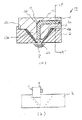
以下、図面を参照して本発明の実施の形態について説明する。図1は、本発明の実施の形態1による近視野光メモリヘッド1の構成を示す側断面図である。図1に示す近視野光メモリヘッド1において、シリコン基板2は、その厚さtを数100μmとしており、その中央部には、表面から裏面に向けて徐々にテーパ状に縮径される逆錐形状のテーパ穴2aが形成されている。このテーパ穴2aの頂点においては、数十ナノメートルの径の微小開口2bが形成されている。イルミネーションモードにおいては、この微小開口2bの近傍に近視野光Pが生成される。
【0030】
反射膜3は、アルミニウム(Al)、クロム(Cr)、金(Au)等の金属膜、または誘電体多層膜等からなり、CVD(Chemical Vapor Deposition)、スパッタ、蒸着等の手法により、テーパ穴2aのテーパ面に形成されている。光ファイバ4は、コア4aおよび該コア4aの周囲を覆うクラッド4bから構成されており、例えば、シングルモード光ファイバである。この光ファイバ4は、レーザ光源(図示略)から射出されたレーザ光Laを伝搬させる。この光ファイバ4において、コア4aの屈折率はクラッド4bの屈折率より大きくなるように設計されている。
【0031】
また、光ファイバ4の先端部4cは、エッチング、機械的研磨、熱引き等の手法により、テーパ穴2aの形状に合致するようにテーパ状に形成されており、テーパ穴2aに嵌合されている。従って、実施の形態1による近視野光メモリヘッド1においては、コア4aの端面と微小開口2bとの距離が従来のものと比較して非常に短くなるように構成されている。
【0032】
上記した構成において、近視野光メモリヘッド1を記録媒体の記録再生に適用する場合には、近視野光メモリヘッド1の下方に図示しない記録媒体が配設される。この記録媒体は、例えば円盤状の平面基板であり、相変化記録方式を適用できる材料からなり、局所的な光の照射による情報記録を可能とする。また、記録・再生中において、記録媒体は、図示しない駆動機構により高速回転される。
【0033】
さらに、この場合には、微小開口2b近傍に生成される近視野光Pを記録媒体に作用させるために、微小開口2bと記録媒体の記録面との間を微小開口2bの径程度まで近接させる必要がある。そこで、この例では、近視野光メモリヘッド1と記録媒体との間に潤滑剤を充填し、この潤滑剤の表面張力を利用して近視野光メモリヘッド1と記録媒体の記録面との距離を十分に小さく維持する。また、上記した潤滑剤は、高速回転中に生じる記録媒体の回転軸方向の撓みに近視野光メモリヘッド1の位置を追従させる役目を果たしている。あるいは、ハードディスクで用いられているフライングヘッドの機構を利用することにより、微小開口2bと記録媒体との距離を十分小さく維持することも可能である。
【0034】
このような状態において、図示しない近視野光メモリヘッド制御機構によって、近視野光メモリヘッド1の微小開口2bが、記録媒体の記録面における所望の位置に配置されるように、近視野光メモリヘッド1の位置が制御される。続いて、図示しないレーザ光源から射出されたレーザ光Laが光ファイバ4のコア4aの入射端面に入射されると、該レーザ光Laは、コア4a内を同図下方向に伝搬した後、コア4aの端面から微小開口2bへ向けて空間光として放射される。
【0035】
これにより、微小開口2bの近傍、言い換えれば、微小開口2bと記録媒体の記録面との間の微小空間に近視野光Pが生成される。ここで、上記空間光が伝搬中においては、コア4aの端面と微小開口2bとの間の距離が非常に短いため、上記空間光と微小開口2bとのカップリングロスが従来のものと比較して小さくなる。
【0036】
そして、上記近視野光Pと記録媒体の記録面との相互作用によって生じた伝搬光が、記録面の記録状態に依存した強度や位相等の特性を伴って図示しない受光素子へと導かれて電気信号に変換され、図示しない信号線を介して同じく図示しない信号処理部によって情報記録部の記録状態が判断される。
【0037】
以上説明したように、上述した実施の形態1による近視野光メモリヘッド1によれば、光ファイバ4の先端部4cをテーパ状に形成することで、コア4aの端面と微小開口2bとの間の距離を非常に小さくするように構成したので、従来のものと比較して、空間光の伝搬距離が短くなるため、空間光と微小開口2bとのカップリングロスを低減することができる。
【0038】
従って、上述した実施の形態1による近視野光メモリヘッド1によれば、上記カップリングロスが小さい分、従来のものと比較して、イルミネーションモードにおける近視野光の光強度および生成効率、コレクションモードにおける近視野光散乱による伝搬光の光強度および検出効率をともに高めることができるとともに、微小開口における熱の発生量を少なくすることができる。
【0039】
なお、上述した実施の形態1による近視野光メモリヘッド1においては、光ファイバ4を直線状に配設した例について説明したが、光ファイバ4の先端部4cから曲げて配設し、先端部4c以外の部分をシリコン基板2に、例えばUV接着剤によって接着するように構成してもよい。この場合には、光ファイバ4の配設位置を近視野光メモリヘッド1の形状に応じて変更することができるので、近視野光メモリヘッド1の小型化が図れる。
【0040】
(実施の形態2)
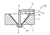
図2(a)は、本発明の実施の形態2による近視野光メモリヘッド10の構成を示す側断面図である。図2(a)において、図1の各部に対応する部分には同一の符号を付けその説明を省略する。
【0041】
図2(a)においては、図1に示す光ファイバ4に代えて、光導波路12を有したガラス基板11が設けられている。ガラス基板の代わりにシリコン基板などを用いても良い。なお、この説明においては、図2に示す反射膜13は設けられていないものとする。
【0042】
図2(a)に示すガラス基板11は、裏面上の突出部11aを有している。この突出部11aは、一部がガラス基板11の側面と一致した側面を有し、先端部を除く他部がシリコン基板2のテーパ穴2aの形状に合致するようにテーパ状に形成されている。また、突出部11aは、その端面(先端部)と微小開口2bとの間の距離が非常に小さくなるようにして形成されている。
【0043】
また、ガラス基板11は、シリコン基板2に形成された嵌合部2cに、UV接着剤または陽極接合等によって接合されている。ここで、上記陽極接合とは、ガラス基板11とシリコン基板2との間に高電圧を印加することにより、境界面において生じるイオン結合による結合をいう。
【0044】
図2(b)は、図2(a)のA−A’線における断面図である。光導波路12は、図示しないコアとクラッドからなり、図2(b)に示すようにガラス基板11の側面上に、かつ図2(a)に示すように逆L字状に設けられている。また、光導波路12の端面は、突出部11aの端面とほぼ一致する位置にある。
【0045】
ここで、突出部11aの端面とほぼ一致した光導波路12の端面は、その中心部が微小開口2bの中心軸上に位置するように配置される。すなわち、光導波路12は、微小開口2bの近傍にまで配置されたガラス基板11、特にその突出部11aを支持体として、端面と微小開口2bとの間の距離が、非常に短くなるように配設される。
【0046】
上記構成において、図示しないレーザ光発生装置により発生されたレーザ光Laが光導波路12の入射端面に入射されると、該レーザ光Laは、光導波路12内を伝搬した後、光導波路12の端面から微小開口2bへ向けて空間光として放射される。これにより、前述した動作と同様にして、微小開口2bの近傍に近視野光Pが生成される。
【0047】
ここで、上記した空間光が伝搬中においては、光導波路12の端面と微小開口2bとの間の距離が非常に短いため、前述した実施の形態1による近視野光メモリヘッド1(図1参照)と同様にして、上記空間光と微小開口2bとのカップリングロスが従来のものと比較して小さくなる。従って、上述した実施の形態2による近視野光メモリヘッド10によれば、実施の形態1による近視野光メモリヘッド1と同様の効果が得られる。
【0048】
なお、上述した実施の形態2による近視野光メモリヘッド10においては、光導波路12の屈曲部12aに、レーザ光Laを端面(微小開口2b)方向へ反射させる反射膜13を設ける構成としてもよい。この場合には、反射膜13によりレーザ光Laが効率よく端面(微小開口2b)へ導かれるので、屈曲部12aにおける光伝搬損失を低減することができる。
【0049】
(実施の形態3)
図3は、本発明の実施の形態3による近視野光メモリヘッド20の構成を示す側断面図である。図3において、図2の各部に対応する部分には同一の符号を付ける。図3においては、図2に示すガラス基板11に代えて、支持部材21が設けられている。すなわち、図3において、光導波路12は、支持部材21を介してシリコン基板2の表面に直接、支持されている。また、光導波路12は逆L字状になるように、レーザ光による熱変形、ポリイミドなどの膜応力により、曲成されている。
【0050】
従って、上記実施の形態3による近視野光メモリヘッド20によれば、前述した近視野光メモリヘッド10(図2参照)と比較して、ガラス基板11が無い分、容積を小さくすることができることから、結果的に小型化を図ることができる。
【0051】
(実施の形態4)
図4(a)は、本発明の実施の形態4による近視野光メモリヘッド30の構成を示す側断面図であり、図4(b)は、上記近視野光メモリヘッド30の構成を示す平面図である。図4(a)および(b)において、図1の各部に対応する部分には同一の符号を付けその説明を省略する。
【0052】
図4(a)においては、図1に示す光ファイバ4に代えて、光導波路31および反射膜32が設けられている。図4(a)に示す光導波路31は、テーパ穴2aのテーパ面に沿いかつ断面がV字状になるように、上記テーパ面に形成された薄膜光導波路であり、コア31aおよびクラッド31bから構成されている。また、光導波路31の表面には、前述したアルミニウム(Al)、クロム(Cr)、金(Au)等の金属膜や、誘電体多層膜からなる反射膜32が、CVD、スパッタ、蒸着等の手法により薄膜形成されている。
【0053】
上記した構成において、図示しないレーザ光発生装置により発生されたレーザ光Laが光導波路31の入射端面に入射されると、該レーザ光Laは、光導波路31内を伝搬した後、光導波路31内を図4(b)に示す矢印A1方向、すなわち、微小開口2b方向へ伝搬する。そして、レーザ光Laが光導波路31の屈曲部31cに到達すると、その一部が微小開口2bへ放射される。これにより、微小開口2b近傍には、近視野光Pが生成される。
【0054】
一方、屈曲部31cから放射されなかったレーザ光Laの残りの部分は、図4(b)に示す矢印A2方向、言い換えれば、光導波路31の端部31d方向へ伝搬する。そして、上記残りの部分のレーザ光Laが端部31dに到達すると、端部31dにおいては、上記レーザ光Laが反射膜32の反射部32aにより図4(b)に示す矢印A3方向、言い換えれば、端部31dから屈曲部31cへ向けて伝搬する。
【0055】
そして、反射部32aにより反射されたレーザ光Laが屈曲部31cに到達すると、上記レーザ光Laは、微小開口2bへ放射される。これにより、微小開口2b近傍には、近視野光Pが生成される。
【0056】
すなわち、実施の形態4による近視野光メモリヘッド30においては、屈曲部31cから端部31dへ向けて伝搬したレーザ光Laを、反射部32aにより再び屈曲部31cへ反射させるように構成したので、近視野光Pの光強度を高めることが可能となる。
【0057】
なお、上述した実施の形態4による近視野光メモリヘッド30においては、反射部32aを曲面形成するか、または反射部32aにグレーディングを施すことにより、反射部32aを凹面鏡として作用させてもよい。この場合には、反射部32aにより反射されたレーザ光Laが屈曲部31c(微小開口2b)へ向けて集光されるので、さらに近視野光Pの光強度を高めることができる。
【0058】
以上本発明の実施の形態1〜4について詳述してきたが、具体的な構成はこれらの実施の形態1〜4に限られるものではなく本発明の要旨を逸脱しない範囲の設計変更等があっても本発明に含まれる。例えば、上述した実施の形態1〜3においては、図1に示す光ファイバ4(コア4a)、図2に示す光導波路12および図3に示す光導波路12の各端面を球状に形成して、レンズ機能を持たせるように構成してもよい。この場合には、微小開口2bへの集光率が高まるので、近視野光Pの光強度を高めることができる。
【0059】
また、実施の形態1〜4において、近視野光を生成するのに用いる光は、レーザ光のように特にコヒーレントな光である必要はなく、インコヒーレントな光であるLED等から射出される光を用いてもよい。
【0060】
【発明の効果】
以上説明したように、請求項1にかかる発明によれば、光ファイバの先端部分が平面基板の穴に嵌合されると、光ファイバの出射端面と微小開口との間の距離が非常に短くなるように構成したので、空間光が伝搬する距離が非常に短くなることから、空間結合時のカップリングロスが、従来のものと比較して非常に小さく抑えられる。従って、請求項1にかかる発明によれば、カップリングロスが低減されることから、近視野光の光強度・出射効率を高めることができる。さらに、請求項1にかかる発明によれば、レーザ光の光強度を高める必要がないので、発生する熱量を低減させることができる。また、消費電力を小さくすることができる。
【0061】
また、請求項2にかかる発明によれば、光ファイバの先端面から出射されるレーザ光が微小開口へ向けて集光されつつ伝搬するため、微小開口に出射されたレーザ光の強度が高まり、ひいては微小開口に生成される近視野光の光強度をさらに高めることができる。
【0062】
また、請求項3にかかる発明によれば、光導波路の端面と微小開口との間の距離が非常に短くなるように構成したので、空間光が伝搬する距離が非常に短くなることから、空間結合時のカップリングロスが、従来のものと比較して非常に小さく抑えられる。従って、請求項3にかかる発明によれば、カップリングロスが低減されることから、近視野光の光強度・出射効率を高めることができるとともに、発生する熱量を低減させることができる。また、消費電力を小さくすることができる。
【0063】
また、請求項4にかかる発明によれば、光導波路を単に支持部材を介して平面基板に支持するように構成したので、請求項1にかかる発明と同様の効果を奏するとともに、構成を簡略化することができ、ひいては小型化を図ることができる。
【0064】
また、請求項5にかかる発明によれば、光導波路の端面から出射されるレーザ光が微小開口へ向けて集光されつつ伝搬するため、微小開口に出射されたレーザ光の強度が高まり、ひいては微小開口に生成される近視野光の光強度をさらに高めることができる。
【0065】
また、請求項6にかかる発明によれば、屈曲部から光導波路の反射膜へ向けて伝搬したレーザ光を、反射膜により再び屈曲部へ反射させるように構成したので、近視野光の光強度を高めることができる。
【0066】
また、請求項7にかかる発明によれば、反射膜により反射されたレーザ光が屈曲部(微小開口)へ向けて集光されつつ伝搬するように構成した。従って微小開口に出射されたレーザ光の強度をさらに高めることができ、ひいては微小開口に生成される近視野光の光強度をさらに高めることができる。
【図面の簡単な説明】
【図1】本発明の実施の形態1にかかる近視野光メモリヘッド1の構成を示す側断面図である。
【図2】実施の形態2にかかる近視野光メモリヘッド10の構成を示す側断面図である。
【図3】実施の形態3にかかる近視野光メモリヘッドの20構成を示す側断面図である。
【図4】実施の形態4にかかる近視野光メモリヘッド30の構成を示す図である。
【符号の説明】
1,10,20 近視野光メモリヘッド
2 シリコン基板
2a テーパ穴
2b 微小開口
3,13,32 反射膜
4 光ファイバ
4c 先端部
11 ガラス基板
12,31 光導波路
21 支持部材[0001]
BACKGROUND OF THE INVENTION
The present invention relates to a near-field optical memory head suitable for reproducing and recording high-density information on a recording medium (optical memory) using near-field light (including both near-field and far-field).
[0002]
[Prior art]
Conventionally, a scanning probe microscope (SPM) represented by a scanning tunneling microscope (STM) or an atomic force microscope (AFM) has been used to observe a minute region on the order of nanometers on a sample surface. SPM scans a sample surface with a probe with a sharpened tip, and observes the interaction between the probe and the sample surface, such as tunneling current and atomic force, with an image of resolution depending on the probe tip shape. However, restrictions on the sample to be observed are relatively severe.
[0003]
Therefore, a near-field microscope that enables observation of minute areas on the sample surface by using propagation light and observing the interaction between the near-field light generated on the sample surface and the probe. Is attracting attention.
[0004]
The near-field microscope described above irradiates the surface of the sample with propagating light to generate near-field light, scatters the generated near-field light with a probe with a sharpened tip, and the scattered light is propagated in the past. By processing in the same way as the light detection, the limit of the observation resolution by the conventional optical microscope is overcome, and a smaller area can be observed. Furthermore, the near-field microscope enables the observation of the optical physical properties of the sample in a minute region by sweeping the wavelength of the light applied to the sample surface.
[0005]
In the near-field microscope, an optical fiber probe having a configuration in which an optical fiber is sharpened and its periphery is coated with metal and a minute opening is provided at the tip thereof is used. This optical fiber probe serves to guide the scattered light generated by interacting the minute opening with near-field light to the photodetector through the inside thereof.
[0006]
The near-field microscope also introduces light toward the sample through the optical fiber probe to generate near-field light at the microscopic aperture of the optical fiber probe, and the interaction between the near-field light and the microstructure on the sample surface. It is also possible to conduct the surface observation by guiding the scattered light generated by the above to a photodetector using a condensing system further added.
[0007]
Furthermore, the near-field microscope technology is not only used as a microscope, but also by introducing relatively high intensity light toward the sample through the optical fiber probe, so that the near-field with a high energy density is introduced into the microscopic aperture of the optical fiber probe. The present invention can also be applied to high-density information recording / reproducing techniques that generate light and locally change the structure or physical properties of the sample surface by the near-field light.
[0008]
Here, as the optical fiber probe described above, for example, as disclosed in US Pat. No. 5,294,790, an opening is formed through the silicon substrate by a semiconductor manufacturing technique such as photolithography, and one of the silicon substrates is formed. A cantilever type optical probe has been proposed in which an insulating film is formed on the surface, and a conical optical waveguide layer is formed on the insulating film on the side opposite to the opening. In this cantilever type optical probe, light can be transmitted through a minute opening formed by inserting an optical fiber into the opening and coating the portion other than the tip of the optical waveguide layer with a metal film.
[0009]
Further, conventionally, it has been proposed to use a flat probe having no sharpened tip like the above-described optical fiber probe. This planar probe is a silicon substrate in which a minute opening having an inverted pyramid structure is formed by anisotropic etching, and its apex is penetrated with a diameter of several tens of nanometers. In addition, in the planar probe, a lens is provided in the inverted pyramid structure portion, and the intensity of near-field light generated in the minute aperture is increased by condensing the laser light to the minute aperture by the lens. ing. This planar probe is used as a near-field optical memory head suitable for reproduction and recording of an optical information recording medium (optical memory) using near-field light.
[0010]
[Problems to be solved by the invention]
By the way, in the conventional cantilever type optical probe, an optical fiber is inserted into the opening to receive the scattered light from the optical waveguide layer or introduce the propagation light into the optical waveguide layer. It was not possible to propagate a sufficient amount of light between the optical fiber and the optical fiber without loss. For example, when the near-field light is emitted from the minute opening at the tip of the optical waveguide layer, the efficiency of the generated near-field light (= light intensity of the near-field light / incident light energy) is as follows. At most, it is on the order of 10 −6 , and most of the light energy is converted into heat energy, and there is a problem that wasteful energy is consumed.
[0011]
Here, the factors affecting the generation efficiency of the near-field light described above are the shape in the vicinity of the minute aperture (particularly, the portion where the aperture width is equal to or smaller than the wavelength of visible light), and the surface of the optical waveguide layer. The reflectance of the metal film, the condensing rate of the propagation light to the minute aperture, and the like are conceivable.
[0012]
Therefore, in the cantilever type optical probe, a method of increasing the light intensity of the light source that irradiates the minute aperture in order to obtain sufficient light intensity of near-field light can be considered, but this method generates a large amount of heat. Therefore, the structural member (metal film) or the like may be damaged, which is not realistic.
[0013]
Furthermore, in the conventional flat probe, the coupling end loss is very large because the core end face of the optical fiber and the minute aperture are spatially coupled via a lens. Considering this, light loss is further increased, and the light intensity and generation efficiency of near-field light in the illumination mode and the light intensity and detection efficiency of propagation light due to near-field light scattering in the collection mode are both reduced.
[0014]
The present invention has been made under such a background, and improves both the light intensity and generation efficiency of near-field light in the illumination mode and the light intensity and detection efficiency of propagation light due to near-field light scattering in the collection mode. In particular, an object of the present invention is to provide a near-field optical memory head capable of reducing the amount of heat generated in a minute aperture in an illumination mode.
[0015]
[Means for Solving the Problems]
In order to achieve the above object, the invention according to claim 1 is a near-field optical memory head that records and / or reproduces information on a recording medium using near-field light. Is formed in a tapered shape so that the top portion of the flat substrate has a minute opening, and the tip portion has substantially the same shape as the shape of the inverted conical hole of the flat substrate, and The tip portion includes an optical fiber fitted in the hole.
[0016]
According to the first aspect of the present invention, when the tip portion of the optical fiber is fitted into the hole of the flat substrate, the distance between the emission end face of the optical fiber and the minute opening becomes very short. In this state, when the laser light is incident on the incident end face of the optical fiber, the laser light propagates through the optical fiber, and then is emitted as spatial light from the exit end face toward the minute opening. Near-field light is generated. Since the distance through which this spatial light propagates is very short, the coupling loss at the time of spatial coupling can be suppressed to be very small as compared with the conventional one, so that the light propagation loss is reduced.
[0017]
According to a second aspect of the present invention, in the near-field optical memory head according to the first aspect, the tip surface of the optical fiber is substantially spherical.
[0018]
According to the invention of
[0019]
According to a third aspect of the present invention, in a near-field optical memory head that records and / or reproduces information on a recording medium using near-field light, at least one inverted conical hole has a minute opening at the top. A flat substrate formed so as to penetrate through the substrate, and formed in a tapered shape so as to protrude on the back surface and a part of the shape is substantially the same as a part of the shape of the inverted conical hole of the flat substrate. A substrate provided so that the protruding portion is fitted into an inverted conical hole of the flat substrate, and the substrate and the end surface are positioned on the end surface of the protruding portion. And an optical waveguide disposed on a side surface of the projecting portion.
[0020]
According to the invention of
[0021]
According to a fourth aspect of the present invention, in the near-field optical memory head that records and / or reproduces information on the recording medium using near-field light, at least one inverted conical hole has a minute opening at the top. A planar substrate formed so as to penetrate through the optical waveguide, an optical waveguide disposed so that an end portion thereof is positioned in an inverted conical hole of the planar substrate and an end surface thereof is positioned in the vicinity of the minute opening, and the optical waveguide And a support member that supports the waveguide on the planar substrate.
[0022]
Further, according to the invention of
[0023]
According to a fifth aspect of the present invention, in the near-field optical memory head according to the third or fourth aspect, the end surface of the optical waveguide has a substantially spherical shape.
[0024]
According to the invention of claim 5, since the substantially spherical end surface portion of the optical waveguide serves as a condensing lens, the laser light emitted from the end surface of the optical waveguide is collected toward the minute aperture. Propagating while being illuminated. Therefore, according to the invention concerning Claim 5, the intensity | strength of the laser beam radiate | emitted toward the minute opening increases, and the light intensity of the near-field light produced | generated by a minute opening by extension increases.
[0025]
The invention according to claim 6 is a near-field optical memory head that records and / or reproduces information on a recording medium using near-field light, and at least one inverted conical hole has a minute opening at the top. A flat substrate formed so as to penetrate, and a side portion of the inverted conical hole so that a portion thereof is substantially V-shaped, and a bent portion of the portion is formed in the vicinity of the minute opening. It is characterized by comprising an optical waveguide formed to be positioned and at least a reflection film formed on an end face of the part of the optical waveguide.
[0026]
According to the invention of claim 6, when laser light is incident on the incident end face of the optical waveguide, the laser light propagates toward the bent portion of the optical waveguide. When the laser light reaches the bent portion of the optical waveguide, a part of the laser light is emitted toward the minute aperture, and near-field light is generated in the vicinity of the minute aperture. On the other hand, the remaining laser light in the bent portion propagates toward the end face (reflective film) of the optical waveguide, and is then reflected in the bent portion direction by the reflective film. Then, the reflected laser light is emitted toward the minute opening at the bent portion, and near-field light is generated in the minute opening.
That is, according to the sixth aspect of the invention, the laser light propagated from the bent portion toward the reflective film of the optical waveguide is reflected again to the bent portion by the reflective film, so that the light intensity of near-field light is reduced. Will increase.
[0027]
According to a seventh aspect of the present invention, in the near-field optical memory head according to the sixth aspect, the end surface of the part of the optical waveguide is a concave curved surface.
[0028]
According to the invention of claim 7, since the end face (reflective film) of a part of the optical waveguide serves as a concave mirror, the laser light reflected by the reflective film is directed toward the bent part (micro opening). It propagates while being condensed. Therefore, according to the seventh aspect of the present invention, the intensity of the laser beam emitted toward the minute aperture is increased, and as a result, the light intensity of the near-field light generated at the minute aperture is increased.
[0029]
DETAILED DESCRIPTION OF THE INVENTION
(Embodiment 1)
Embodiments of the present invention will be described below with reference to the drawings. FIG. 1 is a side sectional view showing a configuration of a near-field optical memory head 1 according to Embodiment 1 of the present invention. In the near-field optical memory head 1 shown in FIG. 1, the
[0030]
The
[0031]
The tip 4c of the
[0032]
In the above configuration, when the near-field optical memory head 1 is applied to recording / reproduction of a recording medium, a recording medium (not shown) is disposed below the near-field optical memory head 1. This recording medium is, for example, a disk-shaped flat substrate, made of a material to which a phase change recording method can be applied, and enables information recording by local light irradiation. During recording / reproduction, the recording medium is rotated at a high speed by a drive mechanism (not shown).
[0033]
Further, in this case, in order to cause the near-field light P generated near the
[0034]
In such a state, the near-field optical memory head control mechanism (not shown) positions the near-field optical memory head 1 so that the
[0035]
Thereby, near-field light P is generated in the vicinity of the
[0036]
Then, the propagation light generated by the interaction between the near-field light P and the recording surface of the recording medium is guided to a light receiving element (not shown) with characteristics such as intensity and phase depending on the recording state of the recording surface. It is converted into an electrical signal, and the recording state of the information recording unit is judged by a signal processing unit (not shown) through a signal line (not shown).
[0037]
As described above, according to the near-field optical memory head 1 according to the first embodiment described above, the tip portion 4c of the
[0038]
Therefore, according to the near-field optical memory head 1 according to Embodiment 1 described above, since the coupling loss is small, the near-field light intensity and generation efficiency in the illumination mode and the collection mode are smaller than the conventional one. It is possible to increase both the light intensity and detection efficiency of propagating light due to near-field light scattering, and to reduce the amount of heat generated in the minute aperture.
[0039]
In the near-field optical memory head 1 according to the first embodiment described above, the example in which the
[0040]
(Embodiment 2)
FIG. 2A is a side sectional view showing the configuration of the near-field
[0041]
In FIG. 2A, a glass substrate 11 having an
[0042]
The glass substrate 11 shown to Fig.2 (a) has the protrusion part 11a on a back surface. The protruding portion 11 a has a side surface partially matching the side surface of the glass substrate 11, and is formed in a tapered shape so that the other portion except the tip portion matches the shape of the tapered hole 2 a of the
[0043]
The glass substrate 11 is bonded to the fitting portion 2c formed on the
[0044]
FIG. 2B is a cross-sectional view taken along the line AA ′ in FIG. The
[0045]
Here, the end surface of the
[0046]
In the above configuration, when laser light La generated by a laser light generator (not shown) enters the incident end face of the
[0047]
Here, since the distance between the end face of the
[0048]
In the near-field
[0049]
(Embodiment 3)
FIG. 3 is a side sectional view showing the configuration of the near-field
[0050]
Therefore, according to the near-field
[0051]
(Embodiment 4)
FIG. 4A is a side sectional view showing the configuration of the near-field optical memory head 30 according to
[0052]
In FIG. 4A, an optical waveguide 31 and a
[0053]
In the above configuration, when laser light La generated by a laser light generator (not shown) is incident on the incident end face of the optical waveguide 31, the laser light La propagates in the optical waveguide 31 and then in the optical waveguide 31. Is propagated in the direction of arrow A1 shown in FIG. 4B, that is, in the direction of the
[0054]
On the other hand, the remaining portion of the laser beam La that has not been emitted from the bent portion 31c propagates in the direction of the arrow A2 shown in FIG. 4B, in other words, in the direction of the end portion 31d of the optical waveguide 31. When the remaining portion of the laser beam La reaches the end portion 31d, the laser beam La is reflected at the end portion 31d in the direction of the arrow A3 shown in FIG. , And propagates from the end portion 31d toward the bent portion 31c.
[0055]
When the laser beam La reflected by the reflecting portion 32a reaches the bent portion 31c, the laser beam La is emitted to the
[0056]
That is, the near-field optical memory head 30 according to the fourth embodiment is configured such that the laser light La propagated from the bent portion 31c toward the end portion 31d is reflected again to the bent portion 31c by the reflecting portion 32a. The light intensity of the field light P can be increased.
[0057]
In the near-field optical memory head 30 according to the fourth embodiment described above, the reflecting portion 32a may act as a concave mirror by forming the reflecting portion 32a into a curved surface or grading the reflecting portion 32a. In this case, since the laser beam La reflected by the reflecting portion 32a is collected toward the bent portion 31c (the
[0058]
Although the first to fourth embodiments of the present invention have been described in detail above, the specific configuration is not limited to these first to fourth embodiments, and there are design changes and the like within the scope not departing from the gist of the present invention. Is included in the present invention. For example, in the first to third embodiments described above, the end surfaces of the optical fiber 4 (
[0059]
In the first to fourth embodiments, the light used to generate near-field light does not have to be particularly coherent light like laser light, and is emitted from an LED or the like that is incoherent light. May be used.
[0060]
【The invention's effect】
As described above, according to the first aspect of the present invention, when the tip portion of the optical fiber is fitted into the hole of the flat substrate, the distance between the emission end face of the optical fiber and the minute opening is very short. Since the distance that the spatial light propagates becomes very short, the coupling loss at the time of spatial coupling can be suppressed to be very small as compared with the conventional one. Therefore, according to the first aspect of the present invention, since the coupling loss is reduced, the light intensity and emission efficiency of near-field light can be increased. Furthermore, according to the first aspect of the present invention, since it is not necessary to increase the light intensity of the laser beam, the amount of heat generated can be reduced. In addition, power consumption can be reduced.
[0061]
According to the invention of
[0062]
Further, according to the invention of
[0063]
Further, according to the invention according to
[0064]
According to the invention of claim 5, since the laser beam emitted from the end face of the optical waveguide propagates while being condensed toward the minute aperture, the intensity of the laser beam emitted to the minute aperture is increased, and consequently The light intensity of near-field light generated at the minute aperture can be further increased.
[0065]
According to the sixth aspect of the present invention, the laser light propagated from the bent portion toward the reflection film of the optical waveguide is reflected again to the bent portion by the reflection film. Can be increased.
[0066]
According to the invention of claim 7, the laser beam reflected by the reflecting film is propagated while being condensed toward the bent portion (small opening). Accordingly, it is possible to further increase the intensity of the laser light emitted to the minute aperture, and further increase the light intensity of the near-field light generated in the minute aperture.
[Brief description of the drawings]
FIG. 1 is a side sectional view showing a configuration of a near-field optical memory head 1 according to a first embodiment of the present invention.
FIG. 2 is a side sectional view showing a configuration of a near-field
FIG. 3 is a side sectional view showing a 20 configuration of a near-field optical memory head according to a third embodiment;
FIG. 4 is a diagram showing a configuration of a near-field optical memory head 30 according to a fourth embodiment.
[Explanation of symbols]
1, 10, 20 Near-field
Claims (4)
少なくとも1つの逆錐状の穴がその頂部を微小開口とするように貫通して形成された平面基板と、
裏面上に突出形成されかつその形状の一部が前記平面基板の逆錐状の前記穴の形状の一部と略同形状となるようにテーパ状に形成された突出部を有し、前記突出部が前記平面基板の逆錐状の前記穴に嵌合されるように設けられた基板と、
端面が前記突出部の端面に位置するように、前記基板および前記突出部の側面上に配設された光導波路と、
を備えることを特徴とする近視野光メモリヘッド。In a near-field optical memory head that performs recording and reproduction of information on a recording medium using near-field light,
A planar substrate formed with at least one inverted conical hole penetrating so that the top of the hole has a minute opening;
A protrusion formed on the back surface, and having a protrusion formed in a tapered shape so that a part of the shape is substantially the same as a part of the shape of the inverted conical hole of the flat substrate; A board provided so that a portion is fitted into the hole of the inverted conical shape of the flat board;
An optical waveguide disposed on a side surface of the substrate and the protruding portion such that an end surface is located on an end surface of the protruding portion;
A near-field optical memory head comprising:
少なくとも1つの逆錐状の穴がその頂部を微小開口とするように貫通して形成された平面基板と、
一部分が略V字状になるように前記逆錐状の穴の側面に沿って形成され、かつ該一部分の屈曲部が前記微小開口の近傍に位置して形成される光導波路と、
少なくとも、前記光導波路の前記一部分の端面に形成された反射膜と、
を備えることを特徴とする近視野光メモリヘッド。A near-field optical memory head that uses near-field light to perform at least one of recording and reproduction of information on a recording medium,
A planar substrate formed with at least one inverted conical hole penetrating so that the top of the hole has a minute opening;
An optical waveguide that is formed along the side surface of the inverted conical hole so that a portion thereof is substantially V-shaped, and a bent portion of the portion is formed in the vicinity of the minute opening;
At least a reflective film formed on an end face of the portion of the optical waveguide;
A near-field optical memory head comprising:
Priority Applications (1)
| Application Number | Priority Date | Filing Date | Title |
|---|---|---|---|
| JP36323298A JP4153114B2 (en) | 1998-12-21 | 1998-12-21 | Near-field optical memory head |
Applications Claiming Priority (1)
| Application Number | Priority Date | Filing Date | Title |
|---|---|---|---|
| JP36323298A JP4153114B2 (en) | 1998-12-21 | 1998-12-21 | Near-field optical memory head |
Related Child Applications (1)
| Application Number | Title | Priority Date | Filing Date |
|---|---|---|---|
| JP2008041249A Division JP4339387B2 (en) | 2008-02-22 | 2008-02-22 | Near-field optical memory head |
Publications (3)
| Publication Number | Publication Date |
|---|---|
| JP2000187874A JP2000187874A (en) | 2000-07-04 |
| JP2000187874A5 JP2000187874A5 (en) | 2006-03-23 |
| JP4153114B2 true JP4153114B2 (en) | 2008-09-17 |
Family
ID=18478829
Family Applications (1)
| Application Number | Title | Priority Date | Filing Date |
|---|---|---|---|
| JP36323298A Expired - Fee Related JP4153114B2 (en) | 1998-12-21 | 1998-12-21 | Near-field optical memory head |
Country Status (1)
| Country | Link |
|---|---|
| JP (1) | JP4153114B2 (en) |
Cited By (1)
| Publication number | Priority date | Publication date | Assignee | Title |
|---|---|---|---|---|
| CN111141221A (en) * | 2019-12-16 | 2020-05-12 | 西安交通大学 | Preparation method of optical fiber probe for micro-displacement sensor, micro-displacement sensor and application |
Families Citing this family (1)
| Publication number | Priority date | Publication date | Assignee | Title |
|---|---|---|---|---|
| JP3491043B1 (en) * | 2002-06-11 | 2004-01-26 | 独立行政法人物質・材料研究機構 | Optical fiber probe manufacturing method and fine material processing method |
-
1998
- 1998-12-21 JP JP36323298A patent/JP4153114B2/en not_active Expired - Fee Related
Cited By (1)
| Publication number | Priority date | Publication date | Assignee | Title |
|---|---|---|---|---|
| CN111141221A (en) * | 2019-12-16 | 2020-05-12 | 西安交通大学 | Preparation method of optical fiber probe for micro-displacement sensor, micro-displacement sensor and application |
Also Published As
| Publication number | Publication date |
|---|---|
| JP2000187874A (en) | 2000-07-04 |
Similar Documents
| Publication | Publication Date | Title |
|---|---|---|
| JP4020233B2 (en) | Near-field optical head and manufacturing method thereof | |
| US6408123B1 (en) | Near-field optical probe having surface plasmon polariton waveguide and method of preparing the same as well as microscope, recording/regeneration apparatus and micro-fabrication apparatus using the same | |
| US6881947B2 (en) | Near-field optical probe | |
| JP4094229B2 (en) | Near-field optical head and manufacturing method thereof | |
| US7240541B2 (en) | Optical microcantilever, manufacturing method thereof, and optical microcantilever holder | |
| JP4184570B2 (en) | Information recording / reproducing device | |
| JP4885973B2 (en) | Surface plasmon polariton direction changer, information recording / reproducing head, optically assisted magnetic recording apparatus, and optical circuit | |
| JP2006323908A (en) | Head module | |
| JP2002014030A (en) | Near-field optical probe and its manufacturing method, and near-field optical apparatus using near-field optical probe | |
| JP4024570B2 (en) | Near-field light generating element, near-field light recording device, and near-field light microscope | |
| JP4421742B2 (en) | Optical head | |
| JP2002245659A (en) | Information recording and reproducing device | |
| JP4083330B2 (en) | Near-field optical memory head | |
| JP4601867B2 (en) | Near-field optical head | |
| JP4153114B2 (en) | Near-field optical memory head | |
| JP3267992B2 (en) | Near-field scanning optical microscope and its use | |
| JP4339387B2 (en) | Near-field optical memory head | |
| JP3157083B2 (en) | Optical recording device | |
| JP3592546B2 (en) | High power optical probe and optical system | |
| JP3817498B2 (en) | Manufacturing method of probe having probe for near-field light | |
| JP2010078618A (en) | Optical microcantilever, method of manufacturing the same, and optical microcantilever holder | |
| JP4162317B2 (en) | Near-field optical memory head | |
| JP4610855B2 (en) | Near-field light generating element, near-field light recording device, and near-field light microscope | |
| JP4087034B2 (en) | Near-field optical device and manufacturing method thereof | |
| JP4286418B2 (en) | Near-field optical head |
Legal Events
| Date | Code | Title | Description |
|---|---|---|---|
| RD01 | Notification of change of attorney |
Free format text: JAPANESE INTERMEDIATE CODE: A7421 Effective date: 20040302 |
|
| A521 | Written amendment |
Free format text: JAPANESE INTERMEDIATE CODE: A523 Effective date: 20051117 |
|
| A621 | Written request for application examination |
Free format text: JAPANESE INTERMEDIATE CODE: A621 Effective date: 20051117 |
|
| A977 | Report on retrieval |
Free format text: JAPANESE INTERMEDIATE CODE: A971007 Effective date: 20071219 |
|
| A131 | Notification of reasons for refusal |
Free format text: JAPANESE INTERMEDIATE CODE: A131 Effective date: 20071225 |
|
| A521 | Written amendment |
Free format text: JAPANESE INTERMEDIATE CODE: A523 Effective date: 20080222 |
|
| TRDD | Decision of grant or rejection written | ||
| A01 | Written decision to grant a patent or to grant a registration (utility model) |
Free format text: JAPANESE INTERMEDIATE CODE: A01 Effective date: 20080701 |
|
| A01 | Written decision to grant a patent or to grant a registration (utility model) |
Free format text: JAPANESE INTERMEDIATE CODE: A01 |
|
| A61 | First payment of annual fees (during grant procedure) |
Free format text: JAPANESE INTERMEDIATE CODE: A61 Effective date: 20080703 |
|
| R150 | Certificate of patent or registration of utility model |
Free format text: JAPANESE INTERMEDIATE CODE: R150 |
|
| FPAY | Renewal fee payment (event date is renewal date of database) |
Free format text: PAYMENT UNTIL: 20110711 Year of fee payment: 3 |
|
| RD01 | Notification of change of attorney |
Free format text: JAPANESE INTERMEDIATE CODE: A7421 Effective date: 20091108 |
|
| FPAY | Renewal fee payment (event date is renewal date of database) |
Free format text: PAYMENT UNTIL: 20110711 Year of fee payment: 3 |
|
| RD03 | Notification of appointment of power of attorney |
Free format text: JAPANESE INTERMEDIATE CODE: R3D03 |
|
| FPAY | Renewal fee payment (event date is renewal date of database) |
Free format text: PAYMENT UNTIL: 20110711 Year of fee payment: 3 |
|
| FPAY | Renewal fee payment (event date is renewal date of database) |
Free format text: PAYMENT UNTIL: 20120711 Year of fee payment: 4 |
|
| FPAY | Renewal fee payment (event date is renewal date of database) |
Free format text: PAYMENT UNTIL: 20130711 Year of fee payment: 5 |
|
| LAPS | Cancellation because of no payment of annual fees |