JP4150922B2 - Method for forming laminate - Google Patents
Method for forming laminate Download PDFInfo
- Publication number
- JP4150922B2 JP4150922B2 JP2003351843A JP2003351843A JP4150922B2 JP 4150922 B2 JP4150922 B2 JP 4150922B2 JP 2003351843 A JP2003351843 A JP 2003351843A JP 2003351843 A JP2003351843 A JP 2003351843A JP 4150922 B2 JP4150922 B2 JP 4150922B2
- Authority
- JP
- Japan
- Prior art keywords
- layer
- coating
- acid
- coating film
- mono
- Prior art date
- Legal status (The legal status is an assumption and is not a legal conclusion. Google has not performed a legal analysis and makes no representation as to the accuracy of the status listed.)
- Expired - Fee Related
Links
Images


Description
本発明は、積層体、積層体の形成方法、絶縁層ならびに半導体基板に関し、さらに詳しくは、半導体装置における層間絶縁層材料として使用でき、加工プロセス時に用いるプラズマに対する耐性に優れた積層体およびその形成方法、前記積層体からなる絶縁層、ならびに前記絶縁層が形成された半導体基板に関する。 The present invention relates to a laminated body, a method for forming a laminated body, an insulating layer, and a semiconductor substrate, and more specifically, a laminated body that can be used as an interlayer insulating layer material in a semiconductor device and has excellent resistance to plasma used during a processing process, and its formation The present invention relates to a method, an insulating layer made of the laminate, and a semiconductor substrate on which the insulating layer is formed.
従来、半導体装置などにおける層間絶縁層として、CVD法などの真空プロセスによって形成されたシリカ(SiO2)膜が多用されている。そして、近年、より均一な層間絶縁層を形成することを目的として、SOG(Spin on Glass)膜と呼ばれるテトラアルコキシランの加水分解生成物を主成分とする塗布型の絶縁層が使用されるようになってきている。また、半導体装置などの高集積化に伴い、有機SOGと呼ばれるポリオルガノシロキサンを主成分とする低比誘電率の層間絶縁層が開発されている。 Conventionally, a silica (SiO 2 ) film formed by a vacuum process such as a CVD method is frequently used as an interlayer insulating layer in a semiconductor device or the like. In recent years, for the purpose of forming a more uniform interlayer insulating layer, a coating type insulating layer called a SOG (Spin on Glass) film containing a hydrolysis product of tetraalkoxylane as a main component has been used. It is becoming. In addition, with high integration of semiconductor devices and the like, an interlayer insulating layer having a low relative dielectric constant, which is mainly composed of polyorganosiloxane called organic SOG, has been developed.
また、近年、半導体装置などのさらなる高集積化や多層化に伴い、導体間の電気絶縁性のさらなる向上が要求されており、したがって、より低比誘電率で機械的強度に優れた層間絶縁層材料が求められるようになっている(例えば、特許文献1および2参照)。
本発明の目的は、半導体装置における層間絶縁層材料として使用でき、加工プロセス時に用いるプラズマに対する耐性に優れた積層体およびその形成方法を提供することにある。 An object of the present invention is to provide a laminate that can be used as an interlayer insulating layer material in a semiconductor device and has excellent resistance to plasma used during a processing process, and a method for forming the same.
また、本発明の目的は、前記積層体からなる絶縁層、ならびに前記絶縁層が形成された半導体基板を提供することにある。 Another object of the present invention is to provide an insulating layer made of the laminate and a semiconductor substrate on which the insulating layer is formed.
(1)本発明の積層体は、
アルコキシシラン加水分解縮合物を硬化して得られ、比誘電率が2.5以下である第1の層と、アルコキシシラン加水分解縮合物を硬化して得られ、比誘電率が2.5を超える第2の層とが積層されてなり、前記第1の層の比誘電率と前記第2の層の比誘電率との差が0.3以上であり、かつ前記第1の層と前記第2の層との間に、Siを含有し、かつO、C、N、Hの群から選ばれる少なくとも1種の元素を含有する第3の層が形成されている。
(1) The laminate of the present invention is
A first layer having a relative dielectric constant of 2.5 or less, obtained by curing an alkoxysilane hydrolyzed condensate, and obtained by curing an alkoxysilane hydrolyzed condensate having a relative dielectric constant of 2.5. And a second dielectric layer that exceeds the second dielectric layer, wherein a difference between a relative dielectric constant of the first layer and a relative dielectric constant of the second layer is 0.3 or more, and the first layer and the second layer A third layer containing Si and containing at least one element selected from the group of O, C, N, and H is formed between the second layer and the second layer.
ここで、前記アルコキシシラン加水分解縮合物が、下記一般式(1)で表される化合物、下記一般式(2)で表される化合物および下記一般式(3)で表される化合物の群から選ばれた少なくとも1種のシラン化合物を加水分解縮合したものであることができる。 Here, the alkoxysilane hydrolysis condensate is a compound represented by the following general formula (1), a compound represented by the following general formula (2), and a compound represented by the following general formula (3). It may be a product obtained by hydrolytic condensation of at least one selected silane compound.
RaSi(OR1)4−a ・・・・・(1)
〔式中、Rは水素原子、フッ素原子または1価の有機基を示し、R1は1価の有機基を示し、aは1〜2の整数を表す。〕
Si(OR2)4 ・・・・・(2)
〔式中、R2は1価の有機基を示す。〕
R3 b(R4O)3−bSi−(R7)d−Si(OR5)3−cR6 c ・・・・・(3)
〔式中、R3〜R6は同一または異なり、それぞれ1価の有機基を示し、bおよびcは同一または異なり、0〜2の数を示し、R7は酸素原子、フェニレン基または−(CH2)n−で表される基(ここで、nは1〜6の整数を表す)、dは0または1を表す。〕
R a Si (OR 1 ) 4-a (1)
[Wherein, R represents a hydrogen atom, a fluorine atom or a monovalent organic group, R 1 represents a monovalent organic group, and a represents an integer of 1 to 2. ]
Si (OR 2 ) 4 (2)
[Wherein R 2 represents a monovalent organic group. ]
R 3 b (R 4 O) 3-b Si- (R 7) d -Si (OR 5) 3-c R 6 c ····· (3)
[Wherein, R 3 to R 6 are the same or different and each represents a monovalent organic group, b and c are the same or different and represent a number of 0 to 2, and R 7 represents an oxygen atom, a phenylene group or-( CH 2) n - group represented by (wherein, n is an integer of 1 to 6), d represents 0 or 1. ]
(2)本発明の積層体の形成方法は、
(a)アルコキシシラン加水分解縮合物を含む塗布液を基体上に塗布し、乾燥して第1の塗膜を形成し、
(b)アルコキシシラン加水分解縮合物を含む塗布液を塗布して第3の塗膜を形成し、および
(c)前記第3の塗膜の上方に、前記アルコキシシラン加水分解縮合物を含む塗布液を塗布して第2の塗膜を形成した後、前記第1、第2および第3の塗膜を加熱硬化することにより、比誘電率が2.5以下である第1の層と、比誘電率が2.5を超える第2の層と、前記第1の層と前記第2の層との間に、Siを含有し、かつO、C、N、Hの群から選ばれる少なくとも1種の元素を含有する第3の層とを含む積層体を形成すること、を含む。なお、本願において、「基体」とは、第1の層が形成される面を有する物をいう。「基体」としては、例えば半導体基板、絶縁層、配線層が例示できる。
(2) The method for forming the laminate of the present invention includes:
(A) A coating solution containing an alkoxysilane hydrolysis condensate is applied onto a substrate and dried to form a first coating film;
(B) applying a coating solution containing an alkoxysilane hydrolysis condensate to form a third coating film; and (c) an application containing the alkoxysilane hydrolysis condensate above the third coating film. After the liquid is applied to form the second coating film, the first, second, and third coating films are heated and cured, whereby the first layer having a relative dielectric constant of 2.5 or less, A second layer having a relative dielectric constant exceeding 2.5, and between the first layer and the second layer, containing Si and at least selected from the group of O, C, N, and H Forming a laminate including a third layer containing one kind of element. In the present application, the “base” refers to an object having a surface on which the first layer is formed. Examples of the “base” include a semiconductor substrate, an insulating layer, and a wiring layer.
また、本発明の積層体の形成方法は、
(a)アルコキシシラン加水分解縮合物を含む塗布液を基体上に塗布し、乾燥して第1の塗膜を形成し、
(b)アルコキシシラン加水分解縮合物を含む塗布液を塗布して第3の塗膜を形成し、および
(c)前記第3の塗膜の上方に、アルコキシシラン加水分解縮合物を含む塗布液を塗布して第2の塗膜を形成した後、前記第1、第2および第3の塗膜を電子線もしくは紫外線硬化することにより、比誘電率が2.5以下である第1の層と、比誘電率が2.5を超える第2の層と、前記第1の層と前記第2の層との間に、Siを含有し、かつO、C、N、Hの群から選ばれる少なくとも1種の元素を含有する第3の層とを含む積層体を形成すること、を含む。
Moreover, the method for forming the laminate of the present invention includes:
(A) A coating solution containing an alkoxysilane hydrolysis condensate is applied onto a substrate and dried to form a first coating film;
(B) A coating liquid containing an alkoxysilane hydrolysis condensate is applied to form a third coating film, and (c) a coating liquid containing an alkoxysilane hydrolysis condensate above the third coating film. Is applied to form a second coating film, and then the first, second, and third coating films are cured with an electron beam or an ultraviolet ray so that the first dielectric layer has a relative dielectric constant of 2.5 or less. And a second layer having a relative dielectric constant exceeding 2.5, and containing Si between the first layer and the second layer, and selected from the group of O, C, N, and H Forming a laminated body including a third layer containing at least one kind of element.
(3)本発明の絶縁層は前記積層体からなる。また、本発明の半導体基板は前記絶縁層が形成されている。 (3) The insulating layer of this invention consists of the said laminated body. Further, the insulating layer is formed on the semiconductor substrate of the present invention.
本発明の積層体によれば、前記第2の層が前記第1の層の上方に形成され、前記第1の層と前記第2の層との間に前記第3の層が設けられていることにより、加工プロセス(例えば絶縁層やハードマスク層の成膜工程ならびにエッチング工程)時に使用されるプラズマによって前記第1の層にもたらされるダメージを軽減することができる。また、前記第1、第2および第3の層はそれぞれ、アルコキシシラン加水分解縮合物を含む塗布液を塗布して得られた塗膜(第1の塗膜、第2の塗膜および第3の塗膜)を硬化させて形成することができる。これにより、前記第1、第2の層および第3の層は、例えばCVD法により形成された絶縁層と比較して、面内均一性に優れ、かつ例えば10〜100nmの絶縁層においても100nm以上の絶縁層と同様に均一である。 According to the laminate of the present invention, the second layer is formed above the first layer, and the third layer is provided between the first layer and the second layer. Accordingly, damage caused to the first layer by plasma used in a processing process (for example, a film formation process and an etching process of an insulating layer and a hard mask layer) can be reduced. Each of the first, second and third layers is a coating obtained by applying a coating solution containing an alkoxysilane hydrolysis condensate (first coating, second coating and third coating). Can be formed by curing. Thereby, the first, second and third layers are excellent in in-plane uniformity as compared with an insulating layer formed by, for example, a CVD method, and 100 nm even in an insulating layer of 10 to 100 nm, for example. Similar to the above insulating layer, it is uniform.
また、本発明の積層体の形成方法によれば、低誘電率であり、かつダメージが低減された積層体を簡便な方法にて形成することができる。 Moreover, according to the method for forming a laminate of the present invention, a laminate having a low dielectric constant and reduced damage can be formed by a simple method.
また、本発明の絶縁層は前記積層体からなることにより、例えば本発明の絶縁層が半導体装置の層間絶縁層として使用される場合、配線間の寄生容量が低減された半導体装置を得ることができる。 In addition, since the insulating layer of the present invention is composed of the stacked body, for example, when the insulating layer of the present invention is used as an interlayer insulating layer of a semiconductor device, a semiconductor device with reduced parasitic capacitance between wirings can be obtained. it can.
さらに、本発明の半導体基板によれば、前記絶縁層が形成されていることにより、配線間の寄生容量が低減された半導体装置を得ることができる。 Furthermore, according to the semiconductor substrate of the present invention, a semiconductor device with reduced parasitic capacitance between wirings can be obtained by forming the insulating layer.
以下、本発明の一実施の形態の積層体およびその形成方法、前記積層体からなる絶縁層、ならびに前記絶縁層が形成された半導体基板について具体的に説明する。 Hereinafter, a laminate and a method for forming the laminate, an insulating layer made of the laminate, and a semiconductor substrate on which the insulating layer is formed according to an embodiment of the present invention will be specifically described.
[積層体]
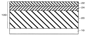
図1は、本発明の一実施の形態の積層体100を模式的に示す断面図である。本実施の形態の積層体100は、図1に示すように、第1の層20および第2の層22が順に積層されて構成されている。また、第1の層20と第2の層22との間には、第3の層24が形成されている。すなわち、この積層体100においては、第1の層20は基体10上に形成され、第2の層22は第3の層24上に形成されている。
[Laminate]
FIG. 1 is a cross-sectional view schematically showing a
第1の層20、第2の層22および第3の層24はいずれも、アルコキシシラン加水分解縮合物を硬化して得られる。第1の層20、第2の層22および第3の層24の詳しい材質については後述する。第1の層20は低比誘電率材料からなる。このため、第1の層20は、プラズマを用いた加工プロセス中で発生する各種反応性イオンにより、化学的および物理的ダメージを受けやすい。このダメージを低減するために、第1の層20の上には、第1の層20より比誘電率が大きい第2の層22が積層されている。この第2の層22によって、各種反応性イオンを遮蔽することができる。
The
上述のプラズマを用いた加工プロセスとしては、プラズマを用いた処理であり、特に限定されるわけではないが、例えばプラズマエッチング、プラズマアッシング、プラズマCVD法、プラズマドーピング、プラズマを用いた表面処理、プラズマアニール、プラズマ酸化等が挙げられる。 The processing process using plasma is a process using plasma, and is not particularly limited. For example, plasma etching, plasma ashing, plasma CVD, plasma doping, surface treatment using plasma, plasma Annealing, plasma oxidation, etc. are mentioned.
第1の層20の比誘電率は2.5以下であり、さらには2.2〜2.5であることが好ましい。第1の層20の比誘電率が2.5を超えると、導体間の電気絶縁性を十分に確保できないことがある。また、第2の層22の比誘電率は2.5を超え、さらには2.7〜3.0であることが好ましい。第2の層22の比誘電率が2.5以下であると、プラズマを用いた加工プロセス時において、第2の層22が各種反応性イオンを十分遮蔽できず、第1の層20へのプラズマによるダメージを十分に低減できないことがある。
The relative dielectric constant of the
また、第1の層20の比誘電率と第2の層22の比誘電率との差は0.3以上であり、さらには0.5〜0.8であることが好ましい。この比誘電率の差が0.3未満であると、第2の層22による各種反応性イオンの遮蔽効果が低減するため、第1の層20へのプラズマによるダメージを十分に低減できないことがある。
Further, the difference between the relative dielectric constant of the
また、図1に示す積層体100においては、第1の層20上に第3の層24が形成されている。これにより、第2の層22を形成するための第2の塗膜を形成する工程において、アルコキシシラン加水分解縮合物を含む塗布液を塗布して第2の塗膜を形成する際に、前記塗布液中のアルコキシシラン加水分解縮合物が第1の層20中の空孔へと拡散するのを防止することができる。これにより、第2の層22の遮蔽効果を確保することができるうえ、第1の層20のk値を設計値に維持することができる。
In the
(第1の層および第2の層)
本発明において、第1および第2の層はいずれも、アルコキシシラン加水分解縮合物を含む塗布液を硬化させて形成される。より具体的には、第1および第2の層を形成するために用いる塗布液は、(A)アルコキシシラン加水分解縮合物(以下、「(A)成分」ともいう)および(B)有機溶媒を含む。ここで、(A)アルコキシシラン加水分解縮合物は、下記一般式(1)で表される化合物(以下、「化合物(1)」という)、下記一般式(2)で表される化合物(以下、「化合物(2)」という)および下記一般式(3)で表される化合物(以下、「化合物(3)」という)の群から選ばれた少なくとも1種のシラン化合物を加水分解し、縮合して得られた、少なくとも1種の加水分解物およびその縮合物もしくはいずれか一方である。
(First layer and second layer)
In the present invention, each of the first and second layers is formed by curing a coating solution containing an alkoxysilane hydrolysis condensate. More specifically, the coating liquid used to form the first and second layers is (A) an alkoxysilane hydrolysis condensate (hereinafter also referred to as “component (A)”) and (B) an organic solvent. including. Here, (A) alkoxysilane hydrolysis condensate is a compound represented by the following general formula (1) (hereinafter referred to as “compound (1)”), a compound represented by the following general formula (2) (hereinafter referred to as “compound (1)”). , "Compound (2)") and at least one silane compound selected from the group of the following general formula (3) (hereinafter referred to as "compound (3)") is hydrolyzed and condensed And / or at least one hydrolyzate and / or a condensate thereof.
RaSi(OR1)4−a ・・・・・(1)
〔式中、Rは水素原子、フッ素原子または1価の有機基を示し、R1は1価の有機基を示し、aは1〜2の整数を表す。〕
Si(OR2)4 ・・・・・(2)
〔式中、R2 は1価の有機基を示す。〕
R3 b(R4O)3−bSi−(R7)d−Si(OR5)3−cR6 c ・・・・・(3)
〔式中、R3〜R6は同一または異なり、それぞれ1価の有機基を示し、bおよびcは同一または異なり、0〜2の数を示し、R7は酸素原子、フェニレン基または−(CH2)n−で表される基(ここで、nは1〜6の整数を表す)、dは0または1を表す。〕
R a Si (OR 1 ) 4-a (1)
[Wherein, R represents a hydrogen atom, a fluorine atom or a monovalent organic group, R 1 represents a monovalent organic group, and a represents an integer of 1 to 2. ]
Si (OR 2 ) 4 (2)
[Wherein R 2 represents a monovalent organic group. ]
R 3 b (R 4 O) 3-b Si- (R 7) d -Si (OR 5) 3-c R 6 c ····· (3)
[Wherein, R 3 to R 6 are the same or different and each represents a monovalent organic group, b and c are the same or different and represent a number of 0 to 2, and R 7 represents an oxygen atom, a phenylene group or-( CH 2) n - group represented by (wherein, n is an integer of 1 to 6), d represents 0 or 1. ]
ここで、「加水分解物」とは、上記化合物(1)〜(3)に含まれるR1O−基、R2O−基、R4O−基およびR5O−基のすべてが加水分解されている必要はなく、例えば、1個だけが加水分解されているもの、2個以上が加水分解されているもの、あるいはこれらの混合物であってもよい。また、ここで、「縮合物」とは、上記化合物(1)〜(3)の加水分解物のシラノール基が縮合してSi−O−Si結合を形成したものであるが、本発明では、シラノール基がすべて縮合している必要はなく、わずかな一部のシラノール基が縮合したもの、縮合の程度が異なっているものの混合物等をも包含した概念である。 Here, the “hydrolyzate” means that all of the R 1 O— group, R 2 O— group, R 4 O— group and R 5 O— group contained in the compounds (1) to (3) are hydrolyzed. It does not need to be decomposed, and for example, only one may be hydrolyzed, two or more may be hydrolyzed, or a mixture thereof. Here, the “condensate” is a product in which the silanol group of the hydrolyzate of the above compounds (1) to (3) is condensed to form a Si—O—Si bond. It is not necessary that all the silanol groups are condensed, and it is a concept that includes a mixture of a small part of the silanol groups, a mixture of those having different degrees of condensation, and the like.
化合物(1);上記一般式(1)において、RおよびR1の1価の有機基としては、アルキル基、アリール基、アリル基、グリシジル基などを挙げることができる。なかでも、一般式(1)において、Rは1価の有機基、特にアルキル基またはフェニル基であることが好ましい。ここで、アルキル基としては、メチル基、エチル基、プロピル基、ブチル基などが挙げられ、好ましくは炭素数1〜5であり、これらのアルキル基は鎖状でも、分岐していてもよく、さらに水素原子がフッ素原子などに置換されていてもよい。一般式(1)において、アリール基としては、フェニル基、ナフチル基、メチルフェニル基、エチルフェニル基、クロロフェニル基、ブロモフェニル基、フルオロフェニル基などを挙げることができる。化合物(1)として好ましい化合物は、メチルトリメトキシシラン、メチルトリエトキシシラン、メチルトリ−n−プロポキシシラン、メチルトリ−iso−プロポキシシラン、エチルトリメトキシシラン、エチルトリエトキシシラン、ビニルトリメトキシシラン、ビニルトリエトキシシラン、フェニルトリメトキシシラン、フェニルトリエトキシシラン、ジメチルジメトキシシラン、ジメチルジエトキシシラン、ジエチルジメトキシシラン、ジエチルジエトキシシラン、ジフェニルジメトキシシラン、ジフェニルジエトキシシランなどである。これらは、1種あるいは2種以上を同時に使用してもよい。 Compound (1): In the above general formula (1), examples of the monovalent organic group represented by R and R 1 include an alkyl group, an aryl group, an allyl group, and a glycidyl group. Especially, in General formula (1), it is preferable that R is a monovalent organic group, especially an alkyl group or a phenyl group. Here, examples of the alkyl group include a methyl group, an ethyl group, a propyl group, a butyl group, and preferably 1 to 5 carbon atoms. These alkyl groups may be linear or branched, Further, a hydrogen atom may be substituted with a fluorine atom or the like. In the general formula (1), examples of the aryl group include a phenyl group, a naphthyl group, a methylphenyl group, an ethylphenyl group, a chlorophenyl group, a bromophenyl group, and a fluorophenyl group. Preferred compounds as the compound (1) are methyltrimethoxysilane, methyltriethoxysilane, methyltri-n-propoxysilane, methyltri-iso-propoxysilane, ethyltrimethoxysilane, ethyltriethoxysilane, vinyltrimethoxysilane, vinyltri Examples include ethoxysilane, phenyltrimethoxysilane, phenyltriethoxysilane, dimethyldimethoxysilane, dimethyldiethoxysilane, diethyldimethoxysilane, diethyldiethoxysilane, diphenyldimethoxysilane, and diphenyldiethoxysilane. These may be used alone or in combination of two or more.
化合物(2);上記一般式(2)において、R2で表される1価の有機基としては、先の一般式(1)において示したものと同様の有機基を挙げることができる。化合物(2)の具体例としては、テトラメトキシシラン、テトラエトキシシラン、テトラ−n−プロポキシシラン、テトラ−iso−プロポキシシラン、テトラ−n−ブトキシラン、テトラ−sec−ブトキシシラン、テトラ−tert−ブトキシシラン、テトラフェノキシシランなどが挙げられる。 Compound (2): In the general formula (2), examples of the monovalent organic group represented by R 2 include the same organic groups as those shown in the general formula (1). Specific examples of the compound (2) include tetramethoxysilane, tetraethoxysilane, tetra-n-propoxysilane, tetra-iso-propoxysilane, tetra-n-butoxysilane, tetra-sec-butoxysilane, tetra-tert-butoxy. Silane, tetraphenoxysilane, etc. are mentioned.
化合物(3);上記一般式(3)において、R3〜R6で表される1価の有機基としては、先の一般式(1)において示したものと同様の有機基を挙げることができる。化合物(3)のうち一般式(3)におけるR7が酸素原子の化合物としては、ヘキサメトキシジシロキサン、ヘキサエトキシジシロキサン、1,1,3,3−テトラメトキシ−1,3−ジメチルジシロキサン、1,1,3,3−テトラエトキシ−1,3−ジメチルジシロキサン、1,1,3,3−テトラメトキシ−1,3−ジフェニルジシロキサン、1,3−ジメトキシ−1,1,3,3−テトラメチルジシロキサン、1,3−ジエトキシ−1,1,3,3−テトラメチルジシロキサン、1,3−ジメトキシ−1,1,3,3−テトラフェニルジシロキサン、1,3−ジエトキシ−1,1,3,3−テトラフェニルジシロキサンなどを、好ましい例として挙げることができる。一般式(3)においてd=0の化合物としては、ヘキサメトキシジシラン、ヘキサエトキシジシラン、1,1,2,2−テトラメトキシ−1,2−ジメチルジシラン、1,1,2,2−テトラエトキシ−1,2−ジメチルジシラン、1,1,2,2−テトラメトキシ−1,2−ジフェニルジシラン、1,2−ジメトキシ−1,1,2,2−テトラメチルジシラン、1,2−ジエトキシ−1,1,2,2−テトラメチルジシラン、1,2−ジメトキシ−1,1,2,2−テトラフェニルジシラン、1,2−ジエトキシ−1,1,2,2−テトラフェニルジシランなどを、好ましい例として挙げることができる。 Compound (3): In the general formula (3), examples of the monovalent organic group represented by R 3 to R 6 include the same organic groups as those shown in the general formula (1). it can. Among the compounds (3), compounds in which R 7 in the general formula (3) is an oxygen atom include hexamethoxydisiloxane, hexaethoxydisiloxane, 1,1,3,3-tetramethoxy-1,3-dimethyldisiloxane. 1,1,3,3-tetraethoxy-1,3-dimethyldisiloxane, 1,1,3,3-tetramethoxy-1,3-diphenyldisiloxane, 1,3-dimethoxy-1,1,3 , 3-tetramethyldisiloxane, 1,3-diethoxy-1,1,3,3-tetramethyldisiloxane, 1,3-dimethoxy-1,1,3,3-tetraphenyldisiloxane, 1,3- Preferred examples include diethoxy-1,1,3,3-tetraphenyldisiloxane. In the general formula (3), d = 0 compounds include hexamethoxydisilane, hexaethoxydisilane, 1,1,2,2-tetramethoxy-1,2-dimethyldisilane, 1,1,2,2-tetraethoxy. -1,2-dimethyldisilane, 1,1,2,2-tetramethoxy-1,2-diphenyldisilane, 1,2-dimethoxy-1,1,2,2-tetramethyldisilane, 1,2-diethoxy- 1,1,2,2-tetramethyldisilane, 1,2-dimethoxy-1,1,2,2-tetraphenyldisilane, 1,2-diethoxy-1,1,2,2-tetraphenyldisilane, etc. It can be mentioned as a preferred example.
さらに、一般式(3)において、R7が−(CH2)n−で表される基の化合物としては、ビス(トリメトキシシリル)メタン、ビス(トリエトキシシリル)メタン、1,2−ビス(トリメトキシシリル)エタン、1,2−ビス(トリエトキシシリル)エタン、1−(ジメトキシメチルシリル)−1−(トリメトキシシリル)メタン、1−(ジエトキシメチルシリル)−1−(トリエトキシシリル)メタン、1−(ジメトキシメチルシリル)−2−(トリメトキシシリル)エタン、1−(ジエトキシメチルシリル)−2−(トリエトキシシリル)エタン、ビス(ジメトキシメチルシリル)メタン、ビス(ジエトキシメチルシリル)メタン、1,2−ビス(ジメトキシメチルシリル)エタン、1,2−ビス(ジエトキシメチルシリル)エタン、1,2−ビス(トリメトキシシリル)ベンゼン、1,2−ビス(トリエトキシシリル)ベンゼン、1,3−ビス(トリメトキシシリル)ベンゼン、1,3−ビス(トリエトキシシリル)ベンゼン、1,4−ビス(トリメトキシシリル)ベンゼン、1,4−ビス(トリエトキシシリル)ベンゼンなどを好ましい例として挙げることができる。 Furthermore, in the general formula (3), R 7 is a group represented by — (CH 2 ) n —, and bis (trimethoxysilyl) methane, bis (triethoxysilyl) methane, 1,2-bis (Trimethoxysilyl) ethane, 1,2-bis (triethoxysilyl) ethane, 1- (dimethoxymethylsilyl) -1- (trimethoxysilyl) methane, 1- (diethoxymethylsilyl) -1- (triethoxy Silyl) methane, 1- (dimethoxymethylsilyl) -2- (trimethoxysilyl) ethane, 1- (diethoxymethylsilyl) -2- (triethoxysilyl) ethane, bis (dimethoxymethylsilyl) methane, bis (di Ethoxymethylsilyl) methane, 1,2-bis (dimethoxymethylsilyl) ethane, 1,2-bis (diethoxymethylsilyl) ethane 1,2-bis (trimethoxysilyl) benzene, 1,2-bis (triethoxysilyl) benzene, 1,3-bis (trimethoxysilyl) benzene, 1,3-bis (triethoxysilyl) benzene, Preferred examples include 1,4-bis (trimethoxysilyl) benzene, 1,4-bis (triethoxysilyl) benzene, and the like.
本発明においては、化合物(1)〜(3)としては、上記化合物(1)、(2)および(3)の1種もしくは2種以上を用いることができる。化合物(1)〜(3)を加水分解、縮合させる際には、触媒を使用してもよい。この際に使用する触媒としては、金属キレート化合物、有機酸、無機酸、有機塩基、無機塩基を挙げることができる。 In the present invention, as the compounds (1) to (3), one or more of the above compounds (1), (2) and (3) can be used. A catalyst may be used when hydrolyzing and condensing the compounds (1) to (3). Examples of the catalyst used at this time include metal chelate compounds, organic acids, inorganic acids, organic bases, and inorganic bases.
金属キレート化合物としては、例えば、トリエトキシ・モノ(アセチルアセトナート)チタン、トリ−n−プロポキシ・モノ(アセチルアセトナート)チタン、トリ−i−プロポキシ・モノ(アセチルアセトナート)チタン、トリ−n−ブトキシ・モノ(アセチルアセトナート)チタン、トリ−sec−ブトキシ・モノ(アセチルアセトナート)チタン、トリ−tert−ブトキシ・モノ(アセチルアセトナート)チタン、ジエトキシ・ビス(アセチルアセトナート)チタン、ジ−n−プロポキシ・ビス(アセチルアセトナート)チタン、ジ−i−プロポキシ・ビス(アセチルアセトナート)チタン、ジ−n−ブトキシ・ビス(アセチルアセトナート)チタン、ジ−sec−ブトキシ・ビス(アセチルアセトナート)チタン、ジ−tert−ブトキシ・ビス(アセチルアセトナート)チタン、モノエトキシ・トリス(アセチルアセトナート)チタン、モノ−n−プロポキシ・トリス(アセチルアセトナート)チタン、モノ−i−プロポキシ・トリス(アセチルアセトナート)チタン、モノ−n−ブトキシ・トリス(アセチルアセトナート)チタン、モノ−sec−ブトキシ・トリス(アセチルアセトナート)チタン、モノ−tert−ブトキシ・トリス(アセチルアセトナート)チタン、テトラキス(アセチルアセトナート)チタン、トリエトキシ・モノ(エチルアセトアセテート)チタン、トリ−n−プロポキシ・モノ(エチルアセトアセテート)チタン、トリ−i−プロポキシ・モノ(エチルアセトアセテート)チタン、トリ−n−ブトキシ・モノ(エチルアセトアセテート)チタン、トリ−sec−ブトキシ・モノ(エチルアセトアセテート)チタン、トリ−tert−ブトキシ・モノ(エチルアセトアセテート)チタン、ジエトキシ・ビス(エチルアセトアセテート)チタン、ジ−n−プロポキシ・ビス(エチルアセトアセテート)チタン、ジ−i−プロポキシ・ビス(エチルアセトアセテート)チタン、ジ−n−ブトキシ・ビス(エチルアセトアセテート)チタン、ジ−sec−ブトキシ・ビス(エチルアセトアセテート)チタン、ジ−tert−ブトキシ・ビス(エチルアセトアセテート)チタン、モノエトキシ・トリス(エチルアセトアセテート)チタン、モノ−n−プロポキシ・トリス(エチルアセトアセテート)チタン、モノ−i−プロポキシ・トリス(エチルアセトアセテート)チタン、モノ−n−ブトキシ・トリス(エチルアセトアセテート)チタン、モノ−sec−ブトキシ・トリス(エチルアセトアセテート)チタン、モノ−tert−ブトキシ・トリス(エチルアセトアセテート)チタン、テトラキス(エチルアセトアセテート)チタン、モノ(アセチルアセトナート)トリス(エチルアセトアセテート)チタン、ビス(アセチルアセトナート)ビス(エチルアセトアセテート)チタン、トリス(アセチルアセトナート)モノ(エチルアセトアセテート)チタンなどのチタンキレート化合物;
トリエトキシ・モノ(アセチルアセトナート)ジルコニウム、トリ−n−プロポキシ・モノ(アセチルアセトナート)ジルコニウム、トリ−i−プロポキシ・モノ(アセチルアセトナート)ジルコニウム、トリ−n−ブトキシ・モノ(アセチルアセトナート)ジルコニウム、トリ−sec−ブトキシ・モノ(アセチルアセトナート)ジルコニウム、トリ−tert−ブトキシ・モノ(アセチルアセトナート)ジルコニウム、ジエトキシ・ビス(アセチルアセトナート)ジルコニウム、ジ−n−プロポキシ・ビス(アセチルアセトナート)ジルコニウム、ジ−i−プロポキシ・ビス(アセチルアセトナート)ジルコニウム、ジ−n−ブトキシ・ビス(アセチルアセトナート)ジルコニウム、ジ−sec−ブトキシ・ビス(アセチルアセトナート)ジルコニウム、ジ−tert−ブトキシ・ビス(アセチルアセトナート)ジルコニウム、モノエトキシ・トリス(アセチルアセトナート)ジルコニウム、モノ−n−プロポキシ・トリス(アセチルアセトナート)ジルコニウム、モノ−i−プロポキシ・トリス(アセチルアセトナート)ジルコニウム、モノ−n−ブトキシ・トリス(アセチルアセトナート)ジルコニウム、モノ−sec−ブトキシ・トリス(アセチルアセトナート)ジルコニウム、モノ−tert−ブトキシ・トリス(アセチルアセトナート)ジルコニウム、テトラキス(アセチルアセトナート)ジルコニウム、トリエトキシ・モノ(エチルアセトアセテート)ジルコニウム、トリ−n−プロポキシ・モノ(エチルアセトアセテート)ジルコニウム、トリ−i−プロポキシ・モノ(エチルアセトアセテート)ジルコニウム、トリ−n−ブトキシ・モノ(エチルアセトアセテート)ジルコニウム、トリ−sec−ブトキシ・モノ(エチルアセトアセテート)ジルコニウム、トリ−tert−ブトキシ・モノ(エチルアセトアセテート)ジルコニウム、ジエトキシ・ビス(エチルアセトアセテート)ジルコニウム、ジ−n−プロポキシ・ビス(エチルアセトアセテート)ジルコニウム、ジ−i−プロポキシ・ビス(エチルアセトアセテート)ジルコニウム、ジ−n−ブトキシ・ビス(エチルアセトアセテート)ジルコニウム、ジ−sec−ブトキシ・ビス(エチルアセトアセテート)ジルコニウム、ジ−tert−ブトキシ・ビス(エチルアセトアセテート)ジルコニウム、モノエトキシ・トリス(エチルアセトアセテート)ジルコニウム、モノ−n−プロポキシ・トリス(エチルアセトアセテート)ジルコニウム、モノ−i−プロポキシ・トリス(エチルアセトアセテート)ジルコニウム、モノ−n−ブトキシ・トリス(エチルアセトアセテート)ジルコニウム、モノ−sec−ブトキシ・トリス(エチルアセトアセテート)ジルコニウム、モノ−tert−ブトキシ・トリス(エチルアセトアセテート)ジルコニウム、テトラキス(エチルアセトアセテート)ジルコニウム、モノ(アセチルアセトナート)トリス(エチルアセトアセテート)ジルコニウム、ビス(アセチルアセトナート)ビス(エチルアセトアセテート)ジルコニウム、トリス(アセチルアセトナート)モノ(エチルアセトアセテート)ジルコニウムなどのジルコニウムキレート化合物;
トリス(アセチルアセトナート)アルミニウム、トリス(エチルアセトアセテート)アルミニウムなどのアルミニウムキレート化合物;などを挙げることができる。
Examples of the metal chelate compound include triethoxy mono (acetylacetonato) titanium, tri-n-propoxy mono (acetylacetonato) titanium, tri-i-propoxy mono (acetylacetonato) titanium, tri-n- Butoxy mono (acetylacetonato) titanium, tri-sec-butoxy mono (acetylacetonato) titanium, tri-tert-butoxy mono (acetylacetonato) titanium, diethoxybis (acetylacetonato) titanium, di- n-propoxy bis (acetylacetonato) titanium, di-i-propoxy bis (acetylacetonato) titanium, di-n-butoxy bis (acetylacetonato) titanium, di-sec-butoxy bis (acetylacetate) Naruto) titanium, di-tert- Toxi-bis (acetylacetonato) titanium, monoethoxy-tris (acetylacetonato) titanium, mono-n-propoxy-tris (acetylacetonato) titanium, mono-i-propoxy-tris (acetylacetonato) titanium, mono -N-butoxy-tris (acetylacetonato) titanium, mono-sec-butoxy-tris (acetylacetonato) titanium, mono-tert-butoxy-tris (acetylacetonato) titanium, tetrakis (acetylacetonato) titanium, triethoxy -Mono (ethyl acetoacetate) titanium, tri-n-propoxy, mono (ethyl acetoacetate) titanium, tri-i-propoxy, mono (ethyl acetoacetate) titanium, tri-n-butoxy mono (ethyl acetoacetate) Tan, tri-sec-butoxy mono (ethyl acetoacetate) titanium, tri-tert-butoxy mono (ethyl acetoacetate) titanium, diethoxy bis (ethyl acetoacetate) titanium, di-n-propoxy bis (ethyl aceto) Acetate) titanium, di-i-propoxy bis (ethyl acetoacetate) titanium, di-n-butoxy bis (ethyl acetoacetate) titanium, di-sec-butoxy bis (ethyl acetoacetate) titanium, di-tert- Butoxy bis (ethyl acetoacetate) titanium, monoethoxy tris (ethyl acetoacetate) titanium, mono-n-propoxy tris (ethyl acetoacetate) titanium, mono-i-propoxy tris (ethyl acetoacetate) titanium, mono -N-bu Toxi-tris (ethyl acetoacetate) titanium, mono-sec-butoxy-tris (ethyl acetoacetate) titanium, mono-tert-butoxy-tris (ethyl acetoacetate) titanium, tetrakis (ethyl acetoacetate) titanium, mono (acetylacetate) Titanium chelate compounds such as nato) tris (ethylacetoacetate) titanium, bis (acetylacetonato) bis (ethylacetoacetate) titanium, tris (acetylacetonato) mono (ethylacetoacetate) titanium;
Triethoxy mono (acetylacetonato) zirconium, tri-n-propoxy mono (acetylacetonato) zirconium, tri-i-propoxy mono (acetylacetonato) zirconium, tri-n-butoxy mono (acetylacetonate) Zirconium, tri-sec-butoxy mono (acetylacetonato) zirconium, tri-tert-butoxy mono (acetylacetonato) zirconium, diethoxybis (acetylacetonato) zirconium, di-n-propoxybis (acetylacetate) Nato) zirconium, di-i-propoxy bis (acetylacetonato) zirconium, di-n-butoxy bis (acetylacetonato) zirconium, di-sec-butoxy bis (acetylacetonate) Zirconium, di-tert-butoxy bis (acetylacetonato) zirconium, monoethoxy tris (acetylacetonato) zirconium, mono-n-propoxytris (acetylacetonato) zirconium, mono-i-propoxytris (acetyl) Acetonato) zirconium, mono-n-butoxy-tris (acetylacetonato) zirconium, mono-sec-butoxy-tris (acetylacetonato) zirconium, mono-tert-butoxy-tris (acetylacetonato) zirconium, tetrakis (acetyl) Acetonato) zirconium, triethoxy mono (ethyl acetoacetate) zirconium, tri-n-propoxy mono (ethyl acetoacetate) zirconium, tri-i-propoxy Mono (ethyl acetoacetate) zirconium, tri-n-butoxy mono (ethyl acetoacetate) zirconium, tri-sec-butoxy mono (ethyl acetoacetate) zirconium, tri-tert-butoxy mono (ethyl acetoacetate) zirconium, Diethoxy bis (ethyl acetoacetate) zirconium, di-n-propoxy bis (ethyl acetoacetate) zirconium, di-i-propoxy bis (ethyl acetoacetate) zirconium, di-n-butoxy bis (ethyl acetoacetate) Zirconium, di-sec-butoxy bis (ethyl acetoacetate) zirconium, di-tert-butoxy bis (ethyl acetoacetate) zirconium, monoethoxy tris (ethyl acetoacetate) Zirconium, mono-n-propoxy tris (ethyl acetoacetate) zirconium, mono-i-propoxy tris (ethyl acetoacetate) zirconium, mono-n-butoxy tris (ethyl acetoacetate) zirconium, mono-sec -Butoxy tris (ethyl acetoacetate) zirconium, mono-tert-butoxy tris (ethyl acetoacetate) zirconium, tetrakis (ethyl acetoacetate) zirconium, mono (acetylacetonate) tris (ethyl acetoacetate) zirconium, bis (acetyl Zirconium chelate compounds such as acetonato) bis (ethylacetoacetate) zirconium, tris (acetylacetonato) mono (ethylacetoacetate) zirconium;
And aluminum chelate compounds such as tris (acetylacetonate) aluminum and tris (ethylacetoacetate) aluminum.
有機酸としては、例えば、酢酸、プロピオン酸、ブタン酸、ペンタン酸、ヘキサン酸、ヘプタン酸、オクタン酸、ノナン酸、デカン酸、シュウ酸、マレイン酸、メチルマロン酸、アジピン酸、セバシン酸、没食子酸、酪酸、メリット酸、アラキドン酸、シキミ酸、2−エチルヘキサン酸、オレイン酸、ステアリン酸、リノール酸、リノレイン酸、サリチル酸、安息香酸、p−アミノ安息香酸、p−トルエンスルホン酸、ベンゼンスルホン酸、モノクロロ酢酸、ジクロロ酢酸、トリクロロ酢酸、トリフルオロ酢酸、ギ酸、マロン酸、スルホン酸、フタル酸、フマル酸、クエン酸、酒石酸などを挙げることができる。無機酸としては、例えば、塩酸、硝酸、硫酸、フッ酸、リン酸などを挙げることができる。 Examples of organic acids include acetic acid, propionic acid, butanoic acid, pentanoic acid, hexanoic acid, heptanoic acid, octanoic acid, nonanoic acid, decanoic acid, oxalic acid, maleic acid, methylmalonic acid, adipic acid, sebacic acid, gallic acid Acid, butyric acid, meritic acid, arachidonic acid, shikimic acid, 2-ethylhexanoic acid, oleic acid, stearic acid, linoleic acid, linolenic acid, salicylic acid, benzoic acid, p-aminobenzoic acid, p-toluenesulfonic acid, benzenesulfone Examples thereof include acid, monochloroacetic acid, dichloroacetic acid, trichloroacetic acid, trifluoroacetic acid, formic acid, malonic acid, sulfonic acid, phthalic acid, fumaric acid, citric acid, and tartaric acid. Examples of inorganic acids include hydrochloric acid, nitric acid, sulfuric acid, hydrofluoric acid, and phosphoric acid.
有機塩基としては、例えば、ピリジン、ピロール、ピペラジン、ピロリジン、ピペリジン、ピコリン、トリメチルアミン、トリエチルアミン、モノエタノールアミン、ジエタノールアミン、ジメチルモノエタノールアミン、モノメチルジエタノールアミン、トリエタノールアミン、ジアザビシクロオクラン、ジアザビシクロノナン、ジアザビシクロウンデセン、テトラメチルアンモニウムハイドロオキサイド、尿素、クレアチニンなどを挙げることができる。無機塩基としては、例えば、アンモニア、水酸化ナトリウム、水酸化カリウム、水酸化バリウム、水酸化カルシウムなどを挙げることができる。 Examples of the organic base include pyridine, pyrrole, piperazine, pyrrolidine, piperidine, picoline, trimethylamine, triethylamine, monoethanolamine, diethanolamine, dimethylmonoethanolamine, monomethyldiethanolamine, triethanolamine, diazabicycloocrane, diazabicyclo. Nonane, diazabicycloundecene, tetramethylammonium hydroxide, urea, creatinine and the like can be mentioned. Examples of the inorganic base include ammonia, sodium hydroxide, potassium hydroxide, barium hydroxide, calcium hydroxide and the like.
これら触媒のうち、金属キレート化合物、有機酸、無機酸が好ましく、より好ましくは、有機酸を挙げることができる。有機酸としては、特に酢酸、シュウ酸、マレイン酸、マロン酸が好ましい。触媒として有機酸を用いる場合、加水分解および縮合反応中のポリマーの析出やゲル化のおそれが少なく好ましい。これらの触媒は、1種あるいは2種以上を同時に使用してもよい。上記触媒の使用量は、化合物(1)〜(3)中のR1O基の総量1モルに対して、通常、0.00001〜0.05モル、好ましくは0.00001〜0.01モルである。(A)成分が化合物(1)〜(3)の縮合物である場合には、その分子量は、ポリスチレン換算の重量平均分子量で、通常、500〜300,000、好ましくは、700〜200,000、さらに好ましくは1,000〜100,000程度である。 Of these catalysts, metal chelate compounds, organic acids, and inorganic acids are preferable, and organic acids can be more preferable. As the organic acid, acetic acid, oxalic acid, maleic acid, and malonic acid are particularly preferable. When using an organic acid as a catalyst, there is little possibility of polymer precipitation or gelation during hydrolysis and condensation reactions. These catalysts may be used alone or in combination of two or more. The amount of the catalyst used is usually 0.00001 to 0.05 mol, preferably 0.00001 to 0.01 mol, relative to 1 mol of the total amount of R 1 O groups in the compounds (1) to (3). It is. When the component (A) is a condensate of the compounds (1) to (3), the molecular weight is a polystyrene-equivalent weight average molecular weight, usually 500 to 300,000, preferably 700 to 200,000. More preferably, it is about 1,000 to 100,000.
各成分を完全加水分解縮合物に換算したときに、化合物(3)が化合物(1)、化合物(2)および化合物(3)の総量に対して5〜60重量%、好ましくは5〜50重量%、さらに好ましくは5〜40重量%であり、かつ〔化合物(1)の重量〕<〔化合物(2)の重量〕である。完全加水分解縮合物に換算した各成分の割合で、化合物(3)が化合物(1)〜化合物(3)の総量の5重量%未満では、得られる塗膜の機械的強度が低下し、一方、60重量%を超えると、吸水性が高くなり電気的特性が低下することがある。また、化合物(1)の重量が化合物(2)の重量以上であると、得られる塗膜の強度が劣ることがある。なお、本発明において、完全加水分解縮合物とは、化合物(1)〜(3)のSiOR1基が100%加水分解してSiOH基となり、さらに完全に縮合してシロキサン構造となったものをいう。 When each component is converted into a completely hydrolyzed condensate, the compound (3) is 5 to 60% by weight, preferably 5 to 50% by weight based on the total amount of the compound (1), the compound (2) and the compound (3). %, More preferably 5 to 40% by weight, and [weight of compound (1)] <[weight of compound (2)]. When the compound (3) is less than 5% by weight of the total amount of the compound (1) to the compound (3) in the proportion of each component converted into a complete hydrolysis condensate, the mechanical strength of the resulting coating film is reduced. If it exceeds 60% by weight, the water absorption is increased and the electrical characteristics may be deteriorated. Moreover, the intensity | strength of the coating film obtained as the weight of a compound (1) is more than the weight of a compound (2) may be inferior. In the present invention, the completely hydrolyzed condensate means a compound in which the SiOR 1 group of the compounds (1) to (3) is 100% hydrolyzed to become a SiOH group, and further completely condensed to a siloxane structure. Say.
(第3の層)
第3の層はSiを含有し、かつO、C、N、Hの群から選ばれる少なくとも1種の元素を含有する。この第3の層は、上述した第1および第2の層と同様の材料にて形成することができる。この場合、第3の層は、上述した第1の層および第2の層と同様に、アルコキシシラン加水分解縮合物を含む塗布液を塗布して第3の塗膜を形成し、この第3の塗膜を硬化させて形成することができる。
(3rd layer)
The third layer contains Si and contains at least one element selected from the group consisting of O, C, N, and H. This third layer can be formed of the same material as the first and second layers described above. In this case, similarly to the first layer and the second layer described above, the third layer is coated with a coating solution containing an alkoxysilane hydrolysis condensate to form a third coating film. It can be formed by curing the coating film.
[積層体の形成方法]
本発明の積層体は、(a)アルコキシシラン加水分解縮合物を含む塗布液を基体上に塗布し、乾燥して第1の塗膜を形成し、(b)アルコキシシラン加水分解縮合物を含む塗布液を塗布して第3の塗膜を形成し、および(c)前記第3の塗膜の上方に、アルコキシシラン加水分解縮合物を含む塗布液を塗布して第2の塗膜を形成した後、前記第1、第2および第3の塗膜を加熱硬化または電子線もしくは紫外線硬化して、第1の層、第2の層および第3の層を形成することにより得られる。より具体的には、第1の塗膜より第1の層が得られ、第2の塗膜から第2の層が得られ、第3の塗膜から第3の層が得られる。(a)〜(c)のアルコキシシラン加水分解縮合物は、上記シラン化合物の加水分解、縮合物を(B)有機溶媒に溶解させて得られた塗布液を塗布して塗膜を形成し、この塗膜を加熱することにより形成することが好ましい。
[Method for forming laminate]
The laminate of the present invention comprises: (a) a coating solution containing an alkoxysilane hydrolysis condensate is applied on a substrate and dried to form a first coating film; and (b) an alkoxysilane hydrolysis condensate is contained. A coating liquid is applied to form a third coating film, and (c) a second coating film is formed by applying a coating liquid containing an alkoxysilane hydrolysis condensate above the third coating film. After that, the first, second and third coating films are obtained by heat curing, electron beam or ultraviolet curing to form the first layer, the second layer and the third layer. More specifically, the first layer is obtained from the first coating film, the second layer is obtained from the second coating film, and the third layer is obtained from the third coating film. The alkoxysilane hydrolysis condensate of (a) to (c) is formed by applying a coating solution obtained by dissolving the silane compound in the above-described hydrolysis and condensate in (B) an organic solvent, It is preferable to form this coating film by heating.
(B)有機溶媒としては、アルコール系溶媒、ケトン系溶媒、アミド系溶媒、エステル系溶媒および非プロトン系溶媒の群から選ばれた少なくとも1種が挙げられる。ここで、アルコール系溶媒としては、n−プロパノール、i−プロパノール、n−ブタノール、i−ブタノール、sec−ブタノール、tert−ブタノール、n−ペンタノール、i−ペンタノール、2−メチルブタノール、sec−ペンタノール、tert−ペンタノール、3−メトキシブタノール、n−ヘキサノール、2−メチルペンタノール、sec−ヘキサノール、2−エチルブタノール、プロピレングリコールモノメチルエーテル、プロピレングリコールモノエチルエーテル、プロピレングリコールモノプロピルエーテル、プロピレングリコールモノブチルエーテルなどが好ましい。 (B) As an organic solvent, at least 1 sort (s) chosen from the group of alcohol solvent, ketone solvent, amide solvent, ester solvent, and aprotic solvent is mentioned. Here, as alcohol solvents, n-propanol, i-propanol, n-butanol, i-butanol, sec-butanol, tert-butanol, n-pentanol, i-pentanol, 2-methylbutanol, sec- Pentanol, tert-pentanol, 3-methoxybutanol, n-hexanol, 2-methylpentanol, sec-hexanol, 2-ethylbutanol, propylene glycol monomethyl ether, propylene glycol monoethyl ether, propylene glycol monopropyl ether, propylene Glycol monobutyl ether and the like are preferable.
ケトン系溶媒としては、アセトン、メチルエチルケトン、メチル−n−プロピルケトン、メチル−n−ブチルケトン、ジエチルケトン、メチル−i−ブチルケトン、メチル−n−ペンチルケトン、エチル−n−ブチルケトン、メチル−n−ヘキシルケトン、ジ−i−ブチルケトン、トリメチルノナノン、シクロヘキサノン、2−ヘキサノン、メチルシクロヘキサノン、2,4−ペンタンジオン、アセトニルアセトン、アセトフェノン、フェンチョンなどのほか、アセチルアセトン、2,4−ヘキサンジオン、2,4−ヘプタンジオン、3,5−ヘプタンジオン、2,4−オクタンジオン、3,5−オクタンジオン、2,4−ノナンジオン、3,5−ノナンジオン、5−メチル−2,4−ヘキサンジオン、2,2,6,6−テトラメチル−3,5−ヘプタンジオン、1,1,1,5,5,5−ヘキサフルオロ−2,4−ヘプタンジオンなどのβ−ジケトン類などが挙げられる。これらのケトン系溶媒は、1種あるいは2種以上を同時に使用してもよい。 Examples of ketone solvents include acetone, methyl ethyl ketone, methyl-n-propyl ketone, methyl-n-butyl ketone, diethyl ketone, methyl-i-butyl ketone, methyl-n-pentyl ketone, ethyl-n-butyl ketone, and methyl-n-hexyl. In addition to ketones, di-i-butyl ketone, trimethylnonanone, cyclohexanone, 2-hexanone, methylcyclohexanone, 2,4-pentanedione, acetonylacetone, acetophenone, fenchon, acetylacetone, 2,4-hexanedione, 2 , 4-heptanedione, 3,5-heptanedione, 2,4-octanedione, 3,5-octanedione, 2,4-nonanedione, 3,5-nonanedione, 5-methyl-2,4-hexanedione, 2,2,6,6-tetramethyl-3, - heptanedione, 1,1,1,5,5,5 beta-diketones such as hexafluoro-2,4-heptane dione and the like. These ketone solvents may be used alone or in combination of two or more.
アミド系溶媒としては、ホルムアミド、N−メチルホルムアミド、N,N−ジメチルホルムアミド、N−エチルホルムアミド、N,N−ジエチルホルムアミド、アセトアミド、N−メチルアセトアミド、N,N−ジメチルアセトアミド、N−エチルアセトアミド、N,N−ジエチルアセトアミド、N−メチルプロピオンアミド、N−メチルピロリドン、N−ホルミルモルホリン、N−ホルミルピペリジン、N−ホルミルピロリジン、N−アセチルモルホリン、N−アセチルピペリジン、N−アセチルピロリジンなどが挙げられる。これらアミド系溶媒は、1種あるいは2種以上を同時に使用してもよい。 Examples of amide solvents include formamide, N-methylformamide, N, N-dimethylformamide, N-ethylformamide, N, N-diethylformamide, acetamide, N-methylacetamide, N, N-dimethylacetamide, N-ethylacetamide N, N-diethylacetamide, N-methylpropionamide, N-methylpyrrolidone, N-formylmorpholine, N-formylpiperidine, N-formylpyrrolidine, N-acetylmorpholine, N-acetylpiperidine, N-acetylpyrrolidine, etc. Can be mentioned. These amide solvents may be used alone or in combination of two or more.
エステル系溶媒としては、ジエチルカーボネート、炭酸エチレン、炭酸プロピレン、炭酸ジエチル、酢酸メチル、酢酸エチル、γ−ブチロラクトン、γ−バレロラクトン、酢酸n−プロピル、酢酸i−プロピル、酢酸n−ブチル、酢酸i−ブチル、酢酸sec−ブチル、酢酸n−ペンチル、酢酸sec−ペンチル、酢酸3−メトキシブチル、酢酸メチルペンチル、酢酸2−エチルブチル、酢酸2−エチルヘキシル、酢酸ベンジル、酢酸シクロヘキシル、酢酸メチルシクロヘキシル、酢酸n−ノニル、アセト酢酸メチル、アセト酢酸エチル、酢酸エチレングリコールモノメチルエーテル、酢酸エチレングリコールモノエチルエーテル、酢酸ジエチレングリコールモノメチルエーテル、酢酸ジエチレングリコールモノエチルエーテル、酢酸ジエチレングリコールモノ−n−ブチルエーテル、酢酸プロピレングリコールモノメチルエーテル、酢酸プロピレングリコールモノエチルエーテル、酢酸プロピレングリコールモノプロピルエーテル、酢酸プロピレングリコールモノブチルエーテル、酢酸ジプロピレングリコールモノメチルエーテル、酢酸ジプロピレングリコールモノエチルエーテル、ジ酢酸グリコール、酢酸メトキシトリグリコール、プロピオン酸エチル、プロピオン酸n−ブチル、プロピオン酸i−アミル、シュウ酸ジエチル、シュウ酸ジ−n−ブチル、乳酸メチル、乳酸エチル、乳酸n−ブチル、乳酸n−アミル、マロン酸ジエチル、フタル酸ジメチル、フタル酸ジエチルなどが挙げられる。これらエステル系溶媒は、1種あるいは2種以上を同時に使用してもよい。 Examples of ester solvents include diethyl carbonate, ethylene carbonate, propylene carbonate, diethyl carbonate, methyl acetate, ethyl acetate, γ-butyrolactone, γ-valerolactone, n-propyl acetate, i-propyl acetate, n-butyl acetate, and i-acetate. -Butyl, sec-butyl acetate, n-pentyl acetate, sec-pentyl acetate, 3-methoxybutyl acetate, methyl pentyl acetate, 2-ethylbutyl acetate, 2-ethylhexyl acetate, benzyl acetate, cyclohexyl acetate, methylcyclohexyl acetate, n-acetate -Nonyl, methyl acetoacetate, ethyl acetoacetate, ethylene glycol monomethyl ether, ethylene glycol monoethyl ether acetate, diethylene glycol monomethyl ether acetate, diethylene glycol monoethyl ether acetate, ethyl acetate Glycol mono-n-butyl ether, propylene glycol monomethyl ether acetate, propylene glycol monoethyl ether acetate, propylene glycol monopropyl ether acetate, propylene glycol monobutyl ether acetate, dipropylene glycol monomethyl ether acetate, dipropylene glycol monoethyl ether acetate, dipropylene Glycol acetate, methoxytriglycol acetate, ethyl propionate, n-butyl propionate, i-amyl propionate, diethyl oxalate, di-n-butyl oxalate, methyl lactate, ethyl lactate, n-butyl lactate, n-lactate Examples include amyl, diethyl malonate, dimethyl phthalate, and diethyl phthalate. These ester solvents may be used alone or in combination of two or more.
非プロトン系溶媒としては、アセトニトリル、ジメチルスルホキシド、N,N,N´,N´−テトラエチルスルファミド、ヘキサメチルリン酸トリアミド、N−メチルモルホロン、N−メチルピロール、N−エチルピロール、N−メチル−ト3 −ピロリン、N−メチルピペリジン、N−エチルピペリジン、N,N−ジメチルピペラジン、N−メチルイミダゾール、N−メチル−4−ピペリドン、N−メチル−2−ピペリドン、N−メチル−2−ピロリドン、1,3−ジメチル−2−イミダゾリジノン、1,3−ジメチルテトラヒドロ−2(1H)−ピリミジノンなどを挙げることができる。以上の有機溶媒は、1種あるいは2種以上を混合して使用することができる。 As aprotic solvents, acetonitrile, dimethyl sulfoxide, N, N, N ′, N′-tetraethylsulfamide, hexamethylphosphoric triamide, N-methylmorpholone, N-methylpyrrole, N-ethylpyrrole, N -Methyl-tri-pyrroline, N-methylpiperidine, N-ethylpiperidine, N, N-dimethylpiperazine, N-methylimidazole, N-methyl-4-piperidone, N-methyl-2-piperidone, N-methyl- Examples include 2-pyrrolidone, 1,3-dimethyl-2-imidazolidinone, 1,3-dimethyltetrahydro-2 (1H) -pyrimidinone. The above organic solvents can be used alone or in combination of two or more.
(B)有機溶媒としては、上記の有機溶媒のなかではアルコール系溶媒が好ましい。塗布液の塗布方法としては、スピンコート、ディッピング、ローラーブレード、スプレー法などが挙げられる。この際の膜厚は、乾燥膜厚として、1回塗りで厚さ0.05〜1.5μm程度、2回塗りでは厚さ0.1〜3μm程度の塗膜を形成することができる。 (B) As the organic solvent, alcohol solvents are preferable among the above organic solvents. Examples of the coating method for the coating liquid include spin coating, dipping, roller blades, and spraying. In this case, as a dry film thickness, it is possible to form a coating film having a thickness of about 0.05 to 1.5 μm by one coating and a thickness of about 0.1 to 3 μm by two coatings.
また、第1、第2および第3の塗膜の形成後、加熱硬化させるか、あるいは電子線もしくは紫外線を照射して硬化させることにより、第1の層、第2の層および第3の層を含む積層体を得ることができる。 Further, after the first, second and third coating films are formed, the first layer, the second layer and the third layer are cured by heating, or by irradiation with an electron beam or ultraviolet ray for curing. Can be obtained.
加熱硬化させる場合、例えば、常温で乾燥するか、あるいは80〜600℃程度の温度で、通常、5〜240分程度加熱して乾燥する。この場合、加熱方法としては、ホットプレート、オーブン、ファーネスなどを使用することができ、加熱雰囲気としては、大気下、窒素雰囲気、アルゴン雰囲気、真空下、酸素濃度をコントロールした減圧下などで行なうことができる。また、上記塗布液の硬化速度を制御するため、必要に応じて、段階的に加熱したり、窒素、空気、酸素、減圧などの雰囲気を選択することができる。 In the case of heat-curing, for example, it is dried at room temperature, or usually heated at a temperature of about 80 to 600 ° C. for about 5 to 240 minutes for drying. In this case, a hot plate, an oven, a furnace, or the like can be used as a heating method, and the heating atmosphere is an atmosphere, a nitrogen atmosphere, an argon atmosphere, a vacuum, a reduced pressure with a controlled oxygen concentration, or the like. Can do. Further, in order to control the curing rate of the coating solution, it is possible to heat stepwise or select an atmosphere such as nitrogen, air, oxygen, or reduced pressure as necessary.
電子線としては、例えばX線やγ線が挙げられる。また、電子線または紫外線の照射時間は、塗膜の材質や種類によって異なるが、一般に1〜30分であり、より好ましくは1〜10分がよい。さらに好ましくは、電子線または紫外線の効果を高める目的で80〜600℃程度の温度でホットプレート加熱を併用することができる。 Examples of the electron beam include X-rays and γ-rays. Moreover, although the irradiation time of an electron beam or an ultraviolet-ray changes with materials and kinds of a coating film, it is generally 1-30 minutes, More preferably, 1-10 minutes are good. More preferably, hot plate heating can be used in combination at a temperature of about 80 to 600 ° C. for the purpose of enhancing the effect of electron beams or ultraviolet rays.
[絶縁層および半導体基板]
本発明の積層体は、プラズマ耐性に優れ、かつ低い比誘電率を示すことから、LSI、システムLSI、DRAM、SDRAM、RDRAM、D−RDRAMなどの半導体装置用層間絶縁層、半導体装置の表面コート膜などの保護層、多層レジストを用いた半導体作製工程の中間層、多層配線基板の層間絶縁層、液晶表示装置用の保護層や絶縁層などの用途に有用である。
[Insulating layer and semiconductor substrate]
Since the laminate of the present invention is excellent in plasma resistance and exhibits a low relative dielectric constant, an interlayer insulating layer for semiconductor devices such as LSI, system LSI, DRAM, SDRAM, RDRAM, and D-RDRAM, and a surface coat of the semiconductor device It is useful for applications such as a protective layer such as a film, an intermediate layer in a semiconductor manufacturing process using a multilayer resist, an interlayer insulating layer of a multilayer wiring board, a protective layer or an insulating layer for a liquid crystal display device.
[適用例]
次に、本実施の形態の積層体100(図1参照)の一適用例について説明する。図2は、配線構造体400を模式的に示す断面図であり、この配線構造体400では、図1に示す積層体100が絶縁層として用いられている。この配線構造体400は半導体装置の配線層およびビア層として機能する。なお、この配線構造体400において、積層体100のかわりに積層体200を適用してもよい。
[Application example]
Next, an application example of the laminate 100 (see FIG. 1) of the present embodiment will be described. FIG. 2 is a cross-sectional view schematically showing the
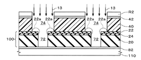
より具体的には、この配線構造体400は、デュアルダマシン法によって形成された導電層90を有する。より具体的には、この導電層90は、ビア層92と、ビア層92の上に連続して設けられた配線層94とを含む。ビア層92は、積層体100に設けられた第1の開口部72に埋め込まれており、配線層94は、有機系絶縁層40に設けられた第2の開口部74に埋め込まれている。なお、この配線層94は第1層目の配線層に限定されるわけではなく、第2層目以上の配線層であってもよい。また、ここでは、本発明の積層体が、ダマシン法によって形成される配線構造体の絶縁層として適用される例について示したが、本発明の積層体はダマシン法によって形成される配線構造体の絶縁層としてのみ適用されるわけではなく、半導体装置中のあらゆる絶縁層に適用可能である。
More specifically, the
積層体100は半導体基板110の上方に設けられ、有機系絶縁層40は積層体100の上に設けられている。より具体的には、半導体基板110上に拡散防止層82が設けられ、この半導体基板110が基体を構成し、拡散防止層82の上に積層体100が設けられている。また、第1の開口部72の底面において、拡散防止層82と導電層90とが接している。なお、図2に示すように、第1の開口部72および第2の開口部74の側面はバリア層80で覆われていてもよい。すなわち、この場合、積層体100とビア層92ならびに有機系絶縁層40と配線層94はバリア層80を介して隣り合っている。また、有機系絶縁層40の上にキャップ層42を設けることができる。
The
有機系絶縁層40としては、例えば、ポリアリーレン、ポリアリーレンエーテル、ポリイミド、ポリベンゾオキサゾール、ポリベンゾビスオキサゾール,ポリトリアゾール、ポリフェニルキノキサリン、ポリキノリン,ポリキノキサリンなどより選択される有機ポリマーが挙げられ、特にポリアリーレン、ポリアリーレンエーテルが好ましい。また、有機系絶縁層40として、上記有機ポリマーを1種あるいは2種以上組み合わせて用いることができる。
Examples of the organic insulating
この配線構造体400は例えば以下の方法により形成することができる。まず、半導体基板110の上方に拡散防止層82を形成した後、この拡散防止層82の上に積層体100を形成する(図3参照)。次に、積層体100上に有機系絶縁層40およびキャップ層42を順に形成する(図3参照)。次いで、キャップ層42、有機系絶縁層40および積層体100を貫通する開口部(スルーホール)70を形成する(図4参照)。具体的には、まず、キャップ層42上にレジスト層(図示せず)を成膜した後、一般的なフォトリソグラフィ工程によって、所定のパターンのレジスト層R1を形成する。このレジスト層R1は、後述する開口部70(図4参照)を形成するためのパターンを有する。次いで、このレジスト層R1をマスクとして、キャップ層42、有機系絶縁層40および積層体100をパターニングすることにより、開口部70を形成する(図4参照)。その後、アッシングなどによってレジスト層R1を除去する。なお、有機系絶縁層40が積層体100と同様に、塗布により形成される場合、一台の装置(スピンオンプロセス装置)のみで積層構造を形成することができるため、半導体製造時のスループット向上に大きく寄与する。
This
次いで、積層体100に第1の開口部72を、有機系絶縁層40に第2の開口部74をそれぞれ形成する(図5参照)。具体的には、まず、キャップ層42上にレジスト層(図示せず)を成膜した後、一般的なフォトリソグラフィ工程によって、所定のパターンのレジスト層R2を形成する。このレジスト層R2は、後述する第2の開口部74(図5参照)を形成するためのパターンを有する。次いで、このレジスト層R2をマスクとして、プラズマを用いたエッチングによりキャップ層42および有機系絶縁層40をパターニングして、第1の開口部72および第2の開口部74を形成する。その後、アッシングなどによりレジスト層R2を除去する。なお、まず有機系絶縁層40をパターニングして第2の開口部74を形成した後、積層体をパターニングして第1の開口部72を形成してもよい。
Next, the
キャップ層42および積層体100のエッチング方法としては、各種のプラズマを用いたエッチング方法(例えば、異方性プラズマエッチング、反応性プラズマエッチング,誘導結合型プラズマエッチング,ECRプラズマエッチング)などを用いることができる。また、有機系絶縁層40のエッチング方法およびレジスト層R1,R2のアッシング方法としては、酸素プラズマ処理、アンモニアプラズマ処理、水素/窒素混合ガスプラズマ処理、および窒素/酸素混合ガスを主成分とするドライエッチングプロセスが例示できる。
As an etching method of the
次に、例えばCVD法やスパッタリング法を用いて、第1の開口部72および第2の開口部74の表面にバリア層80を形成する(図6参照)。次いで、第1の開口部72および第2の開口部74に導電層90(図2参照)を形成する。具体的には、例えばPVD法にて銅シード層(図示せず)を形成した後、メッキ法によって第1の開口部72および第2の開口部74に導電性材料90aを埋め込む。次いで、CMPによりこの導電性材料90aを平坦化する。これにより、導電性材料90aのうちキャップ層42上に形成された部分が除去されて、導電層90が得られる(図2参照)。すなわち、第1の開口部72にはビア層92が形成され、第2の開口部74には配線層94が形成される。次いで、必要に応じて、導電層90およびキャップ層42の上にストッパ層32を形成する。以上の工程により、配線構造体400が得られる(図2参照)。
Next, the
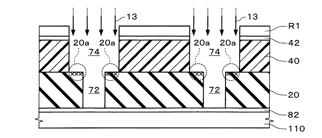
上述した工程においては、積層体100を貫通する第1の開口部72が設けられ、有機系絶縁層40に第2の開口部74が設けられる。この積層体100では、第1の層20上に第2の層22が設けられている。したがって、上述した工程のうちプラズマを用いたエッチングにて有機系絶縁層40をパターニングして第2の開口部74を形成する工程(図5参照)において、プラズマエッチングで生じる反応性イオン13を第2の層22が遮蔽することができる。これにより、第1の層20にダメージが生じるのを防止することができる。
In the process described above, the
これに対して、第1の層20上に第2の層22が形成されていない場合、図7に示すように、第1の層20がプラズマエッチングで生じる反応性イオン13に曝露され、特に第1の層20の露出面近傍20aにダメージが生じる。
On the other hand, when the
なお、本例では、プラズマを用いたエッチングにより有機系絶縁層40をパターニングする例について示したが、プラズマを用いたエッチングを行なう場合、有機系絶縁層40のかわりに無機系の絶縁層を用いても同様の課題が生じる。
In this example, an example in which the organic insulating
また、配線構造体400においては、第2の層22は第1の層20上に第3の層24を介して設けられている(図2参照)。このように、第1の層20と第2の層22との間に第3の層24が形成されていることにより、アルコキシシラン加水分解縮合物を含む塗布液を用いて第2の塗膜を形成し、この第2の塗膜を硬化させて第2の層22を形成する際に、第1の層20中の空孔へと前記アルコキシシラン加水分解縮合物が拡散するのを防止することができる。これにより、第2の層22の反応性イオンに対する遮蔽効果を確保することができるとともに、第1の層20のk値を設計値に維持することができる。
In the
[実施例]
次に、本発明を、実施例を挙げてさらに具体的に説明する。ただし、以下の記載は、本発明の態様を概括的に示すものであり、特に理由なく、かかる記載により本発明は限定されるものではない。また、実施例中における各評価は、次のようにして測定された。
[Example]
Next, the present invention will be described more specifically with reference to examples. However, the following description shows the aspect of this invention generally, and this invention is not limited by this description without a particular reason. Moreover, each evaluation in an Example was measured as follows.
(重量平均分子量(Mw))
下記条件によるゲルパーミエーションクロマトグラフィー(GPC)法により測定した。
(Weight average molecular weight (Mw))
It measured by the gel permeation chromatography (GPC) method by the following conditions.
試料:テトラヒドロフランを溶媒として使用し、加水分解縮合物1gを、100mlのテトラヒドロフランに溶解させて調製した。 Sample: Prepared by using tetrahydrofuran as a solvent and dissolving 1 g of hydrolysis condensate in 100 ml of tetrahydrofuran.
標準ポリスチレン:米国プレッシャーケミカル社製の標準ポリスチレンを使用した。 Standard polystyrene: Standard polystyrene manufactured by US Pressure Chemical Company was used.
装置:米国ウォーターズ社製の高温高速ゲル浸透クロマトグラム(モデル150−C ALC/GPC)
カラム:昭和電工(株)製のSHODEX A−80M(長さ50cm)
測定温度:40℃
流速:1cc/分
(比誘電率)
硬化膜が形成された基板上にアルミニウムを蒸着し、誘電率評価用基板を作製した。誘電率は、横川・ヒューレットパッカード(株)製のHP16451B電極およびHP4284AプレシジョンLCRメータを用いて、10kHzにおける容量値から算出した。
Apparatus: High-temperature high-speed gel permeation chromatogram (Model 150-C ALC / GPC) manufactured by Waters, USA
Column: SHODEX A-80M (length: 50 cm) manufactured by Showa Denko K.K.
Measurement temperature: 40 ° C
Flow rate: 1cc / min (dielectric constant)
Aluminum was vapor-deposited on the substrate on which the cured film was formed to produce a dielectric constant evaluation substrate. The dielectric constant was calculated from the capacitance value at 10 kHz using an HP16451B electrode and an HP4284A precision LCR meter manufactured by Yokogawa-Hewlett-Packard Co., Ltd.
(ハイライトエッチ法)
本実施例の積層体において、プラズマを用いた加工プロセス(プラズマCVD法)中の反応性イオンによる第1の層のダメージの評価は、ハイライトエッチ法を用いて行なった。すなわち、基板上に形成された積層体の第2の層上に、プラズマCVD法にて酸化珪素膜を積層後、この基板を劈開して得られた断面をフッ酸含有水溶液に所定時間浸漬した後、残存している第1の層の有無で判断する。
(Highlight etch method)
In the laminated body of this example, the damage evaluation of the first layer by reactive ions during the processing process using plasma (plasma CVD method) was performed using the highlight etching method. That is, after a silicon oxide film is laminated by the plasma CVD method on the second layer of the laminate formed on the substrate, the cross section obtained by cleaving this substrate is immersed in a hydrofluoric acid-containing aqueous solution for a predetermined time. Thereafter, the determination is made based on the presence or absence of the remaining first layer.
より具体的には、まず、積層体上に保護膜として炭素膜をスパッタ法にて50nm積層した。次いで、この保護膜が積層された積層体を8インチシリコン基板ごと短冊状に劈開し、ダイキン工業(株)製BHF-1100(フッ化アンモニウム2%水溶液)に25℃にて10,30,60秒浸漬した後、イオン交換水にて60秒洗浄し、その後大気下で乾燥した。次いで、走査型電子顕微鏡を用いて劈開面の形状を観察し、各時間における第1の層の残存の有無で以下の4段階に分類した。◎:60秒後残存、○:30秒後残存、△:10秒後残存、×:10秒後消失。 More specifically, first, a carbon film as a protective film was laminated on the laminate by 50 nm by a sputtering method. Next, the laminated body on which this protective film was laminated was cleaved into a strip shape together with the 8-inch silicon substrate, and 10, 30, 60 at 25 ° C. in BHF-1100 (2% aqueous solution of ammonium fluoride) manufactured by Daikin Industries, Ltd. After dipping for 2 seconds, it was washed with ion-exchanged water for 60 seconds, and then dried in the atmosphere. Next, the shape of the cleaved surface was observed using a scanning electron microscope, and was classified into the following four stages depending on whether or not the first layer remained at each time. A: Remaining after 60 seconds, B: Remaining after 30 seconds, Δ: Remaining after 10 seconds, X: Disappearing after 10 seconds.
(1)塗布液1の作製
石英製セパラブルフラスコに、エタノール570g、イオン交換水160gおよび10%水酸化テトラメチルアンモニウム水溶液30gを入れ、均一に攪拌した。この溶液にメチルトリメトキシシラン136gとテトラエトキシシラン209gの混合物を添加した。溶液を60℃に保ったまま、5時間反応を行った。この溶液にプロピレングリコールモノプロピルエーテル300gを加え、その後、50℃のエバポレータを用いて溶液を10%(完全加水分解縮合物換算)となるまで濃縮し、その後、酢酸の10%プロピレングリコールモノプロピルエーテル溶液を添加し、濃度3%(完全加水分解縮合物換算)の反応液1を得た。この溶液を0.2μm孔径のテフロン(登録商標)製フィルターでろ過を行い塗布液1を得た。
(1) Preparation of coating solution 1 In a quartz separable flask, 570 g of ethanol, 160 g of ion-exchanged water, and 30 g of 10% tetramethylammonium hydroxide aqueous solution were added and stirred uniformly. To this solution, a mixture of 136 g of methyltrimethoxysilane and 209 g of tetraethoxysilane was added. The reaction was carried out for 5 hours while keeping the solution at 60 ° C. To this solution was added 300 g of propylene glycol monopropyl ether, and then the solution was concentrated to 10% (in terms of complete hydrolysis condensate) using an evaporator at 50 ° C., and then 10% propylene glycol monopropyl ether of acetic acid. The solution was added to obtain a reaction solution 1 having a concentration of 3% (in terms of complete hydrolysis condensate). This solution was filtered through a Teflon (registered trademark) filter having a pore size of 0.2 μm to obtain a coating solution 1.
このようにして得られた縮合物等の重量平均分子量は、60,000であった。また、8インチシリコン基板上に塗布液1をスピンコート法で塗布し、80℃で1分間、200℃で1分間乾燥後、さらに真空下400℃で30分間加熱することにより硬化膜1(第1の層)を得た。この硬化膜1の比誘電率は2.23であった。 The weight average molecular weight of the condensate obtained in this manner was 60,000. Also, the coating liquid 1 is applied onto an 8-inch silicon substrate by spin coating, dried at 80 ° C. for 1 minute, 200 ° C. for 1 minute, and further heated at 400 ° C. for 30 minutes under vacuum to obtain a cured film 1 (first film). 1 layer). The relative dielectric constant of the cured film 1 was 2.23.
(2)塗布液2の作製
石英製セパラブルフラスコ中で、メチルトリメトキシシラン243.30g、テトラメトキシシラン101.24g、トリエトキシシラン123.64gとテトラキス(アセチルアセトナート)チタン0.02gを、ジプロピレングリコールジメチルエーテル254gに溶解させた後、均一に攪拌させ、溶液温度を50℃に安定させた。次に、イオン交換水278gを1時間かけて溶液に添加した。その後、50℃で3時間反応させた後、ジプロピレングリコールジメチルエーテル546gを加え反応液を室温まで冷却した後、50℃のエバポレーターを用いて、溶液を20%(完全加水分解縮合物換算)となるまで濃縮し、その後、プロピレングリコールモノプロピルエーテルを添加し、濃度0.5%(完全加水分解縮合物換算)の反応液2を得た。この溶液を0.2μm孔径のテフロン(登録商標)製フィルターでろ過を行い塗布液2を得た。
(2) Preparation of
また、塗布液2を用いて上述の硬化膜1を形成する方法と同様の方法にて硬化膜2(第2の層)を作製した。このようにして得られた縮合物等の重量平均分子量は、7,600であり、硬化膜2の比誘電率は2.77であった。
Moreover, the cured film 2 (2nd layer) was produced by the method similar to the method of forming the above-mentioned cured film 1 using the
(3)塗布液3の作製
石英製セパラブルフラスコに、メタノール500g、イオン交換水228gおよび20%メチルアミン水溶液6.0gを入れ、55℃で撹拌を行った。この溶液にメチルトリエトキシシラン21.5gとテトラエトキシシラン26.7gの混合物を一定速度で1時間かけて添加した。この溶液を55℃でさらに1時間反応させた後、下記構造式(1)で表される繰り返し単位を有する重量分子量5,000のポリシロキサン79.5gを30分かけて添加した。
(3) Preparation of Coating Solution 3 500 g of methanol, 228 g of ion-exchanged water, and 6.0 g of a 20% aqueous methylamine solution were placed in a quartz separable flask and stirred at 55 ° C. A mixture of 21.5 g of methyltriethoxysilane and 26.7 g of tetraethoxysilane was added to this solution at a constant rate over 1 hour. After this solution was further reacted at 55 ° C. for 1 hour, 79.5 g of a polysiloxane having a weight molecular weight of 5,000 having a repeating unit represented by the following structural formula (1) was added over 30 minutes.
この溶液を55℃でさらに3時間反応させた。次いで、この溶液に20%マレイン酸水溶液56gとプロピレングリコールモノプロピルエーテル440gを加え、その後、50℃のエバポレーターを用いて溶液を20%(完全加水分解縮合物換算)となるまで濃縮し、その後、プロピレングリコールモノプロピルエーテルを添加し、濃度0.5%(完全加水分解縮合物換算)の反応液3を得た。この反応液3を0.2μm孔径のテフロン(登録商標)フィルターでろ過を行い塗布液3を得た。 This solution was further reacted at 55 ° C. for 3 hours. Next, 56 g of a 20% maleic acid aqueous solution and 440 g of propylene glycol monopropyl ether are added to this solution, and then the solution is concentrated to 20% (in terms of complete hydrolysis condensate) using an evaporator at 50 ° C., and then Propylene glycol monopropyl ether was added to obtain a reaction solution 3 having a concentration of 0.5% (in terms of complete hydrolysis condensate). The reaction solution 3 was filtered through a Teflon (registered trademark) filter having a pore size of 0.2 μm to obtain a coating solution 3.
また、塗布液3を用いて上述の硬化膜1を形成する方法と同様の方法にて硬化膜3(第3の層)を作製した。このようにして得られた縮合物等の重量平均分子量は、20,000であり、硬化膜3の比誘電率は2.67であった。 Moreover, the cured film 3 (third layer) was produced by the same method as the method of forming the cured film 1 described above using the coating liquid 3. The weight average molecular weight of the condensate thus obtained was 20,000, and the relative dielectric constant of the cured film 3 was 2.67.
(4)積層体1の作製
8インチシリコン基板上に、上記(1)で製造した塗布液1をスピンコート法で塗布し、80℃で1分間、200℃で1分間乾燥し、未硬化の第1の塗膜を形成した。さらに、この上に、上記(2)で製造した塗布液2をスピンコート法により塗布し、大気中90℃で1分間、次いで窒素下200℃で1分間加熱し、さらに真空下400℃で30分加熱することにより、第1の塗膜(膜厚100nm)上に第2の塗膜(膜厚10nm)を積層した。さらにこの上に、膜厚100nmの酸化珪素膜をプラズマCVD法により形成し、第1の層および第2の層からなる積層体1を得た。
(4) Production of Laminate 1 On an 8-inch silicon substrate, the coating solution 1 produced in (1) above is applied by spin coating, dried at 80 ° C. for 1 minute, and 200 ° C. for 1 minute, and uncured. A first coating was formed. Further thereon, the
積層体1中の第1の層におけるプラズマダメージ(プラズマCVD工程における反応性イオンによるダメージ)を、ハイライトエッチ法を用いて評価したところ、○であった。 The plasma damage (damage caused by reactive ions in the plasma CVD process) in the first layer in the laminate 1 was evaluated by using the highlight etch method, and was evaluated as ◯.
8インチシリコン基板上に、上記実施例1の(1)で製造した塗布液1をスピンコート法で塗布し、80℃で1分間、200℃で1分間乾燥し、膜厚100nmの未硬化の第1の塗膜を形成した。続いて、この上に、上記実施例1の(3)で製造した塗布液3をスピンコート法により塗布し、大気中90℃で1分間、次いで窒素下200℃で1分間加熱し、膜厚10nmの未硬化の第3の塗膜を形成した。さらに、この上に、上記実施例1の(2)で製造した塗布液2をスピンコート法により塗布した。これにより、第1の塗膜(膜厚100nm)上に第3の塗膜(膜厚10nm)および第2の塗膜(膜厚10nm)が順に積層された。次いで、この積層体を大気中90℃で1分間、次いで窒素下200℃で1分間加熱し、さらに真空下400℃で30分加熱することにより、第1の層上に第3の層および第2の層が順に積層された積層体300が得られた。さらにこの上に膜厚100nmの酸化珪素層をプラズマCVD法により形成した。この積層体2の構成を図8に示す。この積層体2では、第1の層20と第2の層22との間に第3の層24が形成されている。また、積層体2上に酸化珪素層60が形成されている。
On an 8-inch silicon substrate, the coating solution 1 produced in (1) of Example 1 was applied by spin coating, dried at 80 ° C. for 1 minute, and 200 ° C. for 1 minute, and an uncured film having a thickness of 100 nm. A first coating was formed. Subsequently, the coating solution 3 produced in (3) of Example 1 was applied thereon by a spin coating method, heated in the atmosphere at 90 ° C. for 1 minute, and then heated at 200 ° C. for 1 minute in nitrogen to form a film thickness. A 10 nm uncured third coating was formed. Further thereon, the
積層体2中の第1の層20におけるプラズマダメージを、ハイライトエッチ法を用いて評価したところ、◎であった。
When the plasma damage in the
(比較例)
8インチシリコン基板上に、上記実施例1の(1)で製造した塗布液1をスピンコート法で塗布し、80℃で1分間、次いで200℃で1分間乾燥し、未硬化の第1の塗膜を形成した。続いて、真空下400℃で30分間加熱することにより第1の塗膜(膜厚100nm)を得た。この上に、膜厚100nmの酸化珪素層をプラズマCVD法により形成し、第1の層からなる積層体3を得た。
(Comparative example)
The coating liquid 1 produced in (1) of Example 1 above was applied onto an 8-inch silicon substrate by spin coating, dried at 80 ° C. for 1 minute, and then at 200 ° C. for 1 minute. A coating film was formed. Then, the 1st coating film (film thickness of 100 nm) was obtained by heating at 400 degreeC for 30 minutes under vacuum. On top of this, a silicon oxide layer having a thickness of 100 nm was formed by a plasma CVD method to obtain a laminate 3 composed of the first layer.
積層体3中の第1の層におけるプラズマダメージを、ハイライトエッチ法を用いて評価したところ、×であった。 It was x when the plasma damage in the 1st layer in the laminated body 3 was evaluated using the highlight etching method.
以上に示したように、実施例1、2および比較例によれば、第1の層上に第2の層が形成されていることにより、プラズマ処理(プラズマCVD法)の際に第1の層に加わるダメージを低減できたことが確認された。 As described above, according to the first and second embodiments and the comparative example, the second layer is formed on the first layer, so that the first process is performed during the plasma processing (plasma CVD method). It was confirmed that the damage applied to the layer could be reduced.
2,100 積層体
10 基体
13 反応性イオン
20 第1の層
20a 第1の層の露出面近傍
22 第2の層
22a 第2の層の露出面近傍
24 第3の層
32 ストッパ層
40 有機系絶縁層
42 キャップ層
60 酸化珪素層
70 開口部
72 第1の開口部
74 第2の開口部
80 バリア層
82 拡散防止層
90 導電層
90a 導電性材料
92 ビア層
94 配線層
110 半導体基板
400 配線構造体
R1,R2 レジスト層
2,100
Claims (2)
(b)アルコキシシラン加水分解縮合物を含む塗布液を塗布して第3の塗膜を形成し、および
(c)前記第3の塗膜の上方に、前記アルコキシシラン加水分解縮合物を含む塗布液を塗布して第2の塗膜を形成した後、前記第1、第2および第3の塗膜を加熱硬化することにより、比誘電率が2.5以下である第1の層と、比誘電率が2.5を超える第2の層と、前記第1の層と前記第2の層との間に、Siを含有し、かつO、C、N、Hの群から選ばれる少なくとも1種の元素を含有する第3の層とを含む積層体を形成すること、
を含む、積層体の形成方法。 (A) A coating solution containing an alkoxysilane hydrolysis condensate is applied onto a substrate and dried to form a first coating film;
(B) applying a coating solution containing an alkoxysilane hydrolysis condensate to form a third coating film; and (c) an application containing the alkoxysilane hydrolysis condensate above the third coating film. After the liquid is applied to form the second coating film, the first, second, and third coating films are heated and cured, whereby the first layer having a relative dielectric constant of 2.5 or less, A second layer having a relative dielectric constant exceeding 2.5, and between the first layer and the second layer, containing Si and at least selected from the group of O, C, N, and H Forming a laminate including a third layer containing one element;
A method for forming a laminate including:
(b)アルコキシシラン加水分解縮合物を含む塗布液を塗布して第3の塗膜を形成し、および
(c)前記第3の塗膜の上方に、アルコキシシラン加水分解縮合物を含む塗布液を塗布して第2の塗膜を形成した後、前記第1、第2および第3の塗膜を電子線もしくは紫外線硬化することにより、比誘電率が2.5以下である第1の層と、比誘電率が2.5を超える第2の層と、前記第1の層と前記第2の層との間に、Siを含有し、かつO、C、N、Hの群から選ばれる少なくとも1種の元素を含有する第3の層とを含む積層体を形成すること、を含む、積層体の形成方法。 (A) A coating solution containing an alkoxysilane hydrolysis condensate is applied onto a substrate and dried to form a first coating film;
(B) A coating liquid containing an alkoxysilane hydrolysis condensate is applied to form a third coating film, and (c) a coating liquid containing an alkoxysilane hydrolysis condensate above the third coating film. Is applied to form a second coating film, and then the first, second, and third coating films are cured with an electron beam or an ultraviolet ray so that the first dielectric layer has a relative dielectric constant of 2.5 or less. And a second layer having a relative dielectric constant exceeding 2.5, and containing Si between the first layer and the second layer, and selected from the group of O, C, N, and H Forming a laminated body including a third layer containing at least one kind of element.
Priority Applications (1)
| Application Number | Priority Date | Filing Date | Title |
|---|---|---|---|
| JP2003351843A JP4150922B2 (en) | 2003-10-10 | 2003-10-10 | Method for forming laminate |
Applications Claiming Priority (1)
| Application Number | Priority Date | Filing Date | Title |
|---|---|---|---|
| JP2003351843A JP4150922B2 (en) | 2003-10-10 | 2003-10-10 | Method for forming laminate |
Publications (2)
| Publication Number | Publication Date |
|---|---|
| JP2005116925A JP2005116925A (en) | 2005-04-28 |
| JP4150922B2 true JP4150922B2 (en) | 2008-09-17 |
Family
ID=34542965
Family Applications (1)
| Application Number | Title | Priority Date | Filing Date |
|---|---|---|---|
| JP2003351843A Expired - Fee Related JP4150922B2 (en) | 2003-10-10 | 2003-10-10 | Method for forming laminate |
Country Status (1)
| Country | Link |
|---|---|
| JP (1) | JP4150922B2 (en) |
Families Citing this family (4)
| Publication number | Priority date | Publication date | Assignee | Title |
|---|---|---|---|---|
| KR101271437B1 (en) | 2005-05-31 | 2013-06-05 | 미쓰비시 가가꾸 폴리에스테르 필름 가부시키가이샤 | Mold release film |
| JP4916132B2 (en) * | 2005-05-31 | 2012-04-11 | 三菱樹脂株式会社 | Release film |
| JP4916131B2 (en) * | 2005-05-31 | 2012-04-11 | 三菱樹脂株式会社 | Release film |
| JP4716035B2 (en) * | 2007-02-14 | 2011-07-06 | Jsr株式会社 | Silica-based film and method for forming the same |
-
2003
- 2003-10-10 JP JP2003351843A patent/JP4150922B2/en not_active Expired - Fee Related
Also Published As
| Publication number | Publication date |
|---|---|
| JP2005116925A (en) | 2005-04-28 |
Similar Documents
| Publication | Publication Date | Title |
|---|---|---|
| KR100822138B1 (en) | Method for Forming Dual Damascene Structure | |
| EP1296365B1 (en) | Method of film formation | |
| US20060275614A1 (en) | Insulating film and method for forming the same, and film-forming composition | |
| WO2005082976A1 (en) | Polymer and process for producing the same, composition for forming insulating film, and insulating film and method of forming the same | |
| WO2005108469A1 (en) | Method for forming organic silica film, organic silica film, wiring structure, semiconductor device, and composition for film formation | |
| JPWO2005108469A1 (en) | Method for forming organic silica film, organic silica film, wiring structure, semiconductor device, and film forming composition | |
| JP5099302B2 (en) | Composition for forming insulating film, polymer and method for producing the same, method for producing insulating film, and silica-based insulating film | |
| JP2004059737A (en) | Method for producing polysiloxane for film formation, composition for film formation, method for film formation, and film | |
| JP4849219B2 (en) | Surface hydrophobizing composition, surface hydrophobizing method, and semiconductor device | |
| JP2007035705A (en) | Surface hydrophobing method, surface hydrophobing composite, and semiconductor device and its manufacturing method | |
| JP4150922B2 (en) | Method for forming laminate | |
| JP2005093688A (en) | Semiconductor device and manufacturing method therefor | |
| JP4344893B2 (en) | Method for producing composition for forming interlayer insulating film | |
| JP2005179587A (en) | Composition for use in membrane formation, forming method for membrane, and silica-based membrane | |
| JP4780277B2 (en) | Surface hydrophobizing composition, surface hydrophobizing method, semiconductor device and manufacturing method thereof | |
| JP4883256B2 (en) | Surface hydrophobizing composition, surface hydrophobizing method, semiconductor device and manufacturing method thereof | |
| JP4101989B2 (en) | Method for producing polyorganosiloxane composition, polyorganosiloxane composition, and film | |
| JP4513249B2 (en) | Manufacturing method of copper damascene structure | |
| JP2006114719A (en) | Composition for surface hydrophobing, method of hydrophobing surface, semiconductor device and its manufacturing method | |
| JP2006198552A (en) | Method for making surface hydrophobic, and semiconductor device and its manufacturing method | |
| JP5184737B2 (en) | Surface hydrophobizing composition, surface hydrophobizing method, semiconductor device and manufacturing method thereof | |
| JP2006111738A (en) | Composition for surface hydrophobizing, surface hydrophobizing method, semiconductor device and its manufacturing method | |
| JP4411687B2 (en) | Method for producing film forming composition, film forming composition and insulating film forming material | |
| JP4798334B2 (en) | Surface hydrophobizing composition, surface hydrophobizing method, semiconductor device and manufacturing method thereof | |
| JP4780276B2 (en) | Surface hydrophobization method and semiconductor device manufacturing method |
Legal Events
| Date | Code | Title | Description |
|---|---|---|---|
| A621 | Written request for application examination |
Free format text: JAPANESE INTERMEDIATE CODE: A621 Effective date: 20051104 |
|
| A977 | Report on retrieval |
Free format text: JAPANESE INTERMEDIATE CODE: A971007 Effective date: 20071129 |
|
| A131 | Notification of reasons for refusal |
Free format text: JAPANESE INTERMEDIATE CODE: A131 Effective date: 20080319 |
|
| A521 | Request for written amendment filed |
Free format text: JAPANESE INTERMEDIATE CODE: A523 Effective date: 20080512 |
|
| TRDD | Decision of grant or rejection written | ||
| A01 | Written decision to grant a patent or to grant a registration (utility model) |
Free format text: JAPANESE INTERMEDIATE CODE: A01 Effective date: 20080604 |
|
| A01 | Written decision to grant a patent or to grant a registration (utility model) |
Free format text: JAPANESE INTERMEDIATE CODE: A01 |
|
| A61 | First payment of annual fees (during grant procedure) |
Free format text: JAPANESE INTERMEDIATE CODE: A61 Effective date: 20080617 |
|
| R150 | Certificate of patent or registration of utility model |
Free format text: JAPANESE INTERMEDIATE CODE: R150 Ref document number: 4150922 Country of ref document: JP Free format text: JAPANESE INTERMEDIATE CODE: R150 |
|
| FPAY | Renewal fee payment (event date is renewal date of database) |
Free format text: PAYMENT UNTIL: 20110711 Year of fee payment: 3 |
|
| FPAY | Renewal fee payment (event date is renewal date of database) |
Free format text: PAYMENT UNTIL: 20110711 Year of fee payment: 3 |
|
| FPAY | Renewal fee payment (event date is renewal date of database) |
Free format text: PAYMENT UNTIL: 20110711 Year of fee payment: 3 |
|
| FPAY | Renewal fee payment (event date is renewal date of database) |
Free format text: PAYMENT UNTIL: 20110711 Year of fee payment: 3 |
|
| FPAY | Renewal fee payment (event date is renewal date of database) |
Free format text: PAYMENT UNTIL: 20120711 Year of fee payment: 4 |
|
| R250 | Receipt of annual fees |
Free format text: JAPANESE INTERMEDIATE CODE: R250 |
|
| FPAY | Renewal fee payment (event date is renewal date of database) |
Free format text: PAYMENT UNTIL: 20120711 Year of fee payment: 4 |
|
| FPAY | Renewal fee payment (event date is renewal date of database) |
Free format text: PAYMENT UNTIL: 20120711 Year of fee payment: 4 |
|
| FPAY | Renewal fee payment (event date is renewal date of database) |
Free format text: PAYMENT UNTIL: 20130711 Year of fee payment: 5 |
|
| R250 | Receipt of annual fees |
Free format text: JAPANESE INTERMEDIATE CODE: R250 |
|
| R250 | Receipt of annual fees |
Free format text: JAPANESE INTERMEDIATE CODE: R250 |
|
| R250 | Receipt of annual fees |
Free format text: JAPANESE INTERMEDIATE CODE: R250 |
|
| R250 | Receipt of annual fees |
Free format text: JAPANESE INTERMEDIATE CODE: R250 |
|
| R250 | Receipt of annual fees |
Free format text: JAPANESE INTERMEDIATE CODE: R250 |
|
| R250 | Receipt of annual fees |
Free format text: JAPANESE INTERMEDIATE CODE: R250 |
|
| R250 | Receipt of annual fees |
Free format text: JAPANESE INTERMEDIATE CODE: R250 |
|
| R250 | Receipt of annual fees |
Free format text: JAPANESE INTERMEDIATE CODE: R250 |
|
| R250 | Receipt of annual fees |
Free format text: JAPANESE INTERMEDIATE CODE: R250 |
|
| LAPS | Cancellation because of no payment of annual fees |