JP4149151B2 - I / O buffer circuit - Google Patents
I / O buffer circuit Download PDFInfo
- Publication number
- JP4149151B2 JP4149151B2 JP2001258877A JP2001258877A JP4149151B2 JP 4149151 B2 JP4149151 B2 JP 4149151B2 JP 2001258877 A JP2001258877 A JP 2001258877A JP 2001258877 A JP2001258877 A JP 2001258877A JP 4149151 B2 JP4149151 B2 JP 4149151B2
- Authority
- JP
- Japan
- Prior art keywords
- voltage
- pmos transistor
- power supply
- input
- supply voltage
- Prior art date
- Legal status (The legal status is an assumption and is not a legal conclusion. Google has not performed a legal analysis and makes no representation as to the accuracy of the status listed.)
- Expired - Fee Related
Links
Images


Landscapes
- Logic Circuits (AREA)
Description
【0001】
【発明の属する技術分野】
本発明は、入出力バッファ回路に関するものであり、特に、自己の電源電圧に比して高い電圧レベルの電圧信号が、入出力端子に直接入力されるPMOSトランジスタを含む入出力バッファ回路に関するものである。
【0002】
【従来の技術】
入出力バッファ回路とは、半導体集積回路(以下、LSIと称する)の外部に信号を出力し、また外部から信号を入力する、信号を双方向に伝播することのできるバッファ回路である。1例として、図9に入出力バッファ回路1を示す。LSIの外部との接続部分である入出力端子PADから入力された信号は、入出力バッファ部B内の入力バッファ部BIに入力される。この時出力バッファ部BOは出力イネーブル信号(不図示)により非活性となっている。信号の出力は、出力イネーブル信号により活性化された出力バッファ部BOより、入出力端子PADから行われる。ここで、出力バッファ部BOは、CMOS構成のドライブ段を有しているものとし、図9においては、このうちPMOSトランジスタBM1が例示されている。
【0003】
また、図9では、入出力バッファ回路1は、入出力バッファ部B以外に、外部入出力端子PADからの静電気等のサージ電圧による内部素子の静電破壊を防止するための静電破壊保護部D、入力モード時に高電圧側の入力電圧レベルを所定電圧レベルにクランプするクランプ部Cを備えている。
【0004】
静電破壊保護部Dは、入出力端子PADから入力されるサージ電圧を、電源電圧VDD1及び接地電圧GNDに吸収するためのダイオード素子DU、DLで構成されている。これらのダイオード素子DU、DLは、PN接合で構成できるほか、ダイオード接続されたMOSトランジスタで構成することもできる。例えば、ダイオード素子DUを、PMOSトランジスタで構成するには、ソース端子、ゲート端子、及びバックゲート端子を電源電圧VDD1に接続し、ドレイン端子を入出力端子PADに接続して構成する。入出力端子PADに、電源電圧VDD1から、ダイオード接続されたPMOSトランジスタの閾値電圧を加えた電圧以上のサージ電圧が印加された際、PMOSトランジスタで構成されたダイオード素子DUが導通し、サージ電圧を電源電圧VDD1側に逃がす経路が形成されることにより、入出力バッファ部B等の内部回路をサージ電圧から保護する働きを有している。
【0005】
クランプ部Cは、入出力端子PADがフローティング状態の際に、電圧レベルをクランプするための回路である。プルアップ制御回路C1により制御されたPMOSトランジスタCM1が、必要に応じて導通することにより、入出力端子PADを電源電圧VDD1にクランプする。
【0006】
近年のLSIの微細化等の進展により、LSIの駆動電源電圧は低下してきており、個々に異なる電源電圧で動作するLSIを複数組み合わせてシステムを構成する場合がある。このとき、異種電源電圧で動作するLSIの入出力端子同士を直接接続できれば好都合であり、これを実現するための提案が従来よりなされている。この提案は、PMOSトランジスタのNウェル電位を、電源電圧と入力される電圧信号とのうち高電圧側でバイアスするNウェル電位制御部Aを備えるというものであり、具体的には以下の方法がある。
【0007】
図10に示すNウェル電位制御部A100は、ソース端子を電源電圧VDD1に接続し、ドレイン端子及びバックゲート端子をNウェルNWに接続し、更にゲート端子を入出力端子PAD(入出力される電圧信号VIN)に接続する第1PMOSトランジスタPM1と、ソース端子を入出力端子PADに接続し、ドレイン端子及びバックゲート端子をNウェルNWに接続し、更にゲート端子を電源電圧VDD1に接続する第2PMOSトランジスタPM2とにより構成されている。
【0008】
PMOSトランジスタPM1、PM2の閾値電圧をVthPとすると、VIN<VDD1−VthPの場合には、第1PMOSトランジスタPM1のゲート端子に印加される電圧信号VINが、ソース端子に印加される電源電圧VDD1に比して低く、しかもその電位差が、閾値電圧VthP以上となっている。従って、第1PMOSトランジスタPM1は線形動作をして導通し、NウェルNWと電源電圧VDD1が接続される。一方、第2PMOSトランジスタPM2においては、ゲート端子とソース端子との電圧関係が、第1PMOSトランジスタPM1とは反対の関係となるので、非導通状態を維持している。よって、NウェルNWの電位VNWは、電源電圧VDD1にバイアスされる。
【0009】
VIN>VDD1+VthPの場合には、第1及び第2PMOSトランジスタPM1、PM2のゲート端子とソース端子との電圧関係が、上記とは逆の関係となる。即ち、第1PMOSトランジスタPM1は非導通状態になる一方で、第2PMOSトランジスタPM2が線形動作をして導通することとなる。従って、NウェルNWの電位VNWは、電圧信号VINにバイアスされる。
【0010】
図10のNウェル電位制御部A100では、NウェルNWは、VIN<VDD1−VthPの場合には、電源電圧VDD1にバイアスされ、VIN>VDD1+VthPの場合には、電圧信号VINにバイアスされる。これらの領域では、NウェルNWは、電源電圧VDD1と電圧信号VINのうち高い電圧側にバイアスされる。
【0011】
【発明が解決しようとする課題】
しかしながら、Nウェル電位制御部A100においては、VDD1−VthP<VIN<VDD1+VthPの領域において、NウェルNWがフローティング状態となり問題である。
【0012】
以上のように、NウェルNWの電位VNWが、フローティング状態にあると、図9における出力バッファ部BOのドライブ段PMOSトランジスタBM1、クランプ部CのPMOSトランジスタCM1、及び静電破壊保護部DのPMOSトランジスタで構成されたダイオード素子DU等のPMOSトランジスタにおけるバックゲートバイアスが不安定となり、バックゲートバイアス効果による閾値電圧の不安定化に伴う駆動能力の不安定化、スイッチン制御の不安定化、あるいはドレイン端子からNウェルNWへのPN接合における順方向電流の増大等、回路動作上の種々の不具合が発生する虞があり問題である。
【0013】
本発明は前記従来技術の問題点を解消するためになされたものであり、PMOSトランジスタを含む入出力バッファ回路において、自己の電源電圧とは異なる電圧の電圧信号が入出力端子に直接入力されても、Nウェル電位を確実にバイアスすることができ、電圧信号の全ての電圧範囲において、Nウェル電位がフローティング状態にならないNウェル電位制御部を備えた入出力バッファ回路を提供することを目的とする。
【0014】
【課題を解決するための手段】
前記目的を達成するために、請求項1に係る入出力バッファ回路は、自己の電源電圧に比して高い電圧レベルの電圧信号が、入出力端子に直接入力される入出力バッファ回路において、電圧信号がドレイン端子に印加されるPMOSトランジスタのNウェル電位を、電圧信号が、電源電圧に比して第1所定電圧値以下の電圧となる第1領域では電源電圧に、電圧信号が、電源電圧に比して第2所定電圧値以上の電圧となる第2領域では電圧信号に、電圧信号が、第1及び第2領域に挟まれた電圧となる第3領域では電源電圧、あるいは電圧信号に設定するNウェル電位制御部を備え、Nウェル電位制御部は、ソース端子が電源電圧に接続され、ドレイン端子及びバックゲート端子がNウェルに接続される第1PMOSトランジスタと、ソース端子が入出力端子に接続され、ドレイン端子及びバックゲート端子がNウェルに接続され、更にゲート端子が電源電圧に接続される第2PMOSトランジスタと、第2所定電圧値を、第2PMOSトランジスタの閾値電圧値とし、第1及び第3領域において、第1PMOSトランジスタを導通し、第2領域において、第1PMOSトランジスタを非導通にするPMOSトランジスタ制御部とを備えることを特徴とする。
【0015】
請求項1の入出力バッファ回路では、Nウェル電位制御部により、電圧信号がドレイン端子に印加されるPMOSトランジスタのNウェル電位を、入出力端子の電圧信号の電圧レベルに応じて、電源電圧と電圧信号との間で適宜切り替える。切り換える電圧信号の電圧レベルは、電源電圧との大小関係に応じて行われる。即ち、電圧信号が、電源電圧に比して第1所定電圧値以下の電圧となる第1領域では電源電圧に設定し、電源電圧に比して第2所定電圧値以上の電圧となる第2領域では電圧信号に設定する。そして、中間の第3領域では何れは一方の電圧レベルに設定される。この場合、第2PMOSトランジスタのソース端子が入出力端子に接続され、ゲート端子が電源電圧に接続されているため、電圧信号の電圧レベルが、電源電圧に第2PMOSトランジスタの閾値電圧を加えた電圧以上に昇圧した場合に、第2PMOSトランジスタは導通してNウェルに電圧信号を供給する。一方、第1PMOSトランジスタは、PMOSトランジスタ制御部によって制御される。電圧信号の電圧レベルが、電源電圧に第2PMOSトランジスタの閾値電圧を加えた電圧を閾値電圧として、この電圧以下の第1及び第3領域では導通してNウェルに電源電圧を供給すると共に、この電圧以上の第2領域では非導通となる。通常、第1及び第2PMOSトランジスタの閾値電圧は一致する。従って、第1及び第3領域では、第2PMOSトランジスタが非導通になると共に第1PMOSトランジスタが導通してNウェル電位を電源電圧にし、第2領域では、第1PMOSトランジスタが非導通になると共に第2PMOSトランジスタが導通してNウェル電位を電圧信号にする。
また、請求項4に係る入出力バッファ回路は、自己の電源電圧に比して高い電圧レベルの電圧信号が、入出力端子に直接入力される入出力バッファ回路において、電圧信号がドレイン端子に印加されるPMOSトランジスタのNウェル電位を、電圧信号が、電源電圧に比して第1所定電圧値以下の電圧となる第1領域では前記電源電圧に、電圧信号が、電源電圧に比して第2所定電圧値以上の電圧となる第2領域では前記電圧信号に、電圧信号が、第1及び第2領域に挟まれた電圧となる第3領域では電源電圧、あるいは電圧信号に設定するNウェル電位制御部を備え、Nウェル電位制御部は、第1及び第2PMOSトランジスタとを備えており、各々のソース端子、ドレイン端子、及びバックゲート端子については、請求項1と同様な接続関係を有しながら、第1PMOSトランジスタのゲート端子が入出力端子に接続されている。第2PMOSトランジスタは、第1所定電圧値を、第1PMOSトランジスタの閾値電圧値とし、第1領域において、第2PMOSトランジスタを非導通とし、第2及び第3領域において、第2PMOSトランジスタを導通するPMOSトランジスタ制御部を備えることを特徴とする。
請求項4の入出力バッファ回路では、Nウェル電位制御部により、電圧信号がドレイン 端子に印加されるPMOSトランジスタのNウェル電位を、入出力端子の電圧信号の電圧レベルに応じて、電源電圧と電圧信号との間で適宜切り替える。切り換える電圧信号の電圧レベルは、電源電圧との大小関係に応じて行われる。即ち、電圧信号が、電源電圧に比して第1所定電圧値以下の電圧となる第1領域では電源電圧に設定し、電源電圧に比して第2所定電圧値以上の電圧となる第2領域では電圧信号に設定する。そして、中間の第3領域では何れは一方の電圧レベルに設定される。この場合、第1及び第2PMOSトランジスタのゲート端子への接続が、請求項1における接続と反対の関係を有している。第1PMOSトランジスタは、電圧信号の電圧レベルが、電源電圧より第1PMOSトランジスタの閾値電圧以下に降圧した場合に導通して、Nウェルに電源電圧を供給する。一方、第2PMOSトランジスタは、PMOSトランジスタ制御部に制御される。電圧信号の電圧レベルが、電源電圧より第1PMOSトランジスタの閾値電圧を下回った電圧を閾値電圧として、この電圧以下の第1領域では非導通となると共に、この電圧以上の第2及び第3領域では導通してNウェルに電圧信号を供給する。通常、第1及び第2PMOSトランジスタの閾値電圧は一致するので、第1領域では、第1PMOSトランジスタが導通すると共に第2PMOSトランジスタが非導通となってNウェル電位を電源電圧にし、第2及び第3領域では、第1PMOSトランジスタが非導通になると共に第2PMOSトランジスタが導通してNウェル電位を電圧信号にする。
【0016】
これにより、PMOSトランジスタのNウェル電位は、入出力端子に印加される電圧信号の電圧レベルに応じて適宜な電圧が設定されるので、所定電圧レベルにおいて、フローティング状態となることはない。従って、入出力端子の電圧信号におけるあらゆる電圧レベルに対して、Nウェル電位を確実に設定することができ、入出力バッファ回路において、入力状態、出力状態を問わず、常に安定した回路動作を得ることができる。
PMOSトランジスタの閾値電圧を利用して、電源電圧から閾値電圧離れた電圧信号の電圧レベルを境界として、Nウェル電位を電源電圧と電圧信号との間で切り替えることができる。
【0017】
また、請求項2に係る入出力バッファ回路は、請求項1に記載の入出力バッファ回路において、Nウェル電位制御部は、第3領域では、Nウェル電位を前記電源電圧に固定するNウェル電位制御部である。
【0018】
【0019】
【0020】
【0021】
【0022】
【0023】
また、請求項3に係る入出力バッファ回路は、請求項1または2に記載の入出力バッファ回路において、PMOSトランジスタ制御部は、ソース端子が第1PMOSトランジスタのゲート端子に、ドレイン端子が入出力端子に接続され、ゲート端子に電源電圧より低い所定電圧が印加されるNMOSトランジスタと、ソース端子が入出力端子に、ドレイン端子が第1PMOSトランジスタのゲート端子に、ゲート端子が電源電圧に、バックゲート端子がNウェルに接続される第3PMOSトランジスタとを備えることを特徴とする。
【0024】
請求項3の入出力バッファ回路では、第1PMOSトランジスタを制御するPMOSトランジスタ制御部として、NMOSトランジスタが、ゲート端子に電源電圧より低い所定電圧が印加されて、入出力端子と第1PMOSトランジスタのゲート端子との間に接続されている。そして、電源電圧より低い所定電圧からNMOSトランジスタの閾値電圧を減じた電圧を上限とする電圧を、第1PMOSトランジスタのゲート端子に印加して第1PMOSトランジスタを導通する。一方、電圧信号の電圧レベルが、電源電圧に加えて第3PMOSトランジスタの閾値電圧以上に昇圧した場合に、第3PMOSトランジスタは導通し、第1PMOSトランジスタのゲート端子に電圧信号を印加して、NMOSトランジスタを非導通とする。通常、第1乃至第3PMOSトランジスタの閾値は一致するので、第3PMOSトランジスタは、NMOSトランジスタを非導通とすると共に、第1PMOSトランジスタも非導通とする。第2PMOSトランジスタは導通するので、Nウェル電位が切り替わる。
【0025】
また、請求項5に係る入出力バッファ回路は、請求項4に記載の入出力バッファ回路において、PMOSトランジスタ制御部は、ソース端子が第2PMOSトランジスタのゲート端子に、ドレイン端子が電源電圧に接続され、ゲート端子に電圧信号、あるいは電圧信号より低い所定電圧が印加されるNMOSトランジスタと、ソース端子が電源電圧に、ドレイン端子が第2PMOSトランジスタのゲート端子に、ゲート端子が入出力端子に、バックゲート端子がNウェルに接続される第3PMOSトランジスタとを備えることを特徴とする。
【0026】
請求項5の入出力バッファ回路では、第2PMOSトランジスタを制御するPMOSトランジスタ制御部として、NMOSトランジスタが、ゲート端子に電圧信号、あるいは電圧信号より低い所定電圧が印加されて、電源電圧と第2PMOSトランジスタのゲート端子との間に接続されている。そして、電圧信号、あるいは電圧信号より低い所定電圧から、NMOSトランジスタの閾値電圧を減じた電圧を上限とする電圧を、第2PMOSトランジスタのゲート端子に印加して第2PMOSトランジスタを導通する。一方、電圧信号の電圧レベルが、電源電圧から第3PMOSトランジスタの閾値電圧以下に降圧した場合に、第3PMOSトランジスタは導通し、第2PMOSトランジスタのゲート端子に電源電圧を印加して、NMOSトランジスタを非導通とする。通常、第1乃至第3PMOSトランジスタの閾値は一致するので、第3PMOSトランジスタは、NMOSトランジスタを非導通とすると共に、第2PMOSトランジスタも非導通とする。第1PMOSトランジスタは導通するので、Nウェル電位が切り替わる。
【0027】
これにより、NMOSトランジスタにより、第1あるいは第2PMOSトランジスタを導通する際、第1あるいは第2PMOSトランジスタのゲート端子に印加される電圧は、NMOSトランジスタのゲート端子に印加される電圧からNMOSトランジスタの閾値電圧を減じた電圧を上限として制限されるので、第1あるいは第2PMOSトランジスタのゲート端子とソース端子との間に閾値電圧以上の電圧を確実に印加することができる。特に、NMOSトランジスタのゲート端子に印加する電圧を、電源電圧、あるいは電圧信号より低い所定電圧とすれば、第1あるいは第2PMOSトランジスタのゲート端子に印加される電圧の上限は、所定電圧分だけ低くすることができる。第1あるいは第2PMOSトランジスタを線形動作させて導通させ、Nウェルを確実に電源電圧、あるいは電圧信号にバイアスすることができる。
【0028】
ここで、請求項3に記載の入出力バッファ回路においては、NMOSトランジスタのゲート端子に印加される所定電圧は、複数の電源系統のうちの1つの電源系統を利用することができる。
【0029】
また、電源電圧あるいは電圧信号を入力とし、所定電圧を出力する第2電圧降圧部を備えていれば、NMOSトランジスタのゲート端子に印加する所定電圧を、電源電圧あるいは電圧信号から適宜に降圧して提供することができる。
【0030】
また、NMOSトランジスタのソース端子からの信号を入力とし、この信号から降圧した信号を第1あるいは第2PMOSトランジスタのゲート端子に出力する第1電圧降圧部を備えていれば、第1あるいは第2PMOSトランジスタを導通する際に、第1あるいは第2PMOSトランジスタのゲート端子に印加する電圧を適宜に降圧させ、第1あるいは第2PMOSトランジスタを確実に導通させることができる。
【0031】
ここで、第1、第2電圧降圧部としては、抵抗素子による降圧や、接合における降圧を利用してやれば、適宜に降圧された出力を容易に得ることができる。
【0032】
【発明の実施の形態】
以下、本発明の入出力バッファ回路について具体化した実施形態を図1乃至図8に基づき図面を参照しつつ詳細に説明する。図1は、本発明の実施形態の入出力バッファ回路におけるNウェル電位制御部を示す回路図である。図2は、Nウェル電位制御部の第1具体例を示す回路図である。図3は、Nウェル電位制御部の第2具体例を示す回路図である。図4は、Nウェル電位制御部の第3具体例を示す回路図である。図5は、Nウェル電位制御部の第4具体例を示す回路図である。図6は、Nウェル電位制御部の第5具体例を示す回路図である。図7は、実施形態のNウェル電位制御部によるウェル電位の切り替わりの様子を示す波形図である。図8は、他の実施形態のNウェル電位制御部によるウェル電位の切り替わりの様子を示す波形図である。図9は、入出力バッファ回路を示す回路ブロック図である。図10は、従来技術のNウェル電位制御部を示す回路図である。
【0033】
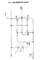
図1に示す本発明の実施形態の入出力バッファ回路におけるNウェル電位制御部A1では、従来技術のNウェル電位制御部A100に加えて、PMOSトランジスタ制御部を備え、第1PMOSトランジスタPM1の導通・非導通を制御している。PMOSトランジスタ制御部は、NMOSトランジスタNM1、第3PMOSトランジスタPM3、そして第1、第2電圧降圧部11、12を備えている。第1PMOSトランジスタPM1のゲート端子と入出力端子PADとの間に、ゲート端子を電源電圧VDD1に、バックゲート端子をNウェルNWに接続した、第3PMOSトランジスタPM3を備えている。更に、NMOSトランジスタNM1を、ドレイン端子を入出力端子PADに、ソース端子を必要に応じて第1電圧降圧部12を介して第1PMOSトランジスタPM1のゲート端子P1に接続して備えている。そして、このゲート端子は、第2電圧降圧部11によりバイアスされている。
【0034】
第2電圧降圧部11は、電源電圧VDD1より低い所定電圧を出力し、NMOSトランジスタNM1のゲート端子を所定電圧にバイアスする。NMOSトランジスタNM1のドレイン端子に入力される入出力端子PADからの電圧信号VINが、所定電圧からNMOSトランジスタNM1の閾値電圧VthNを減じた電圧値以下である場合には、NMOSトランジスタNM1は線形動作して導通することとなり、NMOSトランジスタNM1のソース端子には電圧信号VINがそのまま出力される。一方、電圧信号VINが昇圧し、所定電圧から閾値電圧VthNを減じた電圧値以上になると、NMOSトランジスタNM1は飽和動作することとなる。即ち、NMOSトランジスタNM1のソース端子には、所定電圧から閾値電圧VthNを減じた電圧が出力されることとなる。この出力電圧は、電圧信号VINが昇圧しても変わることはなく、所定電圧から閾値電圧VthNを減じた電圧に固定される。
【0035】
これにより、第1PMOSトランジスタPM1の導通に際し、ゲート端子P1に印加される電圧は、第1電圧降圧部12による降圧前の状態で、所定電圧から閾値電圧VthNを減じた電圧値以下に制限されることとなる。従って、所定電圧を電源電圧VDD1から適宜に降圧した電圧に設定しておけば、第1電圧降圧部12がなく、NMOSトランジスタNM1のソース端子と第1PMOSトランジスタPM1のゲート端子P1とが直結されていても、第1PMOSトランジスタPM1のゲート端子P1とソース端子との間に閾値電圧VthP以上の電圧が確実に印加される。即ち、NMOSトランジスタNM1の閾値電圧VthNと、第1PMOSトランジスタPM1の閾値電圧VthPとの大小関係に応じて、所定電圧を設定してやれば、第1PMOSトランジスタPM1のゲート端子P1に印加される電圧を、ソース端子の電圧である電源電圧VDD1から閾値電圧VthP以上に降圧された電圧とすることができる。第1PMOSトランジスタPM1は線形動作して導通するので、NウェルNWを確実に電源電圧VDD1にバイアスすることができる。
【0036】
第1電圧降圧部12は、NMOSトランジスタNM1のソース端子からの電圧を降圧して、第1PMOSトランジスタPM1のゲート端子P1をバイアスする。これにより、前述した第2電圧降圧部11の有無に関わらず、第1電圧降圧部12により、NMOSトランジスタNM1のソース端子からの電圧を適宜に降圧した電圧を、第1PMOSトランジスタPM1のゲート端子P1に印加することができる。電圧値に関わりなく、第1PMOSトランジスタPM1のゲート端子P1とソース端子との間に閾値電圧VthP以上の電圧が確実に印加され、第1PMOSトランジスタPM1は線形動作して導通するので、NウェルNWを確実に電源電圧VDD1にバイアスすることができる。
【0037】
この状態は、電圧信号VINが、電源電圧VDD1に比して閾値電圧VthP以上の電圧値に達するまで継続する。そして、電源電圧VDD1に比して閾値電圧VthP以上の電圧値に達した後は、第3PMOSトランジスタPM3が導通することにより、第1PMOSトランジスタPM1のゲート端子P1を電圧信号VINにバイアスして、第1PMOSトランジスタPM1を非導通とする。同時に、第2PMOSトランジスタPM2を導通するので、NウェルNWは、電源電圧VDD1代えて、電圧信号VINにバイアスされる。
【0038】
図1に示す本発明の実施形態において、入出力バッファ回路1に備えられるPMOSトランジスタのNウェルNWの電位VNWは、入出力端子PADに印加される電圧信号VINに応じて、VIN<VDD1+VthPの時は電源電圧VDD1に、VIN>VDD1+VthPの時は、電圧信号VINに、切れ目なくバイアスされるので、フローティング状態となることはない。従って、入出力端子PADの電圧信号VINにおけるあらゆる電圧値に対して、NウェルNWの電位VNWを確実に設定することができ、入出力バッファ回路1において、入力状態、出力状態を問わず、常に安定した回路動作を得ることができる。
【0039】
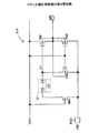
以下、第2電圧降圧部11、及び第1電圧降圧部12の具体例を、図2乃至図6において第1乃至第5具体例として示す。ここで、第1乃至第3具体例(図2乃至図4)は、第2電圧降圧部11の具体例であり、第4、第5具体例(図5、図6)は、第1電圧降圧部12の具体例である。
【0040】
先ず、第2電圧降圧部11の具体例を示す。図2の第1具体例のNウェル電位制御部A11では、第2電圧降圧部11から出力される電源電圧VDD1より低い所定電圧として、複数の電源系統のうちの1つの電源系統である第2の電源電圧VDD2を利用する態様を示している。近年のLSIや、電子応用製品の基板上においては、回路動作を行わせるための電源電圧は、複数系統用意されている場合がある。そこで、これらの電源系統のうち、入出力バッファ回路1の回路動作に使用される電源電圧VDD1に比して低電圧の第2の電源電圧VDD2をNMOSトランジスタNM1のゲート端子バイアス用の電圧として利用することができる。これにより、第1PMOSトランジスタPM1を導通する際には、第1PMOSトランジスタPM1のゲート端子P1に直結されたNMOSトランジスタNM1のソース端子には、第2の電源電圧VDD2から閾値電圧VthNを減じた電圧を上限とした電圧が印加されることとなる。ここで、VDD2<VDD1であるので、第1PMOSトランジスタPM1のゲート・ソース間には、閾値電圧VthP以上の電圧が印加され、第1PMOSトランジスタPM1は、線形動作して導通することとなる。従って、NウェルNWには、電源電圧VDD1が確実にバイアスされることとなる。
【0041】
図3の第2具体例のNウェル電位制御部A12では、第2電圧降圧部11として、電源電圧VDD1と接地電圧GNDとの間に抵抗素子R1、R2を挿入することにより、電源電圧VDD1を分圧した所定電圧をNMOSトランジスタNM1のゲート端子に印加する構成である。抵抗素子R1、R2の分圧比を適宜に設定してやれば、この所定電圧から閾値電圧VthNを減じた電圧が、第1PMOSトランジスタPM1のゲート端子P1に印加され、第1PMOSトランジスタPM1を確実に導通させて、NウェルNWには、電源電圧VDD1が確実にバイアスされる。
【0042】
図4の第3具体例のNウェル電位制御部A13では、第2電圧降圧部11として、所定数のダイオードを直列接続したダイオード群D1により生成した降圧電圧をNMOSトランジスタNM1のゲート端子に印加する。ダイオード群D1の降圧値を適宜に設定してやれば、第1PMOSトランジスタPM1を確実に導通させ、NウェルNWには、電源電圧VDD1が確実にバイアスされる。
【0043】
次に、第1電圧降圧部12の具体例を示す。図5の第4具体例のNウェル電位制御部A14では、第1電圧降圧部12として、所定数のダイオードを直列接続したダイオード群D2により、NMOSトランジスタNM1のソース端子から出力される電圧を降圧して第1PMOSトランジスタPM1のゲート端子P1に印加している。NMOSトランジスタNM1のソース端子から出力される電圧は、電源電圧VDD1から閾値電圧VthNを減じた電圧値を上限としているので、ダイオード群D2の降圧値を適宜に設定することにより、第1PMOSトランジスタPM1を導通する際には、第1PMOSトランジスタPM1のゲート端子P1には、電源電圧VDD1から閾値電圧VthPを減じた電圧以下の電圧を印加することができる。第1PMOSトランジスタPM1は、線形動作して導通することとなり、NウェルNWには、電源電圧VDD1が確実にバイアスされることとなる。
【0044】
図6の第5具体例のNウェル電位制御部A15では、第1電圧降圧部12として、NMOSトランジスタNM1のソース端子と接地電圧GNDとの間に抵抗素子R3、R4を挿入することにより、NMOSトランジスタNM1のソース端子からの電圧を、分圧した所定電圧をPMOSトランジスタPM1のゲート端子P1に印加する構成である。抵抗素子R3、R4の分圧比を適宜に設定してやれば、第1PMOSトランジスタPM1を確実に導通させて、NウェルNWには、電源電圧VDD1が確実にバイアスされることとなる。
【0045】
図7に、実施形態のNウェル電位制御部A1(第1乃至第5具体例A11乃至A15)において、電圧信号VINに対して、ウェルNWの電位VNWの切り替わり波形を、第1PMOSトランジスタPM1のゲート端子P1の電圧値VP1と共に示す。図7においては、電源電圧VDD1を3.3Vとし、NMOS/PMOSトランジスタの閾値電圧の絶対値が略等しい場合(VthN≒VthP)を例として示している。
【0046】
電圧信号VINが、電源電圧VDD1に閾値電圧VthPを加えた電圧以上の場合(図7における、領域(2):VIN>VDD1+VthP)には、第3PMOSトランジスタPM3が導通して、第1PMOSトランジスタPM1のゲート端子P1の電圧値VP1を、電圧信号VINにバイアスするので、第1PMOSトランジスタPM1は非導通となる。一方、第2PMOSトランジスタPM2は導通し、NウェルNWの電位VNWは、電圧信号VINとなる。
【0047】
電圧信号VINが、電源電圧VDD1に閾値電圧VthPを加えた電圧以下に降圧すると(図7における、領域(1)、(3):VIN<VDD1+VthP)、第2及び第3PMOSトランジスタPM2、PM3は非導通となる。一方、NMOSトランジスタNM1は導通する。但し、電圧信号VINがNMOSトランジスタNM1のゲート端子の電圧から閾値電圧VthNを減じた電圧に降圧するまでは、NMOSトランジスタNM1は飽和動作をするため、ソース端子の電圧は、ゲート端子の電圧から閾値電圧VthNを減じた電圧に略固定される。この電圧が、第1PMOSトランジスタPM1のゲート端子P1に印加され、ゲート・ソース間の電位差が閾値電圧VthP以上にバイアスされることにより、第1PMOSトランジスタPM1は線形動作して導通し、NウェルNWが電源電圧VDD1にバイアスされる。
【0048】
図7において、ゲート端子P1の電圧VP1が、電源電圧VDD1(3.3V)から、略閾値電圧VthNだけ降圧した場合の波形は、図1において、第2電圧降圧部11、及び第1電圧降圧部12が共に無く、NMOSトランジスタNM1のゲート端子を電源電圧VDD1に接続した場合の波形である。第1PMOSトランジスタPM1のゲート端子P1には、ソース端子から閾値電圧VthNだけ降圧した電圧が印加されることとなるが、閾値電圧VthNとVthPとが絶対値として略等しいため、第1PMOSトランジスタPM1を充分に線形動作させて導通させることができない虞がある。
【0049】
そこで、第1PMOSトランジスタPM1のゲート端子P1の電圧VP1を更に降圧させるために、第2電圧降圧部11、あるいは第1電圧降圧部12の少なくとも何れか一方を備えることが好ましい。
【0050】
第2電圧降圧部11を備えてやれば、NMOSトランジスタNM1において、ゲート端子に印加する所定電圧を電源電圧VDD1より降圧させることができ、飽和動作するソース端子の電圧値を更に降圧させることができる。この結果、ゲート端子P1の電圧VP1における電源電圧VDD1からの総降圧値V1、V2は、閾値電圧VthNに、第2電圧降圧部11によるゲート端子での所定電圧の降圧値が加算された電圧となる。第2電圧降圧部11を備える場合には、NMOSトランジスタNM1のゲート端子に印加される電圧が降圧されるので、NMOSトランジスタNM1の飽和動作は、総降圧値V1、V2に応じて領域(1)においても維持されることとなる(図7中、Iで指示した波形)。
【0051】
また、第1電圧降圧部12を備えてやれば、ゲート端子P1の電圧VP1を、一律に降圧させることができる。電源電圧VDD1からの総降圧値V1、V2は、閾値電圧VthNに、第1電圧降圧部12による降圧値が加算された電圧である。第1電圧降圧部12を備える場合には、NMOSトランジスタNM1のゲート端子に印加される電圧は、例えば、電源電圧VDD1とすることができるので、NMOSトランジスタNM1の飽和動作は、総降圧値V1、V2に関わらず領域(3)においてのみ維持されることとなる。更に、第1電圧降圧部12による降圧は、一定電圧値となるので、NMOSトランジスタNM1が線形動作をする領域(1)においても、所定電圧の降圧を維持する(図7中、IIで指示した波形)。
【0052】
尚、上記では、第2電圧降圧部11と第1電圧降圧部12とを単独で備える場合について説明したが、第2電圧降圧部11と第1電圧降圧部12とを共に備えてやれば、各々の降圧が加算され、第1PMOSトランジスタPM1の導通時にゲート端子P1に印加される電圧VINを有効に降圧させることができる。即ち、第2電圧降圧部11と第1電圧降圧部12とは、両者を共に備えても各々を単独に備えても同様の効果を奏することができる。
【0053】
また、実施形態では、NMOSトランジスタNM1及び第3PMOSトランジスタPM3とを、第1PMOSトランジスタPM1のゲート端子P1と入出力端子PADとの間に備える場合について説明したが、他の実施形態として、これらの接続関係を逆転させても同様の効果を奏することができる。即ち、NMOSトランジスタNM1及び第3PMOSトランジスタPM3を、第2PMOSトランジスタPM2のゲート端子P2と電源電圧VDD1との間に備え、NMOSトランジスタNM1のゲート端子を入出力端子PADに接続する。また、第1、第3PMOSトランジスタPM1、PM3のゲート端子は、入出力端子PADに接続する。この場合、第2電圧降圧部11、第1電圧降圧部12については実施形態と同様な接続とすることができ、同様の作用・効果を奏する。即ち、第2電圧降圧部11は、NMOSトランジスタNM1のゲート端子に接続して所定電圧を印加させるようにし、入出力端子PADの電圧信号VINを降圧するように設定することもできる。第1電圧降圧部12は、NMOSトランジスタNM1と第2PMOSトランジスタPM2のゲート端子P2との間に備えることができる。
【0054】
他の実施形態において、電圧信号VINに対する、第2PMOSトランジスタPM2のゲート端子P2の電圧VP2及びNウェルNWの電位VNWについての関係を示した波形を図8に示す。領域(1')では、第1、第3PMOSトランジスタPM1、PM3が導通して、第2PMOSトランジスタPM2が非導通となるため、NウェルNWは、電源電圧VDD1にバイアスされる。
【0055】
第2電圧降圧部11と第1電圧降圧部12とを備えない場合には、NMOSトランジスタNM1が飽和動作する領域(3')において、第2PMOSトランジスタPM2のゲート端子P2の電圧VP2は、電圧信号VINから閾値電圧VthNを減じた電圧がバイアスされる。この状態で、NMOS/PMOSの両閾値電圧の絶対値が略等しい(VthN≒VthP)とすると、図7に示した実施形態の場合と同様に、第2PMOSトランジスタPM2が充分に線形動作して導通しない虞がある。
【0056】
また、領域(2')になると、NMOSトランジスタNM1は、線形動作する領域となるので、第2PMOSトランジスタPM2のゲート端子P2の電圧VP2には、電源電圧VDD1が印加され、第2PMOSトランジスタPM2は、線形動作してNウェルNWを電圧信号VINにバイアスする。
【0057】
次に、第2電圧降圧部11を備えると、NMOSトランジスタNM1のゲート端子への印加電圧が降圧するので、この降圧分だけNMOSトランジスタNM1の飽和動作領域が伸びることとなる(図8中、Iで指示した波形)。
【0058】
また、第1電圧降圧部12を備えると、ゲート端子P2の電圧VP2を、一律に降圧させることができる(図8中、IIで指示した波形)。
【0059】
尚、本発明は前記実施形態に限定されるものではなく、本発明の趣旨を逸脱しない範囲内で種々の改良、変形が可能であることは言うまでもない。
例えば、本実施形態においては、MOSトランジスタの閾値電圧VthN、VthPを利用することにより、NウェルNWの電位VNWのバイアス電圧を切り替えるべき電圧信号VINを設定するようにしたが、本発明はこれに限定されるものではなく、電圧信号を検出することができる構成であれば適用することができる。電圧信号が、電源電圧に比して、第1所定電圧値以下であるか、第2所定電圧値以上であるかを検出すればよい。
【0060】
具体的には、これらの第1所定電圧値及び第2所定電圧値をオフセット電圧とするコンパレータ等を構成することにより検出することができる。この場合、コンパレータ等の出力信号により、第1あるいは第2PMOSトランジスタを確実に非導通に制御するため、出力信号の信号レベルを、電源電圧と、入出力端子に入力される電圧信号とのうち高い電圧レベルで制御する必要がある。そこで、第1PMOSトランジスタが非導通となるのは、電圧信号が、コンパレータ等に設定した出力反転電圧以上においてであり、電源電圧より高電圧領域を含む。従って、第1PMOSトランジスタを非導通とする信号を出力するコンパレータ等は、電圧信号で駆動することが好ましい。逆に、第2PMOSトランジスタが非導通となるのは、電圧信号が、コンパレータ等に設定した出力反転電圧以下においてであり、電源電圧より低電圧領域を含む。従って、第2PMOSトランジスタを非導通とする信号を出力するコンパレータ等は、電源電圧で駆動することが好ましい。
【0061】
(付記1) 自己の電源電圧に比して高い電圧レベルの電圧信号が、入出力端子に直接入力される入出力バッファ回路において、
前記電圧信号がドレイン端子に印加されるPMOSトランジスタのNウェル電位を、
前記電圧信号が、前記電源電圧に比して第1所定電圧値以下の電圧となる第1領域では前記電源電圧に、
前記電圧信号が、前記電源電圧に比して第2所定電圧値以上の電圧となる第2領域では前記電圧信号に、
前記電圧信号が、前記第1及び第2領域に挟まれた電圧となる第3領域では前記電源電圧、あるいは前記電圧信号に設定するNウェル電位制御部を備えることを特徴とする入出力バッファ回路。
(付記2) 前記Nウェル電位制御部は、
ソース端子が前記電源電圧に接続され、ドレイン端子及びバックゲート端子が前記Nウェルに接続される第1PMOSトランジスタと、
ソース端子が前記入出力端子に接続され、ドレイン端子及びバックゲート端子が前記Nウェルに接続され、更にゲート端子が前記電源電圧に接続される第2PMOSトランジスタと、
前記第2所定電圧値を、前記第1PMOSトランジスタの閾値電圧値とし、前記第1及び第3領域において、前記第1PMOSトランジスタを導通し、前記第2領域において、前記第1PMOSトランジスタを非導通にするPMOSトランジスタ制御部とを備えることを特徴とする付記1に記載の入出力バッファ回路。
(付記3) 前記PMOSトランジスタ制御部は、
ソース端子が前記第1PMOSトランジスタのゲート端子に、ドレイン端子が前記入出力端子に接続され、ゲート端子に前記電源電圧より低い所定電圧が印加されるNMOSトランジスタと、
ソース端子が前記入出力端子に、ドレイン端子が前記第1PMOSトランジスタのゲート端子に、ゲート端子が前記電源電圧に、バックゲート端子が前記Nウェルに接続される第3PMOSトランジスタとを備えることを特徴とする付記2に記載の入出力バッファ回路。
(付記4) 前記所定電圧は、複数の電源系統のうちの1つの電源系統を利用することを特徴とする付記3に記載の入出力バッファ回路。
(付記5) 前記PMOSトランジスタ制御部は、
ドレイン端子が前記入出力端子に接続されるNMOSトランジスタと、
前記NMOSトランジスタのソース端子からの電圧信号を降圧して、第1PMOSトランジスタのゲート端子に入力する第1電圧降圧部と、
ソース端子が前記入出力端子に、ドレイン端子が前記第1PMOSトランジスタのゲート端子に、ゲート端子が前記電源電圧に、バックゲート端子が前記Nウェルに接続される第3PMOSトランジスタとを備えることを特徴とする付記2乃至4の少なくとも何れか1項に記載の入出力バッファ回路。
(付記6) 前記Nウェル電位制御部は、
ソース端子が前記電源電圧に接続され、ドレイン端子及びバックゲート端子が前記Nウェルに接続され、更にゲート端子が前記入出力端子に接続される第1PMOSトランジスタと、
ソース端子が前記入出力端子に接続され、ドレイン端子及びバックゲート端子が前記Nウェルに接続される第2PMOSトランジスタと、
前記第1所定電圧値を、前記第2PMOSトランジスタの閾値電圧値とし、前記第1領域において、前記第2PMOSトランジスタを非導通とし、前記第2及び第3領域において、前記第2PMOSトランジスタを導通するPMOSトランジスタ制御部とを備えることを特徴とする付記1に記載の入出力バッファ回路。
(付記7) 前記PMOSトランジスタ制御部は、
ソース端子が前記第2PMOSトランジスタのゲート端子に、ドレイン端子が前記電源電圧に接続され、ゲート端子に前記電圧信号、あるいは前記電圧信号より低い所定電圧が印加されるNMOSトランジスタと、
ソース端子が前記電源電圧に、ドレイン端子が前記第2PMOSトランジスタのゲート端子に、ゲート端子が前記入出力端子に、バックゲート端子が前記Nウェルに接続される第3PMOSトランジスタとを備えることを特徴とする付記6に記載の入出力バッファ回路。
(付記8) 前記PMOSトランジスタ制御部は、
ドレイン端子が前記電源電圧に接続されるNMOSトランジスタと、
前記NMOSトランジスタのソース端子からの電圧信号を降圧して、第2PMOSトランジスタのゲート端子に入力する第1電圧降圧部と、
ソース端子が前記電源電圧に、ドレイン端子が前記第2PMOSトランジスタのゲート端子に、ゲート端子が前記入出力端子に、バックゲート端子が前記Nウェルに接続される第3PMOSトランジスタとを備えることを特徴とする付記6又は7に記載の入出力バッファ回路。
(付記9) 前記電源電圧あるいは前記電圧信号の電圧レベルを降圧して、前記所定電圧を出力する第2電圧降圧部を備えることを特徴とする付記3又は7に記載の入出力バッファ回路。
(付記10) 前記第1あるいは第2電圧降圧部は、抵抗素子による電圧降圧を利用することを特徴とする付記5、8又は9の少なくとも何れか1項に記載の入出力バッファ回路。
(付記11) 前記第1あるいは第2電圧降圧部は、接合における電圧降圧を利用することを特徴とする付記5、8又は9の少なくとも何れか1項に記載の入出力バッファ回路。
【0062】
【発明の効果】
本発明によれば、PMOSトランジスタを含む入出力バッファ回路において、自己の電源電圧とは異なる電圧レベルの電圧信号が入出力端子に直接入力されても、Nウェル電位を確実にバイアスすることができ、電圧レベルの全ての領域において、Nウェル電位がフローティング状態にならないNウェル電位制御部を備えた入出力バッファ回路を提供することが可能となる。
【図面の簡単な説明】
【図1】 本発明の実施形態の入出力バッファ回路におけるNウェル電位制御部を示す回路図である。
【図2】 Nウェル電位制御部の第1具体例を示す回路図である。
【図3】 Nウェル電位制御部の第2具体例を示す回路図である。
【図4】 Nウェル電位制御部の第3具体例を示す回路図である。
【図5】 Nウェル電位制御部の第4具体例を示す回路図である。
【図6】 Nウェル電位制御部の第5具体例を示す回路図である。
【図7】 実施形態のNウェル電位制御部によるウェル電位の切り替わりの様子を示す波形図である。
【図8】 他の実施形態のNウェル電位制御部によるウェル電位の切り替わりの様子を示す波形図である。
【図9】 入出力バッファ回路を示す回路ブロック図である。
【図10】 従来技術のNウェル電位制御部を示す回路図である。
【符号の説明】
1 入出力バッファ回路
11 第2電圧降圧部
12 第1電圧降圧部
A1、A11、A12、A13、A14、A15、A100
Nウェル電位制御部
D1、D2 ダイオード群
NM1 NMOSトランジスタ
NW Nウェル
PAD 入出力端子
PM1 第1PMOSトランジスタ
PM2 第2PMOSトランジスタ
PM3 第3PMOSトランジスタ
R1、R2、R3、R4 抵抗素子
VDD1 電源電圧
VDD2 第2の電源電圧[0001]
BACKGROUND OF THE INVENTION
The present invention relates to an input / output buffer circuit, and more particularly to an input / output buffer circuit including a PMOS transistor in which a voltage signal having a voltage level higher than its own power supply voltage is directly input to an input / output terminal. is there.
[0002]
[Prior art]
An input / output buffer circuit is a buffer circuit that can output a signal to the outside of a semiconductor integrated circuit (hereinafter referred to as an LSI) and can receive a signal from the outside and can propagate the signal bidirectionally. As an example, an input /
[0003]
In FIG. 9, the input /
[0004]
The electrostatic breakdown protection unit D is composed of diode elements DU and DL for absorbing the surge voltage input from the input / output terminal PAD into the power supply voltage VDD1 and the ground voltage GND. These diode elements DU and DL can be composed of PN junctions or can be composed of diode-connected MOS transistors. For example, in order to configure the diode element DU with a PMOS transistor, the source terminal, the gate terminal, and the back gate terminal are connected to the power supply voltage VDD1, and the drain terminal is connected to the input / output terminal PAD. When a surge voltage equal to or higher than the threshold voltage of the diode-connected PMOS transistor is applied to the input / output terminal PAD from the power supply voltage VDD1, the diode element DU composed of the PMOS transistor becomes conductive, and the surge voltage is reduced. By forming a path for escape to the power supply voltage VDD1 side, the internal circuit such as the input / output buffer B is protected from surge voltage.
[0005]
The clamp part C is a circuit for clamping the voltage level when the input / output terminal PAD is in a floating state. The PMOS transistor CM1 controlled by the pull-up control circuit C1 conducts as necessary, thereby clamping the input / output terminal PAD to the power supply voltage VDD1.
[0006]
With recent advances in LSI miniaturization and the like, the LSI drive power supply voltage has decreased, and a system may be configured by combining a plurality of LSIs that operate with different power supply voltages. At this time, it is convenient if the input / output terminals of LSIs operating with different power supply voltages can be directly connected, and proposals for realizing this have been made. This proposal includes an N-well potential controller A that biases the N-well potential of the PMOS transistor on the high voltage side of the power supply voltage and the input voltage signal. Specifically, the following method is used. is there.
[0007]
The N well potential control unit A100 shown in FIG. 10 has a source terminal connected to the power supply voltage VDD1, a drain terminal and a back gate terminal connected to the N well NW, and a gate terminal connected to the input / output terminal PAD (input / output voltage). A first PMOS transistor PM1 connected to the signal VIN), a second PMOS transistor having a source terminal connected to the input / output terminal PAD, a drain terminal and a back gate terminal connected to the N well NW, and a gate terminal connected to the power supply voltage VDD1. It is comprised by PM2.
[0008]
When the threshold voltage of the PMOS transistors PM1 and PM2 is VthP, when VIN <VDD1-VthP, the voltage signal VIN applied to the gate terminal of the first PMOS transistor PM1 is compared with the power supply voltage VDD1 applied to the source terminal. The potential difference is lower than the threshold voltage VthP. Therefore, the first PMOS transistor PM1 conducts linearly and becomes conductive, and the N well NW and the power supply voltage VDD1 are connected. On the other hand, in the second PMOS transistor PM2, the voltage relationship between the gate terminal and the source terminal is opposite to that of the first PMOS transistor PM1, and therefore the non-conducting state is maintained. Therefore, the potential VNW of the N well NW is biased to the power supply voltage VDD1.
[0009]
When VIN> VDD1 + VthP, the voltage relationship between the gate terminal and the source terminal of the first and second PMOS transistors PM1 and PM2 is opposite to the above. That is, the first PMOS transistor PM1 becomes non-conductive while the second PMOS transistor PM2 conducts linearly and becomes conductive. Therefore, the potential VNW of the N well NW is biased to the voltage signal VIN.
[0010]
In the N well potential control unit A100 of FIG. 10, the N well NW is biased to the power supply voltage VDD1 when VIN <VDD1-VthP, and is biased to the voltage signal VIN when VIN> VDD1 + VthP. In these regions, the N well NW is biased to the higher voltage side of the power supply voltage VDD1 and the voltage signal VIN.
[0011]
[Problems to be solved by the invention]
However, in the N well potential control unit A100, the N well NW is in a floating state in the region of VDD1-VthP <VIN <VDD1 + VthP, which is a problem.
[0012]
As described above, when the potential VNW of the N well NW is in a floating state, the drive stage PMOS transistor BM1 of the output buffer unit BO, the PMOS transistor CM1 of the clamp unit C, and the PMOS of the electrostatic breakdown protection unit D in FIG. The back gate bias in a PMOS transistor such as a diode element DU composed of a transistor becomes unstable, the driving ability becomes unstable due to the unstable threshold voltage due to the back gate bias effect, the switching control becomes unstable, or Various problems in circuit operation such as an increase in forward current at the PN junction from the drain terminal to the N well NW may occur, which is a problem.
[0013]
The present invention has been made to solve the problems of the prior art, and in an input / output buffer circuit including a PMOS transistor, a voltage signal having a voltage different from its own power supply voltage is directly input to the input / output terminal. Another object of the present invention is to provide an input / output buffer circuit including an N-well potential control unit that can reliably bias an N-well potential and does not enter a floating state in the entire voltage range of the voltage signal. To do.
[0014]
[Means for Solving the Problems]
In order to achieve the above object, an input / output buffer circuit according to
[0015]
According to another aspect of the input / output buffer circuit of the present invention, the N well potential control unit converts the N well potential of the PMOS transistor, to which the voltage signal is applied to the drain terminal, to the power supply voltage according to the voltage level of the voltage signal at the input / output terminal. Switch appropriately between voltage signals. The voltage level of the voltage signal to be switched is determined according to the magnitude relationship with the power supply voltage. That is, the voltage signal is set to the power supply voltage in the first region where the voltage signal is equal to or lower than the first predetermined voltage value compared to the power supply voltage, and is set to the voltage equal to or higher than the second predetermined voltage value compared to the power supply voltage. In the area, the voltage signal is set. In the intermediate third region, one of the voltage levels is set.In this case, since the source terminal of the second PMOS transistor is connected to the input / output terminal and the gate terminal is connected to the power supply voltage, the voltage level of the voltage signal is equal to or higher than the voltage obtained by adding the threshold voltage of the second PMOS transistor to the power supply voltage. The second PMOS transistor is turned on to supply a voltage signal to the N well. Meanwhile, the first PMOS transistor is controlled by a PMOS transistor controller. The voltage level of the voltage signal is obtained by adding the threshold voltage of the second PMOS transistor to the power supply voltage as a threshold voltage. In the first and third regions below this voltage, the power supply voltage is supplied to the N well. It becomes non-conductive in the second region above the voltage. Usually, the threshold voltages of the first and second PMOS transistors are the same. Therefore, in the first and third regions, the second PMOS transistor is turned off and the first PMOS transistor is turned on to set the N-well potential to the power supply voltage. In the second region, the first PMOS transistor is turned off and the second PMOS transistor is turned off. The transistor becomes conductive and makes the N well potential a voltage signal.
The input / output buffer circuit according to claim 4 is an input / output buffer circuit in which a voltage signal having a voltage level higher than its own power supply voltage is directly input to the input / output terminal, and the voltage signal is applied to the drain terminal. The PMOS transistor N-well potential is set to the power supply voltage in the first region where the voltage signal is equal to or lower than the first predetermined voltage value compared to the power supply voltage, and the voltage signal is compared to the power supply voltage. 2 N well set to the voltage signal in the second region where the voltage is equal to or higher than a predetermined voltage value, the voltage signal is set to the power supply voltage or the voltage signal in the third region where the voltage is sandwiched between the first and second regions The N-well potential control unit includes first and second PMOS transistors, and the source terminal, the drain terminal, and the back gate terminal are connected in the same manner as in
5. The input / output buffer circuit according to claim 4, wherein the voltage signal is drained by the N well potential control unit. The N-well potential of the PMOS transistor applied to the terminal is appropriately switched between the power supply voltage and the voltage signal according to the voltage level of the voltage signal at the input / output terminal. The voltage level of the voltage signal to be switched is determined according to the magnitude relationship with the power supply voltage. That is, the voltage signal is set to the power supply voltage in the first region where the voltage signal is equal to or lower than the first predetermined voltage value compared to the power supply voltage, and is set to the voltage equal to or higher than the second predetermined voltage value compared to the power supply voltage. In the area, the voltage signal is set. In the intermediate third region, one of the voltage levels is set. In this case, the connection of the first and second PMOS transistors to the gate terminals is opposite to the connection in
[0016]
As a result, the N-well potential of the PMOS transistor is set to an appropriate voltage according to the voltage level of the voltage signal applied to the input / output terminal, and therefore does not enter a floating state at a predetermined voltage level. Therefore, the N well potential can be reliably set for every voltage level in the voltage signal of the input / output terminal, and the input / output buffer circuit always obtains a stable circuit operation regardless of the input state or the output state. be able to.
Using the threshold voltage of the PMOS transistor, the N-well potential can be switched between the power supply voltage and the voltage signal, with the voltage level of the voltage signal separated from the power supply voltage by the threshold voltage as a boundary.
[0017]
The input / output buffer circuit according to
[0018]
[0019]
[0020]
[0021]
[0022]
[0023]
Claims3An input / output buffer circuit according to claim1 or 2In the input / output buffer circuit described in (1), the PMOS transistor control unit includes an NMOS in which a source terminal is connected to the gate terminal of the first PMOS transistor, a drain terminal is connected to the input / output terminal, and a predetermined voltage lower than the power supply voltage is applied to the gate terminal. And a third PMOS transistor having a source terminal connected to the input / output terminal, a drain terminal connected to the gate terminal of the first PMOS transistor, a gate terminal connected to the power supply voltage, and a back gate terminal connected to the N-well. .
[0024]
Claim3In the input / output buffer circuit, as a PMOS transistor control unit for controlling the first PMOS transistor, a predetermined voltage lower than the power supply voltage is applied to the gate terminal of the NMOS transistor, so that the input terminal is connected between the input / output terminal and the gate terminal of the first PMOS transistor. It is connected to the. Then, a voltage having an upper limit obtained by subtracting the threshold voltage of the NMOS transistor from a predetermined voltage lower than the power supply voltage is applied to the gate terminal of the first PMOS transistor to make the first PMOS transistor conductive. On the other hand, when the voltage level of the voltage signal is boosted above the threshold voltage of the third PMOS transistor in addition to the power supply voltage, the third PMOS transistor is turned on, and the voltage signal is applied to the gate terminal of the first PMOS transistor, so that the NMOS transistor Is turned off. Usually, since the threshold values of the first to third PMOS transistors coincide with each other, the third PMOS transistor makes the NMOS transistor non-conductive and also makes the first PMOS transistor non-conductive. Since the second PMOS transistor becomes conductive, the N-well potential is switched.
[0025]
Claims5An input / output buffer circuit according to claim4In the input / output buffer circuit described in (2), the PMOS transistor controller has a source terminal connected to the gate terminal of the second PMOS transistor, a drain terminal connected to the power supply voltage, and a voltage signal or a predetermined voltage lower than the voltage signal applied to the gate terminal. And a third PMOS transistor having a source terminal connected to the power supply voltage, a drain terminal connected to the gate terminal of the second PMOS transistor, a gate terminal connected to the input / output terminal, and a back gate terminal connected to the N well. Features.
[0026]
Claim5In the input / output buffer circuit, as the PMOS transistor control unit for controlling the second PMOS transistor, the NMOS transistor has a voltage signal applied to the gate terminal or a predetermined voltage lower than the voltage signal, and the power supply voltage and the gate terminal of the second PMOS transistor. Connected between and. Then, a voltage obtained by subtracting the threshold voltage of the NMOS transistor from the voltage signal or a predetermined voltage lower than the voltage signal is applied to the gate terminal of the second PMOS transistor to make the second PMOS transistor conductive. On the other hand, when the voltage level of the voltage signal drops below the threshold voltage of the third PMOS transistor from the power supply voltage, the third PMOS transistor becomes conductive, the power supply voltage is applied to the gate terminal of the second PMOS transistor, and the NMOS transistor is turned off. Conducted. Usually, since the threshold values of the first to third PMOS transistors coincide with each other, the third PMOS transistor makes the NMOS transistor non-conductive and the second PMOS transistor non-conductive. Since the first PMOS transistor becomes conductive, the N-well potential is switched.
[0027]
Thus, when the NMOS transistor conducts the first or second PMOS transistor, the voltage applied to the gate terminal of the first or second PMOS transistor is changed from the voltage applied to the gate terminal of the NMOS transistor to the threshold voltage of the NMOS transistor. Therefore, a voltage equal to or higher than the threshold voltage can be reliably applied between the gate terminal and the source terminal of the first or second PMOS transistor. In particular, if the voltage applied to the gate terminal of the NMOS transistor is a predetermined voltage lower than the power supply voltage or the voltage signal, the upper limit of the voltage applied to the gate terminal of the first or second PMOS transistor is lowered by the predetermined voltage. can do. The first or second PMOS transistor can be linearly operated to be conductive, and the N well can be reliably biased to the power supply voltage or the voltage signal.
[0028]
Where the claim3In the input / output buffer circuit described in (1), the predetermined voltage applied to the gate terminal of the NMOS transistor can use one of the plurality of power supply systems.
[0029]
In addition, if a second voltage step-down unit that receives a power supply voltage or voltage signal and outputs a predetermined voltage is provided, the predetermined voltage applied to the gate terminal of the NMOS transistor is appropriately stepped down from the power supply voltage or voltage signal. Can be provided.
[0030]
In addition, if the first voltage step-down unit that receives a signal from the source terminal of the NMOS transistor and outputs a signal stepped down from the signal to the gate terminal of the first or second PMOS transistor is provided, the first or second PMOS transistor When the transistor is turned on, the voltage applied to the gate terminal of the first or second PMOS transistor can be appropriately reduced to make the first or second PMOS transistor conductive.
[0031]
Here, as the first and second voltage step-down units, if the step-down by the resistance element or the step-down at the junction is used, an appropriately step-down output can be easily obtained.
[0032]
DETAILED DESCRIPTION OF THE INVENTION
DESCRIPTION OF THE PREFERRED EMBODIMENTS Embodiments of an input / output buffer circuit according to the present invention will be described below in detail with reference to the drawings based on FIGS. FIG. 1 is a circuit diagram showing an N-well potential control unit in the input / output buffer circuit according to the embodiment of the present invention. FIG. 2 is a circuit diagram showing a first specific example of the N-well potential control unit. FIG. 3 is a circuit diagram showing a second specific example of the N-well potential control unit. FIG. 4 is a circuit diagram showing a third specific example of the N-well potential control unit. FIG. 5 is a circuit diagram showing a fourth specific example of the N-well potential control unit. FIG. 6 is a circuit diagram showing a fifth specific example of the N-well potential control unit. FIG. 7 is a waveform diagram showing how the well potential is switched by the N-well potential control unit of the embodiment. FIG. 8 is a waveform diagram showing how the well potential is switched by the N-well potential control unit of another embodiment. FIG. 9 is a circuit block diagram showing the input / output buffer circuit. FIG. 10 is a circuit diagram showing a conventional N-well potential control unit.
[0033]
The N well potential controller A1 in the input / output buffer circuit according to the embodiment of the present invention shown in FIG. 1 includes a PMOS transistor controller in addition to the conventional N well potential controller A100. Non-conduction is controlled. The PMOS transistor control unit includes an NMOS transistor NM1, a third PMOS transistor PM3, and first and second voltage step-down
[0034]
The second voltage step-down
[0035]
Accordingly, when the first PMOS transistor PM1 is turned on, the voltage applied to the gate terminal P1 is limited to a voltage value obtained by subtracting the threshold voltage VthN from the predetermined voltage in a state before the voltage is lowered by the first voltage
[0036]
The first voltage step-down
[0037]
This state continues until the voltage signal VIN reaches a voltage value equal to or higher than the threshold voltage VthP as compared with the power supply voltage VDD1. Then, after reaching a voltage value equal to or higher than the threshold voltage VthP as compared with the power supply voltage VDD1, the third PMOS transistor PM3 is turned on to bias the gate terminal P1 of the first PMOS transistor PM1 to the voltage signal VIN, and 1 PMOS transistor PM1 is turned off. At the same time, since the second PMOS transistor PM2 is rendered conductive, the N well NW is biased to the voltage signal VIN instead of the power supply voltage VDD1.
[0038]
In the embodiment of the present invention shown in FIG. 1, the potential VNW of the N well NW of the PMOS transistor provided in the input /
[0039]
Specific examples of the second voltage step-down
[0040]
First, a specific example of the second voltage step-down
[0041]
In the N-well potential control unit A12 of the second specific example of FIG. 3, as the second voltage step-down
[0042]
In the N well potential control unit A13 of the third specific example of FIG. 4, as the second voltage step-down
[0043]
Next, a specific example of the first voltage step-down
[0044]
In the N-well potential control unit A15 of the fifth specific example of FIG. 6, as the first voltage step-down
[0045]
FIG. 7 shows the switching waveform of the potential VNW of the well NW with respect to the voltage signal VIN in the N well potential control unit A1 (first to fifth specific examples A11 to A15) of the embodiment, and the gate of the first PMOS transistor PM1. It is shown together with the voltage value VP1 of the terminal P1. FIG. 7 shows an example in which the power supply voltage VDD1 is 3.3 V and the absolute values of the threshold voltages of the NMOS / PMOS transistors are substantially equal (VthN≈VthP).
[0046]
When the voltage signal VIN is equal to or higher than the voltage obtained by adding the threshold voltage VthP to the power supply voltage VDD1 (region (2) in FIG. 7: VIN> VDD1 + VthP), the third PMOS transistor PM3 becomes conductive and the first PMOS transistor PM1 Since the voltage value VP1 of the gate terminal P1 is biased to the voltage signal VIN, the first PMOS transistor PM1 becomes non-conductive. On the other hand, the second PMOS transistor PM2 becomes conductive, and the potential VNW of the N well NW becomes the voltage signal VIN.
[0047]
When the voltage signal VIN drops below the voltage obtained by adding the threshold voltage VthP to the power supply voltage VDD1 (regions (1) and (3) in FIG. 7: VIN <VDD1 + VthP), the second and third PMOS transistors PM2 and PM3 are non- It becomes conduction. On the other hand, the NMOS transistor NM1 becomes conductive. However, since the NMOS transistor NM1 operates in saturation until the voltage signal VIN is stepped down to the voltage obtained by subtracting the threshold voltage VthN from the voltage at the gate terminal of the NMOS transistor NM1, the voltage at the source terminal is changed from the voltage at the gate terminal to the threshold value. The voltage is substantially fixed to a voltage obtained by subtracting the voltage VthN. This voltage is applied to the gate terminal P1 of the first PMOS transistor PM1, and the potential difference between the gate and the source is biased to the threshold voltage VthP or more, so that the first PMOS transistor PM1 conducts linearly and becomes conductive. Biased to the power supply voltage VDD1.
[0048]
In FIG. 7, when the voltage VP1 of the gate terminal P1 is stepped down from the power supply voltage VDD1 (3.3V) by approximately the threshold voltage VthN, the waveforms in FIG. 1 are the second voltage step-down
[0049]
Therefore, it is preferable to include at least one of the second voltage step-down
[0050]
If the second voltage step-down
[0051]
If the first voltage step-down
[0052]
In the above description, the case where the second voltage step-down
[0053]
Further, in the embodiment, the case where the NMOS transistor NM1 and the third PMOS transistor PM3 are provided between the gate terminal P1 of the first PMOS transistor PM1 and the input / output terminal PAD has been described. The same effect can be achieved even if the relationship is reversed. That is, the NMOS transistor NM1 and the third PMOS transistor PM3 are provided between the gate terminal P2 of the second PMOS transistor PM2 and the power supply voltage VDD1, and the gate terminal of the NMOS transistor NM1 is connected to the input / output terminal PAD. The gate terminals of the first and third PMOS transistors PM1 and PM3 are connected to the input / output terminal PAD. In this case, the second voltage step-down
[0054]
FIG. 8 shows a waveform showing the relationship between the voltage VP2 of the gate terminal P2 of the second PMOS transistor PM2 and the potential VNW of the N well NW with respect to the voltage signal VIN in another embodiment. In the region (1 ′), the first and third PMOS transistors PM1 and PM3 are turned on and the second PMOS transistor PM2 is turned off, so that the N well NW is biased to the power supply voltage VDD1.
[0055]
When the second voltage step-down
[0056]
In the region (2 ′), the NMOS transistor NM1 is a region that performs a linear operation. Therefore, the power supply voltage VDD1 is applied to the voltage VP2 of the gate terminal P2 of the second PMOS transistor PM2, and the second PMOS transistor PM2 Linearly operates to bias the N well NW to the voltage signal VIN.
[0057]
Next, when the second voltage step-down
[0058]
Further, when the first voltage step-down
[0059]
The present invention is not limited to the above-described embodiment, and it goes without saying that various improvements and modifications can be made without departing from the spirit of the present invention.
For example, in this embodiment, the voltage signal VIN for switching the bias voltage of the potential VNW of the N well NW is set by using the threshold voltages VthN and VthP of the MOS transistor. The present invention is not limited, and any configuration that can detect a voltage signal can be applied. What is necessary is just to detect whether a voltage signal is below a 1st predetermined voltage value or more than a 2nd predetermined voltage value compared with a power supply voltage.
[0060]
Specifically, it can be detected by configuring a comparator or the like using these first predetermined voltage value and second predetermined voltage value as an offset voltage. In this case, in order to reliably control the first or second PMOS transistor to be non-conductive by the output signal from the comparator or the like, the signal level of the output signal is higher between the power supply voltage and the voltage signal input to the input / output terminal. It is necessary to control the voltage level. Therefore, the first PMOS transistor becomes non-conductive when the voltage signal is equal to or higher than the output inversion voltage set in the comparator or the like, and includes a higher voltage region than the power supply voltage. Accordingly, it is preferable to drive the comparator or the like that outputs a signal that makes the first PMOS transistor non-conductive by a voltage signal. Conversely, the second PMOS transistor becomes non-conductive when the voltage signal is equal to or lower than the output inversion voltage set in the comparator or the like, and includes a lower voltage region than the power supply voltage. Therefore, it is preferable to drive the comparator or the like that outputs a signal for turning off the second PMOS transistor with the power supply voltage.
[0061]
(Supplementary note 1) In an input / output buffer circuit in which a voltage signal having a voltage level higher than its own power supply voltage is directly input to the input / output terminal,
The N-well potential of the PMOS transistor, to which the voltage signal is applied to the drain terminal,
In the first region where the voltage signal is a voltage equal to or lower than a first predetermined voltage value compared to the power supply voltage, the power supply voltage is
In the second region where the voltage signal is a voltage equal to or higher than a second predetermined voltage value compared to the power supply voltage, the voltage signal is
An input / output buffer circuit comprising an N-well potential control unit set to the power supply voltage or the voltage signal in a third region where the voltage signal is a voltage sandwiched between the first and second regions .
(Supplementary Note 2) The N well potential control unit includes:
A first PMOS transistor having a source terminal connected to the power supply voltage and a drain terminal and a back gate terminal connected to the N well;
A second PMOS transistor having a source terminal connected to the input / output terminal, a drain terminal and a back gate terminal connected to the N well, and a gate terminal connected to the power supply voltage;
The second predetermined voltage value is a threshold voltage value of the first PMOS transistor, the first PMOS transistor is turned on in the first and third regions, and the first PMOS transistor is turned off in the second region. The input / output buffer circuit according to
(Supplementary Note 3) The PMOS transistor controller is
An NMOS transistor having a source terminal connected to the gate terminal of the first PMOS transistor, a drain terminal connected to the input / output terminal, and a predetermined voltage lower than the power supply voltage applied to the gate terminal;
And a third PMOS transistor having a source terminal connected to the input / output terminal, a drain terminal connected to the gate terminal of the first PMOS transistor, a gate terminal connected to the power supply voltage, and a back gate terminal connected to the N-well. The input / output buffer circuit according to
(Supplementary note 4) The input / output buffer circuit according to
(Supplementary Note 5) The PMOS transistor controller is
An NMOS transistor having a drain terminal connected to the input / output terminal;
A first voltage step-down unit for stepping down a voltage signal from the source terminal of the NMOS transistor and inputting the voltage signal to the gate terminal of the first PMOS transistor;
And a third PMOS transistor having a source terminal connected to the input / output terminal, a drain terminal connected to the gate terminal of the first PMOS transistor, a gate terminal connected to the power supply voltage, and a back gate terminal connected to the N-well. The input / output buffer circuit according to at least one of
(Supplementary Note 6) The N well potential control unit includes:
A first PMOS transistor having a source terminal connected to the power supply voltage, a drain terminal and a back gate terminal connected to the N well, and a gate terminal connected to the input / output terminal;
A second PMOS transistor having a source terminal connected to the input / output terminal and a drain terminal and a back gate terminal connected to the N well;
The first predetermined voltage value is a threshold voltage value of the second PMOS transistor, the second PMOS transistor is turned off in the first region, and the second PMOS transistor is turned on in the second and third regions. The input / output buffer circuit according to
(Appendix 7) The PMOS transistor control unit
An NMOS transistor having a source terminal connected to the gate terminal of the second PMOS transistor, a drain terminal connected to the power supply voltage, and a voltage signal applied to the gate terminal or a predetermined voltage lower than the voltage signal;
And a third PMOS transistor having a source terminal connected to the power supply voltage, a drain terminal connected to the gate terminal of the second PMOS transistor, a gate terminal connected to the input / output terminal, and a back gate terminal connected to the N well. The input / output buffer circuit according to appendix 6.
(Supplementary Note 8) The PMOS transistor controller is
An NMOS transistor having a drain terminal connected to the power supply voltage;
A first voltage step-down unit that steps down a voltage signal from a source terminal of the NMOS transistor and inputs the voltage signal to a gate terminal of a second PMOS transistor;
And a third PMOS transistor having a source terminal connected to the power supply voltage, a drain terminal connected to the gate terminal of the second PMOS transistor, a gate terminal connected to the input / output terminal, and a back gate terminal connected to the N well. The input / output buffer circuit according to appendix 6 or 7.
(Supplementary note 9) The input / output buffer circuit according to
(Supplementary Note 10) The input / output buffer circuit according to at least one of Supplementary Notes 5, 8, and 9, wherein the first or second voltage step-down unit uses voltage step-down by a resistance element.
(Additional remark 11) The said 1st or 2nd voltage step-down part utilizes the voltage step-down in a junction, The input / output buffer circuit of any one of Additional remark 5, 8 or 9 characterized by the above-mentioned.
[0062]
【The invention's effect】
According to the present invention, in an input / output buffer circuit including a PMOS transistor, even when a voltage signal having a voltage level different from its own power supply voltage is directly input to the input / output terminal, the N-well potential can be reliably biased. Thus, it is possible to provide an input / output buffer circuit including an N well potential control unit in which the N well potential is not in a floating state in all regions of the voltage level.
[Brief description of the drawings]
FIG. 1 is a circuit diagram showing an N-well potential control unit in an input / output buffer circuit according to an embodiment of the present invention.
FIG. 2 is a circuit diagram showing a first specific example of an N-well potential control unit.
FIG. 3 is a circuit diagram showing a second specific example of an N-well potential control unit.
FIG. 4 is a circuit diagram showing a third specific example of an N-well potential control unit.
FIG. 5 is a circuit diagram showing a fourth specific example of an N-well potential control unit.
FIG. 6 is a circuit diagram showing a fifth specific example of an N-well potential control unit.
FIG. 7 is a waveform diagram showing how well potentials are switched by the N-well potential control unit according to the embodiment.
FIG. 8 is a waveform diagram showing how well potentials are switched by an N-well potential control unit according to another embodiment.
FIG. 9 is a circuit block diagram showing an input / output buffer circuit.
FIG. 10 is a circuit diagram showing a conventional N-well potential control unit.
[Explanation of symbols]
1 I / O buffer circuit
11 Second voltage step-down unit
12 First voltage step-down unit
A1, A11, A12, A13, A14, A15, A100
N-well potential controller
D1, D2 Diode group
NM1 NMOS transistor
NW N well
PAD input / output terminal
PM1 First PMOS transistor
PM2 Second PMOS transistor
PM3 Third PMOS transistor
R1, R2, R3, R4 resistance elements
VDD1 Power supply voltage
VDD2 Second power supply voltage
Claims (5)
前記電圧信号がドレイン端子に印加されるPMOSトランジスタのNウェル電位を、
前記電圧信号が、前記電源電圧に比して第1所定電圧値以下の電圧となる第1領域では前記電源電圧に、
前記電圧信号が、前記電源電圧に比して第2所定電圧値以上の電圧となる第2領域では前記電圧信号に、
前記電圧信号が、前記第1及び第2領域に挟まれた電圧となる第3領域では前記電源電圧、あるいは前記電圧信号に設定するNウェル電位制御部を備え、
前記Nウェル電位制御部は、
ソース端子が前記電源電圧に接続され、ドレイン端子及びバックゲート端子が前記Nウェルに接続される第1PMOSトランジスタと、
ソース端子が前記入出力端子に接続され、ドレイン端子及びバックゲート端子が前記Nウェルに接続され、更にゲート端子が前記電源電圧に接続される第2PMOSトランジスタと、
前記第2所定電圧値を、前記第2PMOSトランジスタの閾値電圧値とし、前記第1及び第3領域において、前記第1PMOSトランジスタを導通し、前記第2領域において、前記第1PMOSトランジスタを非導通にするPMOSトランジスタ制御部とを備えることを特徴とする入出力バッファ回路。In an input / output buffer circuit in which a voltage signal having a voltage level higher than its own power supply voltage is directly input to the input / output terminal,
The N-well potential of the PMOS transistor, to which the voltage signal is applied to the drain terminal,
In the first region where the voltage signal is a voltage equal to or lower than a first predetermined voltage value compared to the power supply voltage, the power supply voltage is
In the second region where the voltage signal is a voltage equal to or higher than a second predetermined voltage value compared to the power supply voltage, the voltage signal is
In the third region where the voltage signal is a voltage sandwiched between the first and second regions, the power supply voltage, or an N-well potential control unit that is set to the voltage signal ,
The N well potential control unit includes:
A first PMOS transistor having a source terminal connected to the power supply voltage and a drain terminal and a back gate terminal connected to the N well;
A second PMOS transistor having a source terminal connected to the input / output terminal, a drain terminal and a back gate terminal connected to the N well, and a gate terminal connected to the power supply voltage;
The second predetermined voltage value is a threshold voltage value of the second PMOS transistor, and the first PMOS transistor is turned on in the first and third regions, and the first PMOS transistor is turned off in the second region. output buffer circuit according to claim Rukoto a PMOS transistor controller.
ソース端子が前記第1PMOSトランジスタのゲート端子に、ドレイン端子が前記入出力端子に接続され、ゲート端子に前記電源電圧より低い所定電圧が印加されるNMOSトランジスタと、 ソース端子が前記入出力端子に、ドレイン端子が前記第1PMOSトランジスタのゲート端子に、ゲート端子が前記電源電圧に、バックゲート端子が前記Nウェルに接続される第3PMOSトランジスタとを備えることを特徴とする請求項1または2に記載の入出力バッファ回路。The PMOS transistor controller is
An NMOS transistor having a source terminal connected to the gate terminal of the first PMOS transistor, a drain terminal connected to the input / output terminal, and a predetermined voltage lower than the power supply voltage applied to the gate terminal; a source terminal connected to the input / output terminal; the gate terminal of the drain terminal said first 1PMOS transistor, the gate terminal the power supply voltage, the back gate terminal of claim 1 or 2, characterized in that it comprises a first 3PMOS transistor connected to said N-well Input / output buffer circuit.
前記電圧信号がドレイン端子に印加されるPMOSトランジスタのNウェル電位を、
前記電圧信号が、前記電源電圧に比して第1所定電圧値以下の電圧となる第1領域では前記電源電圧に、
前記電圧信号が、前記電源電圧に比して第2所定電圧値以上の電圧となる第2領域では前記電圧信号に、
前記電圧信号が、前記第1及び第2領域に挟まれた電圧となる第3領域では前記電源電圧、あるいは前記電圧信号に設定するNウェル電位制御部を備え、
前記Nウェル電位制御部は、
ソース端子が前記電源電圧に接続され、ドレイン端子及びバックゲート端子が前記Nウェルに接続され、更にゲート端子が前記入出力端子に接続される第1PMOSトランジスタと、
ソース端子が前記入出力端子に接続され、ドレイン端子及びバックゲート端子が前記Nウェルに接続される第2PMOSトランジスタと、
前記第1所定電圧値を、前記第1PMOSトランジスタの閾値電圧値とし、前記第1領域において、前記第2PMOSトランジスタを非導通とし、前記第2及び第3領域において、前記第2PMOSトランジスタを導通するPMOSトランジスタ制御部とを備えることを特徴とする入出力バッファ回路。 In an input / output buffer circuit in which a voltage signal having a voltage level higher than its own power supply voltage is directly input to the input / output terminal,
The N-well potential of the PMOS transistor, to which the voltage signal is applied to the drain terminal,
In the first region where the voltage signal is a voltage equal to or lower than a first predetermined voltage value compared to the power supply voltage, the power supply voltage is
In the second region where the voltage signal is a voltage equal to or higher than a second predetermined voltage value compared to the power supply voltage, the voltage signal is
In the third region where the voltage signal is a voltage sandwiched between the first and second regions, the power supply voltage, or an N-well potential control unit set to the voltage signal,
The N well potential control unit includes:
A first PMOS transistor having a source terminal connected to the power supply voltage, a drain terminal and a back gate terminal connected to the N well, and a gate terminal connected to the input / output terminal;
A second PMOS transistor having a source terminal connected to the input / output terminal and a drain terminal and a back gate terminal connected to the N well;
The first predetermined voltage value is a threshold voltage value of the first PMOS transistor, the second PMOS transistor is turned off in the first region, and the second PMOS transistor is turned on in the second and third regions. input and output buffer circuit you anda PMOS transistor controller.
ソース端子が前記第2PMOSトランジスタのゲート端子に、ドレイン端子が前記電源電圧に接続され、ゲート端子に前記電圧信号、あるいは前記電圧信号より低い所定電圧が印加されるNMOSトランジスタと、
ソース端子が前記電源電圧に、ドレイン端子が前記第2PMOSトランジスタのゲート端子に、ゲート端子が前記入出力端子に、バックゲート端子が前記Nウェルに接続される第3PMOSトランジスタとを備えることを特徴とする請求項4に記載の入出力バッファ回路。The PMOS transistor controller is
An NMOS transistor having a source terminal connected to the gate terminal of the second PMOS transistor, a drain terminal connected to the power supply voltage, and a voltage signal applied to the gate terminal or a predetermined voltage lower than the voltage signal;
And a third PMOS transistor having a source terminal connected to the power supply voltage, a drain terminal connected to the gate terminal of the second PMOS transistor, a gate terminal connected to the input / output terminal, and a back gate terminal connected to the N well. The input / output buffer circuit according to claim 4 .
Priority Applications (1)
| Application Number | Priority Date | Filing Date | Title |
|---|---|---|---|
| JP2001258877A JP4149151B2 (en) | 2001-08-29 | 2001-08-29 | I / O buffer circuit |
Applications Claiming Priority (1)
| Application Number | Priority Date | Filing Date | Title |
|---|---|---|---|
| JP2001258877A JP4149151B2 (en) | 2001-08-29 | 2001-08-29 | I / O buffer circuit |
Publications (2)
| Publication Number | Publication Date |
|---|---|
| JP2003069410A JP2003069410A (en) | 2003-03-07 |
| JP4149151B2 true JP4149151B2 (en) | 2008-09-10 |
Family
ID=19086325
Family Applications (1)
| Application Number | Title | Priority Date | Filing Date |
|---|---|---|---|
| JP2001258877A Expired - Fee Related JP4149151B2 (en) | 2001-08-29 | 2001-08-29 | I / O buffer circuit |
Country Status (1)
| Country | Link |
|---|---|
| JP (1) | JP4149151B2 (en) |
Families Citing this family (3)
| Publication number | Priority date | Publication date | Assignee | Title |
|---|---|---|---|---|
| KR100772427B1 (en) | 2006-08-28 | 2007-11-01 | (주)알파칩스 | Output driver |
| CN106067821B (en) * | 2016-07-20 | 2023-04-14 | 成都博思微科技有限公司 | Protection circuit of high-speed buffer and implementation method thereof |
| DE112022004372T5 (en) * | 2021-10-15 | 2024-07-25 | Rohm Co., Ltd. | OUTPUT DRIVER |
-
2001
- 2001-08-29 JP JP2001258877A patent/JP4149151B2/en not_active Expired - Fee Related
Also Published As
| Publication number | Publication date |
|---|---|
| JP2003069410A (en) | 2003-03-07 |
Similar Documents
| Publication | Publication Date | Title |
|---|---|---|
| KR960003374B1 (en) | Semiconductor integrated circuit device | |
| EP0844737A2 (en) | Input buffer circuit and bidirectional buffer circuit for plural voltage systems | |
| US6040729A (en) | Digital output buffer for multiple voltage system | |
| KR100206870B1 (en) | Circuit for preventing electrostatic discharge and latch up | |
| EP0135504A4 (en) | Substrate bias control circuit and method. | |
| US20040080889A1 (en) | System and method for independent power sequencing of integrated circuits | |
| US6265931B1 (en) | Voltage reference source for an overvoltage-tolerant bus interface | |
| JP4137118B2 (en) | Semiconductor device | |
| US7514960B2 (en) | Level shifter circuit | |
| US6294943B1 (en) | Method of designing fail-safe CMOS I/O buffers whose external nodes accept voltages higher than the maximum gate oxide operating voltage | |
| US6414533B1 (en) | Over-voltage tolerant, active pull-up clamp circuit for a CMOS crossbar switch | |
| US6236250B1 (en) | Circuit for independent power-up sequencing of a multi-voltage chip | |
| US6496036B2 (en) | Input-output buffer circuit | |
| JP4149151B2 (en) | I / O buffer circuit | |
| JP2009159121A (en) | Electronic circuit device, circuit system, integrated circuit device, and electronic apparatus | |
| US20070152712A1 (en) | I/O cell capable of finely controlling drive strength related application | |
| US7598791B2 (en) | Semiconductor integrated apparatus using two or more types of power supplies | |
| JP4449264B2 (en) | Interface circuit | |
| JP2565076B2 (en) | Semiconductor device | |
| JP2004356778A (en) | Semiconductor integrated circuit | |
| US6940334B2 (en) | Methods and systems for generating interim voltage supplies | |
| US6775118B2 (en) | Supply voltage reference circuit | |
| US6731156B1 (en) | High voltage transistor protection technique and switching circuit for integrated circuit devices utilizing multiple power supply voltages | |
| US20220337158A1 (en) | Voltage conversion circuit having self-adaptive mechanism | |
| US7545201B2 (en) | System and method for switching between high voltage and low voltage |
Legal Events
| Date | Code | Title | Description |
|---|---|---|---|
| A711 | Notification of change in applicant |
Free format text: JAPANESE INTERMEDIATE CODE: A711 Effective date: 20050830 |
|
| A621 | Written request for application examination |
Free format text: JAPANESE INTERMEDIATE CODE: A621 Effective date: 20050913 |
|
| A977 | Report on retrieval |
Free format text: JAPANESE INTERMEDIATE CODE: A971007 Effective date: 20070622 |
|
| A131 | Notification of reasons for refusal |
Free format text: JAPANESE INTERMEDIATE CODE: A131 Effective date: 20070626 |
|
| RD04 | Notification of resignation of power of attorney |
Free format text: JAPANESE INTERMEDIATE CODE: A7424 Effective date: 20070626 |
|
| A521 | Request for written amendment filed |
Free format text: JAPANESE INTERMEDIATE CODE: A523 Effective date: 20070821 |
|
| A131 | Notification of reasons for refusal |
Free format text: JAPANESE INTERMEDIATE CODE: A131 Effective date: 20080401 |
|
| A521 | Request for written amendment filed |
Free format text: JAPANESE INTERMEDIATE CODE: A523 Effective date: 20080529 |
|
| TRDD | Decision of grant or rejection written | ||
| A01 | Written decision to grant a patent or to grant a registration (utility model) |
Free format text: JAPANESE INTERMEDIATE CODE: A01 Effective date: 20080624 |
|
| A01 | Written decision to grant a patent or to grant a registration (utility model) |
Free format text: JAPANESE INTERMEDIATE CODE: A01 |
|
| A61 | First payment of annual fees (during grant procedure) |
Free format text: JAPANESE INTERMEDIATE CODE: A61 Effective date: 20080625 |
|
| FPAY | Renewal fee payment (event date is renewal date of database) |
Free format text: PAYMENT UNTIL: 20110704 Year of fee payment: 3 |
|
| R150 | Certificate of patent or registration of utility model |
Ref document number: 4149151 Country of ref document: JP Free format text: JAPANESE INTERMEDIATE CODE: R150 Free format text: JAPANESE INTERMEDIATE CODE: R150 |
|
| FPAY | Renewal fee payment (event date is renewal date of database) |
Free format text: PAYMENT UNTIL: 20110704 Year of fee payment: 3 |
|
| S111 | Request for change of ownership or part of ownership |
Free format text: JAPANESE INTERMEDIATE CODE: R313111 |
|
| FPAY | Renewal fee payment (event date is renewal date of database) |
Free format text: PAYMENT UNTIL: 20110704 Year of fee payment: 3 |
|
| R350 | Written notification of registration of transfer |
Free format text: JAPANESE INTERMEDIATE CODE: R350 |
|
| FPAY | Renewal fee payment (event date is renewal date of database) |
Free format text: PAYMENT UNTIL: 20110704 Year of fee payment: 3 |
|
| S531 | Written request for registration of change of domicile |
Free format text: JAPANESE INTERMEDIATE CODE: R313531 |
|
| S533 | Written request for registration of change of name |
Free format text: JAPANESE INTERMEDIATE CODE: R313533 |
|
| FPAY | Renewal fee payment (event date is renewal date of database) |
Free format text: PAYMENT UNTIL: 20110704 Year of fee payment: 3 |
|
| R350 | Written notification of registration of transfer |
Free format text: JAPANESE INTERMEDIATE CODE: R350 |
|
| FPAY | Renewal fee payment (event date is renewal date of database) |
Free format text: PAYMENT UNTIL: 20120704 Year of fee payment: 4 |
|
| FPAY | Renewal fee payment (event date is renewal date of database) |
Free format text: PAYMENT UNTIL: 20120704 Year of fee payment: 4 |
|
| FPAY | Renewal fee payment (event date is renewal date of database) |
Free format text: PAYMENT UNTIL: 20130704 Year of fee payment: 5 |
|
| S111 | Request for change of ownership or part of ownership |
Free format text: JAPANESE INTERMEDIATE CODE: R313111 |
|
| R350 | Written notification of registration of transfer |
Free format text: JAPANESE INTERMEDIATE CODE: R350 |
|
| LAPS | Cancellation because of no payment of annual fees |