JP4142216B2 - VSB receiver - Google Patents
VSB receiver Download PDFInfo
- Publication number
- JP4142216B2 JP4142216B2 JP26939999A JP26939999A JP4142216B2 JP 4142216 B2 JP4142216 B2 JP 4142216B2 JP 26939999 A JP26939999 A JP 26939999A JP 26939999 A JP26939999 A JP 26939999A JP 4142216 B2 JP4142216 B2 JP 4142216B2
- Authority
- JP
- Japan
- Prior art keywords
- amplifier
- signal
- loop filter
- segment
- synchronization detection
- Prior art date
- Legal status (The legal status is an assumption and is not a legal conclusion. Google has not performed a legal analysis and makes no representation as to the accuracy of the status listed.)
- Expired - Fee Related
Links
Images


Description
【0001】
【発明の属する技術分野】
本発明は、VSB受信機に関し、より特定的には、残留側波帯(Vestigial Side-Band:VSB)変調を施されて送信される地上波ディジタル放送の信号を受信するVSB受信機に関する。
【0002】
【従来の技術】
周知のように近年、映像放送分野においては、より高品質な映像を視聴者に提供すべく、放送形態がアナログからディジタルへ移り変わろうとしている。この放送のディジタル化は、すでに一部実用化されている衛星波による放送のみならず、地上波による放送に対しても行われつつあり、米国や欧州等においては現在実用化の段階へと進んでいる。
【0003】
地上波ディジタル放送で用いるディジタル変調方式としては、現在様々な方式が考案されており、その1つの方式として、米国では信号を多値VSB(8値VSBまたは16値VSB)変調して送信するATSC(Advanced Television System Committee)規格が採用されている。
【0004】
この地上波ディジタル放送を受信する受信機は、信号に施されているディジタル変調に対応したディジタル復調を行うようにすれば、基本的に衛星ディジタル放送等で用いられている受信機と同様に構成することで実現可能である。上記多値VSB変調された信号を受信する受信機(以下、VSB受信機と記す)に関しては、ATSCが発行する文献「GUIDE TO THE USE OF THE ATSC DIGITAL TELEVISION STANDARD(Doc.A/54)」に、一般的な構成が示されている。
【0005】
図20に、ATSCが発行する上記文献に示されているVSB受信機の構成の一例を示す。図20において、文献に示されているVSB受信機は、チューナ201と、ディジタル復調部202と、波形等化器203と、誤り訂正回路204と、トランスポートデコーダ205と、ビデオデコーダ206と、オーディオデコーダ207とで構成されている。
チューナ201は、VSB変調された信号を受信する。ディジタル復調部202は、チューナ201が受信した信号をディジタル復調して、ディジタル映像信号に変換する。波形等化器203は、伝送路等において生じた信号波形の歪み等を補正する。誤り訂正回路204は、歪み等が補正された信号波形に対して、誤り訂正を行う。トランスポートデコーダ205は、多重送信されてくる映像信号と音声信号とを分離する。ビデオデコーダ206は、分離された映像信号を復号する。オーディオデコーダ207は、分離された音声信号を復号する。
【0006】
ここで、図20に示したVSB受信機には明記されていないが、一般にディジタル復調部202には、信号を処理する上で必要不可欠な自動利得制御(以下、AGCと記す)回路およびクロック再生回路が、当然構成として含まれるものだと考えられる。
AGC回路は、周知のごとく、伝送路における信号の減衰等の影響をなくすため、予め定めた基準信号の振幅が常に一定レベルになるように、負帰還ループによって利得を制御する回路である。また、クロック再生回路も、周知のごとく、ディジタル信号の各データ(シンボル)の判定タイミングを与えるクロックを再生するため、受信信号のクロック周波数と受信機のクロック周波数とが一致(同期)するように、負帰還ループによって利得を制御する回路である。
【0007】
このAGC回路およびクロック再生回路は、負帰還ループによって制御対象の信号を一定の値に収束させるように動作するため、各回路のループ利得が収束処理完了までにかかる時間、すなわち、映像信号を受信してから映像を画面上に出力するまでにかかる時間に影響してくる。そのため、一般的には、AGC回路およびクロック再生回路におけるループ利得は、収束処理が高速かつ正確に行われる予め定めた最適な値に固定されている。
【0008】
【発明が解決しようとする課題】
ところで、地上波ディジタル放送においては、衛星ディジタル放送と異なり、伝送路においてゴースト妨害が発生することを考慮する必要がある。このゴースト妨害に対して、上述したVSB受信機では、波形等化器203の処理においてゴーストの影響を除去することが可能であると考えている。
しかしながら、VSB受信機の構成に上記AGC回路およびクロック再生回路を含むことを考慮した場合、各回路におけるループ利得の設定の仕方によって、以下のような問題が発生する。
【0009】
まず、AGC回路におけるループ利得を大きく設定した場合を考える。
この場合、帰還信号に対するAGC処理の追従速度が速くなるので、AGC回路の収束が高速に行われる。しかし、この場合、AGC検出結果(AGC電圧)の値が変化しやすくなるため、受信信号にゴースト妨害が存在すると、ゴースト成分によってAGC検出結果が変化してしまうことになる。このため、後段の波形等化器203において、信号処理に誤差が生じてしまい、ゴースト除去能力が劣化するという問題がある。
【0010】
ここで、上記文献に示されている波形等化器203の構成を一例に挙げて、上記場合において信号処理に誤差が生じる原因を説明する。図21は、上記文献に示されている波形等化器203の構成を示すブロック図である。図22は、波形等化器203における判断誤り理由を説明する図である。
波形等化器203は、フィードバックフィルタの出力とスライサを通した出力とに基づいて誤差信号を計算し、誤差信号に基づいて各フィルタの係数を算出する。このフィルタ係数は、ゴーストを除去するように徐々に変化し、ゴースト除去後は値の変化が小さくなる。すなわち、波形等化器203は、各データに対して、当該データが含まれる領域の基準値との誤差に基づいて、フィルタ係数を算出する。従って、波形等化器203は、+5領域にあるデータ(図22の●印)については、+5の値との誤差を計算して、その誤差に基づいてフィルタ係数を算出する。しかし、ゴースト妨害によって本来+5領域にあるデータが+7領域へ変動した場合(図22の▲印)、波形等化器203は、このデータに対して、+7の値との誤差を計算して、その誤差に基づいて正しくないフィルタ係数を算出してしまうのである。
【0011】
また、同様に、クロック再生回路におけるループ利得を大きく設定した場合を考える。
この場合、帰還信号に対するクロック再生処理の追従速度が速くなるので、クロック同期の収束が高速に行われる。しかし、この場合、受信信号にゴースト妨害が存在すると、ゴースト成分に敏感に応答してしまう(クロック周波数が変動しやすくなる)ことになってしまい、VSB受信機の再生クロックにジッタが生じ、受信信号に誤りが発生するという問題がある。
【0012】
次に、AGC回路およびクロック再生回路におけるループ利得をそれぞれ小さく設定した場合を考える。
この場合、AGC回路においては、帰還信号に対するAGC処理の追従速度が遅くなるのでゴースト除去能力は高くなり、またクロック再生回路においては、帰還信号に対するクロック再生処理の追従速度が遅くなるので、ジッタを発生することなく正確なクロックを再生することができる。しかし、この場合、上述したように各回路のループ利得が収束完了までにかかる時間、すなわち、映像信号を受信してから映像を画面上に出力するまでにかかる時間が長くなるという問題が生じてくる。
【0013】
それ故、本発明の目的は、AGC回路における収束完了までにかかる時間の高速化と、ゴースト妨害除去の高性能化とを両立させ、さらには、クロック再生回路における収束完了までにかかる時間の高速化と、正確なクロック再生とを両立させた、VSB受信機を提供することである。
【0014】
【課題を解決するための手段および発明の効果】
第1の発明は、各セグメントの先頭にセグメント同期信号を、各フィールドの先頭にフィールド同期信号を、有するフォーマットで構成された映像および音声データが、多値VSB(8値または16値VSB)変調を施されて送信される地上波ディジタル放送の信号を受信するVSB受信機であって、
受信した多値VSB変調が施された信号から、セグメント同期信号を検出するセグメント同期検出手段と、
セグメント同期検出手段が検出したセグメント同期信号に基づいて、セグメント同期信号のレベルが一定となるように、利得検出器と増幅器とループフィルタとを介してループ利得をフィードバック制御する自動利得制御手段とを備え、
自動利得制御手段は、セグメント同期信号の検出の有無を知らせるセグメント同期検出信号に従って、セグメント同期信号が検出されるまではループフィルタを広帯域に、検出された後はループフィルタを狭帯域に制御することを特徴とする。
【0015】
第2の発明は、第1の発明に従属する発明であって、
ループフィルタは、抵抗およびコンデンサで構成される広帯域のループフィルタおよび狭帯域のループフィルタであり、
自動利得制御手段は、セグメント同期検出信号に従って、抵抗およびコンデンサによって定められる時定数の値をスイッチング処理によって切り換えることで、ループフィルタの帯域幅を制御することを特徴とする。
【0016】
第3の発明は、第1の発明に従属する発明であって、
ループフィルタは、別途与えられるフィルタ係数に従って帯域幅を可変できるディジタルフィルタであり、
自動利得制御手段は、セグメント同期検出信号に従って、ディジタルフィルタに与えるフィルタ係数を切り換えることで、ループフィルタの帯域幅を制御することを特徴とする。
【0017】
上記のように、第1〜第3の発明によれば、自動利得制御手段のループフィルタを、セグメント同期信号を検出するまでは検出時間が短くなるように広帯域に、セグメント同期信号を検出した後はゴースト除去性能を向上させるために狭帯域に切り換え、ループ利得を制御する。これにより、受信信号にゴースト妨害のある場合でも、セグメント同期信号の検出時間を短くすると共に、ゴースト妨害に対するゴースト除去性能をも向上させることが可能となる。
【0018】
第4の発明は、各セグメントの先頭にセグメント同期信号を、各フィールドの先頭にフィールド同期信号を、有するフォーマットで構成された映像および音声データが、多値VSB(8値または16値VSB)変調を施されて送信される地上波ディジタル放送の信号を受信するVSB受信機であって、
受信した多値VSB変調が施された信号から、セグメント同期信号を検出するセグメント同期検出手段と、
セグメント同期検出手段が検出したセグメント同期信号に基づいて、セグメント同期信号のレベルが一定となるように、利得検出器と増幅器とループフィルタとを介してループ利得をフィードバック制御する自動利得制御手段とを備え、
自動利得制御手段は、セグメント同期信号の検出の有無を知らせるセグメント同期検出信号に従って、セグメント同期信号が検出されるまでは増幅器の利得を大きく、検出された後は増幅器の利得を小さく制御することを特徴とする。
【0019】
第5の発明は、第4の発明に従属する発明であって、
増幅器は、大きい利得のオペアンプと小さい利得のオペアンプの2つで構成されており、
自動利得制御手段は、セグメント同期検出信号に従って、オペアンプをいずれか一方に切り換えることで、増幅器の利得を制御することを特徴とする。
【0020】
第6の発明は、第4の発明に従属する発明であって、
増幅器は、別途与えられる係数に従って増幅値を可変できる乗算器であり、
自動利得制御手段は、セグメント同期検出信号に従って、乗算器に与える係数を切り換えることで、増幅器の利得を制御することを特徴とする。
【0021】
上記のように、第4〜第6の発明によれば、自動利得制御手段の増幅利得を、セグメント同期信号を検出するまでは検出時間が短くなるように大きい値に、セグメント同期信号を検出した後はゴースト除去性能を向上させるために小さい値に切り換え、ループ利得を制御する。これにより、受信信号にゴースト妨害のある場合でも、セグメント同期信号の検出時間を短くすると共に、ゴースト妨害に対するゴースト除去性能をも向上させることが可能となる。
【0022】
第7の発明は、各セグメントの先頭にセグメント同期信号を、各フィールドの先頭にフィールド同期信号を、有するフォーマットで構成された映像および音声データが、多値VSB(8値または16値VSB)変調を施されて送信される地上波ディジタル放送の信号を受信するVSB受信機であって、
受信した多値VSB変調が施された信号から、セグメント同期信号を検出するセグメント同期検出手段と、
セグメント同期検出手段が検出したセグメント同期信号に基づいて、セグメント同期信号のレベルが一定となるように、利得検出器と増幅器とループフィルタとを介してループ利得をフィードバック制御する自動利得制御手段と、
セグメント同期検出手段が検出したセグメント同期信号に基づいて、再生するクロック周波数が受信信号のクロック周波数と一致するように、クロック周波数検出器と増幅器とループフィルタと可変クロック発振器とを介してループ利得をフィードバック制御するクロック再生手段とを備え、
自動利得制御手段およびクロック再生手段は、セグメント同期信号の検出の有無を知らせるセグメント同期検出信号に従って、セグメント同期信号が検出されるまではループフィルタを広帯域に、検出された後はループフィルタを狭帯域にそれぞれ制御することを特徴とする。
【0023】
第8の発明は、第7の発明に従属する発明であって、
自動利得制御手段およびクロック再生手段のループフィルタは、共に抵抗およびコンデンサで構成される広帯域のループフィルタおよび狭帯域のループフィルタであり、
自動利得制御手段およびクロック再生手段は、セグメント同期検出信号に従って、抵抗およびコンデンサによって定められる時定数の値をスイッチング処理によって切り換えることで、それぞれループフィルタの帯域幅を制御することを特徴とする。
【0024】
第9の発明は、第7の発明に従属する発明であって、
自動利得制御手段およびクロック再生手段のループフィルタは、共に別途与えられるフィルタ係数に従って帯域幅を可変できるディジタルフィルタであり、
自動利得制御手段およびクロック再生手段は、セグメント同期検出信号に従って、ディジタルフィルタに与えるフィルタ係数を切り換えることで、それぞれループフィルタの帯域幅を制御することを特徴とする。
【0025】
第10の発明は、第7の発明に従属する発明であって、
自動利得制御手段のループフィルタは、抵抗およびコンデンサで構成される広帯域のループフィルタおよび狭帯域のループフィルタであり、クロック再生手段のループフィルタは、別途与えられるフィルタ係数に従って帯域幅を可変できるディジタルフィルタであり、
自動利得制御手段は、セグメント同期検出信号に従って、抵抗およびコンデンサによって定められる時定数の値をスイッチング処理によって切り換えることで、クロック再生手段は、セグメント同期検出信号に従って、ディジタルフィルタに与えるフィルタ係数を切り換えることで、それぞれループフィルタの帯域幅を制御することを特徴とする。
【0026】
第11の発明は、第7の発明に従属する発明であって、
自動利得制御手段のループフィルタは、別途与えられるフィルタ係数に従って帯域幅を可変できるディジタルフィルタであり、クロック再生手段のループフィルタは、抵抗およびコンデンサで構成される広帯域のループフィルタおよび狭帯域のループフィルタであり、
自動利得制御手段は、セグメント同期検出信号に従って、ディジタルフィルタに与えるフィルタ係数を切り換えることで、クロック再生手段は、セグメント同期検出信号に従って、抵抗およびコンデンサによって定められる時定数の値をスイッチング処理によって切り換えることで、それぞれループフィルタの帯域幅を制御することを特徴とする。
【0027】
上記のように、第7〜第11の発明によれば、自動利得制御手段およびクロック再生手段のループフィルタを、セグメント同期信号を検出するまでは検出時間が短くなるように広帯域に、セグメント同期信号を検出した後はゴースト除去性能を向上させるために狭帯域にそれぞれ切り換え、ループ利得を制御する。これにより、受信信号にゴースト妨害のある場合でも、セグメント同期信号の検出時間を短くすると共に、ゴースト妨害に対するゴースト除去性能をも向上させることが可能となり、さらに、VSB受信機の再生クロックにジッタが生じなくなるので、受信信号に誤りが発生しなくなる。
【0028】
第12の発明は、各セグメントの先頭にセグメント同期信号を、各フィールドの先頭にフィールド同期信号を、有するフォーマットで構成された映像および音声データが、多値VSB(8値または16値VSB)変調を施されて送信される地上波ディジタル放送の信号を受信するVSB受信機であって、
受信した多値VSB変調が施された信号から、セグメント同期信号を検出するセグメント同期検出手段と、
セグメント同期検出手段が検出したセグメント同期信号に基づいて、セグメント同期信号のレベルが一定となるように、利得検出器と増幅器とループフィルタとを介してループ利得をフィードバック制御する自動利得制御手段と、
セグメント同期検出手段が検出したセグメント同期信号に基づいて、再生するクロック周波数が受信信号のクロック周波数と一致するように、クロック周波数検出器と増幅器とループフィルタと可変クロック発振器とを介してループ利得をフィードバック制御するクロック再生手段とを備え、
自動利得制御手段およびクロック再生手段は、セグメント同期信号の検出の有無を知らせるセグメント同期検出信号に従って、セグメント同期信号が検出されるまでは増幅器の利得を大きく、検出された後は増幅器の利得を小さくそれぞれ制御することを特徴とする。
【0029】
第13の発明は、第12の発明に従属する発明であって、
自動利得制御手段およびクロック再生手段の増幅器は、共に大きい利得のオペアンプと小さい利得のオペアンプの2つで構成されており、
自動利得制御手段およびクロック再生手段は、セグメント同期検出信号に従って、オペアンプをいずれか一方に切り換えることで、それぞれ増幅器の利得を制御することを特徴とする。
【0030】
第14の発明は、第12の発明に従属する発明であって、
自動利得制御手段およびクロック再生手段の増幅器は、共に別途与えられる係数に従って増幅値を可変できる乗算器であり、
自動利得制御手段およびクロック再生手段は、セグメント同期検出信号に従って、乗算器に与える係数を切り換えることで、それぞれ増幅器の利得を制御することを特徴とする。
【0031】
第15の発明は、第12の発明に従属する発明であって、
自動利得制御手段の増幅器は、大きい利得のオペアンプと小さい利得のオペアンプの2つで構成されており、クロック再生手段の増幅器は、別途与えられる係数に従って増幅値を可変できる乗算器であり、
自動利得制御手段は、セグメント同期検出信号に従って、オペアンプをいずれか一方に切り換えることで、クロック再生手段は、セグメント同期検出信号に従って、乗算器に与える係数を切り換えることで、それぞれ増幅器の利得を制御することを特徴とする。
【0032】
第16の発明は、第12の発明に従属する発明であって、
自動利得制御手段の増幅器は、別途与えられる係数に従って増幅値を可変できる乗算器であり、クロック再生手段の増幅器は、大きい利得のオペアンプと小さい利得のオペアンプの2つで構成されており、
自動利得制御手段は、セグメント同期検出信号に従って、乗算器に与える係数を切り換えることで、クロック再生手段は、セグメント同期検出信号に従って、オペアンプをいずれか一方に切り換えることで、それぞれ増幅器の利得を制御することを特徴とする。
【0033】
上記のように、第12〜第16の発明によれば、自動利得制御手段およびクロック再生手段の増幅利得を、セグメント同期信号を検出するまでは検出時間が短くなるように大きい値に、セグメント同期信号を検出した後はゴースト除去性能を向上させるために小さい値にそれぞれ切り換え、ループ利得を制御する。これにより、受信信号にゴースト妨害のある場合でも、セグメント同期信号の検出時間を短くすると共に、ゴースト妨害に対するゴースト除去性能をも向上させることが可能となり、さらに、VSB受信機の再生クロックにジッタが生じなくなるので、受信信号に誤りが発生しなくなる。
【0034】
第17の発明は、各セグメントの先頭にセグメント同期信号を、各フィールドの先頭にフィールド同期信号を、有するフォーマットで構成された映像および音声データが、多値VSB(8値または16値VSB)変調を施されて送信される地上波ディジタル放送の信号を受信するVSB受信機であって、
受信した多値VSB変調が施された信号から、セグメント同期信号を検出するセグメント同期検出手段と、
セグメント同期検出手段が検出したセグメント同期信号に基づいて、セグメント同期信号のレベルが一定となるように、利得検出器と増幅器とループフィルタとを介してループ利得をフィードバック制御する自動利得制御手段と、
セグメント同期検出手段が検出したセグメント同期信号に基づいて、再生するクロック周波数が受信信号のクロック周波数と一致するように、クロック周波数検出器と増幅器とループフィルタと可変クロック発振器とを介してループ利得をフィードバック制御するクロック再生手段とを備え、
自動利得制御手段は、セグメント同期信号の検出の有無を知らせるセグメント同期検出信号に従って、セグメント同期信号が検出されるまではループフィルタを広帯域に、検出された後はループフィルタを狭帯域に制御し、クロック再生手段は、当該セグメント同期検出信号に従って、セグメント同期信号が検出されるまでは増幅器の利得を大きく、検出された後は増幅器の利得を小さく制御することを特徴とする。
【0035】
第18の発明は、第17の発明に従属する発明であって、
自動利得制御手段のループフィルタは、抵抗およびコンデンサで構成される広帯域のループフィルタおよび狭帯域のループフィルタであり、クロック再生手段の増幅器は、大きい利得のオペアンプと小さい利得のオペアンプの2つで構成されており、
自動利得制御手段は、セグメント同期検出信号に従って、抵抗およびコンデンサによって定められる時定数の値をスイッチング処理によって切り換えることで、ループフィルタの帯域幅を制御し、クロック再生手段は、セグメント同期検出信号に従って、オペアンプをいずれか一方に切り換えることで、増幅器の利得を制御することを特徴とする。
【0036】
第19の発明は、第17の発明に従属する発明であって、
自動利得制御手段のループフィルタは、抵抗およびコンデンサで構成される広帯域のループフィルタおよび狭帯域のループフィルタであり、クロック再生手段の増幅器は、別途与えられる係数に従って増幅値を可変できる乗算器であり、
自動利得制御手段は、セグメント同期検出信号に従って、抵抗およびコンデンサによって定められる時定数の値をスイッチング処理によって切り換えることで、ループフィルタの帯域幅を制御し、クロック再生手段は、セグメント同期検出信号に従って、乗算器に与える係数を切り換えることで、増幅器の利得を制御することを特徴とする。
【0037】
第20の発明は、第17の発明に従属する発明であって、
自動利得制御手段のループフィルタは、別途与えられるフィルタ係数に従って帯域幅を可変できるディジタルフィルタであり、クロック再生手段の増幅器は、大きい利得のオペアンプと小さい利得のオペアンプの2つで構成されており、
自動利得制御手段は、セグメント同期検出信号に従って、ディジタルフィルタに与えるフィルタ係数を切り換えることで、ループフィルタの帯域幅を制御し、クロック再生手段は、セグメント同期検出信号に従って、オペアンプをいずれか一方に切り換えることで、増幅器の利得を制御することを特徴とする。
【0038】
第21の発明は、第17の発明に従属する発明であって、
自動利得制御手段のループフィルタは、別途与えられるフィルタ係数に従って帯域幅を可変できるディジタルフィルタであり、クロック再生手段の増幅器は、別途与えられる係数に従って増幅値を可変できる乗算器であり、
自動利得制御手段は、セグメント同期検出信号に従って、ディジタルフィルタに与えるフィルタ係数を切り換えることで、ループフィルタの帯域幅を制御し、クロック再生手段は、セグメント同期検出信号に従って、乗算器に与える係数を切り換えることで、増幅器の利得を制御することを特徴とする。
【0039】
上記のように、第17〜第21の発明によれば、自動利得制御手段のループフィルタおよびクロック再生手段の増幅利得を、セグメント同期信号を検出するまでは検出時間が短くなるように広帯域および大きい値に、セグメント同期信号を検出した後はゴースト除去性能を向上させるために狭帯域および小さい値にそれぞれ切り換え、ループ利得を制御する。これにより、受信信号にゴースト妨害のある場合でも、セグメント同期信号の検出時間を短くすると共に、ゴースト妨害に対するゴースト除去性能をも向上させることが可能となり、さらに、VSB受信機の再生クロックにジッタが生じなくなるので、受信信号に誤りが発生しなくなる。
【0040】
第22の発明は、各セグメントの先頭にセグメント同期信号を、各フィールドの先頭にフィールド同期信号を、有するフォーマットで構成された映像および音声データが、多値VSB(8値または16値VSB)変調を施されて送信される地上波ディジタル放送の信号を受信するVSB受信機であって、
受信した多値VSB変調が施された信号から、セグメント同期信号を検出するセグメント同期検出手段と、
セグメント同期検出手段が検出したセグメント同期信号に基づいて、セグメント同期信号のレベルが一定となるように、利得検出器と増幅器とループフィルタとを介してループ利得をフィードバック制御する自動利得制御手段と、
セグメント同期検出手段が検出したセグメント同期信号に基づいて、再生するクロック周波数が受信信号のクロック周波数と一致するように、クロック周波数検出器と増幅器とループフィルタと可変クロック発振器とを介してループ利得をフィードバック制御するクロック再生手段とを備え、
自動利得制御手段は、セグメント同期信号の検出の有無を知らせるセグメント同期検出信号に従って、セグメント同期信号が検出されるまでは増幅器の利得を大きく、検出された後は増幅器の利得を小さく制御し、クロック再生手段は、当該セグメント同期検出信号に従って、セグメント同期信号が検出されるまではループフィルタを広帯域に、検出された後はループフィルタを狭帯域に制御することを特徴とする。
【0041】
第23の発明は、第22の発明に従属する発明であって、
自動利得制御手段の増幅器は、大きい利得のオペアンプと小さい利得のオペアンプの2つで構成されており、クロック再生手段のループフィルタは、抵抗およびコンデンサで構成される広帯域のループフィルタおよび狭帯域のループフィルタであり、
自動利得制御手段は、セグメント同期検出信号に従って、オペアンプをいずれか一方に切り換えることで、増幅器の利得を制御し、クロック再生手段は、セグメント同期検出信号に従って、抵抗およびコンデンサによって定められる時定数の値をスイッチング処理によって切り換えることで、ループフィルタの帯域幅を制御することを特徴とする。
【0042】
第24の発明は、第22の発明に従属する発明であって、
自動利得制御手段の増幅器は、大きい利得のオペアンプと小さい利得のオペアンプの2つで構成されており、クロック再生手段のループフィルタは、別途与えられるフィルタ係数に従って帯域幅を可変できるディジタルフィルタであり、
自動利得制御手段は、セグメント同期検出信号に従って、オペアンプをいずれか一方に切り換えることで、増幅器の利得を制御し、クロック再生手段は、セグメント同期検出信号に従って、ディジタルフィルタに与えるフィルタ係数を切り換えることで、ループフィルタの帯域幅を制御することを特徴とする。
【0043】
第25の発明は、第22の発明に従属する発明であって、
自動利得制御手段の増幅器は、別途与えられる係数に従って増幅値を可変できる乗算器であり、クロック再生手段のループフィルタは、抵抗およびコンデンサで構成される広帯域のループフィルタおよび狭帯域のループフィルタであり、
自動利得制御手段は、セグメント同期検出信号に従って、乗算器に与える係数を切り換えることで、増幅器の利得を制御し、クロック再生手段は、セグメント同期検出信号に従って、抵抗およびコンデンサによって定められる時定数の値をスイッチング処理によって切り換えることで、ループフィルタの帯域幅を制御することを特徴とする。
【0044】
第26の発明は、第22の発明に従属する発明であって、
自動利得制御手段の増幅器は、別途与えられる係数に従って増幅値を可変できる乗算器であり、クロック再生手段のループフィルタは、別途与えられるフィルタ係数に従って帯域幅を可変できるディジタルフィルタであり、
自動利得制御手段は、セグメント同期検出信号に従って、乗算器に与える係数を切り換えることで、増幅器の利得を制御し、クロック再生手段は、セグメント同期検出信号に従って、ディジタルフィルタに与えるフィルタ係数を切り換えることで、ループフィルタの帯域幅を制御することを特徴とする。
【0045】
上記のように、第22〜第26の発明によれば、自動利得制御手段の増幅利得およびクロック再生手段のループフィルタを、セグメント同期信号を検出するまでは検出時間が短くなるように大きい値および広帯域に、セグメント同期信号を検出した後はゴースト除去性能を向上させるために小さい値および狭帯域にそれぞれ切り換え、ループ利得を制御する。これにより、受信信号にゴースト妨害のある場合でも、セグメント同期信号の検出時間を短くすると共に、ゴースト妨害に対するゴースト除去性能をも向上させることが可能となり、さらに、VSB受信機の再生クロックにジッタが生じなくなるので、受信信号に誤りが発生しなくなる。
【0046】
第27の発明は、各セグメントの先頭にセグメント同期信号を、各フィールドの先頭にフィールド同期信号を、有するフォーマットで構成された映像および音声データが、多値VSB(8値または16値VSB)変調を施されて送信される地上波ディジタル放送の信号を受信するVSB受信機であって、
受信した多値VSB変調が施された信号から、フィールド同期信号を検出するフィールド同期検出手段と、
フィールド同期検出手段が検出したフィールド同期信号に基づいて、フィールド同期信号のレベルが一定となるように、利得検出器と増幅器とループフィルタとを介してループ利得をフィードバック制御する自動利得制御手段とを備え、
自動利得制御手段は、フィールド同期信号の検出の有無を知らせるフィールド同期検出信号に従って、フィールド同期信号が検出されるまではループフィルタを広帯域に、検出された後はループフィルタを狭帯域に制御することを特徴とする。
【0047】
第28の発明は、第27の発明に従属する発明であって、
ループフィルタは、抵抗およびコンデンサで構成される広帯域のループフィルタおよび狭帯域のループフィルタであり、
自動利得制御手段は、フィールド同期検出信号に従って、抵抗およびコンデンサによって定められる時定数の値をスイッチング処理によって切り換えることで、ループフィルタの帯域幅を制御することを特徴とする。
【0048】
第29の発明は、第27の発明に従属する発明であって、
ループフィルタは、別途与えられるフィルタ係数に従って帯域幅を可変できるディジタルフィルタであり、
自動利得制御手段は、フィールド同期検出信号に従って、ディジタルフィルタに与えるフィルタ係数を切り換えることで、ループフィルタの帯域幅を制御することを特徴とする。
【0049】
上記のように、第27〜第29の発明によれば、自動利得制御手段のループフィルタを、フィールド同期信号を検出するまでは検出時間が短くなるように広帯域に、フィールド同期信号を検出した後はゴースト除去性能を向上させるために狭帯域に切り換え、ループ利得を制御する。これにより、受信信号にゴースト妨害のある場合でも、フィールド同期信号の検出時間を短くすると共に、ゴースト妨害に対するゴースト除去性能をも向上させることが可能となる。
【0050】
第30の発明は、各セグメントの先頭にセグメント同期信号を、各フィールドの先頭にフィールド同期信号を、有するフォーマットで構成された映像および音声データが、多値VSB(8値または16値VSB)変調を施されて送信される地上波ディジタル放送の信号を受信するVSB受信機であって、
受信した多値VSB変調が施された信号から、フィールド同期信号を検出するフィールド同期検出手段と、
フィールド同期検出手段が検出したフィールド同期信号に基づいて、フィールド同期信号のレベルが一定となるように、利得検出器と増幅器とループフィルタとを介してループ利得をフィードバック制御する自動利得制御手段とを備え、
自動利得制御手段は、フィールド同期信号の検出の有無を知らせるフィールド同期検出信号に従って、フィールド同期信号が検出されるまでは増幅器の利得を大きく、検出された後は増幅器の利得を小さく制御することを特徴とする。
【0051】
第31の発明は、第30の発明に従属する発明であって、
増幅器は、大きい利得のオペアンプと小さい利得のオペアンプの2つで構成されており、
自動利得制御手段は、フィールド同期検出信号に従って、オペアンプをいずれか一方に切り換えることで、増幅器の利得を制御することを特徴とする。
【0052】
第32の発明は、第30の発明に従属する発明であって、
増幅器は、別途与えられる係数に従って増幅値を可変できる乗算器であり、
自動利得制御手段は、フィールド同期検出信号に従って、乗算器に与える係数を切り換えることで、増幅器の利得を制御することを特徴とする。
【0053】
上記のように、第30〜第32の発明によれば、自動利得制御手段の増幅利得を、フィールド同期信号を検出するまでは検出時間が短くなるように大きい値に、フィールド同期信号を検出した後はゴースト除去性能を向上させるために小さい値に切り換え、ループ利得を制御する。これにより、受信信号にゴースト妨害のある場合でも、フィールド同期信号の検出時間を短くすると共に、ゴースト妨害に対するゴースト除去性能をも向上させることが可能となる。
【0054】
第33の発明は、各セグメントの先頭にセグメント同期信号を、各フィールドの先頭にフィールド同期信号を、有するフォーマットで構成された映像および音声データが、多値VSB(8値または16値VSB)変調を施されて送信される地上波ディジタル放送の信号を受信するVSB受信機であって、
受信した多値VSB変調が施された信号から、フィールド同期信号を検出するフィールド同期検出手段と、
フィールド同期検出手段が検出したフィールド同期信号に基づいて、フィールド同期信号のレベルが一定となるように、利得検出器と増幅器とループフィルタとを介してループ利得をフィードバック制御する自動利得制御手段と、
フィールド同期検出手段が検出したフィールド同期信号に基づいて、再生するクロック周波数が受信信号のクロック周波数と一致するように、クロック周波数検出器と増幅器とループフィルタと可変クロック発振器とを介してループ利得をフィードバック制御するクロック再生手段とを備え、
自動利得制御手段およびクロック再生手段は、フィールド同期信号の検出の有無を知らせるフィールド同期検出信号に従って、フィールド同期信号が検出されるまではループフィルタを広帯域に、検出された後はループフィルタを狭帯域にそれぞれ制御することを特徴とする。
【0055】
第34の発明は、第33の発明に従属する発明であって、
自動利得制御手段およびクロック再生手段のループフィルタは、共に抵抗およびコンデンサで構成される広帯域のループフィルタおよび狭帯域のループフィルタであり、
自動利得制御手段およびクロック再生手段は、フィールド同期検出信号に従って、抵抗およびコンデンサによって定められる時定数の値をスイッチング処理によって切り換えることで、それぞれループフィルタの帯域幅を制御することを特徴とする。
【0056】
第35の発明は、第33の発明に従属する発明であって、
自動利得制御手段およびクロック再生手段のループフィルタは、共に別途与えられるフィルタ係数に従って帯域幅を可変できるディジタルフィルタであり、
自動利得制御手段およびクロック再生手段は、フィールド同期検出信号に従って、ディジタルフィルタに与えるフィルタ係数を切り換えることで、それぞれループフィルタの帯域幅を制御することを特徴とする。
【0057】
第36の発明は、第33の発明に従属する発明であって、
自動利得制御手段のループフィルタは、抵抗およびコンデンサで構成される広帯域のループフィルタおよび狭帯域のループフィルタであり、クロック再生手段のループフィルタは、別途与えられるフィルタ係数に従って帯域幅を可変できるディジタルフィルタであり、
自動利得制御手段は、フィールド同期検出信号に従って、抵抗およびコンデンサによって定められる時定数の値をスイッチング処理によって切り換えることで、クロック再生手段は、フィールド同期検出信号に従って、ディジタルフィルタに与えるフィルタ係数を切り換えることで、それぞれループフィルタの帯域幅を制御することを特徴とする。
【0058】
第37の発明は、第33の発明に従属する発明であって、
自動利得制御手段のループフィルタは、別途与えられるフィルタ係数に従って帯域幅を可変できるディジタルフィルタであり、クロック再生手段のループフィルタは、抵抗およびコンデンサで構成される広帯域のループフィルタおよび狭帯域のループフィルタであり、
自動利得制御手段は、フィールド同期検出信号に従って、ディジタルフィルタに与えるフィルタ係数を切り換えることで、クロック再生手段は、フィールド同期検出信号に従って、抵抗およびコンデンサによって定められる時定数の値をスイッチング処理によって切り換えることで、それぞれループフィルタの帯域幅を制御することを特徴とする。
【0059】
上記のように、第33〜第37の発明によれば、自動利得制御手段およびクロック再生手段のループフィルタを、フィールド同期信号を検出するまでは検出時間が短くなるように広帯域に、フィールド同期信号を検出した後はゴースト除去性能を向上させるために狭帯域に切り換え、ループ利得をそれぞれ制御する。これにより、受信信号にゴースト妨害のある場合でも、フィールド同期信号の検出時間を短くすると共に、ゴースト妨害に対するゴースト除去性能をも向上させることが可能となり、さらに、VSB受信機の再生クロックにジッタが生じなくなるので、受信信号に誤りが発生しなくなる。
【0060】
第38の発明は、各セグメントの先頭にセグメント同期信号を、各フィールドの先頭にフィールド同期信号を、有するフォーマットで構成された映像および音声データが、多値VSB(8値または16値VSB)変調を施されて送信される地上波ディジタル放送の信号を受信するVSB受信機であって、
受信した多値VSB変調が施された信号から、フィールド同期信号を検出するフィールド同期検出手段と、
フィールド同期検出手段が検出したフィールド同期信号に基づいて、フィールド同期信号のレベルが一定となるように、利得検出器と増幅器とループフィルタとを介してループ利得をフィードバック制御する自動利得制御手段と、
フィールド同期検出手段が検出したフィールド同期信号に基づいて、再生するクロック周波数が受信信号のクロック周波数と一致するように、クロック周波数検出器と増幅器とループフィルタと可変クロック発振器とを介してループ利得をフィードバック制御するクロック再生手段とを備え、
自動利得制御手段およびクロック再生手段は、フィールド同期信号の検出の有無を知らせるフィールド同期検出信号に従って、フィールド同期信号が検出されるまでは増幅器の利得を大きく、検出された後は増幅器の利得を小さくそれぞれ制御することを特徴とする。
【0061】
第39の発明は、第38の発明に従属する発明であって、
自動利得制御手段およびクロック再生手段の増幅器は、共に大きい利得のオペアンプと小さい利得のオペアンプの2つで構成されており、
自動利得制御手段およびクロック再生手段は、フィールド同期検出信号に従って、オペアンプをいずれか一方に切り換えることで、それぞれ増幅器の利得を制御することを特徴とする。
【0062】
第40の発明は、第38の発明に従属する発明であって、
自動利得制御手段およびクロック再生手段の増幅器は、共に別途与えられる係数に従って増幅値を可変できる乗算器であり、
自動利得制御手段およびクロック再生手段は、フィールド同期検出信号に従って、乗算器に与える係数を切り換えることで、それぞれ増幅器の利得を制御することを特徴とする。
【0063】
第41の発明は、第38の発明に従属する発明であって、
自動利得制御手段の増幅器は、大きい利得のオペアンプと小さい利得のオペアンプの2つで構成されており、クロック再生手段の増幅器は、別途与えられる係数に従って増幅値を可変できる乗算器であり、
自動利得制御手段は、フィールド同期検出信号に従って、オペアンプをいずれか一方に切り換えることで、クロック再生手段は、フィールド同期検出信号に従って、乗算器に与える係数を切り換えることで、それぞれ増幅器の利得を制御することを特徴とする。
【0064】
第42の発明は、第38の発明に従属する発明であって、
自動利得制御手段の増幅器は、別途与えられる係数に従って増幅値を可変できる乗算器であり、クロック再生手段の増幅器は、大きい利得のオペアンプと小さい利得のオペアンプの2つで構成されており、
自動利得制御手段は、フィールド同期検出信号に従って、乗算器に与える係数を切り換えることで、クロック再生手段は、フィールド同期検出信号に従って、オペアンプをいずれか一方に切り換えることで、それぞれ増幅器の利得を制御することを特徴とする。
【0065】
上記のように、第38〜第42の発明によれば、自動利得制御手段およびクロック再生手段の増幅利得を、フィールド同期信号を検出するまでは検出時間が短くなるように大きい値に、フィールド同期信号を検出した後はゴースト除去性能を向上させるために小さい値に切り換え、ループ利得をそれぞれ制御する。これにより、受信信号にゴースト妨害のある場合でも、フィールド同期信号の検出時間を短くすると共に、ゴースト妨害に対するゴースト除去性能をも向上させることが可能となり、さらに、VSB受信機の再生クロックにジッタが生じなくなるので、受信信号に誤りが発生しなくなる。
【0066】
第43の発明は、各セグメントの先頭にセグメント同期信号を、各フィールドの先頭にフィールド同期信号を、有するフォーマットで構成された映像および音声データが、多値VSB(8値または16値VSB)変調を施されて送信される地上波ディジタル放送の信号を受信するVSB受信機であって、
受信した多値VSB変調が施された信号から、フィールド同期信号を検出するフィールド同期検出手段と、
フィールド同期検出手段が検出したフィールド同期信号に基づいて、フィールド同期信号のレベルが一定となるように、利得検出器と増幅器とループフィルタとを介してループ利得をフィードバック制御する自動利得制御手段と、
フィールド同期検出手段が検出したフィールド同期信号に基づいて、再生するクロック周波数が受信信号のクロック周波数と一致するように、クロック周波数検出器と増幅器とループフィルタと可変クロック発振器とを介してループ利得をフィードバック制御するクロック再生手段とを備え、
自動利得制御手段は、フィールド同期信号の検出の有無を知らせるフィールド同期検出信号に従って、フィールド同期信号が検出されるまではループフィルタを広帯域に、検出された後はループフィルタを狭帯域に制御し、クロック再生手段は、当該フィールド同期検出信号に従って、フィールド同期信号が検出されるまでは増幅器の利得を大きく、検出された後は増幅器の利得を小さく制御することを特徴とする。
【0067】
第44の発明は、第43の発明に従属する発明であって、
自動利得制御手段のループフィルタは、抵抗およびコンデンサで構成される広帯域のループフィルタおよび狭帯域のループフィルタであり、クロック再生手段の増幅器は、大きい利得のオペアンプと小さい利得のオペアンプの2つで構成されており、
自動利得制御手段は、フィールド同期検出信号に従って、抵抗およびコンデンサによって定められる時定数の値をスイッチング処理によって切り換えることで、ループフィルタの帯域幅を制御し、クロック再生手段は、フィールド同期検出信号に従って、オペアンプをいずれか一方に切り換えることで、増幅器の利得を制御することを特徴とする。
【0068】
第45の発明は、第43の発明に従属する発明であって、
自動利得制御手段のループフィルタは、抵抗およびコンデンサで構成される広帯域のループフィルタおよび狭帯域のループフィルタであり、クロック再生手段の増幅器は、別途与えられる係数に従って増幅値を可変できる乗算器であり、
自動利得制御手段は、フィールド同期検出信号に従って、抵抗およびコンデンサによって定められる時定数の値をスイッチング処理によって切り換えることで、ループフィルタの帯域幅を制御し、クロック再生手段は、フィールド同期検出信号に従って、乗算器に与える係数を切り換えることで、増幅器の利得を制御することを特徴とする。
【0069】
第46の発明は、第43の発明に従属する発明であって、
自動利得制御手段のループフィルタは、別途与えられるフィルタ係数に従って帯域幅を可変できるディジタルフィルタであり、クロック再生手段の増幅器は、大きい利得のオペアンプと小さい利得のオペアンプの2つで構成されており、
自動利得制御手段は、フィールド同期検出信号に従って、ディジタルフィルタに与えるフィルタ係数を切り換えることで、ループフィルタの帯域幅を制御し、クロック再生手段は、フィールド同期検出信号に従って、オペアンプをいずれか一方に切り換えることで、増幅器の利得を制御することを特徴とする。
【0070】
第47の発明は、第43の発明に従属する発明であって、
自動利得制御手段のループフィルタは、別途与えられるフィルタ係数に従って帯域幅を可変できるディジタルフィルタであり、クロック再生手段の増幅器は、別途与えられる係数に従って増幅値を可変できる乗算器であり、
自動利得制御手段は、フィールド同期検出信号に従って、ディジタルフィルタに与えるフィルタ係数を切り換えることで、ループフィルタの帯域幅を制御し、クロック再生手段は、フィールド同期検出信号に従って、乗算器に与える係数を切り換えることで、増幅器の利得を制御することを特徴とする。
【0071】
上記のように、第43〜第47の発明によれば、自動利得制御手段のループフィルタおよびクロック再生手段の増幅利得を、フィールド同期信号を検出するまでは検出時間が短くなるように広帯域および大きい値に、フィールド同期信号を検出した後はゴースト除去性能を向上させるために狭帯域および小さい値にそれぞれ切り換え、ループ利得を制御する。これにより、受信信号にゴースト妨害のある場合でも、フィールド同期信号の検出時間を短くすると共に、ゴースト妨害に対するゴースト除去性能をも向上させることが可能となり、さらに、VSB受信機の再生クロックにジッタが生じなくなるので、受信信号に誤りが発生しなくなる。
【0072】
第48の発明は、各セグメントの先頭にセグメント同期信号を、各フィールドの先頭にフィールド同期信号を、有するフォーマットで構成された映像および音声データが、多値VSB(8値または16値VSB)変調を施されて送信される地上波ディジタル放送の信号を受信するVSB受信機であって、
受信した多値VSB変調が施された信号から、フィールド同期信号を検出するフィールド同期検出手段と、
フィールド同期検出手段が検出したフィールド同期信号に基づいて、フィールド同期信号のレベルが一定となるように、利得検出器と増幅器とループフィルタとを介してループ利得をフィードバック制御する自動利得制御手段と、
フィールド同期検出手段が検出したフィールド同期信号に基づいて、再生するクロック周波数が受信信号のクロック周波数と一致するように、クロック周波数検出器と増幅器とループフィルタと可変クロック発振器とを介してループ利得をフィードバック制御するクロック再生手段とを備え、
自動利得制御手段は、フィールド同期信号の検出の有無を知らせるフィールド同期検出信号に従って、フィールド同期信号が検出されるまでは増幅器の利得を大きく、検出された後は増幅器の利得を小さく制御し、クロック再生手段は、当該フィールド同期検出信号に従って、フィールド同期信号が検出されるまではループフィルタを広帯域に、検出された後はループフィルタを狭帯域に制御することを特徴とする。
【0073】
第49の発明は、第48の発明に従属する発明であって、
自動利得制御手段の増幅器は、大きい利得のオペアンプと小さい利得のオペアンプの2つで構成されており、クロック再生手段のループフィルタは、抵抗およびコンデンサで構成される広帯域のループフィルタおよび狭帯域のループフィルタであり、
自動利得制御手段は、フィールド同期検出信号に従って、オペアンプをいずれか一方に切り換えることで、増幅器の利得を制御し、クロック再生手段は、フィールド同期検出信号に従って、抵抗およびコンデンサによって定められる時定数の値をスイッチング処理によって切り換えることで、ループフィルタの帯域幅を制御することを特徴とする。
【0074】
第50の発明は、第48の発明に従属する発明であって、
自動利得制御手段の増幅器は、大きい利得のオペアンプと小さい利得のオペアンプの2つで構成されており、クロック再生手段のループフィルタは、別途与えられるフィルタ係数に従って帯域幅を可変できるディジタルフィルタであり、
自動利得制御手段は、フィールド同期検出信号に従って、オペアンプをいずれか一方に切り換えることで、増幅器の利得を制御し、クロック再生手段は、フィールド同期検出信号に従って、ディジタルフィルタに与えるフィルタ係数を切り換えることで、ループフィルタの帯域幅を制御することを特徴とする。
【0075】
第51の発明は、第48の発明に従属する発明であって、
自動利得制御手段の増幅器は、別途与えられる係数に従って増幅値を可変できる乗算器であり、クロック再生手段のループフィルタは、抵抗およびコンデンサで構成される広帯域のループフィルタおよび狭帯域のループフィルタであり、
自動利得制御手段は、フィールド同期検出信号に従って、乗算器に与える係数を切り換えることで、増幅器の利得を制御し、クロック再生手段は、フィールド同期検出信号に従って、抵抗およびコンデンサによって定められる時定数の値をスイッチング処理によって切り換えることで、ループフィルタの帯域幅を制御することを特徴とする。
【0076】
第52の発明は、第48の発明に従属する発明であって、
自動利得制御手段の増幅器は、別途与えられる係数に従って増幅値を可変できる乗算器であり、クロック再生手段のループフィルタは、別途与えられるフィルタ係数に従って帯域幅を可変できるディジタルフィルタであり、
自動利得制御手段は、フィールド同期検出信号に従って、乗算器に与える係数を切り換えることで、増幅器の利得を制御し、クロック再生手段は、フィールド同期検出信号に従って、ディジタルフィルタに与えるフィルタ係数を切り換えることで、ループフィルタの帯域幅を制御することを特徴とする。
【0077】
上記のように、第48〜第52の発明によれば、自動利得制御手段の増幅利得およびクロック再生手段のループフィルタを、フィールド同期信号を検出するまでは検出時間が短くなるように大きい値および広帯域に、フィールド同期信号を検出した後はゴースト除去性能を向上させるために小さい値および狭帯域にそれぞれ切り換え、ループ利得を制御する。これにより、受信信号にゴースト妨害のある場合でも、フィールド同期信号の検出時間を短くすると共に、ゴースト妨害に対するゴースト除去性能をも向上させることが可能となり、さらに、VSB受信機の再生クロックにジッタが生じなくなるので、受信信号に誤りが発生しなくなる。
【0078】
【発明の実施の形態】
以下、ATSC規格で定められた8値VSB変調が施された地上波ディジタル放送信号を受信するVSB受信機を一例に挙げて、本発明の各実施の形態を順に説明する。
【0079】
まず、本発明の各実施形態の構成を用いるVSB受信機の概要を説明する。
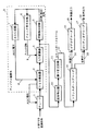
図1は、本発明の一実施形態に係るVSB受信機の構成を示すブロック図である。図1において、本発明の一実施形態に係るVSB受信機は、チューナ1と、ディジタル復調部2と、波形等化器10と、誤り訂正回路11と、トランスポートデコーダ13と、ビデオデコーダ16と、オーディオデコーダ17とで構成される。また、ディジタル復調部2は、VSB検波器3と、AD変換器4と、同期検出回路5と、クロック再生回路6と、AGC回路7とを備える。
【0080】
8値VSB変調された信号は、チューナ1に入力される。チューナ1は、8値VSB変調信号をIF信号に変換する。VSB検波器3は、IF信号に対して検波を行ってVSB復調する。AD変換器4は、VSB復調されたアナログ信号を8値のディジタルデータに変換して出力する。
このAD変換器4が出力するディジタルデータは、ATSC規格に準じた図2に示すフォーマットで構成されるデータであり、各セグメントの先頭にセグメント同期信号20が、各フィールドの先頭にフィールド同期信号21,22が存在し、1セグメントが832シンボルのデータで、1フィールドが313セグメントのデータで構成される。また、図3に、セグメント同期信号20およびフィールド同期信号21,22のデータ構成を示す。図3において、セグメント同期信号20は、−7〜+7で表現される8値データのうち、4シンボルデータがそれぞれ「+5,−5,−5,+5」となる特定パターンで構成される。また、フィールド同期信号21,22は、−5〜+5のレベル範囲で予め定められた特定パターンの828シンボルデータで構成される。
【0081】
同期検出回路5は、AD変換器4が出力するディジタルデータからセグメント同期信号20またはフィールド同期信号21,22を検出する。なお、同期検出回路5で行う同期信号の検出方法は、後述する実施形態において説明する。AGC回路7は、同期検出回路5が検出した同期信号に基づいて、セグメント同期信号20またはフィールド同期信号21,22のデータレベルが「−5〜+5」になるように、VSB検波器3に対してAGC電圧8をフィードバック制御する。クロック再生回路6は、同期検出回路5が検出した同期信号に基づいて、VSB受信機におけるクロック周波数が送信されてきたディジタルデータのクロック周波数と一致するように、AD変換器4に対してクロック信号9をフィードバック制御する。
【0082】
一方、AD変換器4で変換されたディジタルデータは、波形等化器10に出力される。波形等化器10は、伝送路等において生じた信号波形の歪み等を補正する(ゴースト妨害を除去する)。誤り訂正回路11は、歪み等が補正された信号波形に対して誤り訂正を行い、トランスポートストリーム12として出力する。トランスポートデコーダ13は、トランスポートストリーム12を任意のチャンネルの映像データ14と音声データ15とに分離する。ビデオデコーダ16は、分離された映像データ14を復号し、映像信号18として出力する。オーディオデコーダ17は、分離された音声データ15を復号し、音声信号19として出力する。
【0083】
次に、上記構成による本発明の一実施形態に係るVSB受信機において、ディジタル復調部2が取り得る構成に基づいて、本発明のVSB受信機のさらに詳細な説明を順に行う。
【0084】
(第1の実施形態)
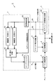
図4は、本発明の第1の実施形態に係るVSB受信機におけるディジタル復調部2の構成を示すブロック図である。図4において、第1の実施形態のディジタル復調部2は、VSB検波器3と、AD変換器4と、セグメント同期検出回路28と、利得検出器25と、増幅器26と、広帯域ループフィルタ32と、狭帯域ループフィルタ33と、切り換え回路34と、クロック再生回路6とを備える。
【0085】
図4に示すように、第1の実施形態のディジタル復調部2は、図1における同期検出回路5をセグメント同期検出回路28で構成し、AGC回路7を利得検出器25、増幅器26、広帯域ループフィルタ32、狭帯域ループフィルタ33および切り換え回路34で構成したものである。なお、図4において図1と同一の構成である部分については、同一の参照番号を付してその説明を省略する。
以下、第1の実施形態のディジタル復調部2の各構成を順に説明する。
【0086】
AD変換器4が出力するディジタルデータ(図2)は、波形等化器10およびセグメント同期検出回路28に入力される。セグメント同期検出回路28は、入力するディジタルデータに対してセグメント同期検出を行い、検出したセグメント同期信号20を利得検出器25へ、検出されたか否かの判定であるセグメント同期検出信号30を切り換え回路34へ出力する。
ここで、セグメント同期検出回路28が行うセグメント同期検出方法を、図5をさらに参照して説明する。図5は、セグメント同期検出回路28が行うセグメント同期検出の手順を示すフローチャートである。
【0087】
まず、セグメント同期検出回路28は、セグメント同期検出動作を開始するとセグメント同期検出信号30をローレベル“L”に初期化する(ステップS101)。次に、セグメント同期検出回路28は、符号が「+,−,−,+」のシンボルデータのパターンを検出したか否かを判断する(ステップS102)。ステップS102の判断でパターンを検出した場合、セグメント同期検出回路28は、セグメント同期検出信号30をハイレベル“H”にし、セグメント同期パターン検出回数Nを“1”に設定する(ステップS103)。そして、セグメント同期検出回路28は、ステップS102で初めて符号が「+,−,−,+」のシンボルデータのパターンを検出してから832シンボル後のデータの符号パターンが、同様に「+,−,−,+」であるか否かを判断する(ステップS104)。ステップS104の判断でパターンを検出した場合、セグメント同期検出回路28は、セグメント同期パターン検出回数Nの値を1つ増やす(ステップS106)。このステップS104およびS106の手順を、N=M(Mは、セグメント同期信号検出確定となるセグメント同期パターン検出回数であり、予め任意に定めてある)となるまで繰り返し、セグメント同期検出が確定する(ステップS107)。なお、ステップS104の判断でパターンを検出できなかった場合、セグメント同期検出回路28は、セグメント同期パターン検出回数Nをリセットして(ステップS105)、再度初めから「+,−,−,+」のシンボルデータの符号パターンの検出を始める。
【0088】
そして、セグメント同期パターン検出回数Nが値Mに達してセグメント同期信号検出が確定した後も、セグメント同期検出回路28は、引き続き832シンボル後のデータの符号パターンが「+,−,−,+」であるか否かを判断する(ステップS109)。ステップS109の判断でパターンを検出しなかった場合、セグメント同期検出回路28は、ステップS108で初期化したセグメント同期パターン未検出回数Lの値を1つ増やす(ステップS110)。このステップS109〜S110の手順を繰り返し、L=I(Iは、セグメント同期信号未検出確定となるセグメント同期パターン未検出回数であり、予め任意に定めてある)となった場合には、セグメント同期検出回路28は、セグメント同期検出が未確定に移行したと判断し、ステップS101に戻って再度セグメント同期検出確定への処理を行う(ステップS111)。
【0089】
利得検出器25は、AD変換器4が出力するディジタルデータのセグメント同期信号20のレベルが基準レベルである−5〜+5の値(ATSC規格で定められている)になるように、VSB検波器3の利得を制御する判定信号を、増幅器26へ出力する。具体的には、利得検出器25は、セグメント同期検出回路28で検出されたセグメント同期信号20のレベルが−5〜+5のレベルより小さい(例えば、−3〜+3)場合は、VSB検波器3の利得を上げる判定信号を、逆に大きい(例えば、−7〜+7)場合は、VSB検波器3の利得を下げる判定信号を出力する。
増幅器26は、利得検出器25が出力する判定信号を入力し、予め定めた増幅を行った後、広帯域ループフィルタ32および狭帯域ループフィルタ33へ出力する。
【0090】
広帯域ループフィルタ32は、AGC回路7におけるループ利得が大きく(AGCの追従性が良く)なるように、すなわち、セグメント同期信号20の検出時間の短縮をゴースト妨害除去性能よりも優先させた、フィルタ係数が設定されている。一方、狭帯域ループフィルタ33は、AGC回路7におけるループ利得が小さく(AGCの追従性が悪く)なるように、すなわち、ゴースト妨害除去性能をセグメント同期信号20の検出時間の短縮よりも優先させた、フィルタ係数が設定されている。
そして、増幅器26が出力する増幅後の判定信号は、広帯域ループフィルタ32および狭帯域ループフィルタ33をそれぞれ通過した後、切り換え回路34へ入力される。
【0091】
切り換え回路34は、広帯域ループフィルタ32および狭帯域ループフィルタ33をそれぞれ通過した信号と、セグメント同期検出回路28からセグメント同期検出信号30を入力する。そして、切り換え回路34は、セグメント同期検出信号30に従って、セグメント同期検出信号30が“L”である(セグメント同期信号20が検出されていない)場合には、広帯域ループフィルタ32を通過した信号を、セグメント同期検出信号30が“H”である(セグメント同期信号20が検出された)場合には、狭帯域ループフィルタ33を通過した信号を選択的に切り換え、AGC電圧8としてVSB検波器3へフィードバックする。
【0092】
ここで、具体的な実験による結果を示す。なお、この実験では、AGC回路7のループ利得の比率を、大きい場合:小さい場合=5:1に設定している。
ゴースト妨害のない信号に対して、AGC回路7のループ利得を大きくした場合のセグメント同期信号20の検出時間は0.35秒(20回測定した平均値、以下同じ)、AGC回路7のループ利得を小さくした場合のセグメント同期信号20の検出時間は0.31秒でほとんど差はない。一方、1μsec,D/U=6dBのゴースト妨害のある信号に対しては、AGC回路7のループ利得を大きくした場合のセグメント同期信号20の検出時間は4.5秒、AGC回路のループ利得を小さくした場合のセグメント同期信号20の検出時間は6.5秒と、ループ利得を大きくしたときの方がセグメント同期信号20の検出時間が短くなる。
また、ゴースト妨害除去の性能は、AGC回路7のループ利得を大きいままで固定した場合には、ゴースト妨害1μsecのゴースト除去性能はD/U=13dBであるが、セグメント同期信号20の検出前後においてAGC回路7のループ利得を大きい値から小さい値へと切り換えた場合には、ゴースト妨害1μsecの除去性能はD/U=8dBとなる。なお、Dは希望波(Desire)を、Uは妨害波(Undesire)を表し、D/Uが小さいほどゴースト妨害のレベルが大きくなる。
【0093】
以上のように、本発明の第1の実施形態に係るVSB受信機によれば、セグメント同期信号20を検出するまでは検出時間が短くなるようにループフィルタを広帯域に、セグメント同期信号20を検出した後はゴースト除去性能を向上させるためにループフィルタを狭帯域に切り換え、AGC回路7のループ利得を制御する。
これにより、受信信号にゴースト妨害のある場合でも、セグメント同期信号20の検出時間を短くすると共に、ゴースト妨害に対するゴースト除去性能をも向上させることが可能となる。
【0094】
(第2の実施形態)
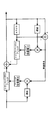
図6は、本発明の第2の実施形態に係るVSB受信機におけるディジタル復調部2の構成を示すブロック図である。図6において、第2の実施形態のディジタル復調部2は、VSB検波器3と、AD変換器4と、セグメント同期検出回路28と、利得検出器25と、増幅器26と、DA変換器29と、抵抗35〜37と、コンデンサ38,39と、スイッチダイオード40と、クロック再生回路6とを備える。
【0095】
図6に示すように、第2の実施形態のディジタル復調部2は、図1における同期検出回路5をセグメント同期検出回路28で構成し、AGC回路7を利得検出器25、増幅器26、DA変換器29および抵抗35〜37、コンデンサ38,39,スイッチダイオード40からなるディスクリート回路で構成したものである。なお、図6において図1および図4と同一の構成である部分については、同一の参照番号を付してその説明を省略する。
以下、第2の実施形態のディジタル復調部2の各構成を順に説明する。
【0096】
DA変換器29は、増幅器26が出力する増幅後のディジタルの判定信号を入力し、アナログの判定信号に変換して出力する。このDA変換器29の出力信号は、ディスクリート回路の抵抗35の一方端子に入力される。抵抗35の他方端子は、抵抗36の一方端子と接続されると共に、VSB検波器3にフィードバック出力される。抵抗36の他方端子は、コンデンサ38およびコンデンサ39の一方端子とそれぞれ接続される。コンデンサ38の他方端子は、スイッチダイオード40のアノード端子と抵抗37の一方端子とに接続される。コンデンサ39の他方端子およびスイッチダイオード40のカソード端子は、それぞれ接地される。抵抗37の他方端子には、セグメント同期検出回路28が出力するセグメント同期検出信号30が入力される。
【0097】
まず、セグメント同期信号20が検出されるまでは、セグメント同期検出信号30が“L”であるので、スイッチダイオード40がオフとなる。従って、この場合、ディスクリート回路は、抵抗35,36およびコンデンサ39で構成される広帯域ループフィルタとして機能する。
次に、セグメント同期信号20が検出された後は、セグメント同期検出信号30が“H”となるので、スイッチダイオード40がオンとなる。従って、この場合、ディスクリート回路は、抵抗35,36およびコンデンサ38,39で構成される狭帯域ループフィルタとして機能する。
【0098】
よって、抵抗35の他方端子からVSB検波器3へフィードバックされるAGC電圧8は、セグメント同期信号20が検出されていない場合には、広帯域ループフィルタを通過したAGC電圧8が、セグメント同期信号20が検出された場合には、狭帯域ループフィルタを通過したAGC電圧8が、セグメント同期検出信号30に従って選択的に切り換えられて出力される。
【0099】
以上のように、本発明の第2の実施形態に係るVSB受信機によれば、セグメント同期信号20を検出するまでは検出時間が短くなるようにループフィルタを広帯域に、セグメント同期信号20を検出した後はゴースト除去性能を向上させるためにループフィルタを狭帯域に切り換え、AGC回路7のループ利得を制御する。
これにより、受信信号にゴースト妨害のある場合でも、セグメント同期信号20の検出時間を短くすると共に、ゴースト妨害に対するゴースト除去性能をも向上させることが可能となる。
【0100】
(第3の実施形態)
図7は、本発明の第3の実施形態に係るVSB受信機におけるディジタル復調部2の構成を示すブロック図である。図7において、第3の実施形態のディジタル復調部2は、VSB検波器3と、AD変換器4と、セグメント同期検出回路28と、利得検出器25と、増幅器26と、ディジタルフィルタ42と、切り換え回路34と、広帯域の係数43と、狭帯域の係数44と、DA変換器29と、クロック再生回路6とを備える。
【0101】
図7に示すように、第3の実施形態のディジタル復調部2は、図1における同期検出回路5をセグメント同期検出回路28で構成し、AGC回路7を利得検出器25、増幅器26、ディジタルフィルタ42、切り換え回路34、広帯域の係数43、狭帯域の係数44およびDA変換器29で構成したものである。なお、図7において図1および図4と同一の構成である部分については、同一の参照番号を付してその説明を省略する。
以下、第3の実施形態のディジタル復調部2の各構成を順に説明する。
【0102】
増幅器26が出力する増幅後のディジタルの判定信号は、ディジタルフィルタ42においてフィルタリングされ、DA変換器29でアナログのAGC電圧8に変換された後、VSB検波器3にフィードバックされる。
広帯域の係数43には、ディジタルフィルタ42を広帯域で機能させるために必要なフィルタ係数が格納されている。また、狭帯域の係数44には、ディジタルフィルタ42を狭帯域で機能させるために必要なフィルタ係数が格納されている。
そして、切り換え回路34は、セグメント同期検出信号30に従って、セグメント同期検出信号30が“L”である(セグメント同期信号20が検出されていない)場合には、広帯域の係数43をディジタルフィルタ42に書き込み、セグメント同期検出信号30が“H”である(セグメント同期信号20が検出された)場合には、狭帯域の係数44をディジタルフィルタ42に書き込む。
【0103】
よって、ディジタルフィルタ42は、セグメント同期信号20が検出されていない場合には、広帯域ループフィルタとして機能し、セグメント同期信号20が検出された場合には、狭帯域ループフィルタとして機能するため、VSB検波器3へフィードバックされるAGC電圧8は、セグメント同期検出信号30に従って帯域が選択的に切り換えられて出力される。
【0104】
以上のように、本発明の第3の実施形態に係るVSB受信機によれば、セグメント同期信号20を検出するまでは検出時間が短くなるようにループフィルタを広帯域に、セグメント同期信号20を検出した後はゴースト除去性能を向上させるためにループフィルタを狭帯域に切り換え、AGC回路7のループ利得を制御する。
これにより、受信信号にゴースト妨害のある場合でも、セグメント同期信号20の検出時間を短くすると共に、ゴースト妨害に対するゴースト除去性能をも向上させることが可能となる。
【0105】
(第4の実施形態)
図8は、本発明の第4の実施形態に係るVSB受信機におけるディジタル復調部2の構成を示すブロック図である。図8において、第4の実施形態のディジタル復調部2は、VSB検波器3と、AD変換器4と、セグメント同期検出回路28と、利得検出器25と、増幅器(利得大)52と、増幅器(利得小)53と、切り換え回路34と、ループフィルタ54と、クロック再生回路6とを備える。
【0106】
図8に示すように、第4の実施形態のディジタル復調部2は、図1における同期検出回路5をセグメント同期検出回路28で構成し、AGC回路7を利得検出器25、増幅器(利得大)52、増幅器(利得小)53、切り換え回路34およびループフィルタ54で構成したものである。なお、図8において図1および図4と同一の構成である部分については、同一の参照番号を付してその説明を省略する。
以下、第4の実施形態のディジタル復調部2の各構成を順に説明する。
【0107】
利得検出器25が出力する判定信号は、増幅器(利得大)52および増幅器(利得小)53にそれぞれ入力される。
増幅器(利得大)52は、AGC回路7におけるループ利得が大きく(AGCの追従性が良く)なるように、すなわち、セグメント同期信号20の検出時間の短縮をゴースト妨害除去性能よりも優先させた、増幅利得値が設定されている。一方、増幅器(利得小)53は、AGC回路7におけるループ利得が小さく(AGCの追従性が悪く)なるように、すなわち、ゴースト妨害除去性能をセグメント同期信号20の検出時間の短縮よりも優先させた、増幅利得値が設定されている。
このように、利得検出器25が出力する判定信号は、増幅器(利得大)52および増幅器(利得小)53でそれぞれ増幅された後、切り換え回路34へ入力される。
【0108】
切り換え回路34は、増幅器(利得大)52および増幅器(利得小)53でそれぞれ増幅された信号と、セグメント同期検出回路28からセグメント同期検出信号30を入力する。そして、切り換え回路34は、セグメント同期検出信号30に従って、セグメント同期検出信号30が“L”である(セグメント同期信号20が検出されていない)場合には、増幅器(利得大)52で増幅された信号を、セグメント同期検出信号30が“H”である(セグメント同期信号20が検出された)場合には、増幅器(利得小)53で増幅された信号を選択的に切り換えて出力する。そして、切り換え回路34から選択的に出力された信号は、ループフィルタ54を介した後、AGC電圧8としてVSB検波器3へフィードバックされる。
【0109】
以上のように、本発明の第4の実施形態に係るVSB受信機によれば、セグメント同期信号20を検出するまでは検出時間が短くなるように増幅利得を大きい値に、セグメント同期信号20を検出した後はゴースト除去性能を向上させるために増幅利得を小さい値に切り換え、AGC回路7のループ利得を制御する。
これにより、受信信号にゴースト妨害のある場合でも、セグメント同期信号20の検出時間を短くすると共に、ゴースト妨害に対するゴースト除去性能をも向上させることが可能となる。
【0110】
(第5の実施形態)
図9は、本発明の第5の実施形態に係るVSB受信機におけるディジタル復調部2の構成を示すブロック図である。図9において、第5の実施形態のディジタル復調部2は、VSB検波器3と、AD変換器4と、セグメント同期検出回路28と、利得検出器25と、DA変換器29と、オペアンプ(利得大)55と、オペアンプ(利得小)56と、切り換え回路34と、ループフィルタ54と、クロック再生回路6とを備える。
【0111】
図9に示すように、第5の実施形態のディジタル復調部2は、図1における同期検出回路5をセグメント同期検出回路28で構成し、AGC回路7を利得検出器25、DA変換器29、オペアンプ(利得大)55、オペアンプ(利得小)56、切り換え回路34およびループフィルタ54で構成したものである。なお、図9において図1および図4と同一の構成である部分については、同一の参照番号を付してその説明を省略する。
以下、第5の実施形態のディジタル復調部2の各構成を順に説明する。
【0112】
DA変換器29は、利得検出器25が出力するディジタルの判定信号を入力し、アナログの判定信号に変換して出力する。このアナログの判定信号は、オペアンプ(利得大)55およびオペアンプ(利得小)56にそれぞれ入力される。
オペアンプ(利得大)55は、AGC回路7におけるループ利得が大きく(AGCの追従性が良く)なるように、すなわち、セグメント同期信号20の検出時間の短縮をゴースト妨害除去性能よりも優先させた、増幅利得値が設定されている。一方、オペアンプ(利得小)56は、AGC回路7におけるループ利得が小さく(AGCの追従性が悪く)なるように、すなわち、ゴースト妨害除去性能をセグメント同期信号20の検出時間の短縮よりも優先させた、増幅利得値が設定されている。
このように、DA変換器29が出力するアナログの判定信号は、オペアンプ(利得大)55およびオペアンプ(利得小)56でそれぞれ増幅された後、切り換え回路34へ入力される。
【0113】
切り換え回路34は、オペアンプ(利得大)55およびオペアンプ(利得小)56でそれぞれ増幅された信号と、セグメント同期検出回路28からセグメント同期検出信号30を入力する。そして、切り換え回路34は、セグメント同期検出信号30に従って、セグメント同期検出信号30が“L”である(セグメント同期信号20が検出されていない)場合には、オペアンプ(利得大)55で増幅された信号を、セグメント同期検出信号30が“H”である(セグメント同期信号20が検出された)場合には、オペアンプ(利得小)56で増幅された信号を選択的に切り換えて出力する。そして、切り換え回路34から選択的に出力された信号は、ループフィルタ54を介した後、AGC電圧8としてVSB検波器3へフィードバックされる。
【0114】
以上のように、本発明の第5の実施形態に係るVSB受信機によれば、セグメント同期信号20を検出するまでは検出時間が短くなるように増幅利得を大きい値に、セグメント同期信号20を検出した後はゴースト除去性能を向上させるために増幅利得を小さい値に切り換え、AGC回路7のループ利得を制御する。
これにより、受信信号にゴースト妨害のある場合でも、セグメント同期信号20の検出時間を短くすると共に、ゴースト妨害に対するゴースト除去性能をも向上させることが可能となる。
【0115】
(第6の実施形態)
図10は、本発明の第6の実施形態に係るVSB受信機におけるディジタル復調部2の構成を示すブロック図である。図10において、第6の実施形態のディジタル復調部2は、VSB検波器3と、AD変換器4と、セグメント同期検出回路28と、利得検出器25と、乗算器57と、係数大58と、係数小59と、切り換え回路34と、DA変換器29と、ループフィルタ54と、クロック再生回路6とを備える。
【0116】
図10に示すように、第6の実施形態のディジタル復調部2は、図1における同期検出回路5をセグメント同期検出回路28で構成し、AGC回路7を利得検出器25、乗算器57と、係数大58と、係数小59と、切り換え回路34と、DA変換器29およびループフィルタ54で構成したものである。なお、図10において図1および図4と同一の構成である部分については、同一の参照番号を付してその説明を省略する。
以下、第6の実施形態のディジタル復調部2の各構成を順に説明する。
【0117】
利得検出器25が出力するディジタルの判定信号は、乗算器57において増幅され、DA変換器29でアナログのAGC電圧8に変換された後、VSB検波器3にフィードバックされる。
係数大58には、乗算器57の増幅利得を大きくするために必要な係数が格納されている。また、係数小59には、乗算器57の増幅利得を小さくするために必要な係数が格納されている。
そして、切り換え回路34は、セグメント同期検出信号30に従って、セグメント同期検出信号30が“L”である(セグメント同期信号20が検出されていない)場合には、係数大58を乗算器57に入力し、セグメント同期検出信号30が“H”である(セグメント同期信号20が検出された)場合には、係数小59を乗算器57に入力する。
【0118】
よって、乗算器57は、セグメント同期信号20が検出されていない場合には利得大の増幅器として機能し、セグメント同期信号20が検出された場合には利得小の増幅器として機能するため、VSB検波器3へフィードバックされるAGC電圧8は、セグメント同期検出信号30に従って利得値が選択的に切り換えられて出力される。
【0119】
以上のように、本発明の第6の実施形態に係るVSB受信機によれば、セグメント同期信号20を検出するまでは検出時間が短くなるように増幅利得を大きい値に、セグメント同期信号20を検出した後はゴースト除去性能を向上させるために増幅利得を小さい値に切り換え、AGC回路7のループ利得を制御する。
これにより、受信信号にゴースト妨害のある場合でも、セグメント同期信号20の検出時間を短くすると共に、ゴースト妨害に対するゴースト除去性能をも向上させることが可能となる。
【0120】
(第7の実施形態)
上記第1〜第6の実施形態においては、AGC回路7のループ利得を切り換えることで、セグメント同期信号20の検出時間を短くすると共に、ゴースト妨害に対するゴースト除去性能をも向上させるVSB受信機を説明した。
次に、以下の実施形態においては、クロック再生回路6のループ利得をも切り換えることで、さらにセグメント同期信号20の検出時間を短くすると共に、ゴースト妨害時においても正確なクロック再生を行うことができるVSB受信機を説明する。
【0121】
図11は、本発明の第7の実施形態に係るVSB受信機におけるディジタル復調部2の構成を示すブロック図である。図11において、第7の実施形態のディジタル復調部2は、VSB検波器3と、AD変換器4と、セグメント同期検出回路28と、クロック周波数検出器60と、増幅器61と、広帯域ループフィルタ62と、狭帯域ループフィルタ63と、切り換え回路64と、可変クロック発振器65と、AGC回路7とを備える。
【0122】
図11に示すように、第7の実施形態のディジタル復調部2は、図1における同期検出回路5をセグメント同期検出回路28で構成し、クロック再生回路6をクロック周波数検出器60、増幅器61、広帯域ループフィルタ62、狭帯域ループフィルタ63、切り換え回路64および可変クロック発振器65で構成したものである。なお、図11において図1および図4と同一の構成である部分については、同一の参照番号を付してその説明を省略する。また、図11におけるAGC回路7には、上記第1〜第6の実施形態のいずれかの構成が用いられる。
以下、第7の実施形態のディジタル復調部2の各構成を順に説明する。
【0123】
AD変換器4が出力するディジタルデータ(図2)は、波形等化器10およびセグメント同期検出回路28に入力される。セグメント同期検出回路28は、入力するディジタルデータに対してセグメント同期検出を行い、検出したセグメント同期信号20をクロック周波数検出器60へ、検出されたか否かの判定であるセグメント同期検出信号30を切り換え回路64へ出力する。
なお、セグメント同期検出回路28が行うセグメント同期検出方法は、上記第1の実施形態で述べたので、ここでの詳細な説明は省略する。
【0124】
クロック周波数検出器60は、VSB受信機のクロック信号9の周波数が送信されてきたデータのクロック周波数より高いか低いかを判定し、その判定信号を増幅器61へ出力する。
ここで、クロック周波数検出器60が行うクロック周波数の判定方法を、図12をさらに参照して説明する。図12は、クロック周波数検出器60が行うクロック周波数の判定方法の概念を説明する図である。
【0125】
前提として、AD変換器4に入力される信号は帯域制限されているため、実際のセグメント同期信号20は、図3に示したような4シンボルが「+5,−5,−5,+5」の矩形波ではなく、図12に示すような波形となる。
まず、VSB受信機のクロック信号9が送信データのクロック周波数より高い場合(図12(a))、AD変換器4においてVSB受信機のクロック信号9の立ち上がりタイミングでセグメント同期信号20の「−5,−5」のシンボルデータを変換すると、それぞれd1,d2(d1>d2)のディジタルデータに変換される。逆に、VSB受信機のクロック信号9が送信データのクロック周波数より低い場合(図12(b))、AD変換器4においてVSB受信機のクロック信号9の立ち上がりタイミングでセグメント同期信号20の「−5,−5」のシンボルデータを変換すると、それぞれd1,d2(d1<d2)のディジタルデータに変換される。
【0126】
そこで、クロック周波数検出器60は、この2つのデータ差(d1>d2またはd1<d2)を判断し、AD変換器4の出力において2つのデータ差がなくなる(d1=d2)クロック信号9が可変クロック発振器65から出力されるように判定信号を出力する。
この処理によって、VSB受信機のクロック信号9と送信データのクロック周波数が一致した場合(図12(c))には、AD変換器4においてVSB受信機のクロック信号9の立ち上がりタイミングでセグメント同期信号20の「−5,−5」のシンボルデータを変換すると、それぞれ同じ値のd1,d2(d1=d2)のディジタルデータに変換されるように制御される。
増幅器61は、クロック周波数検出器60が出力する判定信号を入力し、予め定めた増幅を行った後、広帯域ループフィルタ62および狭帯域ループフィルタ63へ出力する。
【0127】
広帯域ループフィルタ62は、クロック再生回路6におけるループ利得が大きく(クロック再生の追従性が良く)なるように、すなわち、セグメント同期信号20の検出時間の短縮を正確なクロック再生(換言すれば、ゴースト妨害除去性能)よりも優先させた、フィルタ係数が設定されている。一方、狭帯域ループフィルタ63は、クロック再生回路6におけるループ利得が小さく(クロック再生の追従性が悪く)なるように、すなわち、正確なクロック再生をセグメント同期信号20の検出時間の短縮よりも優先させた、フィルタ係数が設定されている。そして、増幅器61が出力する増幅後の判定信号は、広帯域ループフィルタ62および狭帯域ループフィルタ63をそれぞれ通過した後、切り換え回路64へ入力される。
【0128】
切り換え回路64は、広帯域ループフィルタ62および狭帯域ループフィルタ63をそれぞれ通過した信号と、セグメント同期検出回路28からセグメント同期検出信号30を入力する。そして、切り換え回路64は、セグメント同期検出信号30に従って、セグメント同期検出信号30が“L”である(セグメント同期信号20が検出されていない)場合には、広帯域ループフィルタ62を通過した信号を、セグメント同期検出信号30が“H”である(セグメント同期信号20が検出された)場合には、狭帯域ループフィルタ63を通過した信号(DC電圧)を選択的に切り換え、可変クロック発振器65へ出力する。
可変クロック発振器65は、切り換え回路64が出力する信号(DC電圧)に基づいて発振するクロック信号9の周波数を可変し、AD変換器4に対してフィードバック出力する。
【0129】
以上のように、本発明の第7の実施形態に係るVSB受信機によれば、AGC回路7のループ利得の制御に加え、セグメント同期信号20を検出するまでは検出時間が短くなるようにループフィルタを広帯域に、セグメント同期信号20を検出した後は正確なクロック再生を行う(すなわち、ゴースト除去性能を向上させる)ためにループフィルタを狭帯域に切り換え、クロック再生回路6のループ利得を制御する。
これにより、受信信号にゴースト妨害のある場合でも、セグメント同期信号20の検出時間を短くすると共に、ゴースト妨害に対するゴースト除去性能をも向上させることが可能となり、さらに、VSB受信機の再生クロックにジッタが生じなくなるので、受信信号に誤りが発生しなくなる。
【0130】
(第8の実施形態)
図13は、本発明の第8の実施形態に係るVSB受信機におけるディジタル復調部2の構成を示すブロック図である。図13において、第8の実施形態のディジタル復調部2は、VSB検波器3と、AD変換器4と、セグメント同期検出回路28と、クロック周波数検出器60と、増幅器61と、DA変換器69と、抵抗75〜77と、コンデンサ78,79と、スイッチダイオード80と、可変クロック発振器65と、AGC回路7とを備える。
【0131】
図13に示すように、第8の実施形態のディジタル復調部2は、図1における同期検出回路5をセグメント同期検出回路28で構成し、クロック再生回路6をクロック周波数検出器60、増幅器61、DA変換器69、抵抗75〜77、コンデンサ78,79,スイッチダイオード80からなるディスクリート回路および可変クロック発振器65で構成したものである。なお、図13において図1、図4および図11と同一の構成である部分については、同一の参照番号を付してその説明を省略する。また、図13におけるAGC回路7には、上記第1〜第6の実施形態のいずれかの構成が用いられる。
以下、第8の実施形態のディジタル復調部2の各構成を順に説明する。
【0132】
DA変換器69は、増幅器61が出力する増幅後のディジタルの判定信号を入力し、アナログの判定信号に変換して出力する。このDA変換器69の出力信号は、ディスクリート回路の抵抗75の一方端子に入力される。抵抗75の他方端子は、抵抗76の一方端子と接続されると共に、可変クロック発振器65に出力される。抵抗76の他方端子は、コンデンサ78およびコンデンサ79の一方端子とそれぞれ接続される。コンデンサ78の他方端子は、スイッチダイオード80のアノード端子と抵抗77の一方端子とに接続される。コンデンサ79の他方端子およびスイッチダイオード80のカソード端子は、それぞれ接地される。抵抗77の他方端子には、セグメント同期検出回路28が出力するセグメント同期検出信号30が入力される。
【0133】
まず、セグメント同期信号20が検出されるまでは、セグメント同期検出信号30が“L”であるので、スイッチダイオード80がオフとなる。従って、この場合、ディスクリート回路は、抵抗75,76およびコンデンサ79で構成される広帯域ループフィルタとして機能する。
次に、セグメント同期信号20が検出された後は、セグメント同期検出信号30が“H”となるので、スイッチダイオード80がオンとなる。従って、この場合、ディスクリート回路は、抵抗75,76およびコンデンサ78,79で構成される狭帯域ループフィルタとして機能する。
【0134】
よって、抵抗75の他方端子から可変クロック発振器65を介してAD変換器4へフィードバックされるクロック信号9は、セグメント同期信号20が検出されていない場合には、広帯域ループフィルタを通過した判定信号が、セグメント同期信号20が検出された場合には、狭帯域ループフィルタを通過した判定信号が、セグメント同期検出信号30に従って選択的に切り換えられて出力される。
【0135】
ここで、具体的な実験による結果を示す。なお、各素子の値は、抵抗35が18kΩ、抵抗36が1kΩ、コンデンサ38が1μF、コンデンサ39が3.3μFである。
セグメント同期信号20の検出前後でループフィルタの切り換えを行わずに、抵抗75,76およびコンデンサ79のみで広帯域ループフィルタを構成した場合のセグメント同期信号20の検出時間は1.05秒(20回測定した平均値、以下同じ)、セグメント同期信号20の検出前後でループフィルタの帯域切り換えを行った場合のセグメント同期信号20の検出時間は0.36秒となった。
また、ゴースト妨害除去の性能は、クロック再生回路6のループを広帯域で固定した場合(すなわち、AGC回路7のループ利得を切り換えるだけの場合)には、ゴースト妨害1μsecのゴースト除去の性能はD/U=8dBであるが、セグメント同期信号20の検出前後においてクロック再生回路6のループフィルタの帯域を広帯域から狭帯域へと切り換えた場合には、ゴースト妨害1μsecのゴースト除去性能は、D/U=6dBへとさらに改善される。
【0136】
以上のように、本発明の第8の実施形態に係るVSB受信機によれば、AGC回路7のループ利得の制御に加え、セグメント同期信号20を検出するまでは検出時間が短くなるようにループフィルタを広帯域に、セグメント同期信号20を検出した後は正確なクロック再生を行う(すなわち、ゴースト除去性能を向上させる)ためにループフィルタを狭帯域に切り換え、クロック再生回路6のループ利得を制御する。
これにより、受信信号にゴースト妨害のある場合でも、セグメント同期信号20の検出時間を短くすると共に、ゴースト妨害に対するゴースト除去性能をも向上させることが可能となり、さらに、VSB受信機の再生クロックにジッタが生じなくなるので、受信信号に誤りが発生しなくなる。
【0137】
(第9の実施形態)
図14は、本発明の第9の実施形態に係るVSB受信機におけるディジタル復調部2の構成を示すブロック図である。図14において、第9の実施形態のディジタル復調部2は、VSB検波器3と、AD変換器4と、セグメント同期検出回路28と、クロック周波数検出器60と、増幅器61と、ディジタルフィルタ82と、切り換え回路64と、広帯域の係数83と、狭帯域の係数84と、DA変換器69と、可変クロック発振器65と、AGC回路7とを備える。
【0138】
図14に示すように、第9の実施形態のディジタル復調部2は、図1における同期検出回路5をセグメント同期検出回路28で構成し、クロック再生回路6をクロック周波数検出器60、増幅器61、ディジタルフィルタ82、切り換え回路64、広帯域の係数83、狭帯域の係数84、DA変換器69および可変クロック発振器65で構成したものである。なお、図14において図1,図4および図11と同一の構成である部分については、同一の参照番号を付してその説明を省略する。また、図14におけるAGC回路7には、上記第1〜第6の実施形態のいずれかの構成が用いられる。
以下、第9の実施形態のディジタル復調部2の各構成を順に説明する。
【0139】
増幅器61が出力する増幅後のディジタルの判定信号は、ディジタルフィルタ82においてフィルタリングされ、DA変換器69でアナログ信号(DC電圧)に変換された後、可変クロック発振器65を介してクロック信号9としてAD変換器4にフィードバックされる。
広帯域の係数83には、ディジタルフィルタ82を広帯域で機能させるために必要なフィルタ係数が格納されている。また、狭帯域の係数84には、ディジタルフィルタ82を狭帯域で機能させるために必要なフィルタ係数が格納されている。
そして、切り換え回路64は、セグメント同期検出信号30に従って、セグメント同期検出信号30が“L”である(セグメント同期信号20が検出されていない)場合には、広帯域の係数83をディジタルフィルタ82に書き込み、セグメント同期検出信号30が“H”である(セグメント同期信号20が検出された)場合には、狭帯域の係数84をディジタルフィルタ82に書き込む。
【0140】
よって、ディジタルフィルタ82は、セグメント同期信号20が検出されていない場合には、広帯域ループフィルタとして機能し、セグメント同期信号20が検出された場合には、狭帯域ループフィルタとして機能するため、AD変換器4へフィードバックされるクロック信号9は、セグメント同期検出信号30に従って帯域が選択的に切り換えられて出力される。
【0141】
以上のように、本発明の第9の実施形態に係るVSB受信機によれば、AGC回路7のループ利得の制御に加え、セグメント同期信号20を検出するまでは検出時間が短くなるようにループフィルタを広帯域に、セグメント同期信号20を検出した後は正確なクロック再生を行う(すなわち、ゴースト除去性能を向上させる)ためにループフィルタを狭帯域に切り換え、クロック再生回路6のループ利得を制御する。
これにより、受信信号にゴースト妨害のある場合でも、セグメント同期信号20の検出時間を短くすると共に、ゴースト妨害に対するゴースト除去性能をも向上させることが可能となり、さらに、VSB受信機の再生クロックにジッタが生じなくなるので、受信信号に誤りが発生しなくなる。
【0142】
(第10の実施形態)
図15は、本発明の第10の実施形態に係るVSB受信機におけるディジタル復調部2の構成を示すブロック図である。図15において、第10の実施形態のディジタル復調部2は、VSB検波器3と、AD変換器4と、セグメント同期検出回路28と、クロック周波数検出器60と、増幅器(利得大)92と、増幅器(利得小)93と、切り換え回路64と、ループフィルタ94と、可変クロック発振器65と、AGC回路7とを備える。
【0143】
図15に示すように、第10の実施形態のディジタル復調部2は、図1における同期検出回路5をセグメント同期検出回路28で構成し、クロック再生回路6をクロック周波数検出器60、増幅器(利得大)92、増幅器(利得小)93、切り換え回路64、ループフィルタ94および可変クロック発振器65で構成したものである。なお、図15において図1、図4および図11と同一の構成である部分については、同一の参照番号を付してその説明を省略する。また、図15におけるAGC回路7には、上記第1〜第6の実施形態のいずれかの構成が用いられる。
以下、第10の実施形態のディジタル復調部2の各構成を順に説明する。
【0144】
クロック周波数検出器60が出力する判定信号は、増幅器(利得大)92および増幅器(利得小)93にそれぞれ入力される。
増幅器(利得大)92は、クロック再生回路6におけるループ利得が大きく(クロック再生の追従性が良く)なるように、すなわち、セグメント同期信号20の検出時間の短縮を正確なクロック再生(換言すれば、ゴースト妨害除去性能)よりも優先させた、増幅利得値が設定されている。一方、増幅器(利得小)93は、クロック再生回路6におけるループ利得が小さく(クロック再生の追従性が悪く)なるように、すなわち、正確なクロック再生をセグメント同期信号20の検出時間の短縮よりも優先させた、増幅利得値が設定されている。
このように、クロック周波数検出器60が出力する判定信号は、増幅器(利得大)92および増幅器(利得小)93でそれぞれ増幅された後、切り換え回路64へ入力される。
【0145】
切り換え回路64は、増幅器(利得大)92および増幅器(利得小)93でそれぞれ増幅された信号と、セグメント同期検出回路28からセグメント同期検出信号30を入力する。そして、切り換え回路64は、セグメント同期検出信号30に従って、セグメント同期検出信号30が“L”である(セグメント同期信号20が検出されていない)場合には、増幅器(利得大)92で増幅された信号を、セグメント同期検出信号30が“H”である(セグメント同期信号20が検出された)場合には、増幅器(利得小)93で増幅された信号を選択的に切り換えて出力する。そして、切り換え回路64から選択的に出力された信号(DC電圧)は、ループフィルタ94および可変クロック発振器65を介した後、クロック信号9としてAD変換器4へフィードバックされる。
【0146】
以上のように、本発明の第10の実施形態に係るVSB受信機によれば、AGC回路7のループ利得の制御に加え、セグメント同期信号20を検出するまでは検出時間が短くなるように増幅利得を大きい値に、セグメント同期信号20を検出した後は正確なクロック再生を行う(すなわち、ゴースト除去性能を向上させる)ために増幅利得を小さい値に切り換え、クロック再生回路6のループ利得を制御する。
これにより、受信信号にゴースト妨害のある場合でも、セグメント同期信号20の検出時間を短くすると共に、ゴースト妨害に対するゴースト除去性能をも向上させることが可能となり、さらに、VSB受信機の再生クロックにジッタが生じなくなるので、受信信号に誤りが発生しなくなる。
【0147】
(第11の実施形態)
図16は、本発明の第11の実施形態に係るVSB受信機におけるディジタル復調部2の構成を示すブロック図である。図16において、第11の実施形態のディジタル復調部2は、VSB検波器3と、AD変換器4と、セグメント同期検出回路28と、クロック周波数検出器60と、DA変換器69と、オペアンプ(利得大)95と、オペアンプ(利得小)96と、切り換え回路64と、ループフィルタ94と、可変クロック発振器65と、AGC回路7とを備える。
【0148】
図16に示すように、第11の実施形態のディジタル復調部2は、図1における同期検出回路5をセグメント同期検出回路28で構成し、クロック再生回路6をクロック周波数検出器60、DA変換器69、オペアンプ(利得大)95、オペアンプ(利得小)96、切り換え回路64、ループフィルタ94および可変クロック発振器65で構成したものである。なお、図16において図1、図4および図11と同一の構成である部分については、同一の参照番号を付してその説明を省略する。また、図16におけるAGC回路7には、上記第1〜第6の実施形態のいずれかの構成が用いられる。
以下、第11の実施形態のディジタル復調部2の各構成を順に説明する。
【0149】
DA変換器69は、クロック周波数検出器60が出力するディジタルの判定信号を入力し、アナログの判定信号に変換して出力する。このアナログの判定信号は、オペアンプ(利得大)95およびオペアンプ(利得小)96にそれぞれ入力される。
オペアンプ(利得大)95は、クロック再生回路6におけるループ利得が大きく(クロック再生の追従性が良く)なるように、すなわち、セグメント同期信号20の検出時間の短縮を正確なクロック再生(換言すれば、ゴースト妨害除去性能)よりも優先させた、増幅利得値が設定されている。一方、オペアンプ(利得小)96は、クロック再生回路6におけるループ利得が小さく(クロック再生の追従性が悪く)なるように、すなわち、正確なクロック再生をセグメント同期信号20の検出時間の短縮よりも優先させた、増幅利得値が設定されている。
このように、DA変換器69が出力するアナログの判定信号は、オペアンプ(利得大)95およびオペアンプ(利得小)96でそれぞれ増幅された後、切り換え回路64へ入力される。
【0150】
切り換え回路64は、オペアンプ(利得大)95およびオペアンプ(利得小)96でそれぞれ増幅された信号と、セグメント同期検出回路28からセグメント同期検出信号30を入力する。そして、切り換え回路64は、セグメント同期検出信号30に従って、セグメント同期検出信号30が“L”である(セグメント同期信号20が検出されていない)場合には、オペアンプ(利得大)95で増幅された信号を、セグメント同期検出信号30が“H”である(セグメント同期信号20が検出された)場合には、オペアンプ(利得小)96で増幅された信号を選択的に切り換えて出力する。そして、切り換え回路64から選択的に出力された信号は、ループフィルタ94および可変クロック発振器65を介した後、クロック信号9としてAD変換器4へフィードバックされる。
【0151】
以上のように、本発明の第11の実施形態に係るVSB受信機によれば、AGC回路7のループ利得の制御に加え、セグメント同期信号20を検出するまでは検出時間が短くなるように増幅利得を大きい値に、セグメント同期信号20を検出した後は正確なクロック再生を行う(すなわち、ゴースト除去性能を向上させる)ために増幅利得を小さい値に切り換え、クロック再生回路6のループ利得を制御する。
これにより、受信信号にゴースト妨害のある場合でも、セグメント同期信号20の検出時間を短くすると共に、ゴースト妨害に対するゴースト除去性能をも向上させることが可能となり、さらに、VSB受信機の再生クロックにジッタが生じなくなるので、受信信号に誤りが発生しなくなる。
【0152】
(第12の実施形態)
図17は、本発明の第12の実施形態に係るVSB受信機におけるディジタル復調部2の構成を示すブロック図である。図17において、第12の実施形態のディジタル復調部2は、VSB検波器3と、AD変換器4と、セグメント同期検出回路28と、クロック周波数検出器60と、乗算器97と、係数大98と、係数小99と、切り換え回路64と、DA変換器69と、ループフィルタ94と、可変クロック発振器65と、AGC回路7とを備える。
【0153】
図17に示すように、第12の実施形態のディジタル復調部2は、図1における同期検出回路5をセグメント同期検出回路28で構成し、クロック再生回路6をクロック周波数検出器60、乗算器97、係数大98、係数小99、切り換え回路64、DA変換器69、ループフィルタ94および可変クロック発振器65で構成したものである。なお、図17において図1、図4および図11と同一の構成である部分については、同一の参照番号を付してその説明を省略する。また、図17におけるAGC回路7には、上記第1〜第6の実施形態のいずれかの構成が用いられる。
以下、第12の実施形態のディジタル復調部2の各構成を順に説明する。
【0154】
クロック周波数検出器60が出力するディジタルの判定信号は、乗算器97において増幅され、DA変換器69でアナログのDC電圧に変換された後、ループフィルタ94および可変クロック発振器65を介してAD変換器4にフィードバックされる。
係数大98には、乗算器97の増幅利得を大きくするために必要な係数が格納されている。また、係数小99には、乗算器97の増幅利得を小さくするために必要な係数が格納されている。
そして、切り換え回路64は、セグメント同期検出信号30に従って、セグメント同期検出信号30が“L”である(セグメント同期信号20が検出されていない)場合には、係数大98を乗算器97に入力し、セグメント同期検出信号30が“H”である(セグメント同期信号20が検出された)場合には、係数小99を乗算器97に入力する。
【0155】
よって、乗算器97は、セグメント同期信号20が検出されていない場合には利得大の増幅器として機能し、セグメント同期信号20が検出された場合には利得小の増幅器として機能するため、AD変換器4へフィードバックされるクロック信号9は、セグメント同期検出信号30に従って増幅値が選択的に切り換えられて出力される。
【0156】
以上のように、本発明の第12の実施形態に係るVSB受信機によれば、AGC回路7のループ利得の制御に加え、セグメント同期信号20を検出するまでは検出時間が短くなるように増幅利得を大きい値に、セグメント同期信号20を検出した後は正確なクロック再生を行う(すなわち、ゴースト除去性能を向上させる)ために増幅利得を小さい値に切り換え、クロック再生回路6のループ利得を制御する。
これにより、受信信号にゴースト妨害のある場合でも、セグメント同期信号20の検出時間を短くすると共に、ゴースト妨害に対するゴースト除去性能をも向上させることが可能となり、さらに、VSB受信機の再生クロックにジッタが生じなくなるので、受信信号に誤りが発生しなくなる。
【0157】
(第13の実施形態)
上記第1〜第12の実施形態においては、セグメント同期検出を行って得たセグメント同期信号20およびセグメント同期検出信号30を用いて、AGC回路7およびクロック再生回路6のループ利得を切り換えることを行った。
次に、第13の実施形態においては、フィールド同期検出を行って得たフィールド同期信号21,22およびフィールド同期検出信号101を用いて、AGC回路7およびクロック再生回路6のループ利得を切り換えるVSB受信機を説明する。
【0158】
図18は、本発明の第13の実施形態に係るVSB受信機におけるディジタル復調部2の構成を示すブロック図である。図18において、第13の実施形態のディジタル復調部2は、VSB検波器3と、AD変換器4と、セグメント同期検出回路28と、フィールド同期検出回路100と、クロック再生回路6と、AGC回路7とを備える。
【0159】
図18に示すように、第13の実施形態のディジタル復調部2は、図1における同期検出回路5をセグメント同期検出回路28およびフィールド同期検出回路100で構成したものである。なお、図18において図1と同一の構成である部分については、同一の参照番号を付してその説明を省略する。また、図18におけるAGC回路7には、上記第1〜第6の実施形態のいずれかの構成が用いられ、クロック再生回路6には、上記第7〜第12の実施形態のいずれかの構成が用いられる。
以下、第13の実施形態のディジタル復調部2の各構成を順に説明する。
【0160】
AD変換器4が出力するディジタルデータ(図2)は、波形等化器10およびセグメント同期検出回路28に入力される。セグメント同期検出回路28は、入力するディジタルデータに対してセグメント同期検出を行い、検出したセグメント同期信号20をフィールド同期検出回路100へ出力する。
なお、セグメント同期検出回路28が行うセグメント同期検出方法は、上記第1の実施形態で述べたので、ここでの詳細な説明は省略する。
【0161】
フィールド同期検出回路100は、入力するセグメント同期信号20に基づいてフィールド同期検出を行い、検出したフィールド同期信号21,22およびフィールド同期検出信号101をクロック再生回路6およびAGC回路7へそれぞれ出力する。
ここで、フィールド同期検出回路100が行うフィールド同期検出方法を、図19をさらに参照して説明する。図19は、フィールド同期検出回路100が行うフィールド同期検出の手順を示すフローチャートである。
【0162】
図3に示すように、フィールド同期信号21,22としてどのようなデータが送られてくるのかが予めわかっているため、セグメント同期検出回路28において送信データのセグメント同期信号20を検出することにより、各セグメントの先頭部分がわかる。そこで、フィールド同期検出回路100は、検出されたセグメント同期信号20の位置に基づいて、フィールド同期信号21,22の検出を以下のようにして行う。
まず、フィールド同期検出回路100は、フィールド同期検出動作を開始するとフィールド同期検出信号101をローレベル“L”に初期化する(ステップS201)。次に、フィールド同期検出回路100は、1フィールド(313セグメント)の間、各セグメントの832シンボルのデータとフィールド同期信号21,22の特定パターンとの誤差の和(誤差量)を、各セグメント毎に算出する(ステップS202)。そして、フィールド同期検出回路100は、1フィールド内で最も誤差量の小さいA番目のセグメントを、フィールド同期の候補とする(ステップS203)。次に、フィールド同期検出回路100は、各フィールド毎に最も誤差量の小さいセグメントを算出し、この算出したセグメントが連続してA番目のセグメントとなる回数を判断する(ステップS204)。ステップS204の判断において、各フィールド毎に算出したセグメントがB回(Bは、フィールド同期信号検出確定となるフィールド同期パターン検出回数であり、予め任意に定めてある)連続してA番目のセグメントとなった場合、フィールド同期検出回路100は、A番目のセグメントをフィールド同期信号21,22と確定し、ステップS206に進む。一方、ステップS204の判断において、各フィールド毎に算出したセグメントがB回連続してA番目のセグメントとならない場合、フィールド同期検出回路100は、ステップS201に戻って再度フィールド同期検出確定の処理を行う。
【0163】
さらに、フィールド同期検出回路100は、フィールド同期信号検出が確定した後も、後続する各フィールドにおいて、確定したフィールド同期信号21,22のセグメントから313セグメント離れたセグメントの誤差量が最小であるか否かを判断する(ステップS206)。そして、ステップS206の判断において、313セグメント離れたセグメントの誤差量が最小でなかった場合、フィールド同期検出回路100は、ステップS205で初期化したフィールド同期パターン未検出回数Cの値を1つ増やす(ステップS207)。このステップS206〜S207の手順を繰り返し、C=D(Dは、フィールド同期信号未検出確定となるフィールド同期パターン未検出回数であり、予め任意に定めてある)となった場合には、フィールド同期検出回路100は、フィールド同期検出が未確定に移行したと判断し、ステップS201に戻って再度フィールド同期検出確定への処理を行う(ステップS208)。
【0164】
上記処理によりフィールド同期検出回路100において検出されたフィールド同期信号21,22は、セグメント同期信号20の代わりとして、フィールド同期検出信号101は、セグメント同期検出信号30の代わりとして、上記第1〜第12の実施形態で述べたAGC回路7およびクロック再生回路6へそれぞれ出力される。
そして、AGC回路7およびクロック再生回路6は、上述したようにフィールド同期信号21,22に基づいて大小のループ利得を各々構成し、フィールド同期検出信号101に従って、大小のループ利得を適切に切り換える。
【0165】
以上のように、本発明の第13の実施形態に係るVSB受信機によれば、フィールド同期信号21,22を検出するまでは検出時間が短くなるように帯域または増幅値を大きい値に、フィールド同期信号21,22を検出した後はゴースト除去性能を向上させるために帯域または増幅値を小さい値に切り換え、AGC回路7およびクロック再生回路6のループ利得を制御する。
これにより、受信信号にゴースト妨害のある場合でも、セグメント同期信号20およびフィールド同期信号21,22の検出時間を短くすると共に、ゴースト妨害に対するゴースト除去性能をも向上させることが可能となり、さらに、VSB受信機の再生クロックにジッタが生じなくなるので、受信信号に誤りが発生しなくなる。
【0166】
なお、上記第13の実施形態では、フィールド同期信号21,22およびフィールド同期検出信号101を用いてAGC回路7およびクロック再生回路6の双方のループ利得を制御するように記載したが、AGC回路7のみのループ利得を制御するようにしても構わない。
【図面の簡単な説明】
【図1】本発明の一実施形態に係るVSB受信機の構成を示すブロック図である。
【図2】8値VSB変調信号の伝送フォーマットの一例を示す図である。
【図3】図2のセグメント同期信号20およびフィールド同期信号21,22のデータ構成を示す図である。
【図4】本発明の第1の実施形態に係るVSB受信機におけるディジタル復調部2の構成を示すブロック図である。
【図5】図4のセグメント同期検出回路28が行うセグメント同期検出の手順を示すフローチャートである。
【図6】本発明の第2の実施形態に係るVSB受信機におけるディジタル復調部2の構成を示すブロック図である。
【図7】本発明の第3の実施形態に係るVSB受信機におけるディジタル復調部2の構成を示すブロック図である。
【図8】本発明の第4の実施形態に係るVSB受信機におけるディジタル復調部2の構成を示すブロック図である。
【図9】本発明の第5の実施形態に係るVSB受信機におけるディジタル復調部2の構成を示すブロック図である。
【図10】本発明の第6の実施形態に係るVSB受信機におけるディジタル復調部2の構成を示すブロック図である。
【図11】本発明の第7の実施形態に係るVSB受信機におけるディジタル復調部2の構成を示すブロック図である。
【図12】図11のクロック周波数検出器60が行うクロック周波数の判定方法の概念を説明する図である。
【図13】本発明の第8の実施形態に係るVSB受信機におけるディジタル復調部2の構成を示すブロック図である。
【図14】本発明の第9の実施形態に係るVSB受信機におけるディジタル復調部2の構成を示すブロック図である。
【図15】本発明の第10の実施形態に係るVSB受信機におけるディジタル復調部2の構成を示すブロック図である。
【図16】本発明の第11の実施形態に係るVSB受信機におけるディジタル復調部2の構成を示すブロック図である。
【図17】本発明の第12の実施形態に係るVSB受信機におけるディジタル復調部2の構成を示すブロック図である。
【図18】本発明の第13の実施形態に係るVSB受信機におけるディジタル復調部2の構成を示すブロック図である。
【図19】図18のフィールド同期検出回路100が行うフィールド同期検出の手順を示すフローチャートである。
【図20】従来のVSB受信機の構成の一例を示すブロック図である。
【図21】図20の波形等化器203の詳細な構成の一例を示すブロック図である。
【図22】従来のVSB受信機において生じる問題を説明する図である。
【符号の説明】
1,201…チューナ
2,202…ディジタル復調部
3…VSB検波器
4…AD変換器
5…同期検出回路
6…クロック再生回路
7…AGC回路
8…AGC電圧
9…クロック信号
10,203…波形等化器
11,204…誤り訂正回路
12…トランスポートストリーム
13,205…トランスポートデコーダ
14…映像データ
15…音声データ
16,206…ビデオデコーダ
17,207…オーディオデコーダ
18…映像信号
19…音声信号
20…セグメント同期信号
21,22…フィールド同期信号
25…利得検出器
26,52,53,61,92,93…増幅器
28…セグメント同期検出回路
29,69…DA変換器
30…セグメント同期検出信号
32,33,54,62,63,94…ループフィルタ
34,64…切り換え回路
35〜37,75〜77…抵抗
38,39,78,79…コンデンサ
40,80…スイッチダイオード
42,82…ディジタルフィルタ
43,44,58,59,83,84,98,99…係数
55,56,95,96…オペアンプ
57,97…乗算器
60…クロック周波数検出器
65…可変クロック発振器
100…フィールド同期検出回路
101…フィールド同期検出信号[0001]
BACKGROUND OF THE INVENTION
The present invention relates to a VSB receiver, and more particularly, to a VSB receiver that receives a terrestrial digital broadcast signal that is transmitted after being subjected to residual sideband (VSB) modulation.
[0002]
[Prior art]
As is well known, in recent years, in the video broadcasting field, the broadcasting form is changing from analog to digital in order to provide viewers with higher quality video. Digitization of this broadcast is being carried out not only for satellite wave broadcasts that have already been put into practical use, but also for terrestrial broadcasts. In the United States, Europe, etc., it is now being put to practical use. It is out.
[0003]
Various digital modulation schemes used in terrestrial digital broadcasting have been devised at present. As one of these schemes, in the United States, an ATSC that modulates and transmits a multilevel VSB (8-level VSB or 16-level VSB) signal is transmitted. (Advanced Television System Committee) standard is adopted.
[0004]
A receiver that receives this terrestrial digital broadcasting basically has the same configuration as a receiver used in satellite digital broadcasting, etc., if it performs digital demodulation corresponding to the digital modulation applied to the signal. This is possible. Regarding the receiver for receiving the multi-level VSB modulated signal (hereinafter referred to as VSB receiver), the document “GUIDE TO THE USE OF THE ATSC DIGITAL TELEVISION STANDARD (Doc. A / 54)” issued by ATSC is described. A general configuration is shown.
[0005]
FIG. 20 shows an example of the configuration of the VSB receiver shown in the above-mentioned document issued by ATSC. In FIG. 20, the VSB receiver shown in the literature includes a
The
[0006]
Here, although not specified in the VSB receiver shown in FIG. 20, generally, the
As is well known, the AGC circuit is a circuit that controls the gain by a negative feedback loop so that the amplitude of a predetermined reference signal is always at a constant level in order to eliminate the influence of signal attenuation or the like in the transmission path. In addition, as is well known, the clock recovery circuit also recovers the clock that gives the determination timing of each data (symbol) of the digital signal, so that the clock frequency of the received signal and the clock frequency of the receiver match (synchronize). The gain is controlled by a negative feedback loop.
[0007]
Since the AGC circuit and the clock recovery circuit operate so as to converge the signal to be controlled to a certain value by the negative feedback loop, the time required for the loop gain of each circuit to complete the convergence process, that is, the video signal is received. It will affect the time it takes to output the video on the screen. Therefore, in general, the loop gain in the AGC circuit and the clock recovery circuit is fixed to a predetermined optimum value at which the convergence processing is performed at high speed and accurately.
[0008]
[Problems to be solved by the invention]
By the way, in terrestrial digital broadcasting, unlike satellite digital broadcasting, it is necessary to consider that ghost interference occurs in a transmission path. With respect to this ghost disturbance, the above-described VSB receiver considers that the influence of the ghost can be removed in the processing of the
However, in consideration of including the AGC circuit and the clock recovery circuit in the configuration of the VSB receiver, the following problems occur depending on how the loop gain is set in each circuit.
[0009]
First, consider a case where the loop gain in the AGC circuit is set large.
In this case, since the follow-up speed of the AGC process with respect to the feedback signal is increased, the convergence of the AGC circuit is performed at a high speed. However, in this case, since the value of the AGC detection result (AGC voltage) is likely to change, if there is a ghost interference in the received signal, the AGC detection result changes due to the ghost component. For this reason, in the
[0010]
Here, the configuration of the
The
[0011]
Similarly, consider a case where the loop gain in the clock recovery circuit is set large.
In this case, since the follow-up speed of the clock recovery process with respect to the feedback signal is increased, the clock synchronization is converged at high speed. However, in this case, if there is a ghost disturbance in the received signal, it will respond sensitively to the ghost component (the clock frequency is likely to fluctuate), resulting in jitter in the recovered clock of the VSB receiver, and reception. There is a problem that an error occurs in the signal.
[0012]
Next, consider a case where the loop gains in the AGC circuit and the clock recovery circuit are set to be small.
In this case, in the AGC circuit, the tracking speed of the AGC process with respect to the feedback signal is slowed down, so that the ghost removal capability is high. In the clock recovery circuit, the tracking speed of the clock recovery process with respect to the feedback signal is slowed down. An accurate clock can be reproduced without being generated. However, in this case, as described above, there is a problem that the time required for the loop gain of each circuit to complete convergence, that is, the time required to output the video on the screen after receiving the video signal is increased. come.
[0013]
Therefore, an object of the present invention is to achieve both speeding up of the time required for completion of convergence in the AGC circuit and high performance of ghost interference elimination, and further, speeding up of time required for completion of convergence in the clock recovery circuit. It is an object of the present invention to provide a VSB receiver that realizes both the realization and accurate clock reproduction.
[0014]
[Means for Solving the Problems and Effects of the Invention]
In the first invention, video and audio data having a format having a segment synchronization signal at the beginning of each segment and a field synchronization signal at the beginning of each field is subjected to multi-value VSB (8-value or 16-value VSB) modulation. A VSB receiver for receiving a terrestrial digital broadcast signal transmitted with
Segment synchronization detection means for detecting a segment synchronization signal from the received multilevel VSB modulated signal;
Automatic gain control means for feedback-controlling loop gain via a gain detector, an amplifier and a loop filter so that the level of the segment synchronization signal becomes constant based on the segment synchronization signal detected by the segment synchronization detection means; Prepared,
The automatic gain control means controls the loop filter in a wide band until the segment synchronization signal is detected, and controls the loop filter in a narrow band after the detection according to the segment synchronization detection signal that informs whether or not the segment synchronization signal is detected. It is characterized by.
[0015]
The second invention is an invention subordinate to the first invention,
The loop filter is a wideband loop filter and a narrowband loop filter composed of resistors and capacitors,
The automatic gain control means controls the bandwidth of the loop filter by switching the value of the time constant determined by the resistor and the capacitor by switching processing according to the segment synchronization detection signal.
[0016]
The third invention is an invention subordinate to the first invention,
The loop filter is a digital filter that can vary the bandwidth according to a filter coefficient given separately,
The automatic gain control means controls the bandwidth of the loop filter by switching the filter coefficient applied to the digital filter in accordance with the segment synchronization detection signal.
[0017]
As described above, according to the first to third inventions, after detecting the segment synchronization signal in a wide band so that the detection time is shortened until the loop synchronization filter of the automatic gain control means detects the segment synchronization signal. Switches to a narrow band to control the loop gain in order to improve the ghost elimination performance. As a result, even when there is ghost interference in the received signal, it is possible to shorten the detection time of the segment synchronization signal and improve the ghost removal performance against the ghost interference.
[0018]
According to a fourth aspect of the present invention, video and audio data having a format having a segment synchronization signal at the beginning of each segment and a field synchronization signal at the beginning of each field is subjected to multi-value VSB (8-value or 16-value VSB) modulation. A VSB receiver for receiving a terrestrial digital broadcast signal transmitted with
Segment synchronization detection means for detecting a segment synchronization signal from the received multilevel VSB modulated signal;
Automatic gain control means for feedback-controlling loop gain via a gain detector, an amplifier and a loop filter so that the level of the segment synchronization signal becomes constant based on the segment synchronization signal detected by the segment synchronization detection means; Prepared,
The automatic gain control means controls the gain of the amplifier to be increased until the segment synchronization signal is detected, and the gain of the amplifier to be decreased after the detection according to the segment synchronization detection signal that informs whether or not the segment synchronization signal is detected. Features.
[0019]
The fifth invention is an invention subordinate to the fourth invention,
The amplifier consists of two operational amplifiers, a large gain operational amplifier and a small gain operational amplifier.
The automatic gain control means controls the gain of the amplifier by switching the operational amplifier to either one according to the segment synchronization detection signal.
[0020]
The sixth invention is an invention subordinate to the fourth invention,
The amplifier is a multiplier that can vary the amplification value according to a separately given coefficient.
The automatic gain control means controls the gain of the amplifier by switching the coefficient applied to the multiplier according to the segment synchronization detection signal.
[0021]
As described above, according to the fourth to sixth inventions, the segment synchronization signal is detected to a large value so that the amplification gain of the automatic gain control means is shortened until the segment synchronization signal is detected. After that, in order to improve the ghost removal performance, the value is switched to a small value to control the loop gain. As a result, even when there is ghost interference in the received signal, it is possible to shorten the detection time of the segment synchronization signal and improve the ghost removal performance against the ghost interference.
[0022]
According to a seventh aspect of the present invention, video and audio data having a format having a segment synchronization signal at the beginning of each segment and a field synchronization signal at the beginning of each field is subjected to multi-value VSB (8-value or 16-value VSB) modulation. A VSB receiver for receiving a terrestrial digital broadcast signal transmitted with
Segment synchronization detection means for detecting a segment synchronization signal from the received multilevel VSB modulated signal;
Automatic gain control means for feedback control of loop gain via a gain detector, an amplifier and a loop filter so that the level of the segment synchronization signal is constant based on the segment synchronization signal detected by the segment synchronization detection means;
Based on the segment synchronization signal detected by the segment synchronization detection means, the loop gain is adjusted via the clock frequency detector, the amplifier, the loop filter, and the variable clock oscillator so that the clock frequency to be reproduced matches the clock frequency of the received signal. Clock recovery means for feedback control,
The automatic gain control means and the clock recovery means, according to the segment synchronization detection signal that informs whether or not the segment synchronization signal is detected, the loop filter is set to a wide band until the segment synchronization signal is detected, and the loop filter is set to a narrow band after the detection It is characterized by controlling each.
[0023]
The eighth invention is an invention subordinate to the seventh invention,
The loop filters of the automatic gain control means and the clock recovery means are a wide band loop filter and a narrow band loop filter, both of which are composed of resistors and capacitors,
The automatic gain control means and the clock recovery means each control the bandwidth of the loop filter by switching the value of the time constant determined by the resistor and the capacitor by switching processing according to the segment synchronization detection signal.
[0024]
The ninth invention is an invention subordinate to the seventh invention,
The automatic gain control means and the loop filter of the clock recovery means are both digital filters whose bandwidth can be varied according to filter coefficients given separately.
The automatic gain control means and the clock recovery means each control the bandwidth of the loop filter by switching the filter coefficient applied to the digital filter in accordance with the segment synchronization detection signal.
[0025]
The tenth invention is an invention subordinate to the seventh invention,
The loop filter of the automatic gain control means is a wide band loop filter and a narrow band loop filter composed of a resistor and a capacitor, and the loop filter of the clock recovery means is a digital filter whose bandwidth can be varied according to a filter coefficient given separately. And
The automatic gain control means switches the value of the time constant determined by the resistor and the capacitor by switching processing according to the segment synchronization detection signal, and the clock recovery means switches the filter coefficient applied to the digital filter according to the segment synchronization detection signal. Thus, the bandwidth of each loop filter is controlled.
[0026]
The eleventh invention is an invention subordinate to the seventh invention,
The loop filter of the automatic gain control means is a digital filter whose bandwidth can be varied according to a filter coefficient given separately. The loop filter of the clock recovery means is a wideband loop filter and a narrowband loop filter composed of resistors and capacitors. And
The automatic gain control means switches the filter coefficient applied to the digital filter according to the segment synchronization detection signal, and the clock recovery means switches the value of the time constant determined by the resistor and the capacitor by switching processing according to the segment synchronization detection signal. Thus, the bandwidth of each loop filter is controlled.
[0027]
As described above, according to the seventh to eleventh aspects of the present invention, the loop filters of the automatic gain control means and the clock recovery means can be used in a wide band so that the detection time is shortened until the segment synchronization signal is detected. After detecting the above, in order to improve the ghost elimination performance, each is switched to a narrow band and the loop gain is controlled. As a result, even when there is ghost interference in the received signal, it is possible to shorten the detection time of the segment synchronization signal, improve the ghost removal performance against the ghost interference, and further, jitter is generated in the reproduction clock of the VSB receiver. As a result, no error occurs in the received signal.
[0028]
In a twelfth aspect of the present invention, video and audio data having a format having a segment synchronization signal at the beginning of each segment and a field synchronization signal at the beginning of each field is subjected to multi-value VSB (8-value or 16-value VSB) modulation. A VSB receiver for receiving a terrestrial digital broadcast signal transmitted with
Segment synchronization detection means for detecting a segment synchronization signal from the received multilevel VSB modulated signal;
Automatic gain control means for feedback control of loop gain via a gain detector, an amplifier and a loop filter so that the level of the segment synchronization signal is constant based on the segment synchronization signal detected by the segment synchronization detection means;
Based on the segment synchronization signal detected by the segment synchronization detection means, the loop gain is adjusted via the clock frequency detector, the amplifier, the loop filter, and the variable clock oscillator so that the clock frequency to be reproduced matches the clock frequency of the received signal. Clock recovery means for feedback control,
The automatic gain control means and the clock recovery means increase the gain of the amplifier until the segment synchronization signal is detected and decrease the gain of the amplifier after the detection according to the segment synchronization detection signal that informs whether the segment synchronization signal is detected. It is characterized by controlling each.
[0029]
A thirteenth invention is an invention subordinate to the twelfth invention,
The automatic gain control means and the clock recovery means amplifier are both composed of a large gain operational amplifier and a small gain operational amplifier.
The automatic gain control means and the clock recovery means each control the gain of the amplifier by switching the operational amplifier to either one according to the segment synchronization detection signal.
[0030]
A fourteenth invention is an invention subordinate to the twelfth invention,
The amplifiers of the automatic gain control means and the clock recovery means are both multipliers that can vary the amplification value according to a separately given coefficient.
The automatic gain control means and the clock recovery means each control the gain of the amplifier by switching the coefficient given to the multiplier according to the segment synchronization detection signal.
[0031]
The fifteenth invention is an invention subordinate to the twelfth invention,
The amplifier of the automatic gain control means is composed of two operational amplifiers, a large gain operational amplifier and a small gain operational amplifier. The amplifier of the clock recovery means is a multiplier whose amplification value can be varied according to a separately given coefficient.
The automatic gain control means switches the operational amplifier to either one according to the segment synchronization detection signal, and the clock recovery means controls the gain of each amplifier by switching the coefficient applied to the multiplier according to the segment synchronization detection signal. It is characterized by that.
[0032]
A sixteenth invention is an invention subordinate to the twelfth invention,
The amplifier of the automatic gain control means is a multiplier capable of varying the amplification value according to a separately given coefficient, and the amplifier of the clock recovery means is composed of two amplifiers, a large gain operational amplifier and a small gain operational amplifier.
The automatic gain control means switches the coefficient given to the multiplier according to the segment synchronization detection signal, and the clock recovery means controls the gain of the amplifier by switching the operational amplifier to either one according to the segment synchronization detection signal. It is characterized by that.
[0033]
As described above, according to the twelfth to sixteenth inventions, the gain of the automatic gain control means and the clock recovery means is set to a large value so that the detection time is shortened until the segment synchronization signal is detected. After detecting the signal, in order to improve the ghost removal performance, each is switched to a small value to control the loop gain. As a result, even when there is ghost interference in the received signal, it is possible to shorten the detection time of the segment synchronization signal, improve the ghost removal performance against the ghost interference, and further, jitter is generated in the reproduction clock of the VSB receiver. As a result, no error occurs in the received signal.
[0034]
In the seventeenth aspect, video and audio data having a format having a segment synchronization signal at the beginning of each segment and a field synchronization signal at the beginning of each field is subjected to multi-value VSB (8-value or 16-value VSB) modulation. A VSB receiver for receiving a terrestrial digital broadcast signal transmitted with
Segment synchronization detection means for detecting a segment synchronization signal from the received multilevel VSB modulated signal;
Automatic gain control means for feedback control of loop gain via a gain detector, an amplifier and a loop filter so that the level of the segment synchronization signal is constant based on the segment synchronization signal detected by the segment synchronization detection means;
Based on the segment synchronization signal detected by the segment synchronization detection means, the loop gain is adjusted via the clock frequency detector, the amplifier, the loop filter, and the variable clock oscillator so that the clock frequency to be reproduced matches the clock frequency of the received signal. Clock recovery means for feedback control,
The automatic gain control means controls the loop filter in a wide band until the segment synchronization signal is detected, and controls the loop filter to a narrow band after the detection, according to the segment synchronization detection signal that informs whether or not the segment synchronization signal is detected. According to the segment synchronization detection signal, the clock recovery means controls the gain of the amplifier to be increased until the segment synchronization signal is detected, and to decrease the gain of the amplifier after the detection.
[0035]
An eighteenth invention is an invention subordinate to the seventeenth invention,
The loop filter of the automatic gain control means is a wideband loop filter and a narrowband loop filter composed of resistors and capacitors, and the amplifier of the clock recovery means is composed of two amplifiers, a large gain operational amplifier and a small gain operational amplifier. Has been
The automatic gain control means controls the bandwidth of the loop filter by switching the value of the time constant determined by the resistor and the capacitor by switching processing according to the segment synchronization detection signal, and the clock recovery means is controlled according to the segment synchronization detection signal. The gain of the amplifier is controlled by switching the operational amplifier to either one.
[0036]
The nineteenth invention is an invention subordinate to the seventeenth invention,
The loop filter of the automatic gain control means is a wide band loop filter and a narrow band loop filter composed of resistors and capacitors, and the amplifier of the clock recovery means is a multiplier whose amplification value can be varied according to a separately given coefficient. ,
The automatic gain control means controls the bandwidth of the loop filter by switching the value of the time constant determined by the resistor and the capacitor by switching processing according to the segment synchronization detection signal, and the clock recovery means is controlled according to the segment synchronization detection signal. The gain of the amplifier is controlled by switching the coefficient given to the multiplier.
[0037]
The twentieth invention is an invention subordinate to the seventeenth invention,
The loop filter of the automatic gain control means is a digital filter whose bandwidth can be varied according to a filter coefficient given separately, and the amplifier of the clock recovery means is composed of two amplifiers, a large gain operational amplifier and a small gain operational amplifier.
The automatic gain control means controls the bandwidth of the loop filter by switching the filter coefficient applied to the digital filter according to the segment synchronization detection signal, and the clock recovery means switches the operational amplifier to either one according to the segment synchronization detection signal. Thus, the gain of the amplifier is controlled.
[0038]
The twenty-first invention is an invention subordinate to the seventeenth invention,
The loop filter of the automatic gain control means is a digital filter that can vary the bandwidth according to a separately provided filter coefficient, and the amplifier of the clock recovery means is a multiplier that can vary the amplification value according to a separately provided coefficient,
The automatic gain control means controls the bandwidth of the loop filter by switching the filter coefficient given to the digital filter according to the segment synchronization detection signal, and the clock recovery means switches the coefficient given to the multiplier according to the segment synchronization detection signal. Thus, the gain of the amplifier is controlled.
[0039]
As described above, according to the seventeenth to twenty-first aspects, the loop gain of the automatic gain control means and the amplification gain of the clock recovery means are wide and large so that the detection time is shortened until the segment synchronization signal is detected. After detecting the segment synchronization signal, the value is switched to a narrow band and a small value to improve the ghost elimination performance, and the loop gain is controlled. As a result, even when there is ghost interference in the received signal, it is possible to shorten the detection time of the segment synchronization signal, improve the ghost removal performance against the ghost interference, and further, jitter is generated in the reproduction clock of the VSB receiver. As a result, no error occurs in the received signal.
[0040]
In a twenty-second aspect, video and audio data having a format having a segment synchronization signal at the beginning of each segment and a field synchronization signal at the beginning of each field is subjected to multi-value VSB (8-value or 16-value VSB) modulation. A VSB receiver for receiving a terrestrial digital broadcast signal transmitted with
Segment synchronization detection means for detecting a segment synchronization signal from the received multilevel VSB modulated signal;
Automatic gain control means for feedback control of loop gain via a gain detector, an amplifier and a loop filter so that the level of the segment synchronization signal is constant based on the segment synchronization signal detected by the segment synchronization detection means;
Based on the segment synchronization signal detected by the segment synchronization detection means, the loop gain is adjusted via the clock frequency detector, the amplifier, the loop filter, and the variable clock oscillator so that the clock frequency to be reproduced matches the clock frequency of the received signal. Clock recovery means for feedback control,
The automatic gain control means controls the gain of the amplifier to be increased until the segment synchronization signal is detected, and after the detection, the gain of the amplifier is decreased in accordance with the segment synchronization detection signal informing whether the segment synchronization signal is detected. According to the segment synchronization detection signal, the reproducing means controls the loop filter in a wide band until the segment synchronization signal is detected, and controls the loop filter in a narrow band after the detection.
[0041]
A twenty-third invention is an invention subordinate to the twenty-second invention,
The amplifier of the automatic gain control means is composed of two amplifiers, a large gain operational amplifier and a small gain operational amplifier. The loop filter of the clock recovery means is a wideband loop filter composed of a resistor and a capacitor and a narrowband loop. A filter,
The automatic gain control means controls the gain of the amplifier by switching the operational amplifier to either one in accordance with the segment synchronization detection signal, and the clock recovery means has a time constant value determined by a resistor and a capacitor in accordance with the segment synchronization detection signal. Is switched by switching processing to control the bandwidth of the loop filter.
[0042]
A twenty-fourth invention is an invention subordinate to the twenty-second invention,
The amplifier of the automatic gain control means is composed of two operational amplifiers, a large gain operational amplifier and a small gain operational amplifier, and the loop filter of the clock recovery means is a digital filter whose bandwidth can be varied according to a filter coefficient given separately.
The automatic gain control means controls the gain of the amplifier by switching one of the operational amplifiers according to the segment synchronization detection signal, and the clock recovery means switches the filter coefficient applied to the digital filter according to the segment synchronization detection signal. The bandwidth of the loop filter is controlled.
[0043]
The twenty-fifth invention is an invention subordinate to the twenty-second invention,
The amplifier of the automatic gain control means is a multiplier capable of varying the amplification value according to a separately given coefficient, and the loop filter of the clock recovery means is a wideband loop filter and a narrowband loop filter composed of resistors and capacitors. ,
The automatic gain control means controls the gain of the amplifier by switching the coefficient applied to the multiplier in accordance with the segment synchronization detection signal, and the clock recovery means has a time constant value determined by a resistor and a capacitor in accordance with the segment synchronization detection signal. Is switched by switching processing to control the bandwidth of the loop filter.
[0044]
The twenty-sixth invention is an invention subordinate to the twenty-second invention,
The amplifier of the automatic gain control means is a multiplier that can vary the amplification value according to a separately provided coefficient, and the loop filter of the clock recovery means is a digital filter that can vary the bandwidth according to a separately provided filter coefficient,
The automatic gain control means controls the gain of the amplifier by switching the coefficient given to the multiplier according to the segment synchronization detection signal, and the clock recovery means switches the filter coefficient given to the digital filter according to the segment synchronization detection signal. The bandwidth of the loop filter is controlled.
[0045]
As described above, according to the twenty-second to twenty-sixth aspects, the amplification gain of the automatic gain control means and the loop filter of the clock recovery means are set to a large value so that the detection time is shortened until the segment synchronization signal is detected. After detecting the segment synchronization signal in a wide band, the loop gain is controlled by switching to a small value and a narrow band, respectively, in order to improve the ghost removal performance. As a result, even when there is ghost interference in the received signal, it is possible to shorten the detection time of the segment synchronization signal, improve the ghost removal performance against the ghost interference, and further, jitter is generated in the reproduction clock of the VSB receiver. As a result, no error occurs in the received signal.
[0046]
In the twenty-seventh aspect, video and audio data having a format having a segment synchronization signal at the beginning of each segment and a field synchronization signal at the beginning of each field is subjected to multi-value VSB (8-value or 16-value VSB) modulation. A VSB receiver for receiving a terrestrial digital broadcast signal transmitted with
Field synchronization detection means for detecting a field synchronization signal from the received multilevel VSB modulated signal;
Automatic gain control means for feedback-controlling loop gain through a gain detector, an amplifier and a loop filter so that the level of the field synchronization signal is constant based on the field synchronization signal detected by the field synchronization detection means; Prepared,
The automatic gain control means controls the loop filter in a wide band until the field synchronization signal is detected, and controls the loop filter in a narrow band after the detection according to the field synchronization detection signal that informs whether or not the field synchronization signal is detected. It is characterized by.
[0047]
The twenty-eighth invention is an invention subordinate to the twenty-seventh invention,
The loop filter is a wideband loop filter and a narrowband loop filter composed of resistors and capacitors,
The automatic gain control means controls the bandwidth of the loop filter by switching the value of the time constant determined by the resistor and the capacitor by switching processing according to the field synchronization detection signal.
[0048]
The twenty-ninth invention is an invention subordinate to the twenty-seventh invention,
The loop filter is a digital filter that can vary the bandwidth according to a filter coefficient given separately,
The automatic gain control means controls the bandwidth of the loop filter by switching the filter coefficient applied to the digital filter in accordance with the field synchronization detection signal.
[0049]
As described above, according to the twenty-seventh to twenty-ninth inventions, after the loop filter of the automatic gain control means detects the field synchronization signal in a wide band so that the detection time is shortened until the field synchronization signal is detected. Switches to a narrow band to control the loop gain in order to improve the ghost elimination performance. As a result, even when there is ghost interference in the received signal, it is possible to shorten the detection time of the field synchronization signal and improve the ghost removal performance against the ghost interference.
[0050]
In the thirtieth aspect, video and audio data composed in a format having a segment synchronization signal at the beginning of each segment and a field synchronization signal at the beginning of each field is subjected to multi-value VSB (8-value or 16-value VSB) modulation. A VSB receiver for receiving a terrestrial digital broadcast signal transmitted with
Field synchronization detection means for detecting a field synchronization signal from the received multilevel VSB modulated signal;
Automatic gain control means for feedback-controlling loop gain through a gain detector, an amplifier and a loop filter so that the level of the field synchronization signal is constant based on the field synchronization signal detected by the field synchronization detection means; Prepared,
The automatic gain control means controls the gain of the amplifier to be increased until the field synchronization signal is detected, and to decrease the gain of the amplifier after the detection, in accordance with the field synchronization detection signal informing whether the field synchronization signal is detected. Features.
[0051]
The 31st invention is an invention subordinate to the 30th invention,
The amplifier consists of two operational amplifiers, a large gain operational amplifier and a small gain operational amplifier.
The automatic gain control means controls the gain of the amplifier by switching the operational amplifier to either one according to the field synchronization detection signal.
[0052]
The thirty-second invention is an invention subordinate to the thirtieth invention,
The amplifier is a multiplier that can vary the amplification value according to a separately given coefficient.
The automatic gain control means controls the gain of the amplifier by switching the coefficient applied to the multiplier according to the field synchronization detection signal.
[0053]
As described above, according to the thirtieth to thirty-second inventions, the field synchronization signal is detected so that the amplification gain of the automatic gain control means is large so that the detection time is shortened until the field synchronization signal is detected. After that, in order to improve the ghost removal performance, the value is switched to a small value to control the loop gain. As a result, even when there is ghost interference in the received signal, it is possible to shorten the detection time of the field synchronization signal and improve the ghost removal performance against the ghost interference.
[0054]
According to a thirty-third aspect, video and audio data having a format having a segment synchronization signal at the beginning of each segment and a field synchronization signal at the beginning of each field is subjected to multi-value VSB (8-value or 16-value VSB) modulation. A VSB receiver for receiving a terrestrial digital broadcast signal transmitted with
Field synchronization detection means for detecting a field synchronization signal from the received multilevel VSB modulated signal;
Automatic gain control means for feedback-controlling loop gain via a gain detector, an amplifier and a loop filter so that the level of the field synchronization signal becomes constant based on the field synchronization signal detected by the field synchronization detection means;
Based on the field synchronization signal detected by the field synchronization detection means, the loop gain is adjusted via the clock frequency detector, the amplifier, the loop filter, and the variable clock oscillator so that the clock frequency to be reproduced matches the clock frequency of the received signal. Clock recovery means for feedback control,
The automatic gain control means and the clock recovery means, according to the field synchronization detection signal informing the presence / absence of detection of the field synchronization signal, the loop filter is set to a wide band until the field synchronization signal is detected, and the loop filter is set to a narrow band after the detection. It is characterized by controlling each.
[0055]
A thirty-fourth invention is an invention subordinate to the thirty-third invention,
The loop filters of the automatic gain control means and the clock recovery means are a wide band loop filter and a narrow band loop filter, both of which are composed of resistors and capacitors,
The automatic gain control means and the clock recovery means each control the bandwidth of the loop filter by switching the value of the time constant determined by the resistor and the capacitor by switching processing according to the field synchronization detection signal.
[0056]
The thirty-fifth invention is an invention subordinate to the thirty-third invention,
The automatic gain control means and the loop filter of the clock recovery means are both digital filters whose bandwidth can be varied according to filter coefficients given separately.
The automatic gain control means and the clock recovery means each control the bandwidth of the loop filter by switching the filter coefficient applied to the digital filter in accordance with the field synchronization detection signal.
[0057]
The thirty-sixth invention is an invention subordinate to the thirty-third invention,
The loop filter of the automatic gain control means is a wide band loop filter and a narrow band loop filter composed of a resistor and a capacitor, and the loop filter of the clock recovery means is a digital filter whose bandwidth can be varied according to a filter coefficient given separately. And
The automatic gain control means switches the value of the time constant determined by the resistor and the capacitor by switching processing according to the field synchronization detection signal, and the clock recovery means switches the filter coefficient applied to the digital filter according to the field synchronization detection signal. Thus, the bandwidth of each loop filter is controlled.
[0058]
The thirty-seventh invention is an invention subordinate to the thirty-third invention,
The loop filter of the automatic gain control means is a digital filter whose bandwidth can be varied according to a filter coefficient given separately. The loop filter of the clock recovery means is a wideband loop filter and a narrowband loop filter composed of resistors and capacitors. And
The automatic gain control means switches the filter coefficient applied to the digital filter according to the field synchronization detection signal, and the clock recovery means switches the value of the time constant determined by the resistor and the capacitor by switching processing according to the field synchronization detection signal. Thus, the bandwidth of each loop filter is controlled.
[0059]
As described above, according to the thirty-third to thirty-seventh aspects, the loop filter of the automatic gain control means and the clock recovery means can be used in a wide band so that the detection time is shortened until the field synchronization signal is detected. In order to improve the ghost elimination performance, the band is switched to a narrow band and the loop gain is controlled. This makes it possible to shorten the detection time of the field synchronization signal and improve the ghost removal performance against the ghost interference even when the received signal has a ghost interference, and further, the reproduced clock of the VSB receiver has a jitter. As a result, no error occurs in the received signal.
[0060]
According to a thirty-eighth aspect, video and audio data having a format having a segment synchronization signal at the beginning of each segment and a field synchronization signal at the beginning of each field is subjected to multi-value VSB (8-value or 16-value VSB) modulation. A VSB receiver for receiving a terrestrial digital broadcast signal transmitted with
Field synchronization detection means for detecting a field synchronization signal from the received multilevel VSB modulated signal;
Automatic gain control means for feedback-controlling loop gain via a gain detector, an amplifier and a loop filter so that the level of the field synchronization signal becomes constant based on the field synchronization signal detected by the field synchronization detection means;
Based on the field synchronization signal detected by the field synchronization detection means, the loop gain is adjusted via the clock frequency detector, the amplifier, the loop filter, and the variable clock oscillator so that the clock frequency to be reproduced matches the clock frequency of the received signal. Clock recovery means for feedback control,
The automatic gain control means and the clock recovery means increase the gain of the amplifier until the field synchronization signal is detected and decrease the gain of the amplifier after the detection according to the field synchronization detection signal that informs whether or not the field synchronization signal is detected. It is characterized by controlling each.
[0061]
The thirty-ninth invention is an invention subordinate to the thirty-eighth invention,
The automatic gain control means and the clock recovery means amplifier are both composed of a large gain operational amplifier and a small gain operational amplifier.
The automatic gain control means and the clock recovery means each control the gain of the amplifier by switching the operational amplifier to either one according to the field synchronization detection signal.
[0062]
The 40th invention is an invention subordinate to the 38th invention,
The amplifiers of the automatic gain control means and the clock recovery means are both multipliers that can vary the amplification value according to a separately given coefficient.
The automatic gain control means and the clock recovery means each control the gain of the amplifier by switching the coefficient given to the multiplier according to the field synchronization detection signal.
[0063]
The forty-first invention is an invention subordinate to the thirty-eighth invention,
The amplifier of the automatic gain control means is composed of two operational amplifiers, a large gain operational amplifier and a small gain operational amplifier. The amplifier of the clock recovery means is a multiplier whose amplification value can be varied according to a separately given coefficient.
The automatic gain control means switches the operational amplifier to either one according to the field synchronization detection signal, and the clock recovery means controls the gain of the amplifier by switching the coefficient applied to the multiplier according to the field synchronization detection signal. It is characterized by that.
[0064]
The forty-second invention is an invention dependent on the thirty-eighth invention,
The amplifier of the automatic gain control means is a multiplier capable of varying the amplification value according to a separately given coefficient, and the amplifier of the clock recovery means is composed of two amplifiers, a large gain operational amplifier and a small gain operational amplifier.
The automatic gain control means switches the coefficient applied to the multiplier according to the field synchronization detection signal, and the clock recovery means controls the gain of the amplifier by switching the operational amplifier to either one according to the field synchronization detection signal. It is characterized by that.
[0065]
As described above, according to the thirty-eighth to forty-second inventions, the amplification gains of the automatic gain control means and the clock recovery means are set to a large value so that the detection time is shortened until the field synchronization signal is detected. After detecting the signal, the loop gain is controlled by switching to a small value in order to improve the ghost elimination performance. This makes it possible to shorten the detection time of the field synchronization signal and improve the ghost removal performance against the ghost interference even when the received signal has a ghost interference, and further, the reproduced clock of the VSB receiver has a jitter. As a result, no error occurs in the received signal.
[0066]
In a forty-third aspect, video and audio data configured in a format having a segment synchronization signal at the beginning of each segment and a field synchronization signal at the beginning of each field is subjected to multi-value VSB (8-value or 16-value VSB) modulation. A VSB receiver for receiving a terrestrial digital broadcast signal transmitted with
Field synchronization detection means for detecting a field synchronization signal from the received multilevel VSB modulated signal;
Automatic gain control means for feedback-controlling loop gain via a gain detector, an amplifier and a loop filter so that the level of the field synchronization signal becomes constant based on the field synchronization signal detected by the field synchronization detection means;
Based on the field synchronization signal detected by the field synchronization detection means, the loop gain is adjusted via the clock frequency detector, the amplifier, the loop filter, and the variable clock oscillator so that the clock frequency to be reproduced matches the clock frequency of the received signal. Clock recovery means for feedback control,
The automatic gain control means controls the loop filter in a wide band until the field synchronization signal is detected, and controls the loop filter to a narrow band after the detection, in accordance with the field synchronization detection signal that informs whether or not the field synchronization signal is detected. According to the field synchronization detection signal, the clock recovery means controls the gain of the amplifier to be large until the field synchronization signal is detected, and to decrease the gain of the amplifier after the detection.
[0067]
The forty-fourth invention is an invention subordinate to the forty-third invention,
The loop filter of the automatic gain control means is a wideband loop filter and a narrowband loop filter composed of resistors and capacitors, and the amplifier of the clock recovery means is composed of two amplifiers, a large gain operational amplifier and a small gain operational amplifier. Has been
The automatic gain control means controls the bandwidth of the loop filter by switching the value of the time constant determined by the resistor and the capacitor by switching processing according to the field synchronization detection signal, and the clock recovery means is controlled according to the field synchronization detection signal. The gain of the amplifier is controlled by switching the operational amplifier to either one.
[0068]
The forty-fifth invention is an invention subordinate to the forty-third invention,
The loop filter of the automatic gain control means is a wide band loop filter and a narrow band loop filter composed of resistors and capacitors, and the amplifier of the clock recovery means is a multiplier whose amplification value can be varied according to a separately given coefficient. ,
The automatic gain control means controls the bandwidth of the loop filter by switching the value of the time constant determined by the resistor and the capacitor by switching processing according to the field synchronization detection signal, and the clock recovery means is controlled according to the field synchronization detection signal. The gain of the amplifier is controlled by switching the coefficient given to the multiplier.
[0069]
The forty-sixth invention is an invention subordinate to the forty-third invention,
The loop filter of the automatic gain control means is a digital filter whose bandwidth can be varied according to a filter coefficient given separately, and the amplifier of the clock recovery means is composed of two amplifiers, a large gain operational amplifier and a small gain operational amplifier.
The automatic gain control means controls the bandwidth of the loop filter by switching the filter coefficient applied to the digital filter according to the field synchronization detection signal, and the clock recovery means switches the operational amplifier to either one according to the field synchronization detection signal. Thus, the gain of the amplifier is controlled.
[0070]
The 47th invention is an invention subordinate to the 43rd invention,
The loop filter of the automatic gain control means is a digital filter that can vary the bandwidth according to a separately provided filter coefficient, and the amplifier of the clock recovery means is a multiplier that can vary the amplification value according to a separately provided coefficient,
The automatic gain control means controls the bandwidth of the loop filter by switching the filter coefficient applied to the digital filter according to the field synchronization detection signal, and the clock recovery means switches the coefficient applied to the multiplier according to the field synchronization detection signal. Thus, the gain of the amplifier is controlled.
[0071]
As described above, according to the forty-third to forty-seventh aspects, the loop gain of the automatic gain control means and the amplification gain of the clock recovery means are wide and large so that the detection time is shortened until the field synchronization signal is detected. After detecting the field synchronization signal, the value is switched to a narrow band and a small value to improve the ghost elimination performance, and the loop gain is controlled. This makes it possible to shorten the detection time of the field synchronization signal and improve the ghost removal performance against the ghost interference even when the received signal has a ghost interference, and further, the reproduced clock of the VSB receiver has a jitter. As a result, no error occurs in the received signal.
[0072]
In the forty-eighth aspect, video and audio data having a format having a segment synchronization signal at the beginning of each segment and a field synchronization signal at the beginning of each field is subjected to multi-value VSB (8-value or 16-value VSB) modulation. A VSB receiver for receiving a terrestrial digital broadcast signal transmitted with
Field synchronization detection means for detecting a field synchronization signal from the received multilevel VSB modulated signal;
Automatic gain control means for feedback-controlling loop gain via a gain detector, an amplifier and a loop filter so that the level of the field synchronization signal becomes constant based on the field synchronization signal detected by the field synchronization detection means;
Based on the field synchronization signal detected by the field synchronization detection means, the loop gain is adjusted via the clock frequency detector, the amplifier, the loop filter, and the variable clock oscillator so that the clock frequency to be reproduced matches the clock frequency of the received signal. Clock recovery means for feedback control,
The automatic gain control means controls the gain of the amplifier to be increased until the field synchronization signal is detected, and after the detection, the gain of the amplifier is decreased in accordance with the field synchronization detection signal that informs whether or not the field synchronization signal is detected. According to the field synchronization detection signal, the reproducing means controls the loop filter in a wide band until the field synchronization signal is detected, and controls the loop filter in a narrow band after the detection.
[0073]
The 49th invention is an invention subordinate to the 48th invention, and
The amplifier of the automatic gain control means is composed of two amplifiers, a large gain operational amplifier and a small gain operational amplifier. The loop filter of the clock recovery means is a wideband loop filter composed of a resistor and a capacitor and a narrowband loop. A filter,
The automatic gain control means controls the gain of the amplifier by switching the operational amplifier to either one in accordance with the field synchronization detection signal, and the clock recovery means has a time constant value determined by the resistor and the capacitor in accordance with the field synchronization detection signal. Is switched by switching processing to control the bandwidth of the loop filter.
[0074]
The 50th invention is an invention subordinate to the 48th invention,
The amplifier of the automatic gain control means is composed of two operational amplifiers, a large gain operational amplifier and a small gain operational amplifier, and the loop filter of the clock recovery means is a digital filter whose bandwidth can be varied according to a filter coefficient given separately.
The automatic gain control means controls the gain of the amplifier by switching the operational amplifier to either one according to the field synchronization detection signal, and the clock recovery means switches the filter coefficient applied to the digital filter according to the field synchronization detection signal. The bandwidth of the loop filter is controlled.
[0075]
The 51st invention is an invention subordinate to the 48th invention,
The amplifier of the automatic gain control means is a multiplier capable of varying the amplification value according to a separately given coefficient, and the loop filter of the clock recovery means is a wideband loop filter and a narrowband loop filter composed of resistors and capacitors. ,
The automatic gain control means controls the gain of the amplifier by switching the coefficient applied to the multiplier according to the field synchronization detection signal, and the clock recovery means has a value of a time constant determined by the resistor and the capacitor according to the field synchronization detection signal. Is switched by switching processing to control the bandwidth of the loop filter.
[0076]
The 52nd invention is an invention dependent on the 48th invention,
The amplifier of the automatic gain control means is a multiplier that can vary the amplification value according to a separately provided coefficient, and the loop filter of the clock recovery means is a digital filter that can vary the bandwidth according to a separately provided filter coefficient,
The automatic gain control means controls the gain of the amplifier by switching the coefficient given to the multiplier according to the field synchronization detection signal, and the clock recovery means switches the filter coefficient given to the digital filter according to the field synchronization detection signal. The bandwidth of the loop filter is controlled.
[0077]
As described above, according to the forty-eighth to fifty-second inventions, the amplification gain of the automatic gain control means and the loop filter of the clock recovery means are set to a large value so that the detection time is shortened until the field synchronization signal is detected. After detecting the field synchronization signal in a wide band, the loop gain is controlled by switching to a small value and a narrow band, respectively, in order to improve the ghost removal performance. This makes it possible to shorten the detection time of the field synchronization signal and improve the ghost removal performance against the ghost interference even when the received signal has a ghost interference, and further, the reproduced clock of the VSB receiver has a jitter. As a result, no error occurs in the received signal.
[0078]
DETAILED DESCRIPTION OF THE INVENTION
In the following, each embodiment of the present invention will be described in order, taking as an example a VSB receiver that receives a terrestrial digital broadcast signal subjected to 8-level VSB modulation defined in the ATSC standard.
[0079]
First, an outline of a VSB receiver using the configuration of each embodiment of the present invention will be described.
FIG. 1 is a block diagram showing a configuration of a VSB receiver according to an embodiment of the present invention. In FIG. 1, a VSB receiver according to an embodiment of the present invention includes a
[0080]
The 8-level VSB modulated signal is input to the
The digital data output from the AD converter 4 is data having the format shown in FIG. 2 in accordance with the ATSC standard. The
[0081]
The
[0082]
On the other hand, the digital data converted by the AD converter 4 is output to the
[0083]
Next, in the VSB receiver according to the embodiment of the present invention having the above-described configuration, the VSB receiver of the present invention will be described in more detail in order based on the configuration that the
[0084]
(First embodiment)
FIG. 4 is a block diagram showing the configuration of the
[0085]
As shown in FIG. 4, in the
Hereinafter, each component of the
[0086]
Digital data (FIG. 2) output from the AD converter 4 is input to the
Here, the segment synchronization detection method performed by the segment
[0087]
First, when the segment synchronization detection operation is started, the segment
[0088]
Even after the segment synchronization pattern detection count N reaches the value M and the segment synchronization signal detection is confirmed, the segment
[0089]
The
The
[0090]
The
The amplified determination signal output from the
[0091]
The switching
[0092]
Here, the result by a concrete experiment is shown. In this experiment, the loop gain ratio of the
The detection time of the
In addition, the performance of ghost disturbance elimination is fixed when the loop gain of the
[0093]
As described above, according to the VSB receiver according to the first embodiment of the present invention, the loop filter is widened and the
As a result, even when there is a ghost disturbance in the received signal, it is possible to shorten the detection time of the
[0094]
(Second Embodiment)
FIG. 6 is a block diagram showing the configuration of the
[0095]
As shown in FIG. 6, in the
Hereinafter, each component of the
[0096]
The
[0097]
First, since the segment
Next, after the
[0098]
Therefore, the
[0099]
As described above, according to the VSB receiver according to the second embodiment of the present invention, the loop filter is widened and the
As a result, even when there is a ghost disturbance in the received signal, it is possible to shorten the detection time of the
[0100]
(Third embodiment)
FIG. 7 is a block diagram showing the configuration of the
[0101]
As shown in FIG. 7, in the
Hereinafter, each component of the
[0102]
The amplified digital decision signal output from the
The
The switching
[0103]
Therefore, the
[0104]
As described above, according to the VSB receiver according to the third embodiment of the present invention, the loop filter is widened and the
As a result, even when there is a ghost disturbance in the received signal, it is possible to shorten the detection time of the
[0105]
(Fourth embodiment)
FIG. 8 is a block diagram showing the configuration of the
[0106]
As shown in FIG. 8, in the
Hereinafter, each component of the
[0107]
The determination signal output from the
The amplifier (high gain) 52 is configured so that the loop gain in the
As described above, the determination signal output from the
[0108]
The switching
[0109]
As described above, according to the VSB receiver according to the fourth embodiment of the present invention, the
As a result, even when there is a ghost disturbance in the received signal, it is possible to shorten the detection time of the
[0110]
(Fifth embodiment)
FIG. 9 is a block diagram showing a configuration of the
[0111]
As shown in FIG. 9, in the
Hereinafter, each component of the
[0112]
The
The operational amplifier (large gain) 55 gives priority to the shortening of the detection time of the
As described above, the analog determination signal output from the
[0113]
The switching
[0114]
As described above, according to the VSB receiver according to the fifth embodiment of the present invention, the
As a result, even when there is a ghost disturbance in the received signal, it is possible to shorten the detection time of the
[0115]
(Sixth embodiment)
FIG. 10 is a block diagram showing a configuration of the
[0116]
As shown in FIG. 10, in the
Hereinafter, each component of the
[0117]
The digital determination signal output from the
The coefficient large 58 stores a coefficient necessary for increasing the amplification gain of the
Then, according to the segment
[0118]
Therefore, the
[0119]
As described above, according to the VSB receiver according to the sixth embodiment of the present invention, the
As a result, even when there is a ghost disturbance in the received signal, it is possible to shorten the detection time of the
[0120]
(Seventh embodiment)
In the first to sixth embodiments, the VSB receiver that shortens the detection time of the
Next, in the following embodiments, by switching the loop gain of the
[0121]
FIG. 11 is a block diagram showing the configuration of the
[0122]
As shown in FIG. 11, in the
Hereinafter, each component of the
[0123]
Digital data (FIG. 2) output from the AD converter 4 is input to the
Since the segment synchronization detection method performed by the segment
[0124]
The
Here, the clock frequency determination method performed by the
[0125]
As a premise, since the signal input to the AD converter 4 is band-limited, the actual
First, when the
[0126]
Therefore, the
By this processing, when the
The
[0127]
The
[0128]
The switching
The
[0129]
As described above, according to the VSB receiver according to the seventh embodiment of the present invention, in addition to the control of the loop gain of the
As a result, even when there is ghost interference in the received signal, the detection time of the
[0130]
(Eighth embodiment)
FIG. 13 is a block diagram showing the configuration of the
[0131]
As shown in FIG. 13, in the
Hereinafter, each component of the
[0132]
The
[0133]
First, since the segment
Next, after the
[0134]
Therefore, from the other terminal of the
[0135]
Here, the result by a concrete experiment is shown. The values of the respective elements are 18 kΩ for the
The detection time of the
The ghost disturbance removal performance is as follows. When the loop of the
[0136]
As described above, according to the VSB receiver according to the eighth embodiment of the present invention, in addition to the control of the loop gain of the
As a result, even when there is ghost interference in the received signal, the detection time of the
[0137]
(Ninth embodiment)
FIG. 14 is a block diagram showing the configuration of the
[0138]
As shown in FIG. 14, in the
Hereinafter, each component of the
[0139]
The amplified digital decision signal output from the
The
The switching
[0140]
Therefore, the
[0141]
As described above, according to the VSB receiver according to the ninth embodiment of the present invention, in addition to the control of the loop gain of the
As a result, even when there is ghost interference in the received signal, the detection time of the
[0142]
(Tenth embodiment)
FIG. 15 is a block diagram showing a configuration of the
[0143]
As shown in FIG. 15, in the
Hereinafter, each component of the
[0144]
The determination signal output from the
The amplifier (large gain) 92 is configured so that the loop gain in the
As described above, the determination signal output from the
[0145]
The switching
[0146]
As described above, according to the VSB receiver according to the tenth embodiment of the present invention, in addition to the control of the loop gain of the
As a result, even when there is ghost interference in the received signal, the detection time of the
[0147]
(Eleventh embodiment)
FIG. 16 is a block diagram showing a configuration of the
[0148]
As shown in FIG. 16, in the
Hereinafter, each component of the
[0149]
The
The operational amplifier (large gain) 95 is configured so that the loop gain in the
As described above, the analog determination signal output from the
[0150]
The switching
[0151]
As described above, according to the VSB receiver according to the eleventh embodiment of the present invention, in addition to the control of the loop gain of the
As a result, even when there is ghost interference in the received signal, the detection time of the
[0152]
(Twelfth embodiment)
FIG. 17 is a block diagram showing the configuration of the
[0153]
As shown in FIG. 17, in the
Hereinafter, each component of the
[0154]
The digital determination signal output from the
The coefficient large 98 stores a coefficient necessary for increasing the amplification gain of the
Then, according to the segment
[0155]
Therefore, the
[0156]
As described above, according to the VSB receiver according to the twelfth embodiment of the present invention, in addition to the control of the loop gain of the
As a result, even when there is ghost interference in the received signal, the detection time of the
[0157]
(13th Embodiment)
In the first to twelfth embodiments, the loop gains of the
Next, in the thirteenth embodiment, VSB reception for switching the loop gains of the
[0158]
FIG. 18 is a block diagram showing the configuration of the
[0159]
As shown in FIG. 18, the
Hereinafter, each component of the
[0160]
Digital data (FIG. 2) output from the AD converter 4 is input to the
Since the segment synchronization detection method performed by the segment
[0161]
The field synchronization detection circuit 100 performs field synchronization detection based on the input
Here, the field synchronization detection method performed by the field synchronization detection circuit 100 will be described with further reference to FIG. FIG. 19 is a flowchart showing a field synchronization detection procedure performed by the field synchronization detection circuit 100.
[0162]
As shown in FIG. 3, since it is known in advance what kind of data is sent as the field synchronization signals 21 and 22, the segment
First, when starting the field synchronization detection operation, the field synchronization detection circuit 100 initializes the field
[0163]
Further, even after the field synchronization signal detection is confirmed, the field synchronization detection circuit 100 minimizes the error amount of a segment separated by 313 segments from the determined field synchronization signals 21 and 22 in each subsequent field. so It is determined whether or not there is (step S206). If it is determined in step S206 that the error amount of the segment separated by 313 segments is not the minimum, the field synchronization detection circuit 100 increases the value of the field synchronization pattern undetected count C initialized in step S205 by one ( Step S207). If the procedure of steps S206 to S207 is repeated and C = D (D is the field synchronization pattern undetected number of times that field synchronization signal undetected is confirmed, it is arbitrarily determined in advance). The detection circuit 100 determines that the field synchronization detection has shifted to indeterminate, returns to step S201, and performs the process for determining field synchronization detection again (step S208).
[0164]
The field synchronization signals 21 and 22 detected in the field synchronization detection circuit 100 by the above processing are replaced with the
As described above, the
[0165]
As described above, according to the VSB receiver according to the thirteenth embodiment of the present invention, the band or the amplified value is set to a large value so that the detection time is shortened until the field synchronization signals 21 and 22 are detected. After the synchronization signals 21 and 22 are detected, the band or the amplification value is switched to a small value in order to improve the ghost elimination performance, and the loop gain of the
This makes it possible to shorten the detection time of the
[0166]
In the thirteenth embodiment, the loop gains of both the
[Brief description of the drawings]
FIG. 1 is a block diagram showing a configuration of a VSB receiver according to an embodiment of the present invention.
FIG. 2 is a diagram illustrating an example of a transmission format of an 8-level VSB modulation signal.
3 is a diagram showing a data configuration of
FIG. 4 is a block diagram showing a configuration of a
FIG. 5 is a flowchart showing a procedure of segment synchronization detection performed by the segment
FIG. 6 is a block diagram showing a configuration of a
FIG. 7 is a block diagram showing a configuration of a
FIG. 8 is a block diagram showing a configuration of a
FIG. 9 is a block diagram showing a configuration of a
FIG. 10 is a block diagram showing a configuration of a
FIG. 11 is a block diagram showing a configuration of a
12 is a diagram illustrating a concept of a clock frequency determination method performed by the
FIG. 13 is a block diagram showing a configuration of a
FIG. 14 is a block diagram showing a configuration of a
FIG. 15 is a block diagram showing a configuration of a
FIG. 16 is a block diagram showing a configuration of a
FIG. 17 is a block diagram showing a configuration of a
FIG. 18 is a block diagram showing a configuration of a
19 is a flowchart showing a field synchronization detection procedure performed by the field synchronization detection circuit 100 of FIG.
FIG. 20 is a block diagram illustrating an example of a configuration of a conventional VSB receiver.
21 is a block diagram showing an example of a detailed configuration of the
FIG. 22 is a diagram illustrating a problem that occurs in a conventional VSB receiver.
[Explanation of symbols]
1,201 ... Tuner
2,202 ... Digital demodulator
3 ... VSB detector
4. AD converter
5. Synchronous detection circuit
6 ... Clock recovery circuit
7 ... AGC circuit
8 ... AGC voltage
9 ... Clock signal
10, 203 ... Waveform equalizer
11, 204 ... Error correction circuit
12 ... Transport stream
13, 205 ... Transport decoder
14 ... Video data
15 ... Voice data
16, 206 ... Video decoder
17,207 ... Audio decoder
18 ... Video signal
19 ... Audio signal
20 ... Segment synchronization signal
21, 22 ... Field synchronization signal
25 ... Gain detector
26, 52, 53, 61, 92, 93 ... amplifier
28. Segment synchronization detection circuit
29, 69 ... DA converter
30 ... Segment synchronization detection signal
32, 33, 54, 62, 63, 94 ... loop filter
34, 64 ... switching circuit
35-37, 75-77 ... resistance
38, 39, 78, 79 ... capacitors
40,80 ... Switch diode
42, 82 ... Digital filter
43, 44, 58, 59, 83, 84, 98, 99 ... coefficients
55, 56, 95, 96 ... operational amplifier
57,97 ... multiplier
60: Clock frequency detector
65. Variable clock oscillator
100: Field synchronization detection circuit
101 ... Field synchronization detection signal
Claims (52)
受信した前記多値VSB変調が施された信号から、前記セグメント同期信号を検出するセグメント同期検出手段と、
前記セグメント同期検出手段が検出した前記セグメント同期信号に基づいて、前記セグメント同期信号のレベルが一定となるように、利得検出器と増幅器とループフィルタとを介してループ利得をフィードバック制御する自動利得制御手段とを備え、
前記自動利得制御手段は、前記セグメント同期信号の検出の有無を知らせるセグメント同期検出信号に従って、前記セグメント同期信号が検出されるまでは前記ループフィルタを広帯域に、検出された後は前記ループフィルタを狭帯域に制御することを特徴とする、VSB受信機。Video and audio data having a format having a segment synchronization signal at the beginning of each segment and a field synchronization signal at the beginning of each field is transmitted after being subjected to multi-value VSB (8-value or 16-value VSB) modulation. A VSB receiver for receiving a terrestrial digital broadcast signal,
Segment synchronization detecting means for detecting the segment synchronization signal from the received multilevel VSB modulated signal;
Based on the segment synchronization signal detected by the segment synchronization detection means, automatic gain control for feedback control of loop gain through a gain detector, an amplifier, and a loop filter so that the level of the segment synchronization signal becomes constant Means and
The automatic gain control means narrows the loop filter until the segment synchronization signal is detected and narrows the loop filter after the detection according to the segment synchronization detection signal that informs whether or not the segment synchronization signal is detected. A VSB receiver characterized by controlling the bandwidth.
前記自動利得制御手段は、前記セグメント同期検出信号に従って、前記抵抗および前記コンデンサによって定められる時定数の値をスイッチング処理によって切り換えることで、前記ループフィルタの帯域幅を制御することを特徴とする、請求項1に記載のVSB受信機。The loop filter is a wideband loop filter and a narrowband loop filter composed of a resistor and a capacitor,
The automatic gain control means controls the bandwidth of the loop filter by switching a value of a time constant determined by the resistor and the capacitor by switching processing according to the segment synchronization detection signal. Item 2. The VSB receiver according to Item 1.
前記自動利得制御手段は、前記セグメント同期検出信号に従って、前記ディジタルフィルタに与えるフィルタ係数を切り換えることで、前記ループフィルタの帯域幅を制御することを特徴とする、請求項1に記載のVSB受信機。The loop filter is a digital filter whose bandwidth can be varied according to a separately provided filter coefficient,
2. The VSB receiver according to claim 1, wherein the automatic gain control unit controls a bandwidth of the loop filter by switching a filter coefficient applied to the digital filter in accordance with the segment synchronization detection signal. 3. .
受信した前記多値VSB変調が施された信号から、前記セグメント同期信号を検出するセグメント同期検出手段と、
前記セグメント同期検出手段が検出した前記セグメント同期信号に基づいて、前記セグメント同期信号のレベルが一定となるように、利得検出器と増幅器とループフィルタとを介してループ利得をフィードバック制御する自動利得制御手段とを備え、
前記自動利得制御手段は、前記セグメント同期信号の検出の有無を知らせるセグメント同期検出信号に従って、前記セグメント同期信号が検出されるまでは前記増幅器の利得を大きく、検出された後は前記増幅器の利得を小さく制御することを特徴とする、VSB受信機。Video and audio data having a format having a segment synchronization signal at the beginning of each segment and a field synchronization signal at the beginning of each field is transmitted after being subjected to multi-value VSB (8-value or 16-value VSB) modulation. A VSB receiver for receiving a terrestrial digital broadcast signal,
Segment synchronization detecting means for detecting the segment synchronization signal from the received multilevel VSB modulated signal;
Based on the segment synchronization signal detected by the segment synchronization detection means, automatic gain control for feedback control of loop gain through a gain detector, an amplifier, and a loop filter so that the level of the segment synchronization signal becomes constant Means and
The automatic gain control means increases the gain of the amplifier until the segment synchronization signal is detected, and increases the gain of the amplifier after the detection according to the segment synchronization detection signal that informs whether or not the segment synchronization signal is detected. A VSB receiver characterized by being controlled to be small.
前記自動利得制御手段は、前記セグメント同期検出信号に従って、前記オペアンプをいずれか一方に切り換えることで、前記増幅器の利得を制御することを特徴とする、請求項4に記載のVSB受信機。The amplifier is composed of two operational amplifiers, a large gain operational amplifier and a small gain operational amplifier.
5. The VSB receiver according to claim 4, wherein the automatic gain control means controls the gain of the amplifier by switching the operational amplifier to either one according to the segment synchronization detection signal.
前記自動利得制御手段は、前記セグメント同期検出信号に従って、前記乗算器に与える係数を切り換えることで、前記増幅器の利得を制御することを特徴とする、請求項4に記載のVSB受信機。The amplifier is a multiplier capable of varying an amplification value according to a separately given coefficient,
5. The VSB receiver according to claim 4, wherein the automatic gain control means controls the gain of the amplifier by switching a coefficient to be applied to the multiplier according to the segment synchronization detection signal.
受信した前記多値VSB変調が施された信号から、前記セグメント同期信号を検出するセグメント同期検出手段と、
前記セグメント同期検出手段が検出した前記セグメント同期信号に基づいて、前記セグメント同期信号のレベルが一定となるように、利得検出器と増幅器とループフィルタとを介してループ利得をフィードバック制御する自動利得制御手段と、
前記セグメント同期検出手段が検出した前記セグメント同期信号に基づいて、再生するクロック周波数が受信信号のクロック周波数と一致するように、クロック周波数検出器と増幅器とループフィルタと可変クロック発振器とを介してループ利得をフィードバック制御するクロック再生手段とを備え、
前記自動利得制御手段および前記クロック再生手段は、前記セグメント同期信号の検出の有無を知らせるセグメント同期検出信号に従って、前記セグメント同期信号が検出されるまでは前記ループフィルタを広帯域に、検出された後は前記ループフィルタを狭帯域にそれぞれ制御することを特徴とする、VSB受信機。Video and audio data having a format having a segment synchronization signal at the beginning of each segment and a field synchronization signal at the beginning of each field is transmitted after being subjected to multi-value VSB (8-value or 16-value VSB) modulation. A VSB receiver for receiving a terrestrial digital broadcast signal,
Segment synchronization detecting means for detecting the segment synchronization signal from the received multilevel VSB modulated signal;
Based on the segment synchronization signal detected by the segment synchronization detection means, automatic gain control for feedback control of loop gain through a gain detector, an amplifier, and a loop filter so that the level of the segment synchronization signal becomes constant Means,
Based on the segment synchronization signal detected by the segment synchronization detection means, a loop is passed through a clock frequency detector, an amplifier, a loop filter, and a variable clock oscillator so that the clock frequency to be reproduced matches the clock frequency of the received signal. A clock recovery means for feedback controlling the gain,
The automatic gain control means and the clock recovery means, in accordance with a segment synchronization detection signal that informs whether or not the segment synchronization signal is detected, have the loop filter in a wide band until the segment synchronization signal is detected, A VSB receiver, wherein each of the loop filters is controlled to a narrow band.
前記自動利得制御手段および前記クロック再生手段は、前記セグメント同期検出信号に従って、前記抵抗および前記コンデンサによって定められる時定数の値をスイッチング処理によって切り換えることで、それぞれ前記ループフィルタの帯域幅を制御することを特徴とする、請求項7に記載のVSB受信機。The automatic gain control means and the loop filter of the clock recovery means are a wideband loop filter and a narrowband loop filter, both of which are composed of resistors and capacitors,
The automatic gain control means and the clock recovery means control the bandwidth of the loop filter by switching the value of the time constant determined by the resistor and the capacitor by switching processing according to the segment synchronization detection signal, respectively. The VSB receiver according to claim 7, wherein:
前記自動利得制御手段および前記クロック再生手段は、前記セグメント同期検出信号に従って、前記ディジタルフィルタに与えるフィルタ係数を切り換えることで、それぞれ前記ループフィルタの帯域幅を制御することを特徴とする、請求項7に記載のVSB受信機。The loop filter of the automatic gain control means and the clock recovery means is a digital filter that can vary the bandwidth according to a filter coefficient separately provided,
The automatic gain control means and the clock recovery means each control the bandwidth of the loop filter by switching a filter coefficient applied to the digital filter according to the segment synchronization detection signal. The VSB receiver described in 1.
前記自動利得制御手段は、前記セグメント同期検出信号に従って、前記抵抗および前記コンデンサによって定められる時定数の値をスイッチング処理によって切り換えることで、前記クロック再生手段は、前記セグメント同期検出信号に従って、前記ディジタルフィルタに与えるフィルタ係数を切り換えることで、それぞれ前記ループフィルタの帯域幅を制御することを特徴とする、請求項7に記載のVSB受信機。The loop filter of the automatic gain control means is a wideband loop filter and a narrowband loop filter composed of a resistor and a capacitor, and the loop filter of the clock recovery means has a bandwidth according to a filter coefficient given separately. A digital filter that can be varied,
The automatic gain control means switches a value of a time constant determined by the resistor and the capacitor by switching processing according to the segment synchronization detection signal, so that the clock recovery means can change the digital filter according to the segment synchronization detection signal. The VSB receiver according to claim 7, wherein a bandwidth of each of the loop filters is controlled by switching a filter coefficient applied to each.
前記自動利得制御手段は、前記セグメント同期検出信号に従って、前記ディジタルフィルタに与えるフィルタ係数を切り換えることで、前記クロック再生手段は、前記セグメント同期検出信号に従って、前記抵抗および前記コンデンサによって定められる時定数の値をスイッチング処理によって切り換えることで、それぞれ前記ループフィルタの帯域幅を制御することを特徴とする、請求項7に記載のVSB受信機。The loop filter of the automatic gain control means is a digital filter whose bandwidth can be varied in accordance with a filter coefficient given separately. A band loop filter,
The automatic gain control means switches a filter coefficient applied to the digital filter in accordance with the segment synchronization detection signal, so that the clock recovery means has a time constant determined by the resistor and the capacitor in accordance with the segment synchronization detection signal. The VSB receiver according to claim 7, wherein a bandwidth of each of the loop filters is controlled by switching values by switching processing.
受信した前記多値VSB変調が施された信号から、前記セグメント同期信号を検出するセグメント同期検出手段と、
前記セグメント同期検出手段が検出した前記セグメント同期信号に基づいて、前記セグメント同期信号のレベルが一定となるように、利得検出器と増幅器とループフィルタとを介してループ利得をフィードバック制御する自動利得制御手段と、
前記セグメント同期検出手段が検出した前記セグメント同期信号に基づいて、再生するクロック周波数が受信信号のクロック周波数と一致するように、クロック周波数検出器と増幅器とループフィルタと可変クロック発振器とを介してループ利得をフィードバック制御するクロック再生手段とを備え、
前記自動利得制御手段および前記クロック再生手段は、前記セグメント同期信号の検出の有無を知らせるセグメント同期検出信号に従って、前記セグメント同期信号が検出されるまでは前記増幅器の利得を大きく、検出された後は前記増幅器の利得を小さくそれぞれ制御することを特徴とする、VSB受信機。Video and audio data having a format having a segment synchronization signal at the beginning of each segment and a field synchronization signal at the beginning of each field is transmitted after being subjected to multi-value VSB (8-value or 16-value VSB) modulation. A VSB receiver for receiving a terrestrial digital broadcast signal,
Segment synchronization detecting means for detecting the segment synchronization signal from the received multilevel VSB modulated signal;
Based on the segment synchronization signal detected by the segment synchronization detection means, automatic gain control for feedback control of loop gain through a gain detector, an amplifier, and a loop filter so that the level of the segment synchronization signal becomes constant Means,
Based on the segment synchronization signal detected by the segment synchronization detection means, a loop is passed through a clock frequency detector, an amplifier, a loop filter, and a variable clock oscillator so that the clock frequency to be reproduced matches the clock frequency of the received signal. A clock recovery means for feedback controlling the gain,
The automatic gain control means and the clock recovery means increase the gain of the amplifier until the segment synchronization signal is detected in accordance with a segment synchronization detection signal that informs whether or not the segment synchronization signal is detected. A VSB receiver, wherein the gain of the amplifier is controlled to be small.
前記自動利得制御手段および前記クロック再生手段は、前記セグメント同期検出信号に従って、前記オペアンプをいずれか一方に切り換えることで、それぞれ前記増幅器の利得を制御することを特徴とする、請求項12に記載のVSB受信機。The amplifiers of the automatic gain control means and the clock recovery means are both composed of a large gain operational amplifier and a small gain operational amplifier,
The automatic gain control means and the clock recovery means each control the gain of the amplifier by switching the operational amplifier to either one according to the segment synchronization detection signal. VSB receiver.
前記自動利得制御手段および前記クロック再生手段は、前記セグメント同期検出信号に従って、前記乗算器に与える係数を切り換えることで、それぞれ前記増幅器の利得を制御することを特徴とする、請求項12に記載のVSB受信機。The amplifiers of the automatic gain control means and the clock recovery means are both multipliers capable of varying amplification values according to separately given coefficients,
The automatic gain control means and the clock recovery means control the gain of the amplifier, respectively, by switching a coefficient given to the multiplier according to the segment synchronization detection signal. VSB receiver.
前記自動利得制御手段は、前記セグメント同期検出信号に従って、前記オペアンプをいずれか一方に切り換えることで、前記クロック再生手段は、前記セグメント同期検出信号に従って、前記乗算器に与える係数を切り換えることで、それぞれ前記増幅器の利得を制御することを特徴とする、請求項12に記載のVSB受信機。The amplifier of the automatic gain control means is composed of two amplifiers, a large gain operational amplifier and a small gain operational amplifier, and the amplifier of the clock recovery means is a multiplier that can vary the amplification value according to a separately given coefficient. Yes,
The automatic gain control means switches the operational amplifier to either one according to the segment synchronization detection signal, and the clock recovery means switches a coefficient to be given to the multiplier according to the segment synchronization detection signal, respectively. The VSB receiver according to claim 12, wherein the gain of the amplifier is controlled.
前記自動利得制御手段は、前記セグメント同期検出信号に従って、前記乗算器に与える係数を切り換えることで、前記クロック再生手段は、前記セグメント同期検出信号に従って、前記オペアンプをいずれか一方に切り換えることで、それぞれ前記増幅器の利得を制御することを特徴とする、請求項12に記載のVSB受信機。The amplifier of the automatic gain control means is a multiplier whose amplification value can be varied according to a separately given coefficient. The amplifier of the clock recovery means is composed of two operational amplifiers, a large gain operational amplifier and a small gain operational amplifier. And
The automatic gain control means switches the coefficient applied to the multiplier according to the segment synchronization detection signal, and the clock recovery means switches the operational amplifier to either one according to the segment synchronization detection signal, respectively. The VSB receiver according to claim 12, wherein the gain of the amplifier is controlled.
受信した前記多値VSB変調が施された信号から、前記セグメント同期信号を検出するセグメント同期検出手段と、
前記セグメント同期検出手段が検出した前記セグメント同期信号に基づいて、前記セグメント同期信号のレベルが一定となるように、利得検出器と増幅器とループフィルタとを介してループ利得をフィードバック制御する自動利得制御手段と、
前記セグメント同期検出手段が検出した前記セグメント同期信号に基づいて、再生するクロック周波数が受信信号のクロック周波数と一致するように、クロック周波数検出器と増幅器とループフィルタと可変クロック発振器とを介してループ利得をフィードバック制御するクロック再生手段とを備え、
前記自動利得制御手段は、前記セグメント同期信号の検出の有無を知らせるセグメント同期検出信号に従って、前記セグメント同期信号が検出されるまでは前記ループフィルタを広帯域に、検出された後は前記ループフィルタを狭帯域に制御し、前記クロック再生手段は、当該セグメント同期検出信号に従って、前記セグメント同期信号が検出されるまでは前記増幅器の利得を大きく、検出された後は前記増幅器の利得を小さく制御することを特徴とする、VSB受信機。Video and audio data having a format having a segment synchronization signal at the beginning of each segment and a field synchronization signal at the beginning of each field is transmitted after being subjected to multi-value VSB (8-value or 16-value VSB) modulation. A VSB receiver for receiving a terrestrial digital broadcast signal,
Segment synchronization detecting means for detecting the segment synchronization signal from the received multilevel VSB modulated signal;
Based on the segment synchronization signal detected by the segment synchronization detection means, automatic gain control for feedback control of loop gain through a gain detector, an amplifier, and a loop filter so that the level of the segment synchronization signal becomes constant Means,
Based on the segment synchronization signal detected by the segment synchronization detection means, a loop is passed through a clock frequency detector, an amplifier, a loop filter, and a variable clock oscillator so that the clock frequency to be reproduced matches the clock frequency of the received signal. A clock recovery means for feedback controlling the gain,
The automatic gain control means narrows the loop filter in a wide band until the segment synchronization signal is detected and narrows the loop filter after the detection in accordance with a segment synchronization detection signal that informs whether or not the segment synchronization signal is detected. The clock recovery means controls to increase the gain of the amplifier until the segment synchronization signal is detected and to decrease the gain of the amplifier after the detection according to the segment synchronization detection signal. A VSB receiver.
前記自動利得制御手段は、前記セグメント同期検出信号に従って、前記抵抗および前記コンデンサによって定められる時定数の値をスイッチング処理によって切り換えることで、前記ループフィルタの帯域幅を制御し、前記クロック再生手段は、前記セグメント同期検出信号に従って、前記オペアンプをいずれか一方に切り換えることで、前記増幅器の利得を制御することを特徴とする、請求項17に記載のVSB受信機。The loop filter of the automatic gain control means is a wideband loop filter and a narrowband loop filter composed of a resistor and a capacitor, and the amplifier of the clock recovery means includes a large gain operational amplifier and a small gain operational amplifier. It consists of two,
The automatic gain control means controls the bandwidth of the loop filter by switching the value of the time constant determined by the resistor and the capacitor by switching processing according to the segment synchronization detection signal, and the clock recovery means The VSB receiver according to claim 17, wherein the gain of the amplifier is controlled by switching the operational amplifier to either one according to the segment synchronization detection signal.
前記自動利得制御手段は、前記セグメント同期検出信号に従って、前記抵抗および前記コンデンサによって定められる時定数の値をスイッチング処理によって切り換えることで、前記ループフィルタの帯域幅を制御し、前記クロック再生手段は、前記セグメント同期検出信号に従って、前記乗算器に与える係数を切り換えることで、前記増幅器の利得を制御することを特徴とする、請求項17に記載のVSB受信機。The loop filter of the automatic gain control means is a wideband loop filter and a narrowband loop filter composed of a resistor and a capacitor, and the amplifier of the clock recovery means can vary the amplification value according to a separately given coefficient. A multiplier,
The automatic gain control means controls the bandwidth of the loop filter by switching the value of the time constant determined by the resistor and the capacitor by switching processing according to the segment synchronization detection signal, and the clock recovery means 18. The VSB receiver according to claim 17, wherein the gain of the amplifier is controlled by switching a coefficient applied to the multiplier according to the segment synchronization detection signal.
前記自動利得制御手段は、前記セグメント同期検出信号に従って、前記ディジタルフィルタに与えるフィルタ係数を切り換えることで、前記ループフィルタの帯域幅を制御し、前記クロック再生手段は、前記セグメント同期検出信号に従って、前記オペアンプをいずれか一方に切り換えることで、前記増幅器の利得を制御することを特徴とする、請求項17に記載のVSB受信機。The loop filter of the automatic gain control means is a digital filter whose bandwidth can be varied according to a filter coefficient given separately, and the amplifier of the clock recovery means is composed of two operational amplifiers, a large gain operational amplifier and a small gain operational amplifier. Has been
The automatic gain control means controls the bandwidth of the loop filter by switching a filter coefficient to be applied to the digital filter according to the segment synchronization detection signal, and the clock recovery means, according to the segment synchronization detection signal, 18. The VSB receiver according to claim 17, wherein a gain of the amplifier is controlled by switching an operational amplifier to either one.
前記自動利得制御手段は、前記セグメント同期検出信号に従って、前記ディジタルフィルタに与えるフィルタ係数を切り換えることで、前記ループフィルタの帯域幅を制御し、前記クロック再生手段は、前記セグメント同期検出信号に従って、前記乗算器に与える係数を切り換えることで、前記増幅器の利得を制御することを特徴とする、請求項17に記載のVSB受信機。The loop filter of the automatic gain control means is a digital filter whose bandwidth can be varied according to a separately provided filter coefficient, and the amplifier of the clock recovery means is a multiplier whose variable value can be varied according to a separately provided coefficient. ,
The automatic gain control means controls the bandwidth of the loop filter by switching a filter coefficient to be applied to the digital filter according to the segment synchronization detection signal, and the clock recovery means, according to the segment synchronization detection signal, The VSB receiver according to claim 17, wherein the gain of the amplifier is controlled by switching a coefficient given to a multiplier.
受信した前記多値VSB変調が施された信号から、前記セグメント同期信号を検出するセグメント同期検出手段と、
前記セグメント同期検出手段が検出した前記セグメント同期信号に基づいて、前記セグメント同期信号のレベルが一定となるように、利得検出器と増幅器とループフィルタとを介してループ利得をフィードバック制御する自動利得制御手段と、
前記セグメント同期検出手段が検出した前記セグメント同期信号に基づいて、再生するクロック周波数が受信信号のクロック周波数と一致するように、クロック周波数検出器と増幅器とループフィルタと可変クロック発振器とを介してループ利得をフィードバック制御するクロック再生手段とを備え、
前記自動利得制御手段は、前記セグメント同期信号の検出の有無を知らせるセグメント同期検出信号に従って、前記セグメント同期信号が検出されるまでは前記増幅器の利得を大きく、検出された後は前記増幅器の利得を小さく制御し、前記クロック再生手段は、当該セグメント同期検出信号に従って、前記セグメント同期信号が検出されるまでは前記ループフィルタを広帯域に、検出された後は前記ループフィルタを狭帯域に制御することを特徴とする、VSB受信機。Video and audio data having a format having a segment synchronization signal at the beginning of each segment and a field synchronization signal at the beginning of each field is transmitted after being subjected to multi-value VSB (8-value or 16-value VSB) modulation. A VSB receiver for receiving a terrestrial digital broadcast signal,
Segment synchronization detecting means for detecting the segment synchronization signal from the received multilevel VSB modulated signal;
Based on the segment synchronization signal detected by the segment synchronization detection means, automatic gain control for feedback control of loop gain through a gain detector, an amplifier, and a loop filter so that the level of the segment synchronization signal becomes constant Means,
Based on the segment synchronization signal detected by the segment synchronization detection means, a loop is passed through a clock frequency detector, an amplifier, a loop filter, and a variable clock oscillator so that the clock frequency to be reproduced matches the clock frequency of the received signal. A clock recovery means for feedback controlling the gain,
The automatic gain control means increases the gain of the amplifier until the segment synchronization signal is detected, and increases the gain of the amplifier after the detection according to the segment synchronization detection signal that informs whether or not the segment synchronization signal is detected. The clock recovery means controls the loop filter in a wide band until the segment synchronization signal is detected, and controls the loop filter in a narrow band after the detection, according to the segment synchronization detection signal. A VSB receiver.
前記自動利得制御手段は、前記セグメント同期検出信号に従って、前記オペアンプをいずれか一方に切り換えることで、前記増幅器の利得を制御し、前記クロック再生手段は、前記セグメント同期検出信号に従って、前記抵抗および前記コンデンサによって定められる時定数の値をスイッチング処理によって切り換えることで、前記ループフィルタの帯域幅を制御することを特徴とする、請求項22に記載のVSB受信機。The amplifier of the automatic gain control means is composed of two operational amplifiers, a large gain operational amplifier and a small gain operational amplifier, and the loop filter of the clock recovery means is a broadband loop filter composed of a resistor and a capacitor. A narrowband loop filter,
The automatic gain control means controls the gain of the amplifier by switching the operational amplifier to either one according to the segment synchronization detection signal, and the clock recovery means is configured to control the resistance and the resistance according to the segment synchronization detection signal. The VSB receiver according to claim 22, wherein a bandwidth of the loop filter is controlled by switching a time constant value determined by a capacitor by a switching process.
前記自動利得制御手段は、前記セグメント同期検出信号に従って、前記オペアンプをいずれか一方に切り換えることで、前記増幅器の利得を制御し、前記クロック再生手段は、前記セグメント同期検出信号に従って、前記ディジタルフィルタに与えるフィルタ係数を切り換えることで、前記ループフィルタの帯域幅を制御することを特徴とする、請求項22に記載のVSB受信機。The amplifier of the automatic gain control means is composed of two operational amplifiers, a large gain operational amplifier and a small gain operational amplifier, and the loop filter of the clock recovery means is a digital whose bandwidth can be varied according to a separately provided filter coefficient. A filter,
The automatic gain control means controls the gain of the amplifier by switching the operational amplifier to either one according to the segment synchronization detection signal, and the clock recovery means controls the digital filter according to the segment synchronization detection signal. 23. The VSB receiver according to claim 22, wherein a bandwidth of the loop filter is controlled by switching a given filter coefficient.
前記自動利得制御手段は、前記セグメント同期検出信号に従って、前記乗算器に与える係数を切り換えることで、前記増幅器の利得を制御し、前記クロック再生手段は、前記セグメント同期検出信号に従って、前記抵抗および前記コンデンサによって定められる時定数の値をスイッチング処理によって切り換えることで、前記ループフィルタの帯域幅を制御することを特徴とする、請求項22に記載のVSB受信機。The amplifier of the automatic gain control means is a multiplier capable of varying an amplification value according to a separately given coefficient, and the loop filter of the clock recovery means includes a wideband loop filter composed of a resistor and a capacitor, and a narrowband A loop filter,
The automatic gain control means controls the gain of the amplifier by switching a coefficient to be applied to the multiplier according to the segment synchronization detection signal, and the clock recovery means is configured to control the resistance and the resistance according to the segment synchronization detection signal. The VSB receiver according to claim 22, wherein a bandwidth of the loop filter is controlled by switching a time constant value determined by a capacitor by a switching process.
前記自動利得制御手段は、前記セグメント同期検出信号に従って、前記乗算器に与える係数を切り換えることで、前記増幅器の利得を制御し、前記クロック再生手段は、前記セグメント同期検出信号に従って、前記ディジタルフィルタに与えるフィルタ係数を切り換えることで、前記ループフィルタの帯域幅を制御することを特徴とする、請求項22に記載のVSB受信機。The amplifier of the automatic gain control means is a multiplier capable of varying an amplification value according to a separately provided coefficient, and the loop filter of the clock recovery means is a digital filter whose bandwidth can be varied according to a separately provided filter coefficient. ,
The automatic gain control means controls the gain of the amplifier by switching a coefficient to be applied to the multiplier according to the segment synchronization detection signal, and the clock recovery means applies to the digital filter according to the segment synchronization detection signal. 23. The VSB receiver according to claim 22, wherein a bandwidth of the loop filter is controlled by switching a given filter coefficient.
受信した前記多値VSB変調が施された信号から、前記フィールド同期信号を検出するフィールド同期検出手段と、
前記フィールド同期検出手段が検出した前記フィールド同期信号に基づいて、前記フィールド同期信号のレベルが一定となるように、利得検出器と増幅器とループフィルタとを介してループ利得をフィードバック制御する自動利得制御手段とを備え、
前記自動利得制御手段は、前記フィールド同期信号の検出の有無を知らせるフィールド同期検出信号に従って、前記フィールド同期信号が検出されるまでは前記ループフィルタを広帯域に、検出された後は前記ループフィルタを狭帯域に制御することを特徴とする、VSB受信機。Video and audio data having a format having a segment synchronization signal at the beginning of each segment and a field synchronization signal at the beginning of each field is transmitted after being subjected to multi-value VSB (8-value or 16-value VSB) modulation. A VSB receiver for receiving a terrestrial digital broadcast signal,
Field synchronization detection means for detecting the field synchronization signal from the received multi-level VSB modulated signal;
Based on the field synchronization signal detected by the field synchronization detection means, automatic gain control for feedback control of loop gain through a gain detector, an amplifier, and a loop filter so that the level of the field synchronization signal becomes constant Means and
The automatic gain control means narrows the loop filter in a wide band until the field synchronization signal is detected, and narrows the loop filter after the detection, in accordance with a field synchronization detection signal that informs whether or not the field synchronization signal is detected. A VSB receiver characterized by controlling the bandwidth.
前記自動利得制御手段は、前記フィールド同期検出信号に従って、前記抵抗および前記コンデンサによって定められる時定数の値をスイッチング処理によって切り換えることで、前記ループフィルタの帯域幅を制御することを特徴とする、請求項27に記載のVSB受信機。The loop filter is a wideband loop filter and a narrowband loop filter composed of a resistor and a capacitor,
The automatic gain control means controls a bandwidth of the loop filter by switching a value of a time constant determined by the resistor and the capacitor by a switching process according to the field synchronization detection signal. Item 28. The VSB receiver according to Item 27.
前記自動利得制御手段は、前記フィールド同期検出信号に従って、前記ディジタルフィルタに与えるフィルタ係数を切り換えることで、前記ループフィルタの帯域幅を制御することを特徴とする、請求項27に記載のVSB受信機。The loop filter is a digital filter whose bandwidth can be varied according to a separately provided filter coefficient,
28. The VSB receiver according to claim 27, wherein the automatic gain control means controls a bandwidth of the loop filter by switching a filter coefficient applied to the digital filter in accordance with the field synchronization detection signal. .
受信した前記多値VSB変調が施された信号から、前記フィールド同期信号を検出するフィールド同期検出手段と、
前記フィールド同期検出手段が検出した前記フィールド同期信号に基づいて、前記フィールド同期信号のレベルが一定となるように、利得検出器と増幅器とループフィルタとを介してループ利得をフィードバック制御する自動利得制御手段とを備え、
前記自動利得制御手段は、前記フィールド同期信号の検出の有無を知らせるフィールド同期検出信号に従って、前記フィールド同期信号が検出されるまでは前記増幅器の利得を大きく、検出された後は前記増幅器の利得を小さく制御することを特徴とする、VSB受信機。Video and audio data having a format having a segment synchronization signal at the beginning of each segment and a field synchronization signal at the beginning of each field is transmitted after being subjected to multi-value VSB (8-value or 16-value VSB) modulation. A VSB receiver for receiving a terrestrial digital broadcast signal,
Field synchronization detection means for detecting the field synchronization signal from the received multi-level VSB modulated signal;
Based on the field synchronization signal detected by the field synchronization detection means, automatic gain control for feedback control of loop gain through a gain detector, an amplifier, and a loop filter so that the level of the field synchronization signal becomes constant Means and
The automatic gain control means increases the gain of the amplifier until the field synchronization signal is detected, and increases the gain of the amplifier after the detection according to the field synchronization detection signal that informs whether or not the field synchronization signal is detected. A VSB receiver characterized by being controlled to be small.
前記自動利得制御手段は、前記フィールド同期検出信号に従って、前記オペアンプをいずれか一方に切り換えることで、前記増幅器の利得を制御することを特徴とする、請求項30に記載のVSB受信機。The amplifier is composed of two operational amplifiers, a large gain operational amplifier and a small gain operational amplifier.
31. The VSB receiver according to claim 30, wherein the automatic gain control means controls the gain of the amplifier by switching the operational amplifier to either one according to the field synchronization detection signal.
前記自動利得制御手段は、前記フィールド同期検出信号に従って、前記乗算器に与える係数を切り換えることで、前記増幅器の利得を制御することを特徴とする、請求項30に記載のVSB受信機。The amplifier is a multiplier capable of varying an amplification value according to a separately given coefficient,
31. The VSB receiver according to claim 30, wherein the automatic gain control means controls the gain of the amplifier by switching a coefficient given to the multiplier according to the field synchronization detection signal.
受信した前記多値VSB変調が施された信号から、前記フィールド同期信号を検出するフィールド同期検出手段と、
前記フィールド同期検出手段が検出した前記フィールド同期信号に基づいて、前記フィールド同期信号のレベルが一定となるように、利得検出器と増幅器とループフィルタとを介してループ利得をフィードバック制御する自動利得制御手段と、
前記フィールド同期検出手段が検出した前記フィールド同期信号に基づいて、再生するクロック周波数が受信信号のクロック周波数と一致するように、クロック周波数検出器と増幅器とループフィルタと可変クロック発振器とを介してループ利得をフィードバック制御するクロック再生手段とを備え、
前記自動利得制御手段および前記クロック再生手段は、前記フィールド同期信号の検出の有無を知らせるフィールド同期検出信号に従って、前記フィールド同期信号が検出されるまでは前記ループフィルタを広帯域に、検出された後は前記ループフィルタを狭帯域にそれぞれ制御することを特徴とする、VSB受信機。Video and audio data having a format having a segment synchronization signal at the beginning of each segment and a field synchronization signal at the beginning of each field is transmitted after being subjected to multi-value VSB (8-value or 16-value VSB) modulation. A VSB receiver for receiving a terrestrial digital broadcast signal,
Field synchronization detection means for detecting the field synchronization signal from the received multi-level VSB modulated signal;
Based on the field synchronization signal detected by the field synchronization detection means, automatic gain control for feedback control of loop gain through a gain detector, an amplifier, and a loop filter so that the level of the field synchronization signal becomes constant Means,
Based on the field synchronization signal detected by the field synchronization detection means, a loop is passed through a clock frequency detector, an amplifier, a loop filter, and a variable clock oscillator so that the clock frequency to be reproduced matches the clock frequency of the received signal. A clock recovery means for feedback controlling the gain,
The automatic gain control means and the clock recovery means, according to a field synchronization detection signal that informs the presence or absence of detection of the field synchronization signal, the loop filter is widened until the field synchronization signal is detected. A VSB receiver, wherein each of the loop filters is controlled to a narrow band.
前記自動利得制御手段および前記クロック再生手段は、前記フィールド同期検出信号に従って、前記抵抗および前記コンデンサによって定められる時定数の値をスイッチング処理によって切り換えることで、それぞれ前記ループフィルタの帯域幅を制御することを特徴とする、請求項33に記載のVSB受信機。The automatic gain control means and the loop filter of the clock recovery means are a wideband loop filter and a narrowband loop filter, both of which are composed of resistors and capacitors,
The automatic gain control means and the clock recovery means each control the bandwidth of the loop filter by switching the value of the time constant determined by the resistor and the capacitor by switching processing according to the field synchronization detection signal. 34. The VSB receiver according to claim 33.
前記自動利得制御手段および前記クロック再生手段は、前記フィールド同期検出信号に従って、前記ディジタルフィルタに与えるフィルタ係数を切り換えることで、それぞれ前記ループフィルタの帯域幅を制御することを特徴とする、請求項33に記載のVSB受信機。The loop filter of the automatic gain control means and the clock recovery means is a digital filter that can vary the bandwidth according to a filter coefficient separately provided,
The automatic gain control means and the clock recovery means each control the bandwidth of the loop filter by switching a filter coefficient applied to the digital filter in accordance with the field synchronization detection signal. The VSB receiver described in 1.
前記自動利得制御手段は、前記フィールド同期検出信号に従って、前記抵抗および前記コンデンサによって定められる時定数の値をスイッチング処理によって切り換えることで、前記クロック再生手段は、前記フィールド同期検出信号に従って、前記ディジタルフィルタに与えるフィルタ係数を切り換えることで、それぞれ前記ループフィルタの帯域幅を制御することを特徴とする、請求項33に記載のVSB受信機。The loop filter of the automatic gain control means is a wideband loop filter and a narrowband loop filter composed of a resistor and a capacitor, and the loop filter of the clock recovery means has a bandwidth according to a filter coefficient given separately. A digital filter that can be varied,
The automatic gain control means switches a value of a time constant determined by the resistor and the capacitor by switching processing according to the field synchronization detection signal, so that the clock recovery means can change the digital filter according to the field synchronization detection signal. 34. The VSB receiver according to claim 33, wherein a bandwidth of each of said loop filters is controlled by switching a filter coefficient applied to.
前記自動利得制御手段は、前記フィールド同期検出信号に従って、前記ディジタルフィルタに与えるフィルタ係数を切り換えることで、前記クロック再生手段は、前記フィールド同期検出信号に従って、前記抵抗および前記コンデンサによって定められる時定数の値をスイッチング処理によって切り換えることで、それぞれ前記ループフィルタの帯域幅を制御することを特徴とする、請求項33に記載のVSB受信機。The loop filter of the automatic gain control means is a digital filter whose bandwidth can be varied in accordance with a filter coefficient given separately. A band loop filter,
The automatic gain control means switches a filter coefficient applied to the digital filter in accordance with the field synchronization detection signal, so that the clock recovery means has a time constant determined by the resistor and the capacitor in accordance with the field synchronization detection signal. 34. The VSB receiver according to claim 33, wherein each of the loop filter bandwidths is controlled by switching a value by a switching process.
受信した前記多値VSB変調が施された信号から、前記フィールド同期信号を検出するフィールド同期検出手段と、
前記フィールド同期検出手段が検出した前記フィールド同期信号に基づいて、前記フィールド同期信号のレベルが一定となるように、利得検出器と増幅器とループフィルタとを介してループ利得をフィードバック制御する自動利得制御手段と、
前記フィールド同期検出手段が検出した前記フィールド同期信号に基づいて、再生するクロック周波数が受信信号のクロック周波数と一致するように、クロック周波数検出器と増幅器とループフィルタと可変クロック発振器とを介してループ利得をフィードバック制御するクロック再生手段とを備え、
前記自動利得制御手段および前記クロック再生手段は、前記フィールド同期信号の検出の有無を知らせるフィールド同期検出信号に従って、前記フィールド同期信号が検出されるまでは前記増幅器の利得を大きく、検出された後は前記増幅器の利得を小さくそれぞれ制御することを特徴とする、VSB受信機。Video and audio data having a format having a segment synchronization signal at the beginning of each segment and a field synchronization signal at the beginning of each field is transmitted after being subjected to multi-value VSB (8-value or 16-value VSB) modulation. A VSB receiver for receiving a terrestrial digital broadcast signal,
Field synchronization detection means for detecting the field synchronization signal from the received multi-level VSB modulated signal;
Based on the field synchronization signal detected by the field synchronization detection means, automatic gain control for feedback control of loop gain through a gain detector, an amplifier, and a loop filter so that the level of the field synchronization signal becomes constant Means,
Based on the field synchronization signal detected by the field synchronization detection means, a loop is passed through a clock frequency detector, an amplifier, a loop filter, and a variable clock oscillator so that the clock frequency to be reproduced matches the clock frequency of the received signal. A clock recovery means for feedback controlling the gain,
The automatic gain control means and the clock recovery means increase the gain of the amplifier until the field synchronization signal is detected according to the field synchronization detection signal that informs whether the field synchronization signal is detected or not. A VSB receiver, wherein the gain of the amplifier is controlled to be small.
前記自動利得制御手段および前記クロック再生手段は、前記フィールド同期検出信号に従って、前記オペアンプをいずれか一方に切り換えることで、それぞれ前記増幅器の利得を制御することを特徴とする、請求項38に記載のVSB受信機。The amplifiers of the automatic gain control means and the clock recovery means are both composed of a large gain operational amplifier and a small gain operational amplifier,
The automatic gain control means and the clock recovery means each control the gain of the amplifier by switching the operational amplifier to either one according to the field synchronization detection signal. VSB receiver.
前記自動利得制御手段および前記クロック再生手段は、前記フィールド同期検出信号に従って、前記乗算器に与える係数を切り換えることで、それぞれ前記増幅器の利得を制御することを特徴とする、請求項38に記載のVSB受信機。The amplifiers of the automatic gain control means and the clock recovery means are both multipliers capable of varying amplification values according to separately given coefficients,
39. The gain of the amplifier according to claim 38, wherein the automatic gain control means and the clock recovery means each control a gain of the amplifier by switching a coefficient to be applied to the multiplier according to the field synchronization detection signal. VSB receiver.
前記自動利得制御手段は、前記フィールド同期検出信号に従って、前記オペアンプをいずれか一方に切り換えることで、前記クロック再生手段は、前記フィールド同期検出信号に従って、前記乗算器に与える係数を切り換えることで、それぞれ前記増幅器の利得を制御することを特徴とする、請求項38に記載のVSB受信機。The amplifier of the automatic gain control means is composed of two amplifiers, a large gain operational amplifier and a small gain operational amplifier, and the amplifier of the clock recovery means is a multiplier that can vary the amplification value according to a separately given coefficient. Yes,
The automatic gain control means switches the operational amplifier to either one according to the field synchronization detection signal, and the clock recovery means switches a coefficient to be given to the multiplier according to the field synchronization detection signal, respectively. 39. The VSB receiver according to claim 38, wherein the gain of the amplifier is controlled.
前記自動利得制御手段は、前記フィールド同期検出信号に従って、前記乗算器に与える係数を切り換えることで、前記クロック再生手段は、前記フィールド同期検出信号に従って、前記オペアンプをいずれか一方に切り換えることで、それぞれ前記増幅器の利得を制御することを特徴とする、請求項38に記載のVSB受信機。The amplifier of the automatic gain control means is a multiplier whose amplification value can be varied according to a separately given coefficient. The amplifier of the clock recovery means is composed of two operational amplifiers, a large gain operational amplifier and a small gain operational amplifier. And
The automatic gain control means switches the coefficient applied to the multiplier according to the field synchronization detection signal, and the clock recovery means switches the operational amplifier to either one according to the field synchronization detection signal, respectively. 39. The VSB receiver according to claim 38, wherein the amplifier gain is controlled.
受信した前記多値VSB変調が施された信号から、前記フィールド同期信号を検出するフィールド同期検出手段と、
前記フィールド同期検出手段が検出した前記フィールド同期信号に基づいて、前記フィールド同期信号のレベルが一定となるように、利得検出器と増幅器とループフィルタとを介してループ利得をフィードバック制御する自動利得制御手段と、
前記フィールド同期検出手段が検出した前記フィールド同期信号に基づいて、再生するクロック周波数が受信信号のクロック周波数と一致するように、クロック周波数検出器と増幅器とループフィルタと可変クロック発振器とを介してループ利得をフィードバック制御するクロック再生手段とを備え、
前記自動利得制御手段は、前記フィールド同期信号の検出の有無を知らせるフィールド同期検出信号に従って、前記フィールド同期信号が検出されるまでは前記ループフィルタを広帯域に、検出された後は前記ループフィルタを狭帯域に制御し、前記クロック再生手段は、当該フィールド同期検出信号に従って、前記フィールド同期信号が検出されるまでは前記増幅器の利得を大きく、検出された後は前記増幅器の利得を小さく制御することを特徴とする、VSB受信機。Video and audio data having a format having a segment synchronization signal at the beginning of each segment and a field synchronization signal at the beginning of each field is transmitted after being subjected to multi-value VSB (8-value or 16-value VSB) modulation. A VSB receiver for receiving a terrestrial digital broadcast signal,
Field synchronization detection means for detecting the field synchronization signal from the received multi-level VSB modulated signal;
Based on the field synchronization signal detected by the field synchronization detection means, automatic gain control for feedback control of loop gain through a gain detector, an amplifier, and a loop filter so that the level of the field synchronization signal becomes constant Means,
Based on the field synchronization signal detected by the field synchronization detection means, a loop is passed through a clock frequency detector, an amplifier, a loop filter, and a variable clock oscillator so that the clock frequency to be reproduced matches the clock frequency of the received signal. A clock recovery means for feedback controlling the gain,
The automatic gain control means narrows the loop filter until the field synchronization signal is detected, and narrows the loop filter after the field synchronization signal is detected according to the field synchronization detection signal that informs whether or not the field synchronization signal is detected. The clock recovery means controls to increase the gain of the amplifier until the field synchronization signal is detected and to decrease the gain of the amplifier after the detection according to the field synchronization detection signal. A VSB receiver.
前記自動利得制御手段は、前記フィールド同期検出信号に従って、前記抵抗および前記コンデンサによって定められる時定数の値をスイッチング処理によって切り換えることで、前記ループフィルタの帯域幅を制御し、前記クロック再生手段は、前記フィールド同期検出信号に従って、前記オペアンプをいずれか一方に切り換えることで、前記増幅器の利得を制御することを特徴とする、請求項43に記載のVSB受信機。The loop filter of the automatic gain control means is a wideband loop filter and a narrowband loop filter composed of a resistor and a capacitor, and the amplifier of the clock recovery means includes a large gain operational amplifier and a small gain operational amplifier. It consists of two,
The automatic gain control means controls the bandwidth of the loop filter by switching the value of the time constant determined by the resistor and the capacitor by switching processing according to the field synchronization detection signal, and the clock recovery means 44. The VSB receiver according to claim 43, wherein a gain of the amplifier is controlled by switching the operational amplifier to either one according to the field synchronization detection signal.
前記自動利得制御手段は、前記フィールド同期検出信号に従って、前記抵抗および前記コンデンサによって定められる時定数の値をスイッチング処理によって切り換えることで、前記ループフィルタの帯域幅を制御し、前記クロック再生手段は、前記フィールド同期検出信号に従って、前記乗算器に与える係数を切り換えることで、前記増幅器の利得を制御することを特徴とする、請求項43に記載のVSB受信機。The loop filter of the automatic gain control means is a wideband loop filter and a narrowband loop filter composed of a resistor and a capacitor, and the amplifier of the clock recovery means can vary the amplification value according to a separately given coefficient. A multiplier,
The automatic gain control means controls the bandwidth of the loop filter by switching the value of the time constant determined by the resistor and the capacitor by switching processing according to the field synchronization detection signal, and the clock recovery means 44. The VSB receiver according to claim 43, wherein a gain of the amplifier is controlled by switching a coefficient given to the multiplier according to the field synchronization detection signal.
前記自動利得制御手段は、前記フィールド同期検出信号に従って、前記ディジタルフィルタに与えるフィルタ係数を切り換えることで、前記ループフィルタの帯域幅を制御し、前記クロック再生手段は、前記フィールド同期検出信号に従って、前記オペアンプをいずれか一方に切り換えることで、前記増幅器の利得を制御することを特徴とする、請求項43に記載のVSB受信機。The loop filter of the automatic gain control means is a digital filter whose bandwidth can be varied according to a filter coefficient given separately, and the amplifier of the clock recovery means is composed of two operational amplifiers, a large gain operational amplifier and a small gain operational amplifier. Has been
The automatic gain control means controls the bandwidth of the loop filter by switching a filter coefficient applied to the digital filter in accordance with the field synchronization detection signal, and the clock recovery means is in accordance with the field synchronization detection signal. 44. The VSB receiver according to claim 43, wherein a gain of the amplifier is controlled by switching an operational amplifier to one of them.
前記自動利得制御手段は、前記フィールド同期検出信号に従って、前記ディジタルフィルタに与えるフィルタ係数を切り換えることで、前記ループフィルタの帯域幅を制御し、前記クロック再生手段は、前記フィールド同期検出信号に従って、前記乗算器に与える係数を切り換えることで、前記増幅器の利得を制御することを特徴とする、請求項43に記載のVSB受信機。The loop filter of the automatic gain control means is a digital filter whose bandwidth can be varied according to a separately provided filter coefficient, and the amplifier of the clock recovery means is a multiplier whose variable value can be varied according to a separately provided coefficient. ,
The automatic gain control means controls the bandwidth of the loop filter by switching a filter coefficient to be applied to the digital filter according to the field synchronization detection signal, and the clock recovery means, according to the field synchronization detection signal, 44. The VSB receiver according to claim 43, wherein the gain of the amplifier is controlled by switching a coefficient given to a multiplier.
受信した前記多値VSB変調が施された信号から、前記フィールド同期信号を検出するフィールド同期検出手段と、
前記フィールド同期検出手段が検出した前記フィールド同期信号に基づいて、前記フィールド同期信号のレベルが一定となるように、利得検出器と増幅器とループフィルタとを介してループ利得をフィードバック制御する自動利得制御手段と、
前記フィールド同期検出手段が検出した前記フィールド同期信号に基づいて、再生するクロック周波数が受信信号のクロック周波数と一致するように、クロック周波数検出器と増幅器とループフィルタと可変クロック発振器とを介してループ利得をフィードバック制御するクロック再生手段とを備え、
前記自動利得制御手段は、前記フィールド同期信号の検出の有無を知らせるフィールド同期検出信号に従って、前記フィールド同期信号が検出されるまでは前記増幅器の利得を大きく、検出された後は前記増幅器の利得を小さく制御し、前記クロック再生手段は、当該フィールド同期検出信号に従って、前記フィールド同期信号が検出されるまでは前記ループフィルタを広帯域に、検出された後は前記ループフィルタを狭帯域に制御することを特徴とする、VSB受信機。Video and audio data having a format having a segment synchronization signal at the beginning of each segment and a field synchronization signal at the beginning of each field is transmitted after being subjected to multi-value VSB (8-value or 16-value VSB) modulation. A VSB receiver for receiving a terrestrial digital broadcast signal,
Field synchronization detection means for detecting the field synchronization signal from the received multi-level VSB modulated signal;
Based on the field synchronization signal detected by the field synchronization detection means, automatic gain control for feedback control of loop gain through a gain detector, an amplifier, and a loop filter so that the level of the field synchronization signal becomes constant Means,
Based on the field synchronization signal detected by the field synchronization detection means, a loop is passed through a clock frequency detector, an amplifier, a loop filter, and a variable clock oscillator so that the clock frequency to be reproduced matches the clock frequency of the received signal. A clock recovery means for feedback controlling the gain,
The automatic gain control means increases the gain of the amplifier until the field synchronization signal is detected, and increases the gain of the amplifier after the detection according to the field synchronization detection signal informing whether the field synchronization signal is detected. The clock recovery means controls the loop filter in a wide band until the field synchronization signal is detected, and controls the loop filter in a narrow band after the detection, according to the field synchronization detection signal. A VSB receiver.
前記自動利得制御手段は、前記フィールド同期検出信号に従って、前記オペアンプをいずれか一方に切り換えることで、前記増幅器の利得を制御し、前記クロック再生手段は、前記フィールド同期検出信号に従って、前記抵抗および前記コンデンサによって定められる時定数の値をスイッチング処理によって切り換えることで、前記ループフィルタの帯域幅を制御することを特徴とする、請求項48に記載のVSB受信機。The amplifier of the automatic gain control means is composed of two operational amplifiers, a large gain operational amplifier and a small gain operational amplifier, and the loop filter of the clock recovery means is a broadband loop filter composed of a resistor and a capacitor. A narrowband loop filter,
The automatic gain control means controls the gain of the amplifier by switching the operational amplifier to either one in accordance with the field synchronization detection signal, and the clock recovery means has the resistor and the 49. The VSB receiver according to claim 48, wherein a bandwidth of the loop filter is controlled by switching a value of a time constant determined by a capacitor by a switching process.
前記自動利得制御手段は、前記フィールド同期検出信号に従って、前記オペアンプをいずれか一方に切り換えることで、前記増幅器の利得を制御し、前記クロック再生手段は、前記フィールド同期検出信号に従って、前記ディジタルフィルタに与えるフィルタ係数を切り換えることで、前記ループフィルタの帯域幅を制御することを特徴とする、請求項48に記載のVSB受信機。The amplifier of the automatic gain control means is composed of two operational amplifiers, a large gain operational amplifier and a small gain operational amplifier, and the loop filter of the clock recovery means is a digital whose bandwidth can be varied according to a separately provided filter coefficient. A filter,
The automatic gain control means controls the gain of the amplifier by switching the operational amplifier to either one according to the field synchronization detection signal, and the clock recovery means controls the digital filter according to the field synchronization detection signal. 49. The VSB receiver according to claim 48, wherein a bandwidth of the loop filter is controlled by switching a given filter coefficient.
前記自動利得制御手段は、前記フィールド同期検出信号に従って、前記乗算器に与える係数を切り換えることで、前記増幅器の利得を制御し、前記クロック再生手段は、前記フィールド同期検出信号に従って、前記抵抗および前記コンデンサによって定められる時定数の値をスイッチング処理によって切り換えることで、前記ループフィルタの帯域幅を制御することを特徴とする、請求項48に記載のVSB受信機。The amplifier of the automatic gain control means is a multiplier capable of varying an amplification value according to a separately given coefficient, and the loop filter of the clock recovery means includes a wideband loop filter composed of a resistor and a capacitor, and a narrowband A loop filter,
The automatic gain control means controls a gain of the amplifier by switching a coefficient to be applied to the multiplier according to the field synchronization detection signal, and the clock recovery means is configured to control the resistor and the resistor according to the field synchronization detection signal. 49. The VSB receiver according to claim 48, wherein a bandwidth of the loop filter is controlled by switching a time constant value determined by a capacitor by a switching process.
前記自動利得制御手段は、前記フィールド同期検出信号に従って、前記乗算器に与える係数を切り換えることで、前記増幅器の利得を制御し、前記クロック再生手段は、前記フィールド同期検出信号に従って、前記ディジタルフィルタに与えるフィルタ係数を切り換えることで、前記ループフィルタの帯域幅を制御することを特徴とする、請求項48に記載のVSB受信機。The amplifier of the automatic gain control means is a multiplier capable of varying an amplification value according to a separately provided coefficient, and the loop filter of the clock recovery means is a digital filter whose bandwidth can be varied according to a separately provided filter coefficient. ,
The automatic gain control means controls the gain of the amplifier by switching a coefficient to be supplied to the multiplier according to the field synchronization detection signal, and the clock recovery means applies to the digital filter according to the field synchronization detection signal. 49. The VSB receiver according to claim 48, wherein a bandwidth of the loop filter is controlled by switching a given filter coefficient.
Priority Applications (1)
| Application Number | Priority Date | Filing Date | Title |
|---|---|---|---|
| JP26939999A JP4142216B2 (en) | 1998-09-28 | 1999-09-22 | VSB receiver |
Applications Claiming Priority (3)
| Application Number | Priority Date | Filing Date | Title |
|---|---|---|---|
| JP27338598 | 1998-09-28 | ||
| JP10-273385 | 1998-09-28 | ||
| JP26939999A JP4142216B2 (en) | 1998-09-28 | 1999-09-22 | VSB receiver |
Publications (3)
| Publication Number | Publication Date |
|---|---|
| JP2000174829A JP2000174829A (en) | 2000-06-23 |
| JP2000174829A5 JP2000174829A5 (en) | 2006-08-31 |
| JP4142216B2 true JP4142216B2 (en) | 2008-09-03 |
Family
ID=26548751
Family Applications (1)
| Application Number | Title | Priority Date | Filing Date |
|---|---|---|---|
| JP26939999A Expired - Fee Related JP4142216B2 (en) | 1998-09-28 | 1999-09-22 | VSB receiver |
Country Status (1)
| Country | Link |
|---|---|
| JP (1) | JP4142216B2 (en) |
Families Citing this family (7)
| Publication number | Priority date | Publication date | Assignee | Title |
|---|---|---|---|---|
| JP4918710B2 (en) * | 2000-08-23 | 2012-04-18 | 洋二 巻島 | SSB wireless communication system and radio |
| WO2002084937A1 (en) * | 2001-04-09 | 2002-10-24 | Matsushita Electric Industrial Co., Ltd. | Synchronization detection apparatus |
| JP4747466B2 (en) * | 2001-09-06 | 2011-08-17 | パナソニック株式会社 | Receiver |
| EP1645117B1 (en) * | 2003-07-14 | 2007-12-05 | Thomson Licensing | Apparatus and method for providing an agc function using multiple feedback sources |
| JP4553006B2 (en) | 2007-12-25 | 2010-09-29 | ソニー株式会社 | Receiving device, receiving method, and program |
| JP5067484B2 (en) * | 2008-07-10 | 2012-11-07 | 富士通株式会社 | Mobile terminal station, synchronization control method, and synchronization control program |
| JP5262779B2 (en) * | 2009-02-05 | 2013-08-14 | 住友電気工業株式会社 | Clock data reproduction circuit, reproduction method, and PON system |
-
1999
- 1999-09-22 JP JP26939999A patent/JP4142216B2/en not_active Expired - Fee Related
Also Published As
| Publication number | Publication date |
|---|---|
| JP2000174829A (en) | 2000-06-23 |
Similar Documents
| Publication | Publication Date | Title |
|---|---|---|
| KR100378058B1 (en) | Vsb receiver | |
| KR100666432B1 (en) | Adaptive channel equalizer | |
| US6459458B1 (en) | Digital automatic gain control, as for a receiver | |
| KR0170345B1 (en) | Auto-gain control circuit and method of hdtv receiver | |
| EP0625296A1 (en) | Automatic gain control apparatus for a digital television signal receiver | |
| KR20010021059A (en) | Digital symbol timing recovery network | |
| US6928111B2 (en) | Method and apparatus for controlling equalizer using sync signal in digital vestigial sideband system | |
| JP4142216B2 (en) | VSB receiver | |
| KR100525428B1 (en) | Apparatus of automatic gain controlling and Method of the same | |
| KR100294509B1 (en) | Automatic Data Gain Control (AGC) System for Residual Sideband (VSB) Receiver | |
| KR100639633B1 (en) | Controlled oscillator in a digital symbol timing recovery network | |
| US5764309A (en) | Sync compensated AGC system for VSB receiver | |
| KR100320481B1 (en) | Apparatus generating AGC signal | |
| US6084642A (en) | Receiver for adjusting sync levels in VSB systems | |
| KR100983272B1 (en) | Apparatus for recovering carrier in digital TV receiver | |
| KR100379490B1 (en) | AGC apparatus in digital TV receiver | |
| JP2950527B2 (en) | Image quality adjustment circuit | |
| MXPA00005233A (en) | Vsb receiver | |
| JP2001313847A (en) | Television receiver | |
| JP2000217012A (en) | Image quality correction device for television receiver | |
| MXPA98004522A (en) | Data comparison agc system for vsb receiver | |
| JP2003008542A (en) | Orthogonal frequency-division signal demodulator |
Legal Events
| Date | Code | Title | Description |
|---|---|---|---|
| A521 | Written amendment |
Free format text: JAPANESE INTERMEDIATE CODE: A523 Effective date: 20060718 |
|
| A621 | Written request for application examination |
Free format text: JAPANESE INTERMEDIATE CODE: A621 Effective date: 20060718 |
|
| A977 | Report on retrieval |
Free format text: JAPANESE INTERMEDIATE CODE: A971007 Effective date: 20080514 |
|
| TRDD | Decision of grant or rejection written | ||
| A01 | Written decision to grant a patent or to grant a registration (utility model) |
Free format text: JAPANESE INTERMEDIATE CODE: A01 Effective date: 20080519 |
|
| A01 | Written decision to grant a patent or to grant a registration (utility model) |
Free format text: JAPANESE INTERMEDIATE CODE: A01 |
|
| A61 | First payment of annual fees (during grant procedure) |
Free format text: JAPANESE INTERMEDIATE CODE: A61 Effective date: 20080612 |
|
| FPAY | Renewal fee payment (event date is renewal date of database) |
Free format text: PAYMENT UNTIL: 20110620 Year of fee payment: 3 |
|
| R150 | Certificate of patent or registration of utility model |
Free format text: JAPANESE INTERMEDIATE CODE: R150 |
|
| FPAY | Renewal fee payment (event date is renewal date of database) |
Free format text: PAYMENT UNTIL: 20120620 Year of fee payment: 4 |
|
| FPAY | Renewal fee payment (event date is renewal date of database) |
Free format text: PAYMENT UNTIL: 20130620 Year of fee payment: 5 |
|
| FPAY | Renewal fee payment (event date is renewal date of database) |
Free format text: PAYMENT UNTIL: 20130620 Year of fee payment: 5 |
|
| FPAY | Renewal fee payment (event date is renewal date of database) |
Free format text: PAYMENT UNTIL: 20140620 Year of fee payment: 6 |
|
| LAPS | Cancellation because of no payment of annual fees |