JP4140331B2 - Analog voltage output driver LSI chip - Google Patents
Analog voltage output driver LSI chip Download PDFInfo
- Publication number
- JP4140331B2 JP4140331B2 JP2002288530A JP2002288530A JP4140331B2 JP 4140331 B2 JP4140331 B2 JP 4140331B2 JP 2002288530 A JP2002288530 A JP 2002288530A JP 2002288530 A JP2002288530 A JP 2002288530A JP 4140331 B2 JP4140331 B2 JP 4140331B2
- Authority
- JP
- Japan
- Prior art keywords
- output
- test
- analog voltage
- bit
- shift register
- Prior art date
- Legal status (The legal status is an assumption and is not a legal conclusion. Google has not performed a legal analysis and makes no representation as to the accuracy of the status listed.)
- Expired - Fee Related
Links
Images


Classifications
-
- G—PHYSICS
- G09—EDUCATION; CRYPTOGRAPHY; DISPLAY; ADVERTISING; SEALS
- G09G—ARRANGEMENTS OR CIRCUITS FOR CONTROL OF INDICATING DEVICES USING STATIC MEANS TO PRESENT VARIABLE INFORMATION
- G09G3/00—Control arrangements or circuits, of interest only in connection with visual indicators other than cathode-ray tubes
- G09G3/006—Electronic inspection or testing of displays and display drivers, e.g. of LED or LCD displays
-
- G—PHYSICS
- G09—EDUCATION; CRYPTOGRAPHY; DISPLAY; ADVERTISING; SEALS
- G09G—ARRANGEMENTS OR CIRCUITS FOR CONTROL OF INDICATING DEVICES USING STATIC MEANS TO PRESENT VARIABLE INFORMATION
- G09G2310/00—Command of the display device
- G09G2310/02—Addressing, scanning or driving the display screen or processing steps related thereto
- G09G2310/0264—Details of driving circuits
- G09G2310/0275—Details of drivers for data electrodes, other than drivers for liquid crystal, plasma or OLED displays, not related to handling digital grey scale data or to communication of data to the pixels by means of a current
-
- G—PHYSICS
- G09—EDUCATION; CRYPTOGRAPHY; DISPLAY; ADVERTISING; SEALS
- G09G—ARRANGEMENTS OR CIRCUITS FOR CONTROL OF INDICATING DEVICES USING STATIC MEANS TO PRESENT VARIABLE INFORMATION
- G09G2330/00—Aspects of power supply; Aspects of display protection and defect management
- G09G2330/12—Test circuits or failure detection circuits included in a display system, as permanent part thereof
Description
【0001】
【発明の属する技術分野】
本発明は、TFTソースドライバLSIチップなどの多数の出力チャンネルを有するアナログ電圧出力ドライバLSIチップであって評価や解析をするためのテスト回路を設けたアナログ電圧出力ドライバLSIチップに関するものである。
【0002】
【従来の技術】
多数の出力チャンネルを有するアナログ電圧出力ドライバの代表的なものとして、液晶パネルなどに用いられるTFTソースドライバは、階調表示のためのアナログ電圧出力端子を数百本も有する多出力チャンネルのアナログ電圧出力ドライバである。
【0003】
図6は従来のTFTソースドライバLSIチップの構成図であって、384本のアナログ電圧出力チャンネルを有するTFTソースドライバのLSIチップである。
【0004】
図6の従来のLSIチップ100は、コントローラ101と、抵抗ストリング102と、2nビット双方向シフトレジスタ103と、データレジスタ104と、レベルシフタ105と、マルチプレクサ106と、出力回路107とを備えている。
【0005】
また、図6の従来のLSIチップ100は、電源VDD,VCCの入力端子と、基準電源VSSの入力端子と、それぞれ2n(=m)本の電圧VH(2n:0),VL(2n:0)の入力端子と、それぞれnビットのデータA,B,C,D,E,Fの入力端子DA(2:0),DB(2:0),DC(2:0),DD(2:0),DE(2:0),DF(2:0)と、クロックパルスCPの入力端子と、出力極性信号POLの入力端子と、ロードパルスLOADの入力端子と、ダウンシフト信号EDの入力端子と、アップシフト信号EUの入力端子と、384本のアナログ電圧出力O001,O002,…,O384の出力端子とを備えている。
【0006】
TFTソースドライバLSIチップは、キャリアテープやフィルムなどのチップキャリアのユーザエリア内に実装され、このTFTソースドライバLSIチップを実装したチップキャリアは、テープ・キャリア・パッケージ(TCP)またはチップ・オン・フィルム(COF)などのキャリアパッケージとして、上記ユーザエリアで個片に切り抜かれる。なお、TCP実装とCOF実装とは、チップキャリアの材料などに違いはあるが、基本構成は同じである。
【0007】
このようにして、TFTソースドライバLSIチップをキャリアパッケージに実装(TCP実装またはチップCOF実装など)したTFTソースドライバデバイスが製造される。そして、このTFTソースドライバデバイスが、TFT液晶パネルやそのプリント基板に組込まれる。
【0008】
図7は従来のLSIチップ100を実装したチップキャリアの上面構成図である。図7の従来のチップキャリア200は、ユーザエリア201内にLSIチップ100が実装されており、このユーザエリア201で個片に切り抜かれて、TFTソースドライバデバイスのキャリアパッケージになる。
【0009】
図7の従来のチップキャリア200には、LSIチップ100のそれぞれの入力端子に個別に接続する複数の入力リード202と、LSIチップ100のアナログ電圧出力O001−O384の出力端子のそれぞれに個別に接続する多数の出力リード203と、出力リード203のそれぞれに個別に接続する多数のテストパッド204とが設けられている。
【0010】
テストパッド204は、ユーザエリア201の外部に設けられており、チップキャリア200に実装されたLSIチップ100の電気的特性の測定による選別や出荷検査において、テスト針の針当をするために設けられたパッドである。テストパッド204をユーザエリア201の外部に設けることによって、針痕がユーザエリア201内(個片のキャリアパッケージ)に残らないというメリットがある。
【0011】
さらに、数百本もの多出力チャンネルを有するTFTソースドライバでは、出力リード203のパターンピッチが狭くなるため、多数のテストパッド204を配置することが困難になる。このため、テストパッド204の配列を数段に積み重ねるといった配置の工夫によって、テスト針の接触容易性を高めることも可能である。あるいは、例えば特開2000−131393号公報に記載されているように、ユーザエリア201の外部において、多数の出力リード204を共通接続することによって、テストパッド204の数を減らすことも可能である。
【0012】
【発明が解決しようとする課題】
しかしながら、上記従来の技術では、個片のキャリアパッケージにテストパットが残らないために、デバイスの返品時などにおいてLSIチップの評価や解析が必要になったときには、狭ピッチの出力リードの全てに探針して数百本もの出力チャネルのアナログ出力電圧を測定しなければならない。出力リードのピッチは例えば80[μm]であり、これら狭ピッチの出力リードの全てに高精度マニピュレータで探針しなければならない。また、384本の出力を確認するためには、マニピュレータの針当てが384回も必要であった。
【0013】
このように従来の技術では、デバイスになったあとに針当てをすることが困難であるために、デバイスの返品時などにおいて評価や解析のためのアナログ電圧出力ドライバLSIチップの電気特性の確認が困難であるという課題があった。
【0014】
本発明は、このような従来の課題を解決するためになされたものであり、個片のキャリアパッケージに実装されたアナログ電圧出力ドライバLSIチップの電気特性を容易に確認できるようにすることを目的とするものである。
【0015】
【課題を解決するための手段】
本発明のアナログ電圧出力ドライバLSIチップは、
多数のアナログ電圧出力チャンネルを有するアナログ電圧出力ドライバLSIにおいて、
上記アナログ電圧出力の本数の半分のビット数のテスト用シフトレジスタ回路と、
上記アナログ電圧出力の本数の半分の個数のテスト用スイッチ回路と、
上記テスト用スイッチ回路が共通接続されたテスト出力端子と
を備え、
上記テスト用シフトレジスタ回路のビット出力で上記テスト用スイッチ回路を個別にON/OFF制御し、
上記テスト用スイッチ回路のそれぞれを上記アナログ電圧出力の内の互いに反転が可能な2本の出力のいずれかに個別に接続し、
上記テスト用スイッチ回路の内の任意の1つをONして、そのテスト用スイッチ回路が接続している1つのアナログ電圧出力を上記テスト出力端子に出力する
ことを特徴とするものである。
【0016】
また、本発明の他のアナログ電圧出力ドライバLSIチップは、
多数のアナログ電圧出力チャンネルを有するアナログ電圧出力ドライバLSIにおいて、
上記アナログ電圧出力の本数に応じたビット数のテスト用シフトレジスタ回路と、
上記アナログ電圧出力の本数に応じた個数のテスト用スイッチ回路と、
上記テスト用スイッチ回路が共通接続されたテスト出力端子と
を備え、
上記テスト用シフトレジスタ回路のビット出力で上記テスト用スイッチ回路を個別にON/OFF制御し、
上記テスト用スイッチ回路の内の任意の1つをONして、そのテスト用スイッチ回路が接続している1つのアナログ電圧出力を上記テスト出力端子に出力し、
上記テスト用シフトレジスタ回路に、上記任意の1つのテスト用スイッチ回路をONさせるためのデータを保持しておくダミービットを設けた
ことを特徴とするものである。
【0018】
【発明の実施の形態】
実施の形態1
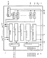
図1は本発明の実施の形態1のTFTソースドライバLSIチップの構成図であって、384本のアナログ電圧出力チャンネルを有するTFTソースドライバである。なお、図1において、図6と同じものには同じ符号を付してある。
【0019】
図1の実施の形態1のLSIチップ1は、コントローラ101と、抵抗ストリング102と、2nビット双方向シフトレジスタ103と、データレジスタ104と、レベルシフタ105と、マルチプレクサ106と、出力回路107と、384ビットシフトレジスタ11と、スイッチS001,S002,…,S384とを備えている。
【0020】
また、図1の実施の形態1のLSIチップ1は、電源VDD,VCCの入力端子と、基準電源VSSの入力端子と、それぞれ2n(=m)本の電圧VH(2n:0),VL(2n:0)の入力端子と、それぞれnビットの階調データDA(n:0),DB(n:0),DC(n:0),DD(n:0),DE(n:0),DF(n:0)の入力端子と、クロックパルスCPの入力端子と、出力極性信号POLの入力端子と、ロードパルスLOADの入力端子と、ダウンシフト信号EDの入力端子と、アップシフト信号EUの入力端子と、384本のアナログ電圧出力O001,O002,…,O384の出力端子と、テストイネーブル信号TEST ENの入力端子と、テスト出力TEST OUTの出力端子とを備えている。
【0021】
この実施の形態1のLSIチップ1は、従来のLSIチップ100(図6参照)において、テスト回路を設けたものである。実施の形態1のテスト回路は、アナログ電圧出力本数に相当するビット数の384ビットシフトレジスタ11と、上記アナログ電圧出力本数に相当する数のスイッチS001−S384と、テストイネーブル信号TEST ENの入力端子と、テスト出力TEST OUTの出力端子とによって構成されている。
【0022】
コントローラ101は、1出力当たりnビットの計6出力分の階調データDA(n:0),DB(n:0),DC(n:0),DD(n:0),DE(n:0),DF(n:0)に応じて、それぞれの出力ごとに2nビットのアナログ階調データを生成して双方向シフトレジスタ103に出力し、双方向シフトレジスタ103およびデータレジスタ104ならびにマルチプレクサ106の動作を制御するとともに、入力された出力極性信号POLに応じて出力回路107の出力反転機能を制御する。
【0023】
抵抗ストリング102は、抵抗分圧によって、上記nビットの階調データに応じたアナログ階調電圧を生成し、マルチプレクサ106に出力する。
【0024】
双方向シフトレジスタ103は、コントローラ101から入力された上記2nビットのアナログ階調データを、6出力分ずつクロックパルスCPに同期して取り込む。この双方向シフトレジスタ103は、ダウンシフト信号EDおよびアップシフト信号EUに従って、アップまたはダウンの双方向のシフト動作を切替可能である。
【0025】
データレジスタ104は、双方向シフトレジスタ103に取り込まれた上記アナログ階調データを、ロードパルスLOADに同期してラッチし、レベルシフタ105に出力する。
【0026】
レベルシフタ105は、入力信号の電圧振幅を変換するものであって、例えば、3[V]振幅の信号を10[V]振幅の信号に電圧変換する。
【0027】
マルチプレクサ106は、データレジスタ104でラッチされた1出力当たり2nビットのアナログ階調データのそれぞれに相当するアナログ階調電圧を、抵抗ストリングス102で生成されたアナログ階調電圧から選択し、出力回路107に出力する。
【0028】
出力回路107は、マルチプレクサ106で選択されたアナログ階調電圧を、電流駆動能力を増幅してアナログ電圧出力O001−O384として出力する。
【0029】
実施の形態1のテスト回路において、384ビットシフトレジスタ11は、テストイネーブル信号TEST ENが入力されているテストモードのとき(例えばTEST ENがHレベルのとき)に、イネーブルとなり、クロックパルスCPに同期してデータを1ビットずつシフトし、384ビットの内のいずれか1ビットを順次”1”(例えばHレベル)にする。また、384ビットシフトレジスタ11は、TEST ENが入力されていないオペレーションモードのとき(例えばTEST ENがLレベルのとき)には、ディスエーブルになり、384ビットを全て”0”(例えばLレベル)にする。
【0030】
スイッチS(n)(n=001,002,…,384)は、384ビットシフトレジスタ11の第nビットの出力によって個別にON/OFF制御され、上記の第nビットの出力が”1”のときにONして導通端子間を導通し、上記第nビットの出力が”0”のときにOFFして導通端子間を非導通にする。スイッチS(n)の制御端子は、384ビットシフトレジスタ11の第nビットの出力に接続されており、スイッチS(n)の一方の導通端子は、アナログ電圧出力O(n)に接続されている。スイッチS000−S384の他方の導通端子は、全てテスト出力TEST OUTに共通接続されている。
【0031】
図2は実施の形態1のLSIチップ1を実装したチップキャリアの上面図である。なお、図2において、図7と同じものには同じ符号を付してある。図2の実施の形態1のチップキャリア20は、ユーザエリア201内にLSIチップ1が実装されており、このユーザエリア201で個片に切り抜かれて、TFTソースドライバデバイスのキャリアパッケージになる。
【0032】
図2の実施の形態1のチップキャリア20には、LSIチップ1のそれぞれの入力端子に個別に接続する複数の入力リード202と、LSIチップ100のアナログ出力電圧O001−O384の出力端子のそれぞれに個別に接続する多数の出力リード203と、出力リード203のそれぞれに個別に接続する多数のテストパッド204と、LSIチップ1のテストイネーブル信号TEST ENの入力端子に接続するテスト入力パッド(テスト入力リード)21と、LSIチップ1のテスト出力TEST OUTの出力端子に接続するテスト出力パッド(テスト出力リード)22とが設けられている。
【0033】
この実施の形態1のチップキャリア20は、上記従来のチップキャリア200(図7参照)において、ユーザエリア201内に、テスト入力パッド21およびテスト出力パッド22を設けたものである。
【0034】
従って、この実施の形態1のチップキャリア20では、ユーザエリア201は、テスト入力パッド21、テスト出力パッド22、複数の入力リード202、および複数の出力リードが設けられており、LSIチップ1が実装され、個片に切り抜かれてTFTソースドライバデバイスのキャリアパケージとなるエリアであって、出力リード203の端部にそれぞれ設けられたテストパッド204を含まないエリアである。
【0035】
テスト入力パッド21およびテスト出力パッド22は、複数の入力リード202の配列側に設けられている。入力リード202の本数は出力リード203のそれよりも少なく、入力リード202の幅(ピッチ)は出力リード203のそれよりも広くすることができる。従って、テスト出力パッド22を、複数の出力リード203の配列側ではなく、出力リード203とは反対側の入力リード202側に配置することによって、幅が広いテスト出力パッド22を設けることできるので、テスト出力パッド22の探針が容易になる。
【0036】
実施の形態1のテスト回路のテストモードにおいての動作を以下に説明する。テストモード(例えばテストイネーブル信号TEST ENがHレベル)では、384ビットシフトレジスタ11は、イネーブルになり、クロックパルスCPが最初に入力されると、第001ビットの出力のみが”1”(例えばHレベル)になり、スイッチS001のみをONにする。
【0037】
384ビットシフトレジスタ11は、384ビットの出力の内の1ビットのみを”1”とし、その他のビットを”0”(例えばLレベル)にするので、スイッチS001がONのときには、他のスイッチS002−S384はOFFである。
【0038】
これによって、出力回路107のアナログ電圧出力O001−O384の内、出力O001のみが、スイッチS001を介してテスト出力TEST OUTに出力され、従ってキャリアパッケージ上のテスト出力パッド22に出力される。
【0039】
次に、384ビットシフトレジスタ11は、2つ目のクロックパルスCPが入力されると、データをシフトさせ、第001ビットの出力はLレベルになって、第002ビットの出力のみがHレベルになり、スイッチS001をOFFして、スイッチS002のみをONする。スイッチS003−S384は、OFFのままである。
【0040】
これによって、アナログ電圧出力O002のみが、スイッチS002を介してテスト出力TEST OUTに出力され、従ってキャリアパッケージ上のテスト出力パッド22に出力される。
【0041】
以下同様に、クロックパルスCPの入力ごとに384ビットシフトレジスタ11の上位ビットが順次Hレベルとなり、そのHレベルの1つのビットに応じて、1つのスイッチSのみが順次ONになり、1本のアナログ電圧出力Oのみがキャリアパッケージ上のテスト出力パッド22に順次出力される。
【0042】
このテストモードでは、LSIチップ1に設けたテスト回路によってテスト出力パッド22に全てのアナログ電圧出力を順次出力することができるので、TFTソースドライバデバイスのキャリアパッケージ上において、探針が困難な狭ピッチの出力リード203に探針することなく、探針が容易なリードである入力リード202およびテスト入力パッド21ならびにテスト出力パッド22に探針すれば、全てのアナログ電圧出力を順次測定することができる。
【0043】
以上のように実施の形態1によれば、狭ピッチのため探針が困難である出力リードを探針することなく、個片のキャリアパッケージに実装されたTFTソースドライバLSIチップの全てのアナログ電圧出力を容易に測定できる。
【0044】
実施の形態2
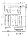
図3は本発明の実施の形態2のTFTソースドライバLSIチップの構成図であって、384本のアナログ電圧出力チャンネルを有するTFTソースドライバである。なお、図3において、図1と同じものあるいはそれに相当するものには同じ符号を付してある。
【0045】
図3の実施の形態2のLSIチップ2は、コントローラ101と、抵抗ストリング102と、2nビット双方向シフトレジスタ103と、データレジスタ104と、レベルシフタ105と、マルチプレクサ106と、出力回路107と、192ビットシフトレジスタ12と、スイッチS001,S002,…,S384とを備えている。
【0046】
また、図3の実施の形態2のLSIチップ2は、電源VDD,VCCの入力端子と、基準電源VSSの入力端子と、それぞれ2n(=m)本の電圧VH(2n:0),VL(2n:0)の入力端子と、それぞれnビットの階調データDA(n:0),DB(n:0),DC(n:0),DD(n:0),DE(n:0),DF(n:0)と、クロックパルスCPの入力端子と、出力極性信号POLの入力端子と、ロードパルスLOADの入力端子と、ダウンシフト信号EDの入力端子と、アップシフト信号EUの入力端子と、384本のアナログ電圧出力O001,O002,…,O384の出力端子と、テストイネーブル信号TEST ENの入力端子と、テスト出力ODD TEST OUTの出力端子と、テスト出力EVEN TEST OUTの出力端子とを備えている。
【0047】
この実施の形態2のLSIチップ2は、上記実施の形態1のLSIチップ10(図1参照)において、テスト回路の構成を簡略にしたものである。実施の形態2のテスト回路は、アナログ電圧出力本数の半分に相当するビット数の192ビットシフトレジスタ12と、アナログ電圧出力本数に相当する数のスイッチS001−S384と、テストイネーブル信号TEST ENの入力端子と、2本のテスト出力ODD TEST OUT,EVEN TEST OUTの出力端子とによって構成されている。
【0048】
実施の形態2のテスト回路において、192ビットシフトレジスタ12は、テストイネーブル信号TEST ENが入力されているテストモードのとき(例えばTEST ENがHレベルのとき)に、イネーブルとなり、クロックパルスCPに同期してデータを1ビットずつシフトし、192ビットの内のいずれか1ビットを順次”1”(例えばHレベル)にする。また、192ビットシフトレジスタ12は、TEST ENが入力されていないオペレーションモードのとき(例えばTEST ENがLレベルのとき)には、ディスエーブルになり、192ビットを全て”0”(例えばLレベル)にする。
【0049】
スイッチS(2n−1)(n=001,002,…,192)およびS(2n)は、192ビットシフトレジスタ12の第nビットの出力が”1”のときにONして導通端子間を導通し、上記第nビットの出力が”0”のときにOFFして導通端子間を非導通にする。スイッチS(2n−1)およびS(2n)の制御端子は、192ビットシフトレジスタ12の第nビットの出力に接続されている。スイッチS(2n−1)の一方の導通端子は、アナログ電圧出力O(2nー1)に接続されており、スイッチS(2n)の一方の導通端子は、アナログ電圧出力O(2n)に接続されている。奇数番目のスイッチS001,S003,…,S383の他方の端子は、テスト出力ODD TEST OUTに共通接続されており、偶数番目のスイッチS002,S004,…,S384の他方の端子は、テスト出力EVEN TEST OUTに共通接続されている。
【0050】
実施の形態2のLSIチップ2を実装したチップキャリアは、上記実施の形態1のチップキャリア20(図2参照)において、ユーザエリア201内のテスト出力パッド22を2本にして、テスト出力ODD TEST OUTに接続するテスト出力パッド22(22−ODDとする)と、テスト出力EVEN TEST OUTの出力端子に接続するテスト出力パッド22(22−EVENとする)を設けたものである。
【0051】
従って、この実施の形態2のチップキャリアでは、上記実施の形態1と同様に、ユーザエリア201は、テスト入力パッド21、テスト出力パッド22−ODD,22−EVEN、複数の入力リード202、および複数の出力リードが設けられており、LSIチップ1が実装され、個片に切り抜かれてTFTソースドライバデバイスのキャリアパケージとなるエリアであって、出力リード203の端部にそれぞれ設けられたテストパッド204を含まないエリアである。
【0052】
また、上記実施の形態1と同様に、テスト入力パッド21ならびにテスト出力パッド22−ODDおよび22−EVENは、複数の入力リード202の配列側に設けられている。このようにテスト出力パッド22−ODDおよび22−EVENを入力リード202側に配置することによって、上記実施の形態1と同様に、幅が広いテスト出力パッド22−ODDおよび22−EVENを設けることできるので、テスト出力パッド22−ODDおよび22−EVENの探針が容易になる。
【0053】
実施の形態2のテスト回路のテストモードにおいての動作を以下に説明する。テストモード(例えばテストイネーブル信号TEST ENがHレベル)では、192ビットシフトレジスタ12は、イネーブルになり、クロックパルスCPが最初に入力されると、第001ビットの出力のみが”1”(例えばHレベル)になり、スイッチS001およびS002のみをONにする。
【0054】
192ビットシフトレジスタ12は、192ビットの出力の内の1ビットのみを”1”とし、その他のビットを”0”(例えばLレベル)にするので、スイッチS001およびS002がONのときには、他のスイッチS003−S384はOFFである。
【0055】
これによって、出力回路107のアナログ電圧出力O001−O384の内、出力O001は、スイッチS001を介してテスト出力ODD TEST OUTに出力され、従ってキャリアパッケージ上のテスト出力パッド22−ODDに出力される。また、アナログ電圧出力O002は、スイッチS002を介してテスト出力EVEN TEST OUTに出力され、従ってキャリアパッケージ上のテスト出力パッド22−EVENに出力される。
【0056】
次に、192ビットシフトレジスタ12は、2つ目のクロックパルスCPが入力されると、データをシフトさせ、第001ビットの出力はLレベルになって、第002ビットの出力のみがHレベルになり、スイッチS001およびS002をOFFして、スイッチS003およびS004をONする。スイッチS005−S384は、OFFのままである。
【0057】
これによって、アナログ電圧出力O003が、スイッチS003を介してテスト出力ODD TEST OUTに出力され、従ってキャリアパッケージ上のテスト出力パッド22−ODDに出力される。また、アナログ電圧出力O004が、スイッチS004を介してテスト出力EVEN TEST OUTに出力され、従ってキャリアパッケージ上のテスト出力パッド22−EVENに出力される。
【0058】
以下同様に、クロックパルスCPの入力ごとに192ビットシフトレジスタ12の上位ビットが順次Hレベルとなり、そのHレベルの1つのビットに応じて、2つのスイッチSのみが順次ONになり、2本のアナログ電圧出力Oがキャリアパッケージ上のテスト出力パッド22−ODDおよび22−EVENにそれぞれ順次出力される。
【0059】
このテストモードでは、LSIチップ2に設けたテスト回路によって2本のテスト出力パッド22(22−ODDおよび22−EVEN)に全てのアナログ電圧出力を順次出力することができるので、TFTソースドライバデバイスのキャリアパッケージ上において、探針が困難な狭ピッチの出力リード203に探針することなく、探針が容易なリードである入力リード202およびテスト入力パッド21ならびに2本のテスト出力パッド22に探針すれば、全てのアナログ電圧出力を順次測定することができる。
【0060】
以上のように実施の形態2によれば、テスト回路のシフトレジスタのビット数を上記実施の形態1の半分にした構成で、上記実施の形態1と同様の効果が得られる。さらに、テスト出力の本数を3本,4本,…に増やすことが可能であれば、シフトレジスタのビット数を上記実施の形態1の1/3,1/4,…にすることも可能である。
【0061】
実施の形態3
図4は本発明の実施の形態3のTFTソースドライバのLSIチップの構成図であって、384本のアナログ電圧出力チャンネルを有するTFTソースドライバである。なお、図4において、図3と同じものには同じ符号を付してある。
【0062】
図4の実施の形態3のLSIチップ3は、コントローラ101と、抵抗ストリング102と、2nビット双方向シフトレジスタ103と、データレジスタ104と、レベルシフタ105と、マルチプレクサ106と、出力回路107と、192ビットシフトレジスタ21と、スイッチS001,S002,…,S192とを備えている。
【0063】
また、図4の実施の形態3のLSIチップ3は、電源VDD,VCCの入力端子と、基準電源VSSの入力端子と、それぞれ2n(=m)本の電圧VH(2n:0),VL(2n:0)の入力端子と、それぞれnビットの階調データDA(n:0),DB(n:0),DC(n:0),DD(n:0),DE(n:0),DF(n:0)の入力端子と、クロックパルスCPの入力端子と、出力極性信号POLの入力端子と、ロードパルスLOADの入力端子と、ダウンシフト信号EDの入力端子と、アップシフト信号EUの入力端子と、384本のアナログ電圧出力O001,O002,…,O384の出力端子と、テストイネーブル信号TEST ENの入力端子と、テスト出力TEST OUTの出力端子とを備えている。
【0064】
この実施の形態3のLSIチップ30は、上記実施の形態2のLSIチップ20(図3参照)において、テスト回路の構成をさらに簡略にしたものである。実施の形態3のテスト回路は、アナログ電圧出力本数の半分に相当するビット数の192ビットシフトレジスタ12と、上記アナログ電圧出力本数の半分に相当する数のスイッチS001−S192と、テストイネーブル信号のTEST ENの入力端子と、テスト出力TEST OUTの出力端子とによって構成されている。
【0065】
実施の形態3のテスト回路において、スイッチS(n)(n=001,002,…,192)は、192ビットシフトレジスタ12の第nビットの出力によって個別にON/OFF制御され、上記の第nビットの出力が”1”のときにONして導通端子間を導通し、上記第nビットの出力が”0”のときにOFFして導通端子間を非導通にする。スイッチS(n)の制御端子は、192ビットシフトレジスタ12の第nビットの出力に接続されており、スイッチS(n)の一方の導通端子は、アナログ電圧出力O(2n−1)に接続されている。スイッチS000−S192の他方の導通端子は、全てテスト出力TEST OUTに共通接続されている。
【0066】
実施の形態3のLSIチップ3を実装したチップキャリアは、上記実施の形態1のチップキャリア20(図2参照)と同様である。
【0067】
従って、この実施の形態3のチップキャリアでは、上記実施の形態1と同様に、ユーザエリア201は、テスト入力パッド21、テスト出力パッド22、複数の入力リード202、および複数の出力リードが設けられており、LSIチップ1が実装され、個片に切り抜かれてTFTソースドライバデバイスのキャリアパケージとなるエリアであって、出力リード203の端部にそれぞれ設けられたテストパッド204を含まないエリアである。
【0068】
また、上記実施の形態1と同様に、テスト入力パッド21およびテスト出力パッド22は、複数の入力リード202の配列側に設けられている。このようにテスト出力パッド22を入力リード202側に配置することによって、幅が広いテスト出力パッド22を設けることできるので、テスト出力パッド22の探針が容易になる。
【0069】
TFTソースドライバの出力回路107は、出力極性信号POLに従って、奇数番目の出力O(2n−1)と、偶数番目の出力O(2n)とを入れ替えることができるようになっている。
【0070】
図5は出力回路107の構成図である。図5において、出力回路107は、出力アンプPAおよびNAと、セレクタPSおよびNSとを備えている。
【0071】
出力アンプPAは、マルチプレクサ106のデコード出力Pをセンスおよび増幅してセレクタPSに出力し、出力アンプNAは、マルチプレクサ106のデコード出力Nをセンスおよび増幅してセレクタNSに出力する。
【0072】
セレクタPSは、デコード出力Pを出力極性信号POLに従って奇数番目の出力O(2n−1)または偶数番目の出力O(2n)に出力し、セレクタNSは、デコード出力Nを出力極性信号POLに従って偶数番目の出力端子O(2n)または奇数番目の出力O(2n−1)に出力する。
【0073】
出力極性信号POLが”0”(例えばLレベル)のときには、デコード出力Pは出力O(2n−1)に、デコード出力Nは出力O(2n)にそれぞれ出力され、出力極性信号POLが”1”(例えばHレベル)のときには、出力が反転して、デコード出力Pは出力O(2n)に、デコード出力Nは出力O(2n−1)にそれぞれ出力される。
【0074】
このように、出力回路107は、出力極性信号POLに応じて、奇数番目の出力O(2n−1)と偶数番目の出力O(2n)とを入れ替えることができるので、VH側の出力およびVL側の出力のいずれをも選択して奇数番目の出力O(2n−1)に出力することができる。
【0075】
この出力回路107の出力反転機能を用いて、出力極性信号POLのHレベルおよびLレベルのそれぞれについて、奇数番目の出力O(2n−1)をキャリアパッケージ上のテスト出力パッド22で測定すれば、384本の全てのアナログ電圧出力特性を測定できる。
【0076】
実施の形態3のテスト回路のテストモードにおいての動作を以下に説明する。まず、出力極性信号POLを”0”(例えばLレベル)に固定してテストモードにする。これによって、アナログ電圧出力O(2n−1)はデコード出力Pとなる。
【0077】
テストモード(例えばテストイネーブル信号TEST ENがHレベル)では、192ビットシフトレジスタ12は、イネーブルになり、クロックパルスCPが最初に入力されると、第001ビットの出力のみが”1”(例えばHレベル)になり、スイッチS001のみをONにする。
【0078】
192ビットシフトレジスタ12は、192ビットの出力の内の1ビットのみを”1”とし、その他のビットを”0”(例えばLレベル)にするので、スイッチS001がONのときには、他のスイッチS002−S192はOFFである。
【0079】
これによって、出力回路107のアナログ電圧出力O001−O384の内、出力O001(デコード出力P)のみが、スイッチS001を介してテスト出力TEST OUTに出力され、従ってキャリアパッケージ上のテスト出力パッド22に出力される。
【0080】
次に、192ビットシフトレジスタ12は、2つ目のクロックパルスCPが入力されると、データをシフトさせ、第001ビットの出力はLレベルになって、第002ビットの出力のみがHレベルになり、スイッチS001をOFFして、スイッチS002のみをONする。スイッチS003−S192は、OFFのままである。
【0081】
これによって、アナログ電圧出力O003(デコード出力P)のみが、スイッチS002を介してテスト出力TEST OUTに出力され、従ってキャリアパッケージ上のテスト出力パッド22に出力される。
【0082】
以下同様に、クロックパルスCPの入力ごとに192ビットシフトレジスタ11の上位ビットが順次Hレベルとなり、そのHレベルの1つのビットに応じて、1つのスイッチSのみが順次ONになり、1本のアナログ電圧出力O(デコード出力P)のみがキャリアパッケージ上のテスト出力パッド22に順次出力される。
【0083】
192ビットシフトレジスタ12の第192ビットがHレベルとなり、アナログ電圧出力O383(デコード出力P)がキャリアパッケージ上のテスト出力パッド22に出力されたら、出力極性信号POLを”1”(例えばHレベル)に反転させる。これによって、アナログ電圧出力O(2n−1)は、デコード出力Pからデコード出力Nに反転する。つまり、アナログ電圧出力O(2n−1)は、出力極性信号POLがLレベルだったときのアナログ電圧出力O(2n)となり、アナログ電圧出力O(2n)は、出力極性信号POLがLレベルだったときのアナログ電圧出力O(2n−1)となる。
【0084】
この出力極性信号POLがHレベルに反転したテストモードでは、クロックパルスCPの入力ごとに192ビットシフトレジスタ11の上位ビットが順次Hレベルとなり、そのHレベルの1つのビットに応じて、1つのスイッチSのみが順次ONになり、1本のアナログ電圧出力O(デコード出力N)のみがキャリアパッケージ上のテスト出力パッド22に順次出力される。
【0085】
この出力極性信号POLをLレベルおよびHレベルとしたテストモードでは、LSIチップ3に設けたテスト回路によってテスト出力パッド22に全てのアナログ電圧出力を順次出力することができるので、TFTソースドライバデバイスのキャリアパッケージ上において、探針が困難な狭ピッチの出力リード203に探針することなく、探針が容易なリードである入力リード202およびテスト入力パッド21ならびにテスト出力パッド22に探針すれば、全てのアナログ電圧出力を順次測定することができる。
【0086】
なお、この実施の形態3では、奇数番目のアナログ電圧出力OをスイッチSに接続した構成を説明したが、偶数番目のアナログ電圧出力OをスイッチSに接続した構成も可能である。
【0087】
以上のように実施の形態3によれば、テスト回路のシフトレジスタのビット数およびスイッチSの数を上記実施の形態1の半分にした構成で、上記実施の形態1と同様の効果が得られる。
【0088】
なお、上記実施の形態1ー3のテスト回路のシフトレジスタは、テストイネーブル信号TEST ENによってイネーブルとなり、TFTソースドライバのクロックパルスCPに同期してデータをシフトさせる構成であるが、リセットまたはセット付きのシフトレジスタを設け、テストイネーブル信号TEST ENの入力端子からシフトレジスタの動作クロックを入力する構成も可能である。この構成では、オペレーションモードにするときにはクロックを入力せず、テストモードにするときにはクロックを入力する。オペレーションモードでは、全てのビット出力がリセットまたはセットされている。また、テストモードでは、クロックを入力するごとに、ただ1つのHレベルのビットが第001ビットから順次上位ビットにシフトし、上記実施の形態1−3と同様の動作ができる。また、シフトレジスタの先頭または最終ビットにダミービットを設け、オペレーションモードでは、ただ1つのHレベルのビットをダミービットに保持しておき、テストモードにおいてのクロック入力ごとに、上記ただ1つのHレベルのビットが上記ダミービットから順次シフトする構成も可能である。
【0089】
また、TFTソースドライバのアナログ電圧出力部(HV部)は、一般に10[V]ほどの高電圧を出力するように構成されており、入力部(LV部)は、3−5[V]の入力電圧で動作するように構成されている。HV部とLV部の回路構成の場合、テスト回路のシフトレジスタおよびスイッチは、HV部で構成すればよい。しかしながら、HV部は面積の大きな回路になってしまうので、上記シフトレジスタをLV部で構成し、上記スイッチをHV部で構成するほうが経済的である。この場合には、シフトレジスタのビット出力であるLV部の電圧レベルをスイッチのON/OFF制御のHV部の電圧レベルに変換することが必要であるため、それぞれのノードに電圧レベル変換回路(電圧レベルシフト回路)を挿入する。
【0090】
また、テスト入力リード(テスト入力パッド)21およびテスト出力リード(テスト出力パッド)22は、針当てをしやすい任意の形態で、ユーザエリア内に設けることが可能である。
【0091】
【発明の効果】
以上説明したように本発明によれば、個片のキャリアパッケージに実装されたアナログ電圧出力ドライバLSIチップの電気特性を容易に確認できるという効果がある。
【図面の簡単な説明】
【図1】 本発明の実施の形態1のTFTソースドライバLSIチップの構成図である。
【図2】 図1のLSIチップを実装したチップキャリアの上面構成図である。
【図3】 本発明の実施の形態2のTFTソースドライバLSIチップの構成図である。
【図4】 本発明の実施の形態3のTFTソースドライバLSIチップの構成図である。
【図5】 TFTソースドライバLSIチップにおいての出力回路の構成図である。
【図6】 従来のTFTソースドライバLSIチップの構成図である。
【図7】 図6のLSIチップを実装したチップキャリアの上面構成図である。
【符号の説明】
1,2,3 TFTソースドライバLSIチップ、 11,12 シフトレジスタ、 S001,S002,…,S384 スイッチ、 20 チップキャリア、 21 テスト入力リード(テスト入力パッド)、 22 テスト出力リード(テスト出力パッド)。[0001]
BACKGROUND OF THE INVENTION
The present invention is an analog voltage output driver LSI chip having a number of output channels, such as a TFT source driver LSI chip, which is provided with a test circuit for evaluation and analysis.ToIt is related.
[0002]
[Prior art]
As a typical analog voltage output driver having a large number of output channels, a TFT source driver used in a liquid crystal panel or the like is a multi-output channel analog voltage having hundreds of analog voltage output terminals for gradation display. Output driver.
[0003]
FIG. 6 is a block diagram of a conventional TFT source driver LSI chip, which is a TFT source driver LSI chip having 384 analog voltage output channels.
[0004]
The conventional LSI chip 100 of FIG. 6 includes a controller 101, a
[0005]
Further, the conventional LSI chip 100 of FIG. 6 includes 2n (= m) voltages VH (2n: 0) and VL (2n: 0), respectively, of the input terminals of the power supplies VDD and VCC and the input terminal of the reference power supply VSS. ) And input terminals DA (2: 0), DB (2: 0), DC (2: 0), DD (2 :) for n-bit data A, B, C, D, E, and F, respectively. 0), DE (2: 0), DF (2: 0), clock pulse CP input terminal, output polarity signal POL input terminal, load pulse LOAD input terminal, and downshift signal ED input terminal , And an output terminal of 384 analog voltage outputs O001, O002,..., O384.
[0006]
The TFT source driver LSI chip is mounted in a user area of a chip carrier such as a carrier tape or film, and the chip carrier on which the TFT source driver LSI chip is mounted is a tape carrier package (TCP) or a chip-on-film. The carrier package such as (COF) is cut into individual pieces in the user area. The TCP mounting and the COF mounting have the same basic configuration, although there are differences in the material of the chip carrier.
[0007]
In this way, a TFT source driver device in which a TFT source driver LSI chip is mounted on a carrier package (such as TCP mounting or chip COF mounting) is manufactured. The TFT source driver device is incorporated into a TFT liquid crystal panel or a printed circuit board.
[0008]
FIG. 7 is a top view of a chip carrier on which a conventional LSI chip 100 is mounted. The conventional chip carrier 200 of FIG. 7 has an LSI chip 100 mounted in a user area 201, and is cut into individual pieces in the user area 201 to form a carrier package for a TFT source driver device.
[0009]
The conventional chip carrier 200 of FIG. 7 is individually connected to a plurality of input leads 202 individually connected to the respective input terminals of the LSI chip 100 and to output terminals of the analog voltage outputs O001 to O384 of the LSI chip 100. A number of output leads 203 and a number of test pads 204 individually connected to the output leads 203 are provided.
[0010]
The test pad 204 is provided outside the user area 201, and is provided to apply test needles in sorting and shipping inspection by measuring the electrical characteristics of the LSI chip 100 mounted on the chip carrier 200. Pad. By providing the test pad 204 outside the user area 201, there is an advantage that needle marks do not remain in the user area 201 (individual carrier package).
[0011]
Further, in a TFT source driver having hundreds of multi-output channels, the pattern pitch of the output leads 203 becomes narrow, making it difficult to arrange a large number of test pads 204. For this reason, it is also possible to improve the ease of contact of the test needles by devising an arrangement in which the test pads 204 are stacked in several stages. Alternatively, as described in, for example, Japanese Patent Laid-Open No. 2000-131393, the number of test pads 204 can be reduced by commonly connecting a large number of output leads 204 outside the user area 201.
[0012]
[Problems to be solved by the invention]
However, since the test pad does not remain in the individual carrier package in the above-described conventional technology, when it is necessary to evaluate and analyze the LSI chip at the time of return of the device, etc., all the narrow-pitch output leads are searched. Need to measure the analog output voltage of hundreds of output channels. The pitch of the output leads is, for example, 80 [μm], and all of these narrow pitch output leads must be probed with a high precision manipulator. Moreover, in order to confirm the output of 384 lines, the needle pad of the manipulator was required 384 times.
[0013]
As described above, in the conventional technology, it is difficult to apply the needle after the device is formed. Therefore, when the device is returned, the electrical characteristics of the analog voltage output driver LSI chip for evaluation and analysis can be confirmed. There was a problem that it was difficult.
[0014]
The present invention has been made to solve such a conventional problem, and an object of the present invention is to make it possible to easily confirm the electrical characteristics of an analog voltage output driver LSI chip mounted on a piece of carrier package. It is what.
[0015]
[Means for Solving the Problems]
The analog voltage output driver LSI chip of the present invention is
In an analog voltage output driver LSI having a large number of analog voltage output channels,
Number of analog voltage outputs aboveHalf ofBit register test shift register circuit;
Number of analog voltage outputs aboveHalf ofA number of test switch circuits;
A test output terminal to which the test switch circuit is connected in common;
With
The test switch circuit is individually ON / OFF controlled by the bit output of the test shift register circuit,
Each of the test switch circuits is individually connected to one of the two analog voltage outputs that can be inverted from each other,
Any one of the test switch circuits is turned ON, and one analog voltage output connected to the test switch circuit is output to the test output terminal.
It is characterized by this.
[0016]
Also,Another analog voltage output driver LSI chip of the present invention is:
In an analog voltage output driver LSI having a large number of analog voltage output channels,
A test shift register circuit having a number of bits corresponding to the number of analog voltage outputs;
A number of test switch circuits corresponding to the number of the analog voltage outputs;
A test output terminal to which the test switch circuit is connected in common;
With
The test switch circuit is individually ON / OFF controlled by the bit output of the test shift register circuit,
One of the test switch circuits is turned ON, and one analog voltage output connected to the test switch circuit is output to the test output terminal,
The test shift register circuit is provided with a dummy bit for holding data for turning on any one of the test switch circuits.
It is characterized by this.
[0018]
DETAILED DESCRIPTION OF THE INVENTION
FIG. 1 is a configuration diagram of a TFT source driver LSI chip according to the first embodiment of the present invention, which is a TFT source driver having 384 analog voltage output channels. In FIG. 1, the same components as those in FIG. 6 are denoted by the same reference numerals.
[0019]
1 includes a controller 101, a
[0020]
In addition, the
[0021]
The
[0022]
The controller 101 has gradation data DA (n: 0), DB (n: 0), DC (n: 0), DD (n: 0), DE (n: 0n), DF (n: 0), 2n-bit analog gradation data is generated for each output and output to the
[0023]
The
[0024]
The
[0025]
The data register 104 latches the analog gradation data fetched into the
[0026]
The
[0027]
The
[0028]
The
[0029]
In the test circuit of the first embodiment, the 384-bit shift register 11 is enabled in the test mode in which the test enable signal TEST EN is input (for example, when TEST EN is at the H level), and is synchronized with the clock pulse CP. Then, the data is shifted bit by bit, and any one of the 384 bits is sequentially set to “1” (for example, H level). Further, the 384-bit shift register 11 is disabled in an operation mode in which TEST EN is not input (for example, when TEST EN is at L level), and all 384 bits are set to “0” (for example, L level). To.
[0030]
The switches S (n) (n = 001, 002,..., 384) are individually ON / OFF controlled by the nth bit output of the 384 bit shift register 11, and the nth bit output is “1”. It is sometimes turned on to conduct between the conducting terminals, and when the output of the nth bit is "0", it is turned off to render the conducting terminals non-conducting. The control terminal of the switch S (n) is connected to the n-th bit output of the 384-bit shift register 11, and one conduction terminal of the switch S (n) is connected to the analog voltage output O (n). Yes. The other conduction terminals of the switches S000-S384 are all commonly connected to the test output TEST OUT.
[0031]
FIG. 2 is a top view of a chip carrier on which the
[0032]
2 includes a plurality of input leads 202 individually connected to respective input terminals of the
[0033]
In the chip carrier 20 of the first embodiment, a test input pad 21 and a
[0034]
Therefore, in the chip carrier 20 of the first embodiment, the user area 201 is provided with the test input pad 21, the
[0035]
The test input pad 21 and the
[0036]
The operation of the test circuit of the first embodiment in the test mode will be described below. In the test mode (for example, the test enable signal TEST EN is at the H level), the 384-bit shift register 11 is enabled, and when the clock pulse CP is first input, only the output of the 001-th bit is “1” (for example, H Level) and only the switch S001 is turned ON.
[0037]
The 384-bit shift register 11 sets only one bit of the 384-bit output to “1” and sets the other bits to “0” (for example, L level). Therefore, when the switch S001 is ON, the other switch S002 -S384 is OFF.
[0038]
As a result, only the output O001 of the analog voltage outputs O001 to O384 of the
[0039]
Next, when the second clock pulse CP is input, the 384-bit shift register 11 shifts the data, the output of the 001th bit becomes L level, and only the output of the 002st bit becomes H level. Thus, the switch S001 is turned off and only the switch S002 is turned on. Switches S003-S384 remain OFF.
[0040]
As a result, only the analog voltage output O002 is output to the test output TEST OUT via the switch S002, and thus to the
[0041]
Similarly, for each input of the clock pulse CP, the upper bits of the 384-bit shift register 11 are sequentially set to the H level, and only one switch S is sequentially turned ON in response to one bit of the H level. Only the analog voltage output O is sequentially output to the
[0042]
In this test mode, all analog voltage outputs can be sequentially output to the
[0043]
As described above, according to the first embodiment, all analog voltages of the TFT source driver LSI chip mounted on the individual carrier package can be obtained without probing the output leads that are difficult to probe due to the narrow pitch. The output can be easily measured.
[0044]
FIG. 3 is a configuration diagram of the TFT source driver LSI chip according to the second embodiment of the present invention, which is a TFT source driver having 384 analog voltage output channels. In FIG. 3, the same reference numerals are assigned to the same components as those in FIG.
[0045]
The
[0046]
Further, the
[0047]
The
[0048]
In the test circuit according to the second embodiment, the 192-bit shift register 12 is enabled in the test mode in which the test enable signal TEST EN is input (for example, when TEST EN is at the H level), and is synchronized with the clock pulse CP. Then, the data is shifted bit by bit, and any one of the 192 bits is sequentially set to “1” (for example, H level). Further, the 192-bit shift register 12 is disabled in an operation mode in which TEST EN is not input (for example, when TEST EN is at L level), and all 192 bits are set to “0” (for example, L level). To.
[0049]
The switches S (2n−1) (n = 001, 002,..., 192) and S (2n) are turned on when the output of the nth bit of the 192-bit shift register 12 is “1”, and between the conduction terminals. When the output of the nth bit is “0”, it is turned off to make the conduction terminals non-conductive. The control terminals of the switches S (2n−1) and S (2n) are connected to the n-th bit output of the 192-bit shift register 12. One conduction terminal of the switch S (2n-1) is connected to the analog voltage output O (2n-1), and one conduction terminal of the switch S (2n) is connected to the analog voltage output O (2n). Has been. The other terminals of the odd-numbered switches S001, S003,..., S383 are commonly connected to the test output ODD TEST OUT, and the other terminals of the even-numbered switches S002, S004,. Commonly connected to OUT.
[0050]
The chip carrier on which the
[0051]
Therefore, in the chip carrier of the second embodiment, as in the first embodiment, the user area 201 includes the test input pad 21, the test output pads 22-ODD and 22-EVEN, the plurality of input leads 202, and the plurality of input leads 202. Output leads, test chip 204 provided on the end of output lead 203, which is an area on which
[0052]
Similarly to the first embodiment, the test input pad 21 and the test output pads 22 -ODD and 22 -EVEN are provided on the array side of the plurality of input leads 202. Thus, by arranging the test output pads 22-ODD and 22-EVEN on the input lead 202 side, the wide test output pads 22-ODD and 22-EVEN can be provided as in the first embodiment. Therefore, the test output pads 22-ODD and 22-EVEN can be easily probed.
[0053]
The operation in the test mode of the test circuit of the second embodiment will be described below. In the test mode (for example, the test enable signal TEST EN is at the H level), the 192-bit shift register 12 is enabled, and when the clock pulse CP is first input, only the output of the 001-th bit is “1” (for example, H Level), and only switches S001 and S002 are turned ON.
[0054]
Since the 192-bit shift register 12 sets only one bit of the 192-bit output to “1” and other bits to “0” (for example, L level), when the switches S001 and S002 are ON, Switches S003-S384 are OFF.
[0055]
As a result, among the analog voltage outputs O001-O384 of the
[0056]
Next, when the second clock pulse CP is input, the 192-bit shift register 12 shifts the data, the output of the 001th bit becomes L level, and only the output of the 002st bit becomes H level. Thus, the switches S001 and S002 are turned off, and the switches S003 and S004 are turned on. The switches S005-S384 remain OFF.
[0057]
As a result, the analog voltage output O003 is output to the test output ODD TEST OUT via the switch S003, and is therefore output to the test output pad 22-ODD on the carrier package. In addition, the analog voltage output O004 is output to the test output EVEN TEST OUT via the switch S004, and is therefore output to the test output pad 22-EVEN on the carrier package.
[0058]
Similarly, for each input of the clock pulse CP, the upper bits of the 192-bit shift register 12 are sequentially set to the H level, and only the two switches S are sequentially turned ON in accordance with one bit of the H level. The analog voltage output O is sequentially output to the test output pads 22-ODD and 22-EVEN on the carrier package, respectively.
[0059]
In this test mode, all analog voltage outputs can be sequentially output to the two test output pads 22 (22-ODD and 22-EVEN) by the test circuit provided in the
[0060]
As described above, according to the second embodiment, the same effect as in the first embodiment can be obtained with the configuration in which the number of bits of the shift register of the test circuit is half that of the first embodiment. Further, if the number of test outputs can be increased to 3, 4,..., The number of bits of the shift register can be set to 1/3, 1/4,. is there.
[0061]
FIG. 4 is a configuration diagram of the LSI chip of the TFT source driver according to the third embodiment of the present invention, which is a TFT source driver having 384 analog voltage output channels. In FIG. 4, the same components as those in FIG.
[0062]
The
[0063]
Also, the
[0064]
The LSI chip 30 of the third embodiment is obtained by further simplifying the configuration of the test circuit in the LSI chip 20 (see FIG. 3) of the second embodiment. The test circuit according to the third embodiment includes a 192-bit shift register 12 having a number of bits corresponding to half of the number of analog voltage outputs, a number of switches S001 to S192 corresponding to half of the number of analog voltage outputs, and a test enable signal. It is composed of an input terminal of TEST EN and an output terminal of test output TEST OUT.
[0065]
In the test circuit of the third embodiment, the switches S (n) (n = 001, 002,..., 192) are individually ON / OFF controlled by the n-th bit output of the 192-bit shift register 12, and When the n-bit output is “1”, it is turned on to conduct between the conducting terminals, and when the n-th bit output is “0”, it is turned off to render the conducting terminals non-conducting. The control terminal of the switch S (n) is connected to the n-th bit output of the 192-bit shift register 12, and one conduction terminal of the switch S (n) is connected to the analog voltage output O (2n−1). Has been. The other conduction terminals of the switches S000-S192 are all commonly connected to the test output TEST OUT.
[0066]
The chip carrier on which the
[0067]
Therefore, in the chip carrier of the third embodiment, as in the first embodiment, the user area 201 is provided with the test input pad 21, the
[0068]
Similarly to the first embodiment, the test input pad 21 and the
[0069]
The
[0070]
FIG. 5 is a configuration diagram of the
[0071]
The output amplifier PA senses and amplifies the decode output P of the
[0072]
The selector PS outputs the decoded output P to the odd numbered output O (2n-1) or the even numbered output O (2n) according to the output polarity signal POL, and the selector NS outputs the decoded output N to the even number according to the output polarity signal POL. It outputs to the output terminal O (2n) or the odd output O (2n-1).
[0073]
When the output polarity signal POL is “0” (for example, L level), the decode output P is output to the output O (2n−1), the decode output N is output to the output O (2n), and the output polarity signal POL is “1”. When "" (for example, H level), the output is inverted, and the decoded output P is output to the output O (2n) and the decoded output N is output to the output O (2n-1).
[0074]
In this way, the
[0075]
Using the output inversion function of the
[0076]
The operation of the test circuit of the third embodiment in the test mode will be described below. First, the output polarity signal POL is fixed to “0” (for example, L level) to enter the test mode. As a result, the analog voltage output O (2n−1) becomes the decode output P.
[0077]
In the test mode (for example, the test enable signal TEST EN is at H level), the 192-bit shift register 12 is enabled, and when the clock pulse CP is first input, only the output of the 001-th bit is “1” (for example, H Level) and only the switch S001 is turned ON.
[0078]
Since the 192-bit shift register 12 sets only one bit of the 192-bit output to “1” and other bits to “0” (for example, L level), when the switch S001 is ON, the other switch S002 -S192 is OFF.
[0079]
As a result, only the output O001 (decode output P) among the analog voltage outputs O001 to O384 of the
[0080]
Next, when the second clock pulse CP is input, the 192-bit shift register 12 shifts the data, the output of the 001th bit becomes L level, and only the output of the 002st bit becomes H level. Thus, the switch S001 is turned off and only the switch S002 is turned on. The switches S003 to S192 remain OFF.
[0081]
As a result, only the analog voltage output O003 (decode output P) is output to the test output TEST OUT via the switch S002, and is therefore output to the
[0082]
Similarly, for each input of the clock pulse CP, the upper bits of the 192-bit shift register 11 are sequentially set to the H level, and only one switch S is sequentially turned ON in accordance with one bit of the H level. Only the analog voltage output O (decode output P) is sequentially output to the
[0083]
When the 192nd bit of the 192-bit shift register 12 becomes H level and the analog voltage output O383 (decode output P) is output to the
[0084]
In the test mode in which the output polarity signal POL is inverted to the H level, the upper bits of the 192-bit shift register 11 are sequentially set to the H level for every input of the clock pulse CP, and one switch is set according to one bit of the H level. Only S is sequentially turned ON, and only one analog voltage output O (decode output N) is sequentially output to the
[0085]
In the test mode in which the output polarity signal POL is set to the L level and the H level, all analog voltage outputs can be sequentially output to the
[0086]
In the third embodiment, the configuration in which the odd-numbered analog voltage output O is connected to the switch S has been described. However, a configuration in which the even-numbered analog voltage output O is connected to the switch S is also possible.
[0087]
As described above, according to the third embodiment, the same effect as in the first embodiment can be obtained with the configuration in which the number of bits of the shift register and the number of switches S in the test circuit are half that of the first embodiment. .
[0088]
Note that the shift register of the test circuit according to the first to third embodiments is configured to be enabled by the test enable signal TEST EN and shift data in synchronization with the clock pulse CP of the TFT source driver. It is also possible to provide a shift register and input an operation clock of the shift register from the input terminal of the test enable signal TEST EN. In this configuration, the clock is not input when the operation mode is set, and the clock is input when the test mode is set. In the operation mode, all bit outputs are reset or set. In the test mode, every time a clock is input, only one H-level bit is sequentially shifted from the 001st bit to the upper bit, and the same operation as in Embodiment 1-3 can be performed. In addition, a dummy bit is provided at the head or the last bit of the shift register, and in the operation mode, only one H level bit is held in the dummy bit, and for each clock input in the test mode, only one H level is stored. It is also possible to adopt a configuration in which these bits are sequentially shifted from the dummy bits.
[0089]
Further, the analog voltage output unit (HV unit) of the TFT source driver is generally configured to output a high voltage of about 10 [V], and the input unit (LV unit) is 3-5 [V]. It is configured to operate with an input voltage. In the case of the circuit configuration of the HV unit and the LV unit, the shift register and the switch of the test circuit may be configured by the HV unit. However, since the HV section becomes a circuit with a large area, it is more economical to configure the shift register with the LV section and the switch with the HV section. In this case, since it is necessary to convert the voltage level of the LV portion, which is the bit output of the shift register, to the voltage level of the HV portion of the switch ON / OFF control, a voltage level conversion circuit (voltage) is applied to each node. Level shift circuit) is inserted.
[0090]
In addition, the test input lead (test input pad) 21 and the test output lead (test output pad) 22 can be provided in the user area in any form that is easy to apply a needle.
[0091]
【The invention's effect】
As described above, according to the present invention, there is an effect that the electrical characteristics of the analog voltage output driver LSI chip mounted on the individual carrier package can be easily confirmed.
[Brief description of the drawings]
FIG. 1 is a configuration diagram of a TFT source driver LSI chip according to a first embodiment of the present invention.
FIG. 2 is a top view of a chip carrier on which the LSI chip of FIG. 1 is mounted.
FIG. 3 is a configuration diagram of a TFT source driver LSI chip according to a second embodiment of the present invention.
4 is a configuration diagram of a TFT source driver LSI chip according to a third embodiment of the present invention. FIG.
FIG. 5 is a configuration diagram of an output circuit in a TFT source driver LSI chip.
FIG. 6 is a configuration diagram of a conventional TFT source driver LSI chip.
7 is a top structural view of a chip carrier on which the LSI chip of FIG. 6 is mounted. FIG.
[Explanation of symbols]
1,2,3 TFT source driver LSI chip, 11,12 shift register, S001, S002,..., S384 switch, 20 chip carrier, 21 test input lead (test input pad), 22 test output lead (test output pad).
Claims (2)
上記アナログ電圧出力の本数の半分のビット数のテスト用シフトレジスタ回路と、
上記アナログ電圧出力の本数の半分の個数のテスト用スイッチ回路と、
上記テスト用スイッチ回路が共通接続されたテスト出力端子と
を備え、
上記テスト用シフトレジスタ回路のビット出力で上記テスト用スイッチ回路を個別にON/OFF制御し、
上記テスト用スイッチ回路のそれぞれを上記アナログ電圧出力の内の互いに反転が可能な2本の出力のいずれかに個別に接続し、
上記テスト用スイッチ回路の内の任意の1つをONして、そのテスト用スイッチ回路が接続している1つのアナログ電圧出力を上記テスト出力端子に出力する
ことを特徴とするアナログ電圧出力ドライバLSIチップ。In an analog voltage output driver LSI having a large number of analog voltage output channels,
A test shift register circuit having a bit number half the number of the analog voltage outputs;
A test switch circuit which is half the number of the analog voltage outputs;
A test output terminal to which the test switch circuit is commonly connected, and
The test switch circuit is individually ON / OFF controlled by the bit output of the test shift register circuit,
Each of the test switch circuits is individually connected to one of the two analog voltage outputs that can be inverted from each other,
An analog voltage output driver LSI, wherein any one of the test switch circuits is turned on and one analog voltage output connected to the test switch circuit is output to the test output terminal. Chip.
上記アナログ電圧出力の本数に応じたビット数のテスト用シフトレジスタ回路と、
上記アナログ電圧出力の本数に応じた個数のテスト用スイッチ回路と、
上記テスト用スイッチ回路が共通接続されたテスト出力端子と
を備え、
上記テスト用シフトレジスタ回路のビット出力で上記テスト用スイッチ回路を個別にON/OFF制御し、
上記テスト用スイッチ回路の内の任意の1つをONして、そのテスト用スイッチ回路が接続している1つのアナログ電圧出力を上記テスト出力端子に出力し、
上記テスト用シフトレジスタ回路に、上記任意の1つのテスト用スイッチ回路をONさせるためのデータを保持しておくダミービットを設けた
ことを特徴とするアナログ電圧出力ドライバLSIチップ。 In an analog voltage output driver LSI having a large number of analog voltage output channels,
A test shift register circuit having a number of bits corresponding to the number of analog voltage outputs;
A number of test switch circuits corresponding to the number of the analog voltage outputs;
A test output terminal to which the test switch circuit is commonly connected, and
The test switch circuit is individually ON / OFF controlled by the bit output of the test shift register circuit,
Turn on any one of the test switch circuits, and output one analog voltage output connected to the test switch circuit to the test output terminal,
In the test shift register circuit, an analog voltage output driver LSI chip, characterized in that a dummy bit to hold the data for ON the any one of the test switch circuit.
Priority Applications (3)
| Application Number | Priority Date | Filing Date | Title |
|---|---|---|---|
| JP2002288530A JP4140331B2 (en) | 2002-10-01 | 2002-10-01 | Analog voltage output driver LSI chip |
| US10/617,817 US20040153795A1 (en) | 2002-10-01 | 2003-07-14 | Analog voltage output driver LSI chip having test circuit |
| US12/153,950 US7548079B2 (en) | 2002-10-01 | 2008-05-28 | Semiconductor device including analog voltage output driver LSI chip having test circuit |
Applications Claiming Priority (1)
| Application Number | Priority Date | Filing Date | Title |
|---|---|---|---|
| JP2002288530A JP4140331B2 (en) | 2002-10-01 | 2002-10-01 | Analog voltage output driver LSI chip |
Publications (2)
| Publication Number | Publication Date |
|---|---|
| JP2004128122A JP2004128122A (en) | 2004-04-22 |
| JP4140331B2 true JP4140331B2 (en) | 2008-08-27 |
Family
ID=32281003
Family Applications (1)
| Application Number | Title | Priority Date | Filing Date |
|---|---|---|---|
| JP2002288530A Expired - Fee Related JP4140331B2 (en) | 2002-10-01 | 2002-10-01 | Analog voltage output driver LSI chip |
Country Status (2)
| Country | Link |
|---|---|
| US (2) | US20040153795A1 (en) |
| JP (1) | JP4140331B2 (en) |
Families Citing this family (8)
| Publication number | Priority date | Publication date | Assignee | Title |
|---|---|---|---|---|
| CA2551693A1 (en) * | 2003-12-25 | 2005-07-14 | Test Research Laboratories Inc. | Display device driving apparatus, display device, and method for testing driving apparatus or display device |
| US20090181253A1 (en) * | 2008-01-15 | 2009-07-16 | Nova Chemicals Inc. | Particulate interpenetrating network polymer |
| CN101847378B (en) * | 2009-03-27 | 2012-07-04 | 北京京东方光电科技有限公司 | Source driving chip |
| JP2015172530A (en) * | 2014-03-12 | 2015-10-01 | シナプティクス・ディスプレイ・デバイス合同会社 | Semiconductor device and manufacturing method of the same |
| CN108257539B (en) * | 2018-01-19 | 2021-06-29 | 苏州清越光电科技股份有限公司 | OLED display device and driving chip thereof |
| CN109031098A (en) * | 2018-07-25 | 2018-12-18 | 天地融电子(天津)有限公司 | A kind of test circuit based on charging chip |
| CN109856567A (en) * | 2019-03-25 | 2019-06-07 | 浙江中博光电科技有限公司 | Binary channels multy-way switching LED drive power test fixture |
| CN112331120A (en) * | 2020-11-05 | 2021-02-05 | 北海惠科光电技术有限公司 | Array substrate row driving reset circuit and method and display device |
Family Cites Families (15)
| Publication number | Priority date | Publication date | Assignee | Title |
|---|---|---|---|---|
| US4357703A (en) * | 1980-10-09 | 1982-11-02 | Control Data Corporation | Test system for LSI circuits resident on LSI chips |
| JPS643744A (en) * | 1987-06-26 | 1989-01-09 | Hitachi Ltd | Lsi test method |
| JPH0474977A (en) * | 1990-07-16 | 1992-03-10 | Nec Corp | Semiconductor integrated circuit |
| JP3199827B2 (en) | 1992-04-14 | 2001-08-20 | 株式会社東芝 | Integrated circuit element and electronic device using the same |
| US5619728A (en) * | 1994-10-20 | 1997-04-08 | Dell Usa, L.P. | Decoupled DMA transfer list storage technique for a peripheral resource controller |
| JPH10209201A (en) | 1997-01-20 | 1998-08-07 | Toshiba Corp | Tape carrier package |
| JP3137030B2 (en) * | 1997-04-18 | 2001-02-19 | 日本電気株式会社 | Semiconductor device |
| JPH10335375A (en) | 1997-06-02 | 1998-12-18 | Toshiba Corp | Tape-carrier package |
| JPH1167845A (en) | 1997-08-11 | 1999-03-09 | Oki Electric Ind Co Ltd | Tape carrier |
| JP2000131393A (en) | 1998-10-26 | 2000-05-12 | Oki Electric Ind Co Ltd | Circuit and method for testing driver ic |
| JP3585749B2 (en) * | 1998-11-20 | 2004-11-04 | シャープ株式会社 | System configuration of semiconductor device and liquid crystal display module using the system configuration of semiconductor device |
| JP2000162277A (en) * | 1998-11-25 | 2000-06-16 | Mitsubishi Electric Corp | Semiconductor integrated circuit |
| US20020135403A1 (en) * | 2000-06-02 | 2002-09-26 | Enam Syed K. | Trigger circuit |
| US7132841B1 (en) * | 2000-06-06 | 2006-11-07 | International Business Machines Corporation | Carrier for test, burn-in, and first level packaging |
| JP4097986B2 (en) * | 2002-04-30 | 2008-06-11 | シャープ株式会社 | Semiconductor integrated circuit inspection apparatus and inspection method |
-
2002
- 2002-10-01 JP JP2002288530A patent/JP4140331B2/en not_active Expired - Fee Related
-
2003
- 2003-07-14 US US10/617,817 patent/US20040153795A1/en not_active Abandoned
-
2008
- 2008-05-28 US US12/153,950 patent/US7548079B2/en not_active Expired - Fee Related
Also Published As
| Publication number | Publication date |
|---|---|
| US20040153795A1 (en) | 2004-08-05 |
| JP2004128122A (en) | 2004-04-22 |
| US20080265930A1 (en) | 2008-10-30 |
| US7548079B2 (en) | 2009-06-16 |
Similar Documents
| Publication | Publication Date | Title |
|---|---|---|
| US8217923B2 (en) | Data driver for display device, test method and probe card for data driver | |
| US7548079B2 (en) | Semiconductor device including analog voltage output driver LSI chip having test circuit | |
| US7580020B2 (en) | Semiconductor device and liquid crystal panel driver device | |
| JP5297847B2 (en) | Data driving device and light emitting display device | |
| KR100920391B1 (en) | Semiconductor device, semiconductor device testing method, and probe card | |
| JP4949659B2 (en) | DRIVE CIRCUIT TEST METHOD AND DISPLAY DEVICE DRIVE CIRCUIT | |
| US7554359B2 (en) | Circuit for inspecting semiconductor device and inspecting method | |
| JP2008102344A (en) | Driving circuit of display device and test method thereof | |
| US6654916B1 (en) | Waveform generator, semiconductor testing device and semiconductor device | |
| US10643567B2 (en) | Source driver and display apparatus including the same | |
| US8368671B2 (en) | Display device driving circuit with independently adjustable power supply voltage for buffers | |
| TWI386665B (en) | Test equipment and pin electronics card | |
| JP2011128477A (en) | Source driver of liquid crystal panel | |
| TWI696165B (en) | Display device and multiplexer thereof | |
| JPWO2005091265A1 (en) | Organic EL panel drive circuit, organic EL display device, and organic EL panel drive circuit inspection device | |
| US20080238905A1 (en) | Driver circuit of display unit separating amplifier and output terminal in response to test signal and method of controlling the same | |
| US20070132702A1 (en) | Display driving integrated circuit and method for determining wire configuration of the same | |
| US6697291B2 (en) | Method for checking a conductive connection between contact points | |
| JP2012233966A (en) | Drive circuit of display device and test control method | |
| JP5117817B2 (en) | Multi-level voltage generator, data driver, and liquid crystal display device | |
| JP2002196036A (en) | Semiconductor device and its inspection method | |
| CN116704921A (en) | Display device and source electrode driving circuit and chip thereof | |
| KR100262332B1 (en) | Driving device of flat panel display | |
| JPH03254956A (en) | Semiconductor integrated circuit device | |
| JPS6283679A (en) | Method for testing appay ic |
Legal Events
| Date | Code | Title | Description |
|---|---|---|---|
| A621 | Written request for application examination |
Free format text: JAPANESE INTERMEDIATE CODE: A621 Effective date: 20050823 |
|
| A977 | Report on retrieval |
Free format text: JAPANESE INTERMEDIATE CODE: A971007 Effective date: 20071221 |
|
| A131 | Notification of reasons for refusal |
Free format text: JAPANESE INTERMEDIATE CODE: A131 Effective date: 20080108 |
|
| A521 | Request for written amendment filed |
Free format text: JAPANESE INTERMEDIATE CODE: A523 Effective date: 20080221 |
|
| A131 | Notification of reasons for refusal |
Free format text: JAPANESE INTERMEDIATE CODE: A131 Effective date: 20080318 |
|
| A521 | Request for written amendment filed |
Free format text: JAPANESE INTERMEDIATE CODE: A523 Effective date: 20080424 |
|
| TRDD | Decision of grant or rejection written | ||
| A01 | Written decision to grant a patent or to grant a registration (utility model) |
Free format text: JAPANESE INTERMEDIATE CODE: A01 Effective date: 20080520 |
|
| A01 | Written decision to grant a patent or to grant a registration (utility model) |
Free format text: JAPANESE INTERMEDIATE CODE: A01 |
|
| A61 | First payment of annual fees (during grant procedure) |
Free format text: JAPANESE INTERMEDIATE CODE: A61 Effective date: 20080602 |
|
| FPAY | Renewal fee payment (event date is renewal date of database) |
Free format text: PAYMENT UNTIL: 20110620 Year of fee payment: 3 |
|
| R150 | Certificate of patent or registration of utility model |
Free format text: JAPANESE INTERMEDIATE CODE: R150 |
|
| FPAY | Renewal fee payment (event date is renewal date of database) |
Free format text: PAYMENT UNTIL: 20110620 Year of fee payment: 3 |
|
| S111 | Request for change of ownership or part of ownership |
Free format text: JAPANESE INTERMEDIATE CODE: R313111 |
|
| S531 | Written request for registration of change of domicile |
Free format text: JAPANESE INTERMEDIATE CODE: R313531 |
|
| FPAY | Renewal fee payment (event date is renewal date of database) |
Free format text: PAYMENT UNTIL: 20110620 Year of fee payment: 3 |
|
| R350 | Written notification of registration of transfer |
Free format text: JAPANESE INTERMEDIATE CODE: R350 |
|
| LAPS | Cancellation because of no payment of annual fees |