JP4132502B2 - Flat display and manufacturing method thereof - Google Patents
Flat display and manufacturing method thereof Download PDFInfo
- Publication number
- JP4132502B2 JP4132502B2 JP33279199A JP33279199A JP4132502B2 JP 4132502 B2 JP4132502 B2 JP 4132502B2 JP 33279199 A JP33279199 A JP 33279199A JP 33279199 A JP33279199 A JP 33279199A JP 4132502 B2 JP4132502 B2 JP 4132502B2
- Authority
- JP
- Japan
- Prior art keywords
- substrate
- flat display
- support
- ribs
- electron
- Prior art date
- Legal status (The legal status is an assumption and is not a legal conclusion. Google has not performed a legal analysis and makes no representation as to the accuracy of the status listed.)
- Expired - Fee Related
Links
Images


Landscapes
- Manufacture Of Electron Tubes, Discharge Lamp Vessels, Lead-In Wires, And The Like (AREA)
- Vessels, Lead-In Wires, Accessory Apparatuses For Cathode-Ray Tubes (AREA)
- Cathode-Ray Tubes And Fluorescent Screens For Display (AREA)
- Devices For Indicating Variable Information By Combining Individual Elements (AREA)
Description
【0001】
【発明の属する技術分野】
この発明は、電界放出型電子源から放出された電子を蛍光体に衝突させて発光させる平面ディスプレイに関し、特に厚みが薄く表示面積を広くした平面ディスプレイに関する。
【0002】
【従来の技術】
FED(Field Emission Display)は、2次元マトリクス状に配置した電子源から放出された電子を、対向電極に形成された蛍光体からなる発光部に衝突させて発光させるフラットパネル(平面)ディスプレイである。このFEDは、サブミクロン〜ミクロンサイズの微小真空管,すなわち,電界放出型冷陰極電子源を用いた真空マイクロデバイスの一種である。基本構成は、従来の真空管と同じ3極管であるが、熱陰極を用いず、先鋭な陰極(エミッタ)に高電界を集中して量子力学的なトンネル効果により電子を引き出すようにしている。この引き出した電子を、陽極/陰極間の電圧で加速し、陽極に形成した蛍光体膜に衝突・励起させて発光させる。陰極線による蛍光体の励起発光という点では、ブラウン管と同じ原理である。
【0003】
一般的なFEDの構成は、真空排気された前面ガラス基板と基板との間に、電子放出部と発光部とが形成されている。この場合、前面ガラス基板の内部表面には、ITOなどの透明導電材料からなる陽極が形成され、その上に蛍光体からなる発光部が形成されている。また、これと対向配置する基板上には陰極が形成され、この上に先端が尖った形状(スピント型)のミクロンサイズ(1〜2μm)のエミッタが絶縁層に区画されて形成されている。そして、絶縁層上には、エミッタから電子を引き出すためのゲート電極が形成され、これらで微小な電子放出部を構成している。この電子放出部は、例えば、赤・青・緑で構成する1つの画素に対して、200個程度集積するようにしている。
【0004】
しかしながら、従来のFEDでは、表示領域全域にわたって、多数の微細なエミッタを均一に形成しなくてはならないため、非常に作製し難いという問題があった。
例えば、対角長が10インチ程度のディスプレイの場合、その画素数は800×600程度になる。したがって、従来のFEDでは、その表示領域全域にわたって、200×800×600=96000000個もの微細なエミッタを均一に形成しなくてはならない。そして、ディスプレイが大きくなればなるほど、この数を増やさなくてはならず、従来のスピント型のエミッタを用いたFEDは、大画面化が困難であるという問題があった。
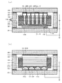
【0005】
この問題を解決するため、スピント型電子源に代わる電界放出型電子源としてカーボンナノチューブを用いたFEDが提案されている(特開平11−162383)。このカーボンナノチューブを用いたFEDは、図4に示すように、基板201上に、電極配線層202が形成され、この電極配線層202上に絶縁膜203が形成されている。この絶縁膜203上には、基板側支持リブ204が所定間隔で配置されている。そして、基板側支持リブ204で挟まれた絶縁膜203上に、所定の間隔を開けて電子放出部205が形成されている。この電子放出部205は、絶縁膜203に形成されたスルーホールを介して電極配線層202のいずれかの配線に接続している。また、図4(a)に示すように、基板側支持リブ204上には、電子引き出し電極206が形成されている。
【0006】
また、透明な前面ガラス基板207が基板201に対向配置しており、この前面ガラス基板207と基板201とは、基板側支持リブ204とこの基板側支持リブ204に直交して並べられている前面支持リブ208により、所定の距離離れて配置されている。この前面ガラス基板207と基板201との間は、真空排気されている。そして、前面ガラス基板207の内側表面の前面支持リブ208に挟まれた領域に、蛍光体からなる発光部210がストライプ形状に形成され、その表面にはアルミニウム膜を蒸着することで形成されたメタルバック膜211が形成されている。この発光部210を構成する蛍光体には、CRTなどに用いられる、4〜10KeVと高いエネルギーで加速した電子を衝突させることで発光する蛍光体が用いられている。
【0007】
以上に説明した構成において、メタルバック膜211に正の電位が印加され、また、電子引き出し電極206に正の電位が印加された状態で、電極配線層202の所定の配線に負の電位を印加することで、その配線に接続している電子放出部205から電子が放出される。そして、その放出された電子が、その電子放出部205に対向する位置の発光部210部分に到達することにより、発光部210のその部分が発光することになる。そして、ストライプ状に複数配列された発光部210に対向し、図4(c)に示すように、複数の電子放出部205がマトリクス状に配列されて、平面ディスプレイを構成するようにしている。
【0008】
【発明が解決しようとする課題】
しかしながら、前述した平面ディスプレイでは、輝度を上げるために蛍光面の加速電圧を高くする場合、絶縁破壊による放電を防ぐために電子放出部と発光部間の距離を大きくする必要があり、厚膜印刷による前面支持リブの形成が困難となっていた。例えば、加速電圧を6KVとする場合、前面支持リブの高さとして3mm程度が必要となる。これを厚膜印刷で行うと、1回の印刷でできる厚さは20μm程度のため150回の印刷が必要となり、実用的でなかった。
この発明は、以上のような問題点を解消するためになされたものであり、生産が容易で表示面積の広い薄型平面ディスプレイを提供することを目的とする。
【0009】
【課題を解決するための手段】
上述した課題を解決するために、この発明の平面ディスプレイは、少なくとも一部が透光性を有する表示面及びこの表示面に対向配置された基板を含みかつ内部が真空排気された外囲器と、この外囲器内に設けられた選択的に発光表示される蛍光体膜と、外囲器内に表示面と基板とを所定の間隔に離間するための支持構造体とを備えており、この支持構造体は複数の基板側支持リブと少なくとも1つの中間支持基板と複数の前面支持リブとから構成され、基板側支持リブは基板面から表示面側に垂設され、前面支持リブは表示面から基板側に垂設され、中間支持基板は複数のスリットが設けられて基板側支持リブと前面支持リブとの間に配置され、大気圧によりこれらのリブに挟まれて固定されていることによって特徴づけられる。
【0010】
この場合、支持構造体の一構成例は、基板側支持リブが所定の間隔で平行して配置され、前面支持リブが基板側支持リブと直交するように所定の間隔で平行して配置されている。
また、前述した平面ディスプレイの一構成例は、基板面の基板側支持リブに挟まれた領域ごとに形成された複数の電子放出部と、表示面の前面支持リブに挟まれた領域ごとに形成された蛍光体膜とこの蛍光体膜上に配置される金属膜とからなる複数の発光部と、発光部と電子放出部との間に蛍光体膜と対向して所定の間隔で配置された電子放出部から電子を引き出すための複数の電子引き出し電極とを備えている。
【0011】
この場合、中間支持基板の一構成例は、絶縁基板で構成されている。
電子引き出し電極の一構成例は、メッシュ構造を有し、基板側支持リブと中間支持基板とに挟まれて固定されている。
電子引き出し電極の別の構成例は、メッシュ構造を有し、重ねられた中間支持基板の間に挟まれて固定されている。
基板側支持リブと電子引き出し電極との間に配置された中間支持基板は、スリットが電子放出部に対応して設けられ、電子引き出し電極と前面支持リブの間に配置された中間支持基板は、スリットが発光部に対応して設けられている。
【0012】
基板側支持リブと電子引き出し電極との間に配置された中間支持基板の一構成例はスリット幅が基板側支持リブの間隔より狭く構成され、電子引き出し電極と前面支持リブの間に配置された中間支持基板の一構成例はスリット幅が前面支持リブの間隔より狭く構成されている。
前述した平面ディスプレイの別の構成例は、電子引き出し電極と発光部との間に電子の動きを制御するための制御電極が配置されている。
この場合、制御電極の一構成例は、メッシュ構造を有し、中間支持基板間に挟まれて固定されている。
また、電子放出部の一構成例は、円筒状のグラファイトの層からなるカーボンナノチューブから構成されている。
【0013】
また、この発明の平面ディスプレイの一構成例は、基板上に支持構造体の一部を構成する複数の基板側支持リブと蛍光体膜を選択的に発光表示させる電子放出部とを厚膜印刷で形成し、透明基板上に支持構造体の一部を構成する複数の前面支持リブと蛍光体膜とを厚膜印刷で形成し、支持構造体の一部を構成する少なくとも1つの絶縁基板に複数のスリットをレーザ光で形成した後、絶縁基板及び電子放出部から電子を引き出すための複数の電子引き出し電極を複数の基板側支持リブと複数の前面支持リブで挟むとともに、排気口を有するスペーサガラスを基板と透明基板の間に配置しフリットガラスで固着して外囲器を形成し、排気口を介して外囲器を真空排気して大気圧で絶縁基板を基板側支持リブと前面支持リブとで押しつけて固定した後、排気口を封着することによって製造される。
【0014】
【発明の実施の形態】
以下に図を用いてこの発明の実施の形態を説明する。
はじめに、この発明の平面ディスプレイにおける第1の実施の形態について説明する。図1は、この発明の平面ディスプレイにおける第1の実施の形態を示し、同図において(b)は断面図(a)のA−A線断面を示す。この平面ディスプレイの構成について説明すると、ガラス基板101上に基板側支持リブ104が所定間隔で垂設されており、基板側支持リブ104に挟まれたガラス基板101上に基板電極121が形成され、この基板電極121上に電子放出部120が形成されている。
【0015】
また、ガラス基板101に対向して透明なフロントガラス109が配置されており、このガラス基板101とフロントガラス109は、端部に配置された枠状のスペーサガラス108により所定の間隔で離間されている。ガラス基板101とスペーサガラス108、及びスペーサガラス108とフロントガラス109は、それぞれ低融点のフリットガラス110により接着固定されて外囲器を構成しており、外囲器内が10-3〜10-5Paの真空度に保たれている。
【0016】
この外囲器内において、フロントガラス109の内面には基板側支持リブ104と直交するように所定間隔で前面支持リブ105が垂下されており、フロントガラス109内面の前面支持リブ105に挟まれた領域に表示画素を構成する発光部が形成されている。この発光部は、フロントガラス109内面に形成された蛍光体膜と、この蛍光体膜の表面に形成されたメタルバック膜141とから構成されており、蛍光体に赤色発光蛍光体142Rを用いた赤色発光部、緑色発光蛍光体142Gを用いた緑色発光部及び青色発光蛍光体142Bを用いた青色発光部を備えている。フロントガラス109の内面は、前面支持リブ105、赤色発光部、前面支持リブ105、緑色発光部、前面支持リブ105、青色発光部の順番で所定回数分繰り返し配置され、最後の青色発光部の次に前面支持リブ105が配置された構成を有している。
【0017】
また、基板側支持リブ104上には、各発光部と1対1に対応した帯状の電子引き出し電極125が電子放出部120と直交するように所定間隔で配置されている。そして、基板側支持リブ104と前面支持リブ105と中間支持基板となる絶縁基板114とにより大気圧によるフロントガラス109とガラス基板101のたわみを所定値内にするための支持構造体が形成されている。この場合、前面支持リブ105と電子引き出し電極125の間に所定枚数の絶縁基板114が配置されており、この絶縁基板114は前面支持リブ105と電子引き出し電極125を介して基板側支持リブ104とによって挟まれ、大気圧により押しつけられて固定されている。この絶縁基板114には電子を通過させるためのスリット114aが各発光部に対応して電子放出部120と直交するように所定数設けられている。
【0018】
ここで、外囲器を構成するガラス基板101、フロントガラス109及びスペーサガラス108は、低アルカリソーダガラスを用いており、ガラス基板101とフロントガラス109は厚さ1〜2mmの板ガラスを使用する。基板電極121は、10μm程度の厚さとなるように銀あるいはカーボンを導電材料として含んだ導電性ペーストを所定のパターンでガラス基板101にスクリーン印刷した後、焼成して形成している。この場合、基板電極121は、前述した印刷で形成するものに限られるものではなく、例えば、周知のスパッタリング法とエッチング法を用いて形成された厚さ1μm程度のアルミニウム薄膜で構成してもよい。
【0019】
電子放出部120は、導電性を有する粘性溶液に複数のカーボンナノチューブが集合して構成されたバンドルを分散させたバンドルペーストを所定のパターンで基板電極121上にスクリーン印刷した後、焼成し、その後に表面をレーザ照射して表面の導電性粒子、バインダー及びバンドル中の炭素の多面体粒子を蒸発させて除去し、形成している。この電子放出部120は厚さ20〜100μmで、図2(a)に示すように、導電膜122から露出したバンドル123表面に多数のカーボンナノチューブが均一に分布しており、それぞれのカーボンナノチューブが電子放出源として動作する。
【0020】
カーボンナノチューブは、図2(b)で模式的に示すように、グラファイトの単層が円筒状に閉じ、かつ円筒の先端部に五員環が形成された構造をしており、その直径は4〜50nmと微小のため、100V程度の電界を印加することにより電子を電界放出させることができる。なお、カーボンナノチューブには、図2(b)に示した単層のものと、複数のグラファイトの層が入れ子構造的に積層し、それぞれのグラファイト層が円筒状に閉じた同軸多層構造となっているものとがあるが、どちらを用いてもよい。また、カーボンナノチューブを露出させる方法は、レーザ照射に限られるものではなく、例えばプラズマを用いた選択的なドライエッチングを用いてもよい。
【0021】
基板側支持リブ104は、電子放出部120を挟むように低融点のフリットガラスを含む絶縁ペーストを所定の高さになるまでガラス基板101上に繰り返しスクリーン印刷した後、焼成して形成した絶縁体で構成されている。この場合、基板側支持リブ104は、幅50μmで高さ200μm、リブの間隔を2.54mmとしたが、これに限られるものではなく、幅は隣接する電子放出部120間で絶縁破壊が起こらず、かつ大気圧を支えられる程度であればよく、高さは電子放出部120と電子引き出し電極125の間で放電が発生しない範囲で低くすることが望ましい。
【0022】
電子引き出し電極125は、厚さ50μmのステンレス板で構成されており、エッチングにより口径20〜100μmの多数の開口部125aが形成されている。蛍光体膜は、所定の発光色を有する蛍光体で構成されており、フロントガラス109の内面に蛍光体ペーストをストライプ状にスクリーン印刷した後、焼成して厚さ10〜100μmに形成したものである。この場合、赤(R)、緑(G)、青(B)に用いる各蛍光体142R,142G,142Bにはブラウン管等で一般的に使用されている、4〜10KeVと高いエネルギーで加速した電子を衝突させることで発光する周知の酸化物蛍光体や硫化物蛍光体を用いている。メタルバック膜141は、厚さ0.1μm程度のアルミニウム薄膜から構成されており、周知の蒸着法を用いて蛍光体膜の表面に形成されている。
【0023】
前面支持リブ105は、低融点のフリットガラスを含む絶縁ペーストを所定の高さになるまでフロントガラス109内面の所定位置に繰り返しスクリーン印刷した後、焼成して形成した絶縁体で構成されている。この場合、前面支持リブ105の幅を100〜150μm、高さを500μm、リブの間隔を1mmとした。絶縁基板114は、長さが発光部と同じで幅が0.5mmのスリット114aを1mmピッチで設けた厚さ0.3mmのアルミナ基板を用いており、スリット114aの開口はレーザ光を使用している。この場合、絶縁基板114を8枚積み重ねて2.4mmの厚さとした。
【0024】
ここでは、絶縁基板114のスリット114a幅を前面支持リブ105の間隔のおよそ1/2として発光部より狭くしたが、これは電子の通路を狭めることによりスリット114aを出てから蛍光体に到達するまでに電子が拡散する範囲を狭めて蛍光体のにじみ発光を防止する効果を考慮したものであり、そのサイズは絶縁基板114と発光部との距離や積み重ねる絶縁基板114の厚さにより最適な値を選択してよい。なお、積み重ねる絶縁基板114のスリット114a幅をすべて同じ幅としたが、必ずしも同じである必要はなく、一部あるいは全部のスリット114a幅が異なっていてもよい。また、絶縁基板114はアルミナ基板に限られるものではなく、他のセラミック基板やガラス基板を用いてもよい。また、絶縁基板114の厚さやスリット114a幅、積み重ね枚数を必要に応じて変えてよいことは言うまでもない。
【0025】
この実施の形態の平面ディスプレイは、このように構成したので、電子引き出し電極125と基板電極121の間に、電子引き出し電極125側が正の電位となるように電位差を設けることにより、電子引き出し電極125と基板電極121が交差した部分にある電子放出部120のカーボンナノチューブに電界が集中し、高電界となったカーボンナノチューブの先端から電子が放出される。このため、メタルバック膜141に正電圧(加速電圧)が印加されていると、電子放出部120から放出された電子がメタルバック膜141に向かって加速され、さらにメタルバック膜141を透過して蛍光体膜に衝突して蛍光体膜が発光させられる。
【0026】
よって、例えば、電子引き出し電極125を行方向に所定数設け、基板電極121を列方向に所定数設けて、メタルバック膜141に正電圧(加速電圧)を印加した状態で、1行目の電子引き出し電極125に所定の正電圧を印加しておいて、基板電極121に1列目から所定列目まで発光させるアドレスで所定の負電圧が印加されるように順次走査し、これを1行目から所定行目の電子引き出し電極125まで行うことにより、ドットマトリクス表示することができる。この場合、電圧を印加しない基板電極121と電子引き出し電極125は0Vにしておくか、電子引き出し電極125に基板電極121に対して数V程度の負のバイアス電圧を印加して表示アドレス以外の電子放出部120より電子が放出されないようにしておく。
【0027】
また、基板電極121に印加する電圧を0Vと正電圧とし、発光させる場合は0Vととし、発光させない場合は正電圧とするようにしてもよい。この場合、電子引き出し電極125は、アクティブな行を正電圧に保ち、他の行を0V又は数V程度の負のバイアス電圧を印加して、表示アドレス以外の電子放出部120より電子が放出されないようにしておく。この実施の形態では、メタルバック膜141に印加する電圧を6KV、電子引き出し電極125に印加する電圧を500Vと0V、基板電極121に印加する電圧を500Vと0Vとした。この場合、負電圧を用いないので負電圧電源が不要となり、コスト低減の効果が得られる。
【0028】
次に、この実施の形態の平面ディスプレイの製造方法について説明する。まず、ガラス基板101に基板電極121と電子放出部120と基板側支持リブ104とを前述した厚膜印刷の方法で形成する。次に、フロントガラス109に蛍光体膜とメタルバック膜141と前面支持リブ105とを前述した方法で形成する。また、絶縁基板114に前述した方法でスリット114aを形成する。次に、基板側支持リブが形成された面を上にしてガラス基板101を組立台に載置した後、基板側支持リブ104上に電子引き出し電極125を電子放出部120と直交するように載置する。次に、電子引き出し電極125上に所定枚数の絶縁基板114をスリット114aが電子放出部120と直交するように載置した後、ガラス基板101上の端部に枠状のスペーサガラス108を載置する。
【0029】
次に、前面支持リブ105が絶縁基板114に接触し、かつ蛍光体膜が絶縁基板114のスリット114aと対応するようにフロントガラス109をスペーサガラス108上に載置する。次に、フロントガラス109とスペーサガラス108とガラス基板101を低融点のフリットガラス110により接着固定する。次に、スペーサガラス108に設けられた排気口118を真空ポンプに接続して外囲器内を所定の圧力まで真空排気した後、排気口118を封着する。これにより、絶縁基板114が複数の基板側支持リブ104と複数の前面支持リブ105に大気圧で押しつけられて固定され、支持構造体が形成される。
【0030】
この実施の形態の平面ディスプレイによれば、支持構造体を複数の基板側支持リブ104と複数の前面支持リブ105と電子通過用スリット114aを有する所定枚数の絶縁基板114とで構成するようにしたので、繰り返し印刷して形成する前面支持リブ105の高さを低くしても、絶縁基板114を積み重ねて必要な絶縁距離を保つことができ、生産が容易になるという効果が得られる。また、大気圧による外囲器の変形が抑えられ、各電極間の距離が所定の値に保持されて発光むらが抑止できるという効果を有する。また、絶縁基板114を基板側支持リブ104と前面支持リブ105で挟み、大気圧で押しつけて固定するようにしたので、フリットガラスで固着したときに問題であった、絶縁基板114とリブの材質の違いによる熱膨張の差を原因とするクラックが生じないという効果を有する。また、絶縁基板114の厚さとスリット114a幅を最適に選ぶことにより、電子放出部120から放出された電子の拡散を抑えることができるので、隣接する画素のにじみ発光が防止できるという効果を有する。
【0031】
また、電子放出部120間に基板側支持リブ104を設けたので、隣接する電子放出部120間の漏れ電流を防ぐことができる。また、基板側支持リブ104と前面支持リブ105を直交させ、かつ電子引き出し電極125を基板側支持リブ104と直交させて配置したので、電子引き出し電極125と基板電極121の交差する部分の電子放出部120のみから電子が放出されるので、蛍光体膜や電子放出部120をマトリクス状に配置しなくともドットマトリクス表示が可能である。また、各発光部を前面支持リブ105で分離したので、隣接するR、G、B間のにじみ発光が防止できる。
【0032】
また、電子放出部120を印刷法で形成したカーボンナノチューブを含む導電膜122で構成し、これを電界放出型冷陰極電子源として用いるようにしたので、構成要素の大部分が印刷技術により形成可能であるため、非常に安価に作製することが可能となる。また、電子放出部120は、カーボンナノチューブが多数配置された状態となっているので、単位面積当たりの電子放出源の数が非常に多くなり、より多くの電子を放出させることが可能となるので、高輝度を得ることができる。また、カーボンナノチューブは化学的に安定なので放出ガスによって表面が劣化することがなく、エミッションが低下する問題も生じない。
【0033】
次に、この発明の平面ディスプレイにおける第2の実施の形態について説明する。図3は、この発明の平面ディスプレイにおける第2の実施の形態を示し、同図において(b)は断面図(a)のB−B線断面を示す。また、図1と同一符号は同一部分を示す。この平面ディスプレイが第1の実施の形態に示したものと異なる点は、電子引き出し電極125と基板側支持リブ104の間に第2の絶縁基板115を少なくとも1つ設けたことである。この場合、外囲器内に第2の絶縁基板115と電子引き出し電極125と絶縁基板114とがこの順で積み重ねられて配置され、大気圧により押しつけられた基板側支持リブ104と前面支持リブ105とに挟まれて固定されている。
【0034】
この実施の形態では、第2の絶縁基板115に電子放出部120に対応して電子引き出し電極125と直交するように電子を通過させるスリット115aが設けられている。この第2の絶縁基板115には、長さが電子放出部120と同じで幅が1.27mmのスリット115aを2.54mmピッチで設けた厚さ0.3mmのアルミナ基板を用いており、スリット115aの開口はレーザ光を使用している。この場合、第2の絶縁基板115を電子引き出し電極125と基板側支持リブ104の間に1枚配置した。
【0035】
ここでは、第2の絶縁基板115のスリット115a幅を基板側支持リブ104の間隔のおよそ1/2と電子放出部120より狭くしたが、これは電子の通路を狭めることによりスリット115aを出てから蛍光体に到達するまでに電子が拡散する範囲を狭めて、隣接する画素部分の蛍光体のにじみ発光を防止する効果を考慮したものであり、そのサイズは第2の絶縁基板115と発光部との距離や第2の絶縁基板115の厚さにより最適な値を選択してよい。なお、第2の絶縁基板115を複数積み重ねる場合、一部あるいは全部のスリット115a幅が異なっていてもよい。また、第2の絶縁基板115はアルミナ基板に限られるものではなく、他のセラミック基板やガラス基板を用いてもよい。また、第2の絶縁基板115の厚さやスリット115a幅、積み重ね枚数を必要に応じて変えてよいことは言うまでもない。
【0036】
次に、この実施の形態の平面ディスプレイの製造方法について説明する。まず、ガラス基板101に基板電極121と電子放出部120と基板側支持リブ104とを前述した厚膜印刷の方法で形成する。次に、フロントガラス109に蛍光体膜とメタルバック膜141と前面支持リブ105とを前述した方法で形成する。また、絶縁基板114と第2の絶縁基板115に前述した方法でスリット114a,115aを形成する。次に、基板側支持リブが形成された面を上にしてガラス基板101を組立台に載置した後、基板側支持リブ104上に所定枚数の第2の絶縁基板115をスリット115aが電子放出部120と対応するように載置する。
【0037】
次に、第2の絶縁基板115上に電子引き出し電極125を載置した後、電子引き出し電極125上に所定枚数の絶縁基板114を載置する。この場合、電子引き出し電極125と絶縁基板114のスリット114aが、第2の絶縁基板115のスリット115aと直交するように配置する。次に、ガラス基板101上の端部に枠状のスペーサガラス108を載置した後、前面支持リブ105が絶縁基板114に接触し、かつ蛍光体膜が絶縁基板114のスリット114aと対応するようにフロントガラス109をスペーサガラス108上に載置する。次に、フロントガラス109とスペーサガラス108とガラス基板101を低融点のフリットガラス110により接着固定する。
【0038】
次に、スペーサガラス108に設けられた排気口118を真空ポンプに接続して外囲器内を所定の圧力まで真空排気した後、排気口118を封着する。これにより、絶縁基板114と第2の絶縁基板115が複数の基板側支持リブ104と複数の前面支持リブ105に大気圧で押しつけられて固定され、支持構造体が形成される。また、同時に電子引き出し電極125も固定される。なお、絶縁基板114と第2の絶縁基板115の間に電子引き出し電極125を挟んで一体化させ、組立を簡素化するようにしてもよい。この場合、絶縁基板114と第2の絶縁基板115は、それぞれ所定の枚数で一体化するとよい。
【0039】
この実施の形態では、絶縁基板114のスリット114aと第2の絶縁基板115のスリット115aが直交しているので、これらのスリット114a,115aの交差部分に電子の通路が制限されて電子の拡散を画素範囲に収められるため、隣接する画素部分の蛍光体のにじみ発光をより有効に防止する効果が得られる。また、電子引き出し電極125を第2の絶縁基板115と絶縁基板114で挟んで一体基板にすることが可能になるので、組立が容易になる効果がある。
【0040】
次に、この発明の平面ディスプレイにおける第3の実施の形態について説明する。図4は、この発明の平面ディスプレイにおける第3の実施の形態を示し、同図において(b)は断面図(a)のC−C線断面を示す。また、図1及び図2と同一符号は同一部分を示す。この平面ディスプレイが第2の実施の形態に示したものと異なる点は、電子引き出し電極125とメタルバック膜141の間に各発光部に対応した制御電極126を設けたことである。この場合、制御電極126はメッシュ構造126aを有し、その形状は発光部に対応した帯状であり、各発光部に対応した間隔で絶縁基板114に挟まれて配置されている。この制御電極126は、厚さ50μmのステンレス板で構成されており、エッチングによりメッシュ構造126aが形成されている。
【0041】
この実施の形態の平面ディスプレイは、このように構成したので、電子引き出し電極125と基板電極121の間に、電子引き出し電極125側が正の電位となるように電位差を設けることにより、電子引き出し電極125と基板電極121が交差した部分にある電子放出部120のカーボンナノチューブに電界が集中し、高電界となったカーボンナノチューブの先端から電子が放出される。放出された電子は、電子引き出し電極125より数10V高い電圧が印加された制御電極126により運動方向が制御された後、メタルバック膜141に印加された正電圧(加速電圧)によって加速され、さらにメタルバック膜141を透過して蛍光体膜に衝突して蛍光体膜が発光させられる。この実施の形態では、制御電極126に印加する電圧を電子引き出し電極125に印加する電圧より60V高い電圧に設定した。
【0042】
次に、この実施の形態の平面ディスプレイの製造方法について説明する。まず、ガラス基板101に基板電極121と電子放出部120と基板側支持リブ104とを前述した厚膜印刷の方法で形成する。次に、フロントガラス109に蛍光体膜とメタルバック膜141と前面支持リブ105とを前述した方法で形成する。また、絶縁基板114と第2の絶縁基板115に前述した方法でスリット114a,115aを形成する。次に、基板側支持リブが形成された面を上にしてガラス基板101を組立台に載置した後、基板側支持リブ104上に所定枚数の第2の絶縁基板115をスリット115aが電子放出部120と対応するように載置する。
【0043】
次に、第2の絶縁基板115上に電子引き出し電極125を載置した後、電子引き出し電極125上に所定枚数の絶縁基板114を載置する。次に、絶縁基板114上に制御電極126を載置した後、さらに所定枚数の絶縁基板114を載置する。この場合、電子引き出し電極125と絶縁基板114のスリット114aと制御電極126が、第2の絶縁基板115のスリット115aと直交するように配置する。次に、ガラス基板101上の端部に枠状のスペーサガラス108を載置した後、前面支持リブ105が絶縁基板114に接触し、かつ蛍光体膜が絶縁基板114のスリット114aと対応するようにフロントガラス109をスペーサガラス108上に載置する。次に、フロントガラス109とスペーサガラス108とガラス基板101を低融点のフリットガラス110により接着固定する。
【0044】
次に、スペーサガラス108に設けられた排気口118を真空ポンプに接続して外囲器内を所定の圧力まで真空排気した後、排気口118を封着する。これにより、絶縁基板114と第2の絶縁基板115が複数の基板側支持リブ104と複数の前面支持リブ105に大気圧で押しつけられて固定され、支持構造体が形成される。また、同時に電子引き出し電極125と制御電極126も固定される。なお、あらかじめ第2の絶縁基板115、電子引き出し電極125、絶縁基板114、制御電極126、絶縁基板114の順に積み重ねて一体化しておき、組立を簡素化するようにしてもよい。この場合、絶縁基板114と第2の絶縁基板115は、それぞれ所定の枚数で一体化するとよい。
【0045】
この実施の形態によれば、第1の実施の形態及び第2の実施の形態の効果に加え、制御電極126によって電子の運動方向が制御されるので、放出された電子が発光部に到達するまでに拡散して発光むらが生じることがないという効果が得られる。なお、この実施の形態では、第2の実施の形態に制御電極126を加えた構成で説明したが、第1の実施の形態に制御電極126を加えた構成でも制御電極126による効果が得られることは言うまでもない。
【0046】
【発明の効果】
以上説明したように、この発明の平面ディスプレイは、少なくとも一部が透光性を有する表示面及びこの表示面に対向配置された基板を含みかつ内部が真空排気された外囲器と、この外囲器内に設けられた選択的に発光表示される蛍光体膜と、外囲器内に表示面と基板とを所定の間隔に離間するための支持構造体とを備えており、この支持構造体は複数の基板側支持リブと少なくとも1つの中間支持基板と複数の前面支持リブとから構成されるようにしたので、加速電圧を高くするため電子放出部と発光部間の距離を大きくする必要がある場合でも中間支持基板を積み重ねるだけでよく、薄型で表示面積の広い平面ディスプレイを容易に生産できるという効果を有する。また、中間支持基板を基板側支持リブと前面支持リブとの間に配置し、大気圧によりこれらのリブに挟まれて固定されるようにしたので、中間支持基板とリブの材質が異なる場合でも熱膨張の差によるクラックが生じないという効果を有する。
【図面の簡単な説明】
【図1】 第1の実施の形態を示す断面図である。
【図2】 図1の電子放出部の詳細を説明する図である。
【図3】 第2の実施の形態を示す断面図である。
【図4】 第3の実施の形態を示す断面図である。
【図5】 従来の平面ディスプレイの構成を示す断面図と平面図である。
【符号の説明】
101…ガラス基板、104…基板側支持リブ、105…前面支持リブ、108…スペーサガラス、109…フロントガラス、110…フリットガラス、114,115…絶縁基板、114a,115a…スリット、118…排気口、120…電子放出部、121…基板電極、122…導電膜、123…バンドル、125…電子引き出し電極、125a…開口部、126…制御電極、126a…メッシュ構造、141…メタルバック膜、142B…青色発光蛍光体、142G…緑色発光蛍光体、142R…赤色発光蛍光体。[0001]
BACKGROUND OF THE INVENTION
The present invention relates to a flat display in which electrons emitted from a field emission electron source collide with a phosphor to emit light, and more particularly to a flat display having a small thickness and a wide display area.
[0002]
[Prior art]
The FED (Field Emission Display) is a flat panel (planar) display that emits light emitted from an electron source arranged in a two-dimensional matrix by colliding with a light emitting portion made of a phosphor formed on a counter electrode. . This FED is a kind of vacuum microdevice using a sub-micron to micron-sized micro vacuum tube, that is, a field emission cold cathode electron source. The basic configuration is the same triode as a conventional vacuum tube, but a hot cathode is not used, but a high electric field is concentrated on a sharp cathode (emitter) so that electrons are extracted by a quantum mechanical tunnel effect. The extracted electrons are accelerated by the voltage between the anode and the cathode, and collide with and excited by the phosphor film formed on the anode to emit light. The principle is the same as that of a cathode ray tube in terms of excitation light emission of a phosphor by a cathode ray.
[0003]
In a general FED configuration, an electron emission portion and a light emission portion are formed between a vacuum-exhausted front glass substrate and the substrate. In this case, an anode made of a transparent conductive material such as ITO is formed on the inner surface of the front glass substrate, and a light emitting portion made of a phosphor is formed thereon. Further, a cathode is formed on a substrate opposed to the substrate, and a micron-sized (1-2 μm) emitter having a pointed tip (Spindt type) is formed on the insulating layer. On the insulating layer, a gate electrode for extracting electrons from the emitter is formed, and these constitute a minute electron emission portion. For example, about 200 electron emission portions are integrated for one pixel composed of red, blue, and green.
[0004]
However, the conventional FED has a problem that it is very difficult to manufacture a large number of fine emitters over the entire display region because it must be formed uniformly.
For example, in the case of a display having a diagonal length of about 10 inches, the number of pixels is about 800 × 600. Therefore, in the conventional FED, as many as 200.times.800.times.600 = 96000000 emitters must be uniformly formed over the entire display area. The larger the display is, the more this number has to be increased. There is a problem that it is difficult to enlarge the screen of the conventional FED using the Spindt-type emitter.
[0005]
In order to solve this problem, an FED using carbon nanotubes as a field emission electron source instead of a Spindt type electron source has been proposed (Japanese Patent Laid-Open No. 11-162383). In the FED using carbon nanotubes, as shown in FIG. 4, an
[0006]
Further, a transparent
[0007]
In the configuration described above, a positive potential is applied to the metal back film 211 and a negative potential is applied to a predetermined wiring of the
[0008]
[Problems to be solved by the invention]
However, in the flat display described above, when the acceleration voltage of the phosphor screen is increased in order to increase the luminance, it is necessary to increase the distance between the electron emitting portion and the light emitting portion in order to prevent discharge due to dielectric breakdown. Formation of the front support ribs has been difficult. For example, when the acceleration voltage is 6 KV, about 3 mm is required as the height of the front support rib. When this is performed by thick film printing, the thickness that can be printed by one time is about 20 μm, and 150 times of printing is required, which is not practical.
The present invention has been made to solve the above-described problems, and an object thereof is to provide a thin flat display that is easy to produce and has a wide display area.
[0009]
[Means for Solving the Problems]
In order to solve the above-described problems, a flat display according to the present invention includes an envelope that includes at least a part of a light-transmitting display surface and a substrate disposed opposite to the display surface, and the inside of which is evacuated. A phosphor film that is selectively emitted and displayed provided in the envelope, and a support structure for separating the display surface and the substrate at a predetermined interval in the envelope, The support structure includes a plurality of substrate-side support ribs, at least one intermediate support substrate, and a plurality of front support ribs. The substrate-side support ribs are suspended from the substrate surface toward the display surface, and the front support ribs are displayed. The intermediate support substrate is suspended from the surface to the substrate side, and the intermediate support substrate is provided with a plurality of slits and is disposed between the substrate side support rib and the front support rib, and is fixed by being sandwiched between these ribs by atmospheric pressure. Characterized by.
[0010]
In this case, in one configuration example of the support structure, the substrate side support ribs are arranged in parallel at a predetermined interval, and the front support ribs are arranged in parallel at a predetermined interval so as to be orthogonal to the substrate side support rib. Yes.
In addition, one configuration example of the flat display described above is formed for each of the plurality of electron emission portions formed for each region sandwiched between the substrate-side support ribs on the substrate surface and for each region sandwiched between the front support ribs of the display surface. A plurality of light emitting portions each made of a phosphor film and a metal film disposed on the phosphor film, and disposed between the light emitting portion and the electron emitting portion at a predetermined interval facing the phosphor film. And a plurality of electron extraction electrodes for extracting electrons from the electron emission portion.
[0011]
In this case, one configuration example of the intermediate support substrate is configured by an insulating substrate.
One configuration example of the electron extraction electrode has a mesh structure, and is fixed by being sandwiched between a substrate side support rib and an intermediate support substrate.
Another configuration example of the electron extraction electrode has a mesh structure, and is fixed by being sandwiched between stacked intermediate support substrates.
The intermediate support substrate disposed between the substrate side support rib and the electron extraction electrode is provided with a slit corresponding to the electron emission portion, and the intermediate support substrate disposed between the electron extraction electrode and the front support rib is A slit is provided corresponding to the light emitting portion.
[0012]
One configuration example of the intermediate support substrate disposed between the substrate-side support rib and the electron extraction electrode is configured such that the slit width is narrower than the interval between the substrate-side support ribs, and is disposed between the electron extraction electrode and the front support rib. One configuration example of the intermediate support substrate is configured such that the slit width is narrower than the interval between the front support ribs.
In another configuration example of the flat display described above, a control electrode for controlling the movement of electrons is arranged between the electron extraction electrode and the light emitting unit.
In this case, one configuration example of the control electrode has a mesh structure and is fixed by being sandwiched between the intermediate support substrates.
In addition, one structural example of the electron emission portion is composed of carbon nanotubes made of a cylindrical graphite layer.
[0013]
In addition, one configuration example of the flat display of the present invention is a thick film printing on a plurality of substrate-side support ribs that constitute a part of the support structure on the substrate and an electron emission portion that selectively emits and displays the phosphor film. A plurality of front support ribs and a phosphor film that form part of the support structure are formed on the transparent substrate by thick film printing, and are formed on at least one insulating substrate that forms part of the support structure. After forming a plurality of slits with laser light, a plurality of electron extraction electrodes for extracting electrons from the insulating substrate and the electron emission portion are sandwiched between a plurality of substrate side support ribs and a plurality of front surface support ribs, and a spacer having an exhaust port Glass is placed between the substrate and the transparent substrate and fixed with frit glass to form the envelope, and the envelope is evacuated through the exhaust port to support the insulating substrate at the atmospheric pressure with the substrate side support rib and the front surface. Press and fix with ribs After it is prepared by sealing the exhaust opening.
[0014]
DETAILED DESCRIPTION OF THE INVENTION
Embodiments of the present invention will be described below with reference to the drawings.
First, a first embodiment of the flat display according to the present invention will be described. FIG. 1 shows a first embodiment of the flat display of the present invention, in which FIG. 1 (b) shows a cross-sectional view taken along line AA of FIG. Explaining the configuration of this flat display, substrate-
[0015]
In addition, a
[0016]
In this envelope,
[0017]
Further, on the substrate-
[0018]
Here, the
[0019]
The
[0020]
As schematically shown in FIG. 2B, the carbon nanotube has a structure in which a single layer of graphite is closed in a cylindrical shape, and a five-membered ring is formed at the tip of the cylinder, and its diameter is 4 Since it is as small as ˜50 nm, it is possible to emit electrons by applying an electric field of about 100 V. The carbon nanotube has a single-layer structure shown in FIG. 2 (b) and a plurality of graphite layers stacked in a nested structure, and each graphite layer has a coaxial multilayer structure closed in a cylindrical shape. Some of them may be used. The method for exposing the carbon nanotubes is not limited to laser irradiation, and for example, selective dry etching using plasma may be used.
[0021]
The substrate-
[0022]
The
[0023]
The
[0024]
Here, the width of the
[0025]
Since the flat display of this embodiment is configured as described above, by providing a potential difference between the
[0026]
Therefore, for example, in a state where a predetermined number of
[0027]
Further, the voltage applied to the
[0028]
Next, the manufacturing method of the flat display of this embodiment is demonstrated. First, the
[0029]
Next, the
[0030]
According to the flat display of this embodiment, the support structure is composed of a plurality of substrate-
[0031]
In addition, since the substrate-
[0032]
In addition, since the
[0033]
Next, a second embodiment of the flat display according to the present invention will be described. FIG. 3 shows a second embodiment of the flat display according to the present invention, in which (b) shows a cross section taken along line BB of the cross sectional view (a). 1 denote the same parts. The flat display differs from that shown in the first embodiment in that at least one second insulating
[0034]
In this embodiment, the second insulating
[0035]
Here, the width of the
[0036]
Next, the manufacturing method of the flat display of this embodiment is demonstrated. First, the
[0037]
Next, after the
[0038]
Next, the
[0039]
In this embodiment, since the
[0040]
Next, a third embodiment of the flat display according to the present invention will be described. FIG. 4 shows a third embodiment of the flat display of the present invention, in which FIG. 4 (b) shows a cross section taken along the line C-C of the sectional view (a). 1 and 2 indicate the same parts. This flat display is different from that shown in the second embodiment in that a
[0041]
Since the flat display of this embodiment is configured as described above, by providing a potential difference between the
[0042]
Next, the manufacturing method of the flat display of this embodiment is demonstrated. First, the
[0043]
Next, after the
[0044]
Next, the
[0045]
According to this embodiment, in addition to the effects of the first embodiment and the second embodiment, the movement direction of electrons is controlled by the
[0046]
【The invention's effect】
As described above, the flat display according to the present invention includes an envelope that includes at least a part of a translucent display surface and a substrate disposed opposite to the display surface and is evacuated. A phosphor film that is selectively emitted and displayed provided in the envelope, and a support structure for separating the display surface and the substrate at a predetermined interval in the envelope. Since the body is composed of a plurality of substrate side support ribs, at least one intermediate support substrate, and a plurality of front surface support ribs, it is necessary to increase the distance between the electron emitting portion and the light emitting portion in order to increase the acceleration voltage. Even in the case where there is, there is an effect that it is only necessary to stack the intermediate support substrates, and it is possible to easily produce a flat display having a thin and wide display area. In addition, since the intermediate support substrate is disposed between the substrate side support rib and the front support rib and is fixed by being sandwiched between these ribs by atmospheric pressure, even if the material of the intermediate support substrate and the rib is different It has the effect that cracks due to differences in thermal expansion do not occur.
[Brief description of the drawings]
FIG. 1 is a cross-sectional view showing a first embodiment.
FIG. 2 is a diagram for explaining details of an electron emission unit in FIG. 1;
FIG. 3 is a cross-sectional view showing a second embodiment.
FIG. 4 is a cross-sectional view showing a third embodiment.
FIG. 5 is a cross-sectional view and a plan view showing a configuration of a conventional flat display.
[Explanation of symbols]
DESCRIPTION OF
Claims (12)
前記外囲器内に前記表示面と前記基板とを所定の間隔に離間するための支持構造体を有し、
前記支持構造体は、複数の基板側支持リブと、少なくとも1つの中間支持基板と、複数の前面支持リブとから構成され、
前記基板側支持リブは、前記基板面から前記表示面側に垂設され、
前記前面支持リブは、前記表示面から前記基板側に垂設され、
前記中間支持基板は、複数のスリットが設けられて前記基板側支持リブと前記前面支持リブとの間に配置され、大気圧によりこれらのリブに挟まれて固定されている
ことを特徴とする平面ディスプレイ。An envelope including at least a part having a light-transmitting display surface and a substrate disposed opposite to the display surface, and the inside of which is evacuated, and selectively emitting and displaying the light provided in the envelope. In a flat display with a phosphor film,
A support structure for separating the display surface and the substrate at a predetermined interval in the envelope;
The support structure includes a plurality of substrate-side support ribs, at least one intermediate support substrate, and a plurality of front support ribs.
The substrate side support rib is suspended from the substrate surface to the display surface side,
The front support rib is suspended from the display surface to the substrate side,
The intermediate support substrate is provided with a plurality of slits, is disposed between the substrate-side support ribs and the front support ribs, and is fixed by being sandwiched between the ribs by atmospheric pressure. display.
前記前面支持リブは、前記基板側支持リブと直交するように所定の間隔で平行して配置されている
ことを特徴とする請求項1記載の平面ディスプレイ。The substrate side support ribs are arranged in parallel at a predetermined interval,
The flat display according to claim 1, wherein the front support ribs are arranged in parallel at a predetermined interval so as to be orthogonal to the substrate-side support ribs.
前記表示面の前記前面支持リブに挟まれた領域ごとに形成された前記蛍光体膜とこの蛍光体膜上に形成された金属膜とからなる複数の発光部と、
前記発光部と前記電子放出部との間に前記蛍光体膜と対向して所定の間隔で配置された前記電子放出部から電子を引き出すための複数の電子引き出し電極と
を備えていることを特徴とする請求項2記載の平面ディスプレイ。A plurality of electron emission portions formed for each region sandwiched between the substrate-side support ribs of the substrate surface;
A plurality of light-emitting portions comprising the phosphor film formed for each region sandwiched between the front support ribs of the display surface and a metal film formed on the phosphor film;
A plurality of electron extraction electrodes for extracting electrons from the electron emission portion disposed at a predetermined interval facing the phosphor film between the light emitting portion and the electron emission portion. The flat display according to claim 2.
ことを特徴とする請求項1から3のいずれかに記載の平面ディスプレイ。The flat display according to claim 1, wherein the intermediate support substrate is made of an insulator.
メッシュ構造を有し、前記基板側支持リブと前記中間支持基板とに挟まれて固定されている
ことを特徴とする請求項4に記載の平面ディスプレイ。The electron extraction electrode is
5. The flat display according to claim 4, wherein the flat display has a mesh structure and is sandwiched and fixed between the substrate-side support rib and the intermediate support substrate.
メッシュ構造を有し、重ねられた前記中間支持基板の間に挟まれて固定されている
ことを特徴とする請求項4に記載の平面ディスプレイ。The electron extraction electrode is
5. The flat display according to claim 4, wherein the flat display has a mesh structure and is sandwiched and fixed between the stacked intermediate support substrates.
ことを特徴とする請求項5又は6に記載の平面ディスプレイ。The intermediate support substrate disposed between the substrate-side support rib and the electron extraction electrode is provided with a slit corresponding to the electron emission portion, and is disposed between the electron extraction electrode and the front support rib. The flat display according to claim 5 or 6, wherein the intermediate support substrate is provided with a slit corresponding to the light emitting portion.
ことを特徴とする請求項7に記載の平面ディスプレイ。The intermediate support substrate disposed between the substrate side support rib and the electron extraction electrode is configured such that the slit width is narrower than the interval between the substrate side support ribs, and is disposed between the electron extraction electrode and the front surface support rib. The flat display according to claim 7, wherein the intermediate support substrate is configured such that a slit width is narrower than an interval between the front support ribs.
ことを特徴とする請求項3から8のいずれかに記載の平面ディスプレイ。The flat display according to any one of claims 3 to 8, wherein a control electrode for controlling movement of electrons is disposed between the electron extraction electrode and the light emitting unit.
メッシュ構造を有し前記中間支持基板間に挟まれて固定されている
ことを特徴とする請求項9に記載の平面ディスプレイ。The control electrode is
The flat display according to claim 9, wherein the flat display has a mesh structure and is sandwiched and fixed between the intermediate support substrates.
円筒状のグラファイトの層からなるカーボンナノチューブから構成されていることを特徴とする請求項3から10のいずれかに記載の平面ディスプレイ。The electron emission portion is
The flat display according to any one of claims 3 to 10, wherein the flat display is composed of carbon nanotubes made of a cylindrical graphite layer.
前記基板上に前記支持構造体の一部を構成する複数の基板側支持リブと前記蛍光体膜を選択的に発光表示させる電子放出部とを厚膜印刷で形成し、透明基板上に前記支持構造体の一部を構成する複数の前面支持リブと前記蛍光体膜とを厚膜印刷で形成し、前記支持構造体の一部を構成する少なくとも1つの絶縁基板に複数のスリットをレーザ光で形成した後、前記絶縁基板及び前記電子放出部から電子を引き出すための複数の電子引き出し電極を複数の前記基板側支持リブと複数の前記前面支持リブで挟むとともに、排気口を有するスペーサガラスを前記基板と前記透明基板の間に配置しフリットガラスで固着して前記外囲器を形成し、前記排気口を介して前記外囲器を真空排気して大気圧で前記絶縁基板を前記基板側支持リブと前記前面支持リブとで押しつけて固定した後、前記排気口を封着することを特徴とする平面ディスプレイの製造方法。An envelope including at least a part of a light-transmitting display surface and a substrate disposed opposite to the display surface, the phosphor film selectively emitting and displaying, and the display surface and the substrate are predetermined. In the manufacturing method of the flat display in which the support structure for separating the gap is provided in the envelope,
A plurality of substrate-side support ribs constituting a part of the support structure and an electron emission portion for selectively emitting and displaying the phosphor film are formed on the substrate by thick film printing, and the support is formed on a transparent substrate. A plurality of front support ribs constituting a part of the structure and the phosphor film are formed by thick film printing, and a plurality of slits are formed by laser light on at least one insulating substrate constituting a part of the support structure. After the formation, a plurality of electron extraction electrodes for extracting electrons from the insulating substrate and the electron emission portion are sandwiched between the plurality of substrate side support ribs and the plurality of front surface support ribs, and a spacer glass having an exhaust port is provided. The envelope is formed by being placed between a substrate and the transparent substrate and fixed by frit glass, and the envelope is evacuated through the exhaust port to support the insulating substrate at the atmospheric pressure. Ribs and front support After fixing pressed by the ribs, manufacturing method of a flat display, characterized in that to seal the exhaust opening.
Priority Applications (1)
| Application Number | Priority Date | Filing Date | Title |
|---|---|---|---|
| JP33279199A JP4132502B2 (en) | 1999-11-24 | 1999-11-24 | Flat display and manufacturing method thereof |
Applications Claiming Priority (1)
| Application Number | Priority Date | Filing Date | Title |
|---|---|---|---|
| JP33279199A JP4132502B2 (en) | 1999-11-24 | 1999-11-24 | Flat display and manufacturing method thereof |
Publications (2)
| Publication Number | Publication Date |
|---|---|
| JP2001155667A JP2001155667A (en) | 2001-06-08 |
| JP4132502B2 true JP4132502B2 (en) | 2008-08-13 |
Family
ID=18258858
Family Applications (1)
| Application Number | Title | Priority Date | Filing Date |
|---|---|---|---|
| JP33279199A Expired - Fee Related JP4132502B2 (en) | 1999-11-24 | 1999-11-24 | Flat display and manufacturing method thereof |
Country Status (1)
| Country | Link |
|---|---|
| JP (1) | JP4132502B2 (en) |
Families Citing this family (4)
| Publication number | Priority date | Publication date | Assignee | Title |
|---|---|---|---|---|
| JP3954002B2 (en) | 2002-12-24 | 2007-08-08 | 韓國電子通信研究院 | Field emission display |
| CN100407361C (en) * | 2004-05-21 | 2008-07-30 | 东元奈米应材股份有限公司 | Construction of field emission display having reflection layer and grid |
| CN100397547C (en) * | 2004-05-21 | 2008-06-25 | 东元奈米应材股份有限公司 | Field emission display having reflection layer and grid |
| JP5074810B2 (en) * | 2007-04-18 | 2012-11-14 | トヨタ自動車株式会社 | Field emission type light emitting device |
-
1999
- 1999-11-24 JP JP33279199A patent/JP4132502B2/en not_active Expired - Fee Related
Also Published As
| Publication number | Publication date |
|---|---|
| JP2001155667A (en) | 2001-06-08 |
Similar Documents
| Publication | Publication Date | Title |
|---|---|---|
| US7153177B2 (en) | Flat-panel display and flat-panel display cathode manufacturing method | |
| JP2003263951A (en) | Field emission type electron source and driving method | |
| JP4312937B2 (en) | Fluorescent display tube | |
| JP2002025477A (en) | Surface display and its manufacturing method | |
| US7233301B2 (en) | Flat panel display and method of manufacturing the same | |
| JP4132502B2 (en) | Flat display and manufacturing method thereof | |
| JP4369075B2 (en) | Flat display | |
| KR100428037B1 (en) | Vacuum Fluorescent Display | |
| KR20050051367A (en) | Field emission display with grid plate | |
| JP2001167720A (en) | Flat-panel display | |
| JPWO2002023578A1 (en) | Display device | |
| KR20020018266A (en) | A field emission display | |
| JP3872750B2 (en) | Flat display and driving circuit | |
| JP3943001B2 (en) | Flat display and manufacturing method thereof | |
| JP2005093125A (en) | Image display device and its manufacturing method | |
| JPH07302560A (en) | Image forming device | |
| JP3564922B2 (en) | Light emitting display | |
| JP2004227822A (en) | Image display apparatus | |
| WO2006006470A1 (en) | Image display device | |
| JP2000285834A (en) | Flat-panel display | |
| JP2001143619A (en) | Method for forming rib structure and method for manufacturing flat display | |
| JP2006024516A (en) | Picture display device | |
| KR20060001459A (en) | Electron emission device | |
| JP2010135086A (en) | Flat panel display | |
| JP2008084775A (en) | Image display device |
Legal Events
| Date | Code | Title | Description |
|---|---|---|---|
| A621 | Written request for application examination |
Free format text: JAPANESE INTERMEDIATE CODE: A621 Effective date: 20060622 |
|
| A977 | Report on retrieval |
Free format text: JAPANESE INTERMEDIATE CODE: A971007 Effective date: 20080421 |
|
| TRDD | Decision of grant or rejection written | ||
| A01 | Written decision to grant a patent or to grant a registration (utility model) |
Free format text: JAPANESE INTERMEDIATE CODE: A01 Effective date: 20080507 |
|
| A01 | Written decision to grant a patent or to grant a registration (utility model) |
Free format text: JAPANESE INTERMEDIATE CODE: A01 |
|
| A61 | First payment of annual fees (during grant procedure) |
Free format text: JAPANESE INTERMEDIATE CODE: A61 Effective date: 20080602 |
|
| FPAY | Renewal fee payment (event date is renewal date of database) |
Free format text: PAYMENT UNTIL: 20110606 Year of fee payment: 3 |
|
| R150 | Certificate of patent or registration of utility model |
Free format text: JAPANESE INTERMEDIATE CODE: R150 |
|
| LAPS | Cancellation because of no payment of annual fees |