JP4131743B2 - EL display device driving method and EL display device - Google Patents
EL display device driving method and EL display device Download PDFInfo
- Publication number
- JP4131743B2 JP4131743B2 JP2007091879A JP2007091879A JP4131743B2 JP 4131743 B2 JP4131743 B2 JP 4131743B2 JP 2007091879 A JP2007091879 A JP 2007091879A JP 2007091879 A JP2007091879 A JP 2007091879A JP 4131743 B2 JP4131743 B2 JP 4131743B2
- Authority
- JP
- Japan
- Prior art keywords
- current
- pixel
- signal line
- transistor
- display
- Prior art date
- Legal status (The legal status is an assumption and is not a legal conclusion. Google has not performed a legal analysis and makes no representation as to the accuracy of the status listed.)
- Expired - Lifetime
Links
- 238000000034 method Methods 0.000 title claims description 366
- 239000000758 substrate Substances 0.000 claims description 73
- 229910021420 polycrystalline silicon Inorganic materials 0.000 claims description 37
- 229920005591 polysilicon Polymers 0.000 claims description 37
- 239000003086 colorant Substances 0.000 claims description 36
- 239000011159 matrix material Substances 0.000 claims description 23
- 239000004065 semiconductor Substances 0.000 claims description 21
- 238000005401 electroluminescence Methods 0.000 description 421
- 235000019557 luminance Nutrition 0.000 description 184
- 230000008859 change Effects 0.000 description 131
- 239000003990 capacitor Substances 0.000 description 94
- 239000010408 film Substances 0.000 description 94
- 230000002829 reductive effect Effects 0.000 description 81
- 238000010586 diagram Methods 0.000 description 79
- 230000001276 controlling effect Effects 0.000 description 64
- 230000000875 corresponding effect Effects 0.000 description 52
- 238000005516 engineering process Methods 0.000 description 40
- 230000015572 biosynthetic process Effects 0.000 description 39
- 239000010409 thin film Substances 0.000 description 39
- 238000012545 processing Methods 0.000 description 36
- 238000006243 chemical reaction Methods 0.000 description 34
- 238000012546 transfer Methods 0.000 description 34
- 230000006870 function Effects 0.000 description 29
- 230000008569 process Effects 0.000 description 28
- 239000010410 layer Substances 0.000 description 27
- 230000015556 catabolic process Effects 0.000 description 25
- 238000009826 distribution Methods 0.000 description 25
- 230000003071 parasitic effect Effects 0.000 description 25
- 238000007789 sealing Methods 0.000 description 24
- 230000000694 effects Effects 0.000 description 20
- XUIMIQQOPSSXEZ-UHFFFAOYSA-N Silicon Chemical compound [Si] XUIMIQQOPSSXEZ-UHFFFAOYSA-N 0.000 description 19
- 230000007423 decrease Effects 0.000 description 19
- 239000004973 liquid crystal related substance Substances 0.000 description 19
- 229910052710 silicon Inorganic materials 0.000 description 19
- 239000010703 silicon Substances 0.000 description 19
- 229910052751 metal Inorganic materials 0.000 description 15
- 239000002184 metal Substances 0.000 description 15
- 238000003860 storage Methods 0.000 description 14
- 229910021417 amorphous silicon Inorganic materials 0.000 description 13
- 239000000463 material Substances 0.000 description 13
- 230000001681 protective effect Effects 0.000 description 12
- 239000011521 glass Substances 0.000 description 11
- 239000012071 phase Substances 0.000 description 11
- 238000001514 detection method Methods 0.000 description 10
- XAGFODPZIPBFFR-UHFFFAOYSA-N aluminium Chemical compound [Al] XAGFODPZIPBFFR-UHFFFAOYSA-N 0.000 description 9
- 229910052782 aluminium Inorganic materials 0.000 description 8
- 239000011347 resin Substances 0.000 description 8
- 229920005989 resin Polymers 0.000 description 8
- 230000000717 retained effect Effects 0.000 description 8
- 230000005540 biological transmission Effects 0.000 description 7
- 239000006185 dispersion Substances 0.000 description 7
- 230000033001 locomotion Effects 0.000 description 7
- 238000004519 manufacturing process Methods 0.000 description 7
- 230000002093 peripheral effect Effects 0.000 description 7
- 230000009467 reduction Effects 0.000 description 7
- 238000000137 annealing Methods 0.000 description 6
- 230000003247 decreasing effect Effects 0.000 description 6
- 230000007547 defect Effects 0.000 description 6
- 238000009792 diffusion process Methods 0.000 description 6
- 238000002474 experimental method Methods 0.000 description 6
- 238000003780 insertion Methods 0.000 description 6
- 230000037431 insertion Effects 0.000 description 6
- 230000002195 synergetic effect Effects 0.000 description 6
- 238000013461 design Methods 0.000 description 5
- 238000000605 extraction Methods 0.000 description 5
- 238000005224 laser annealing Methods 0.000 description 5
- 230000001052 transient effect Effects 0.000 description 5
- OKTJSMMVPCPJKN-UHFFFAOYSA-N Carbon Chemical compound [C] OKTJSMMVPCPJKN-UHFFFAOYSA-N 0.000 description 4
- VYZAMTAEIAYCRO-UHFFFAOYSA-N Chromium Chemical compound [Cr] VYZAMTAEIAYCRO-UHFFFAOYSA-N 0.000 description 4
- 241001475178 Dira Species 0.000 description 4
- 101100309620 Schizosaccharomyces pombe (strain 972 / ATCC 24843) sck2 gene Proteins 0.000 description 4
- BQCADISMDOOEFD-UHFFFAOYSA-N Silver Chemical compound [Ag] BQCADISMDOOEFD-UHFFFAOYSA-N 0.000 description 4
- 238000004364 calculation method Methods 0.000 description 4
- 229910052799 carbon Inorganic materials 0.000 description 4
- 229910052804 chromium Inorganic materials 0.000 description 4
- 239000011651 chromium Substances 0.000 description 4
- 238000011156 evaluation Methods 0.000 description 4
- 238000007667 floating Methods 0.000 description 4
- 239000010931 gold Substances 0.000 description 4
- 230000001678 irradiating effect Effects 0.000 description 4
- 230000035515 penetration Effects 0.000 description 4
- 230000004044 response Effects 0.000 description 4
- 230000002441 reversible effect Effects 0.000 description 4
- 229910052709 silver Inorganic materials 0.000 description 4
- 239000004332 silver Substances 0.000 description 4
- LXMSZDCAJNLERA-ZHYRCANASA-N spironolactone Chemical compound C([C@@H]1[C@]2(C)CC[C@@H]3[C@@]4(C)CCC(=O)C=C4C[C@H]([C@@H]13)SC(=O)C)C[C@@]21CCC(=O)O1 LXMSZDCAJNLERA-ZHYRCANASA-N 0.000 description 4
- 208000026082 sterile multifocal osteomyelitis with periostitis and pustulosis Diseases 0.000 description 4
- 230000001360 synchronised effect Effects 0.000 description 4
- LYCAIKOWRPUZTN-UHFFFAOYSA-N Ethylene glycol Chemical compound OCCO LYCAIKOWRPUZTN-UHFFFAOYSA-N 0.000 description 3
- PXHVJJICTQNCMI-UHFFFAOYSA-N Nickel Chemical compound [Ni] PXHVJJICTQNCMI-UHFFFAOYSA-N 0.000 description 3
- 101100420795 Schizosaccharomyces pombe (strain 972 / ATCC 24843) sck1 gene Proteins 0.000 description 3
- NIXOWILDQLNWCW-UHFFFAOYSA-N acrylic acid group Chemical group C(C=C)(=O)O NIXOWILDQLNWCW-UHFFFAOYSA-N 0.000 description 3
- 230000008901 benefit Effects 0.000 description 3
- 239000013078 crystal Substances 0.000 description 3
- 239000002274 desiccant Substances 0.000 description 3
- 230000006866 deterioration Effects 0.000 description 3
- PCHJSUWPFVWCPO-UHFFFAOYSA-N gold Chemical compound [Au] PCHJSUWPFVWCPO-UHFFFAOYSA-N 0.000 description 3
- 229910052737 gold Inorganic materials 0.000 description 3
- 238000010030 laminating Methods 0.000 description 3
- 238000007726 management method Methods 0.000 description 3
- 239000003550 marker Substances 0.000 description 3
- 230000003287 optical effect Effects 0.000 description 3
- 238000000926 separation method Methods 0.000 description 3
- XOLBLPGZBRYERU-UHFFFAOYSA-N tin dioxide Chemical compound O=[Sn]=O XOLBLPGZBRYERU-UHFFFAOYSA-N 0.000 description 3
- 238000002834 transmittance Methods 0.000 description 3
- 239000004593 Epoxy Substances 0.000 description 2
- PEDCQBHIVMGVHV-UHFFFAOYSA-N Glycerine Chemical compound OCC(O)CO PEDCQBHIVMGVHV-UHFFFAOYSA-N 0.000 description 2
- 206010047571 Visual impairment Diseases 0.000 description 2
- 229910045601 alloy Inorganic materials 0.000 description 2
- 239000000956 alloy Substances 0.000 description 2
- 239000011230 binding agent Substances 0.000 description 2
- 239000011248 coating agent Substances 0.000 description 2
- 238000000576 coating method Methods 0.000 description 2
- 239000002131 composite material Substances 0.000 description 2
- 238000005520 cutting process Methods 0.000 description 2
- 238000007599 discharging Methods 0.000 description 2
- 230000009977 dual effect Effects 0.000 description 2
- 230000005684 electric field Effects 0.000 description 2
- 239000003822 epoxy resin Substances 0.000 description 2
- 210000000744 eyelid Anatomy 0.000 description 2
- 229910052732 germanium Inorganic materials 0.000 description 2
- GNPVGFCGXDBREM-UHFFFAOYSA-N germanium atom Chemical compound [Ge] GNPVGFCGXDBREM-UHFFFAOYSA-N 0.000 description 2
- 239000002346 layers by function Substances 0.000 description 2
- 239000011777 magnesium Substances 0.000 description 2
- 230000014759 maintenance of location Effects 0.000 description 2
- 230000007257 malfunction Effects 0.000 description 2
- 238000005259 measurement Methods 0.000 description 2
- 238000002156 mixing Methods 0.000 description 2
- 239000011368 organic material Substances 0.000 description 2
- 238000003909 pattern recognition Methods 0.000 description 2
- 229920000647 polyepoxide Polymers 0.000 description 2
- 238000003825 pressing Methods 0.000 description 2
- 230000000630 rising effect Effects 0.000 description 2
- 239000007787 solid Substances 0.000 description 2
- 239000007790 solid phase Substances 0.000 description 2
- 230000002123 temporal effect Effects 0.000 description 2
- RICKKZXCGCSLIU-UHFFFAOYSA-N 2-[2-[carboxymethyl-[[3-hydroxy-5-(hydroxymethyl)-2-methylpyridin-4-yl]methyl]amino]ethyl-[[3-hydroxy-5-(hydroxymethyl)-2-methylpyridin-4-yl]methyl]amino]acetic acid Chemical compound CC1=NC=C(CO)C(CN(CCN(CC(O)=O)CC=2C(=C(C)N=CC=2CO)O)CC(O)=O)=C1O RICKKZXCGCSLIU-UHFFFAOYSA-N 0.000 description 1
- 239000004925 Acrylic resin Substances 0.000 description 1
- 229920000178 Acrylic resin Polymers 0.000 description 1
- 229910000838 Al alloy Inorganic materials 0.000 description 1
- 229910001148 Al-Li alloy Inorganic materials 0.000 description 1
- JBRZTFJDHDCESZ-UHFFFAOYSA-N AsGa Chemical compound [As]#[Ga] JBRZTFJDHDCESZ-UHFFFAOYSA-N 0.000 description 1
- RYGMFSIKBFXOCR-UHFFFAOYSA-N Copper Chemical compound [Cu] RYGMFSIKBFXOCR-UHFFFAOYSA-N 0.000 description 1
- 102100040844 Dual specificity protein kinase CLK2 Human genes 0.000 description 1
- LFQSCWFLJHTTHZ-UHFFFAOYSA-N Ethanol Chemical compound CCO LFQSCWFLJHTTHZ-UHFFFAOYSA-N 0.000 description 1
- PXGOKWXKJXAPGV-UHFFFAOYSA-N Fluorine Chemical compound FF PXGOKWXKJXAPGV-UHFFFAOYSA-N 0.000 description 1
- GYHNNYVSQQEPJS-UHFFFAOYSA-N Gallium Chemical compound [Ga] GYHNNYVSQQEPJS-UHFFFAOYSA-N 0.000 description 1
- 229910001218 Gallium arsenide Inorganic materials 0.000 description 1
- 241000587161 Gomphocarpus Species 0.000 description 1
- 101000749291 Homo sapiens Dual specificity protein kinase CLK2 Proteins 0.000 description 1
- WHXSMMKQMYFTQS-UHFFFAOYSA-N Lithium Chemical compound [Li] WHXSMMKQMYFTQS-UHFFFAOYSA-N 0.000 description 1
- FYYHWMGAXLPEAU-UHFFFAOYSA-N Magnesium Chemical compound [Mg] FYYHWMGAXLPEAU-UHFFFAOYSA-N 0.000 description 1
- 206010027146 Melanoderma Diseases 0.000 description 1
- 229910000861 Mg alloy Inorganic materials 0.000 description 1
- 229910001182 Mo alloy Inorganic materials 0.000 description 1
- 239000004743 Polypropylene Substances 0.000 description 1
- RTAQQCXQSZGOHL-UHFFFAOYSA-N Titanium Chemical compound [Ti] RTAQQCXQSZGOHL-UHFFFAOYSA-N 0.000 description 1
- 230000003213 activating effect Effects 0.000 description 1
- 239000000853 adhesive Substances 0.000 description 1
- 230000001070 adhesive effect Effects 0.000 description 1
- 230000002411 adverse Effects 0.000 description 1
- 239000011324 bead Substances 0.000 description 1
- 230000002457 bidirectional effect Effects 0.000 description 1
- 230000004397 blinking Effects 0.000 description 1
- 230000000903 blocking effect Effects 0.000 description 1
- 239000004020 conductor Substances 0.000 description 1
- 229910052802 copper Inorganic materials 0.000 description 1
- 239000010949 copper Substances 0.000 description 1
- 238000012937 correction Methods 0.000 description 1
- 230000002596 correlated effect Effects 0.000 description 1
- 230000008878 coupling Effects 0.000 description 1
- 238000010168 coupling process Methods 0.000 description 1
- 238000005859 coupling reaction Methods 0.000 description 1
- 230000006378 damage Effects 0.000 description 1
- 230000002950 deficient Effects 0.000 description 1
- 238000000151 deposition Methods 0.000 description 1
- 239000003599 detergent Substances 0.000 description 1
- 230000002542 deteriorative effect Effects 0.000 description 1
- 229910003460 diamond Inorganic materials 0.000 description 1
- 239000010432 diamond Substances 0.000 description 1
- 239000007772 electrode material Substances 0.000 description 1
- 230000005674 electromagnetic induction Effects 0.000 description 1
- 238000005538 encapsulation Methods 0.000 description 1
- 239000000284 extract Substances 0.000 description 1
- 238000001914 filtration Methods 0.000 description 1
- 239000011737 fluorine Substances 0.000 description 1
- 229910052731 fluorine Inorganic materials 0.000 description 1
- 239000011888 foil Substances 0.000 description 1
- 229910052733 gallium Inorganic materials 0.000 description 1
- 238000009499 grossing Methods 0.000 description 1
- 230000012447 hatching Effects 0.000 description 1
- 230000005525 hole transport Effects 0.000 description 1
- 238000003384 imaging method Methods 0.000 description 1
- 230000006872 improvement Effects 0.000 description 1
- 229910052738 indium Inorganic materials 0.000 description 1
- APFVFJFRJDLVQX-UHFFFAOYSA-N indium atom Chemical compound [In] APFVFJFRJDLVQX-UHFFFAOYSA-N 0.000 description 1
- 229910010272 inorganic material Inorganic materials 0.000 description 1
- 239000011147 inorganic material Substances 0.000 description 1
- 238000009413 insulation Methods 0.000 description 1
- 239000011229 interlayer Substances 0.000 description 1
- 239000007788 liquid Substances 0.000 description 1
- 229910052744 lithium Inorganic materials 0.000 description 1
- 229910052749 magnesium Inorganic materials 0.000 description 1
- 239000000203 mixture Substances 0.000 description 1
- 230000004048 modification Effects 0.000 description 1
- 238000012986 modification Methods 0.000 description 1
- 229910052759 nickel Inorganic materials 0.000 description 1
- 230000000149 penetrating effect Effects 0.000 description 1
- 230000035699 permeability Effects 0.000 description 1
- 230000010363 phase shift Effects 0.000 description 1
- ISWSIDIOOBJBQZ-UHFFFAOYSA-N phenol group Chemical group C1(=CC=CC=C1)O ISWSIDIOOBJBQZ-UHFFFAOYSA-N 0.000 description 1
- 239000005011 phenolic resin Substances 0.000 description 1
- 230000001443 photoexcitation Effects 0.000 description 1
- 238000007747 plating Methods 0.000 description 1
- 229920006289 polycarbonate film Polymers 0.000 description 1
- 229920000728 polyester Polymers 0.000 description 1
- 229920006267 polyester film Polymers 0.000 description 1
- 229920001721 polyimide Polymers 0.000 description 1
- -1 polypropylene Polymers 0.000 description 1
- 229920001155 polypropylene Polymers 0.000 description 1
- 238000003672 processing method Methods 0.000 description 1
- 230000004043 responsiveness Effects 0.000 description 1
- 239000000565 sealant Substances 0.000 description 1
- 239000002356 single layer Substances 0.000 description 1
- 230000007480 spreading Effects 0.000 description 1
- 238000003892 spreading Methods 0.000 description 1
- 239000000126 substance Substances 0.000 description 1
- 230000001629 suppression Effects 0.000 description 1
- 229910001887 tin oxide Inorganic materials 0.000 description 1
- 239000010936 titanium Substances 0.000 description 1
- 229910052719 titanium Inorganic materials 0.000 description 1
- 239000005341 toughened glass Substances 0.000 description 1
- 230000007704 transition Effects 0.000 description 1
- 229910052721 tungsten Inorganic materials 0.000 description 1
Images


Description
本発明は、有機または無機エレクトロルミネッセンス(EL)素子を用いたEL表示パネルなどの自発光表示パネルに関するものである。また、これらの表示パネルの駆動回路(IC)に関するものである。EL表示パネルの駆動方法と駆動回路およびそれらを用いた情報表示装置などに関するものである。 The present invention relates to a self-luminous display panel such as an EL display panel using an organic or inorganic electroluminescence (EL) element. The present invention also relates to a drive circuit (IC) for these display panels. The present invention relates to a driving method and a driving circuit of an EL display panel, an information display device using them, and the like.
一般に、アクティブマトリクス型表示装置では、多数の画素をマトリクス状に並べ、与えられた映像信号に応じて画素毎に光強度を制御することによって画像を表示する。たとえば、電気光学物質として液晶を用いた場合は、各画素に書き込まれる電圧に応じて画素の透過率が変化する。電気光学変換物質として有機エレクトロルミネッセンス(EL)材料を用いたアクティブマトリクス型の画像表示装置は画素に書き込まれる電流に応じて発光輝度が変化する。 In general, in an active matrix display device, an image is displayed by arranging a large number of pixels in a matrix and controlling the light intensity for each pixel in accordance with a given video signal. For example, when liquid crystal is used as the electro-optical material, the transmittance of the pixel changes according to the voltage written to each pixel. In an active matrix image display device using an organic electroluminescence (EL) material as an electro-optic conversion substance, light emission luminance changes according to a current written to a pixel.
液晶表示パネルは、各画素はシャッタとして動作し、バックライトからの光を画素であるシャッタでオンオフさせることにより画像を表示する。有機EL表示パネルは各画素に発光素子を有する自発光型である。そのため、有機EL表示パネルは、液晶表示パネルに比べて画像の視認性が高い、バックライトが不要、応答速度が速い等の利点を有する。 In the liquid crystal display panel, each pixel operates as a shutter, and an image is displayed by turning on and off light from a backlight with a shutter that is a pixel. The organic EL display panel is a self-luminous type having a light emitting element in each pixel. Therefore, the organic EL display panel has advantages such as higher image visibility than the liquid crystal display panel, no backlight, and high response speed.
有機EL表示パネルは各発光素子(画素)の輝度は電流量によって制御される。つまり、発光素子が電流駆動型あるいは電流制御型であるという点で液晶表示パネルとは大きく異なる。 In the organic EL display panel, the luminance of each light emitting element (pixel) is controlled by the amount of current. That is, it is greatly different from the liquid crystal display panel in that the light emitting element is a current drive type or a current control type.
有機EL表示パネルも単純マトリクス方式とアクティブマトリクス方式の構成が可能である。前者は構造が単純であるものの大型かつ高精細の表示パネルの実現が困難である。しかし、安価である。後者は大型、高精細表示パネルを実現できる。しかし、制御方法が技術的に難しい、比較的高価であるという課題がある。現在では、アクティブマトリクス方式の開発が盛んに行われている。アクティブマトリクス方式は、各画素に設けた発光素子に流れる電流を画素内部に設けた薄膜トランジスタ(トランジスタ)によって制御する。 The organic EL display panel can also be configured in a simple matrix system and an active matrix system. Although the former has a simple structure, it is difficult to realize a large and high-definition display panel. However, it is cheap. The latter can realize a large, high-definition display panel. However, there is a problem that the control method is technically difficult and relatively expensive. At present, active matrix systems are actively developed. In the active matrix system, a current flowing through a light emitting element provided in each pixel is controlled by a thin film transistor (transistor) provided in the pixel.
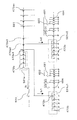
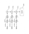
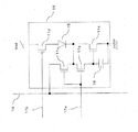
このアクティブマトリクス方式の有機EL表示パネルは、例えば、特許文献1に開示されている。この表示パネルの一画素分の等価回路を図46に示す。画素16は発光素子であるEL素子15、第1のトランジスタ11a、第2のトランジスタ11bおよび蓄積容量19からなる。発光素子15は有機エレクトロルミネッセンス(EL)素子である。本発明では、EL素子15に電流を供給(制御)するトランジスタ11aを駆動用トランジスタ11と呼ぶ。また、図46のトランジスタ11bのように、スイッチとして動作するトランジスタをスイッチ用トランジスタ11と呼ぶ。
This active matrix organic EL display panel is disclosed in
有機EL素子15は多くの場合、整流性があるため、OLED(有機発光ダイオード)と呼ばれることがある。図46などでは発光素子15としてダイオードの記号を用いている。
Since the
ただし、本発明における発光素子15はOLEDに限るものではなく、素子15に流れる電流量によって輝度が制御されるものであればよい。たとえば、無機EL素子が例示される。その他、半導体で構成される白色発光ダイオードが例示される。また、一般的な発光ダイオードが例示される。その他、発光トランジスタでもよい。また、発光素子15は必ずしも整流性が要求されるものではない。双方向性ダイオードであってもよい。本発明のEL素子15はこのいずれでもよい。
However, the
図46の例では、Pチャンネル型のトランジスタ11aのソース端子(S)をVdd(電源電位)とし、EL素子15のカソード(陰極)は接地電位(Vk)に接続される。一方、アノード(陽極)はトランジスタ11aのドレイン端子(D)に接続されている。一方、Pチャンネル型のトランジスタ11bのゲート端子はゲート信号線17aに接続され、ソース端子はソース信号線18に接続され、ドレイン端子は蓄積容量19およびトランジスタ11aのゲート端子(G)に接続されている。
In the example of FIG. 46, the source terminal (S) of the P-
画素16を動作させるために、まず、ゲート信号線17aを選択状態とし、ソース信号線18に輝度情報を表す映像信号を印加する。すると、トランジスタ11bが導通し、蓄積容量19が充電又は放電され、トランジスタ11aのゲート電位は映像信号の電位に一致する。ゲート信号線17aを非選択状態とすると、トランジスタ11aがオフになり、トランジスタ11bは電気的にソース信号線18から切り離される。しかし、トランジスタ11aのゲート電位は蓄積容量(コンデンサ)19によって安定に保持される。トランジスタ11aを介してEL素子15に流れる電流は、トランジスタ11aのゲート/ソース端子間電圧Vgsに応じた値となり、EL素子15はトランジスタ11aを通って供給される電流量に応じた輝度で発光し続ける。
In order to operate the
なお、上記の文献の全ての開示は、そっくりそのまま引用することにより、ここに一体化する。
液晶表示パネルは、自発光デバイスではないため、バックライトを用いないと画像を表示できないという問題点がある。バックライトを構成するためには所定の厚みが必要であるため、表示パネルの厚みが厚くなるという問題があった。また、液晶表示パネルでカラー表示を行うためには、カラーフィルターを使用する必要がある。そのため、光利用効率が低いという問題点があった。また、色再現範囲が狭いという問題点があった。 Since the liquid crystal display panel is not a self-luminous device, there is a problem that an image cannot be displayed unless a backlight is used. Since a predetermined thickness is required to configure the backlight, there is a problem that the thickness of the display panel is increased. In order to perform color display on the liquid crystal display panel, it is necessary to use a color filter. Therefore, there is a problem that the light utilization efficiency is low. There is also a problem that the color reproduction range is narrow.
有機EL表示パネルは、低温ポリシリコントランジスタアレイを用いてパネルを構成する。しかし、有機EL素子は、電流により発光するため、トランジスタの特性にバラツキがあると、表示ムラが発生するという課題があった。 The organic EL display panel is configured by using a low-temperature polysilicon transistor array. However, since the organic EL element emits light by current, there is a problem that display unevenness occurs when the transistor characteristics vary.
表示ムラは、画素を電流プログラム方式の構成を採用することにより低減することが可能である。電流プログラムを実施するためには、電流駆動方式のドライバ回路が必要である。しかし、電流駆動方式のドライバ回路にも電流出力段を構成するトランジスタ素子にバラツキが発生する。そのため、各出力端子からの階調出力電流にバラツキが発生し、良好な画像表示ができないという課題があった。 Display unevenness can be reduced by adopting a current programming system for the pixels. In order to implement the current program, a current drive type driver circuit is required. However, variation also occurs in the transistor elements constituting the current output stage in the current drive type driver circuit. For this reason, there is a problem in that the gradation output current from each output terminal varies and a good image display cannot be performed.
この目的を達成するために本発明のEL表示パネル(EL表示装置)のドライバ回路は、単位電流を出力する複数のトランジスタを具備し、このトランジスタの個数を変化させることにより出力電流を出力するものである。また、多段のカレントミラー回路で構成されたことを特徴としている。信号の受け渡しが電圧受け渡しとなるトランジスタ群は密に形成し、カレントミラー回路の群との信号の受け渡しは、電流受け渡しの構成を採用する。また、基準電流は、複数のトランジスタで行う。 In order to achieve this object, the driver circuit of the EL display panel (EL display device) of the present invention includes a plurality of transistors that output unit current, and outputs output current by changing the number of transistors. It is. Further, it is characterized by being composed of a multi-stage current mirror circuit. A transistor group in which signal transfer is voltage transfer is formed densely, and signal transfer with the current mirror circuit group adopts a current transfer configuration. The reference current is performed by a plurality of transistors.
第1の本発明は、EL素子を有し、前記EL素子に電流を供給する駆動用トランジスタと、前記電流の経路に形成されたスイッチ用トランジスタとが形成されている画素がマトリックス状に配置された表示画面を有するEL表示装置の駆動方法であって、
前記EL表示装置に入力される映像信号を前記画素の色に応じて重み付け処理して、前記表示画面で消費する消費電力を求め、
前記求めた消費電力に従って、前記表示画面における表示領域と非表示領域との割合を求め、
前記スイッチ用トランジスタをオンオフさせて、前記電流を制御して、前記表示画面に、帯状の前記非表示領域および前記表示領域を発生させ、その非表示領域および表示領域を前記表示画面の所定方向に移動させる、EL表示装置の駆動方法である。
According to a first aspect of the present invention, pixels each having an EL element and having a driving transistor for supplying current to the EL element and a switching transistor formed in the current path are arranged in a matrix. A method of driving an EL display device having a display screen,
The video signal input to the EL display device is weighted according to the color of the pixel to determine the power consumption consumed on the display screen,
According to the determined power consumption, determine the ratio of display area and non-display area on the display screen,
The switching transistor is turned on and off, the current is controlled, and the strip-like non-display area and the display area are generated on the display screen, and the non-display area and the display area are set in a predetermined direction of the display screen. This is a method for driving an EL display device to be moved.
第2の本発明は、前記非表示領域および前記表示領域は、帯状であり、画面の上下方向にフレーム周波数に同期して走査される、第1の本発明のEL表示装置の駆動方法である。 The second aspect of the present invention is the EL display device driving method according to the first aspect of the present invention, wherein the non-display area and the display area are strip-shaped and are scanned in the vertical direction of the screen in synchronization with the frame frequency. .
第3の本発明は、前記EL表示装置は、外光の明るさを検出する検出手段を備える、第1の本発明のEL表示装置の駆動方法である。 The third aspect of the present invention is the driving method of the EL display device according to the first aspect of the present invention, wherein the EL display device includes detection means for detecting the brightness of external light.
第4の本発明は、EL素子を有し、前記EL素子に電流を供給する駆動用トランジスタと、前記電流の経路に形成されたスイッチ用トランジスタとが形成されている画素がマトリックス状に配置された表示画面を有するEL表示装置であって、
3原色の映像信号を重み付け処理して、前記表示画面で消費する消費電力を求める演算回路と、
前記演算回路で求めた消費電力にしたがって、前記表示画面に発生させる表示領域と非表示領域との割合を変化させる表示制御回路と、
前記スイッチ用トランジスタをオンオフさせて、前記電流を制御し、前記表示画面に帯状の前記非表示領域および前記表示領域を発生させ、その非表示領域および表示領域を前記表示画面の所定方向に移動させる駆動回路とを備えたEL表示装置である。
According to a fourth aspect of the present invention, pixels each having an EL element and having a driving transistor for supplying current to the EL element and a switching transistor formed in the current path are arranged in a matrix. An EL display device having a display screen,
An arithmetic circuit for weighting the three primary color video signals to obtain power consumption consumed by the display screen;
A display control circuit that changes a ratio of a display area to be generated on the display screen and a non-display area according to the power consumption obtained by the arithmetic circuit;
The switching transistor is turned on and off to control the current, to generate the strip-like non-display area and the display area on the display screen, and to move the non-display area and the display area in a predetermined direction of the display screen An EL display device including a drive circuit.
第5の本発明は、前記EL素子が形成された基板に形成された選択回路と、
ソースドライバ回路とを更に備え、
前記ソースドライバ回路は、信号出力端子から前記3原色の映像信号を出力し、
前記基板には、前記ソースドライバ回路の前記映像信号を前記画素に伝達するソース信号線が形成され、
前記選択回路は、前記ソースドライバ回路の信号出力端子に接続する入力端子と、前記ソース信号線に接続する選択出力端子とを有し、
前記選択回路は、1つの前記入力端子と、前記入力端子に接続できる複数の選択出力端子とからなる組を複数有しており、
前記選択回路は、前記入力端子に印加された前記ソースドライバ回路の映像信号を、前記複数の選択出力端子から1つ以上を選択して、前記選択した選択出力端子に接続されたソース信号線に印加する、第4の本発明のEL表示装置である。
According to a fifth aspect of the present invention, there is provided a selection circuit formed on a substrate on which the EL element is formed,
A source driver circuit,
The source driver circuit outputs the video signals of the three primary colors from a signal output terminal;
A source signal line for transmitting the video signal of the source driver circuit to the pixel is formed on the substrate,
The selection circuit has an input terminal connected to a signal output terminal of the source driver circuit, and a selection output terminal connected to the source signal line,
The selection circuit has a plurality of sets including one input terminal and a plurality of selection output terminals that can be connected to the input terminal.
The selection circuit selects one or more video signals of the source driver circuit applied to the input terminal from the plurality of selection output terminals, and supplies them to a source signal line connected to the selected selection output terminal. It is the EL display device of the fourth aspect of the present invention to be applied.
第6の本発明は、前記ソースドライバ回路は、半導体からなるICチップであり、
前記選択回路は、前記基板にポリシリコン技術で形成されている、第4の本発明のEL表示装置である。
In a sixth aspect of the present invention, the source driver circuit is an IC chip made of a semiconductor.
The selection circuit is an EL display device according to a fourth aspect of the present invention, which is formed on the substrate by a polysilicon technique.
本発明のソースドライバ回路は、カントミラー回路を構成するトランジスタが隣接するように形成しているので、しきい値のずれによる出力電流のばらつきが小さく。したがって、EL表示パネルの輝度むらの発生を抑制することが可能となり、その実用的効果は大きい。 Since the source driver circuit of the present invention is formed so that the transistors constituting the cant mirror circuit are adjacent to each other, variation in output current due to a shift in threshold value is small. Therefore, it is possible to suppress the occurrence of luminance unevenness in the EL display panel, and its practical effect is great.
また、本発明の表示パネル、表示装置等は、高画質、良好な動画表示性能、低消費電力、低コスト化、高輝度化等のそれぞれの構成に応じて特徴ある効果を発揮する。 In addition, the display panel, the display device, and the like of the present invention exhibit distinctive effects according to their respective configurations such as high image quality, good moving image display performance, low power consumption, low cost, and high luminance.
なお、本発明を用いれば、低消費電力の情報表示装置などを構成できるので、電力を消費しない。また、小型軽量化できるので、資源を消費しない。また、高精細の表示パネルであっても十分に対応できる。したがって、地球環境、宇宙環境に優しいこととなる。 Note that if the present invention is used, a low power consumption information display device or the like can be configured, so that power is not consumed. Moreover, since it can be reduced in size and weight, resources are not consumed. Further, even a high-definition display panel can be sufficiently handled. Therefore, it is friendly to the global environment and space environment.
本明細書において各図面は理解を容易にまたは/および作図を容易にするため、省略または/および拡大縮小した箇所がある。たとえば、図11に図示する表示パネルの断面図では薄膜封止膜111などを十分厚く図示している。一方、図10において、封止フタ85は薄く図示している。また、省略した箇所もある。たとえば、本発明の表示パネルなどでは、反射防止のために円偏光板などの位相フィルムが必要である。しかし、本明細書の各図面では省略している。以上のことは以下の図面に対しても同様である。また、同一番号または、記号等を付した箇所は同一もしくは類似の形態もしくは材料あるいは機能もしくは動作を有する。
In the present specification, each drawing is omitted or / and enlarged or reduced for easy understanding and / or drawing. For example, in the cross-sectional view of the display panel shown in FIG. 11, the thin
なお、各図面等で説明した内容は特に断りがなくとも、他の実施例等と組み合わせることができる。たとえば、図8の表示パネルにタッチパネルなどを付加し、図157、図159から図161に図示する情報表示装置とすることができる。また、拡大レンズ1582を取り付け、ビデオカメラ(図159など参照のこと)などに用いるビューファインダ(図58を参照のこと)を構成することもできる。また、図4、図15、図18、図21、図23、図29、図30、図35、図36、図40、図41、図44、図100などで説明した本発明の駆動方法は、いずれの本発明の表示装置または表示パネルに適用することができる。
Note that the contents described in the drawings and the like can be combined with other embodiments and the like without particular notice. For example, a touch panel or the like is added to the display panel of FIG. 8, and the information display device illustrated in FIGS. 157 and 159 to 161 can be obtained. Further, a viewfinder (see FIG. 58) used for a video camera (see FIG. 159, etc.) can be configured by attaching a
なお、本明細書では、駆動用トランジスタ11、スイッチング用トランジスタ11は薄膜トランジスタとして説明するが、これに限定するものではない。薄膜ダイオード(TFD)、リングダイオードなどでも構成することができる。また、薄膜素子に限定するものではなく、シリコンウエハに形成したトランジスタでもものでもよい。アレイ基板71をシリコンウエハで形成すればよい。もちろん、FET、MOS−FET、MOSトランジスタ、バイポーラトランジスタでもよい。これらも基本的に薄膜トランジスタである。その他、バリスタ、サイリスタ、リングダイオード、ホトダオード、ホトトランジスタ、PLZT素子などでもよいことは言うまでもない。つまり、本発明のトランジスタ素子11、ゲートドライバ回路12、ソースドライバ回路14などは、これらのいずれでも使用することができる。
Note that in this specification, the driving
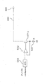
以下、本発明のELパネルについて図面を参照しながら説明をする。有機EL表示パネルは、図10に示すように、画素電極としての透明電極105が形成されたガラス板71(アレイ基板)上に、電子輸送層、発光層、正孔輸送層などからなる少なくとも1層の有機機能層(EL層)15、及び金属電極(反射膜)(カソード)106が積層されたものである。透明電極(画素電極)105である陽極(アノード)にプラス、金属電極(反射電極)106の陰極(カソード)にマイナスの電圧を加え、すなわち、透明電極105及び金属電極106間に直流を印加することにより、有機機能層(EL層)15が発光する。
Hereinafter, the EL panel of the present invention will be described with reference to the drawings. As shown in FIG. 10, the organic EL display panel includes at least one of an electron transport layer, a light emitting layer, a hole transport layer, and the like on a glass plate 71 (array substrate) on which a
金属電極106には、リチウム、銀、アルミニウム、マグネシウム、インジウム、銅または各々の合金等の仕事関数が小さなものを用いることが好ましい。特に、例えばAl−Li合金を用いることが好ましい。また、透明電極105には、ITO等の仕事関数の大きな導電性材料または金等を用いることができる。なお、金を電極材料として用いた場合、電極は半透明の状態となる。なお、ITOはIZOなどの他の材料でもよい。この事項は他の画素電極105に対しても同様である。
The
なお、封止フタ85とアレイ基板71との空間には乾燥剤107を配置する。これは、有機EL膜15は湿度に弱いためである。乾燥剤107によりシール剤を浸透する水分を吸収し有機EL膜15の劣化を防止する。
A
図10はガラスのフタ85を用いて封止する構成であるが、図11のようにフィルム(薄膜でもよい。つまり、薄膜封止膜である)111を用いた封止であってもよい。たとえば、封止フィルム(薄膜封止膜)111としては電解コンデンサのフィルムにDLC(ダイヤモンド ライク カーボン)を蒸着したものを用いることが例示される。このフィルムは水分浸透性が極めて悪い(防湿性能が高い)。このフィルムを薄膜封止膜111として用いる。また、DLC(ダイヤモンド ライク カーボン)膜などを金属電極106の表面に直接蒸着する構成でもよいことは言うまでもない。その他、樹脂薄膜と金属薄膜を多層に積層して、薄膜封止膜を構成してもよい。
FIG. 10 shows a configuration in which sealing is performed using a
薄膜の膜厚はn・d(nは薄膜の屈折率、複数の薄膜が積層されている場合はそれらの屈折率を総合(各薄膜のn・dを計算)して計算する。dは薄膜の膜厚、複数の薄膜が積層されている場合はそれらの複数の薄膜の膜厚と屈折率を総合して計算する。)が、EL素子15の発光主波長λ以下となるようにするとよい。この条件を満足させることにより、EL素子15からの光取り出し効率が、ガラス基板で封止した場合に比較して2倍以上になる。また、アルミニウムと銀の合金あるいは混合物あるいは積層物を形成してもよい。
The thickness of the thin film is calculated by n · d (where n is the refractive index of the thin film, and when a plurality of thin films are stacked, the refractive indexes thereof are combined (calculating n · d of each thin film). In the case where a plurality of thin films are laminated, the film thickness and refractive index of the plurality of thin films are comprehensively calculated.) Is preferably equal to or less than the emission main wavelength λ of the
以上のように封止フタ85を用いず、薄膜封止膜111で封止する構成を薄膜封止と呼ぶ。アレイ基板71側から光を取り出す「下取り出し(図10を参照、光取り出し方向は図10の矢印方向である)」の場合の薄膜封止は、EL膜を形成後、EL膜上にカソードとなるアルミ電極を形成する。次にこのアルミ膜上に緩衝層としての樹脂層を形成する。緩衝層としては、アクリル、エポキシなどの有機材料が例示される。また、膜厚は1μm以上10μm以下の厚みが適する。さらに好ましくは、膜厚は2μm以上6μm以下の厚みが適する。この緩衝膜(緩衝層)上に封止膜111を形成する。緩衝膜がないと、応力によりEL膜の構造が崩れ、筋状に欠陥が発生する。薄膜封止膜111は前述したように、DLC(ダイヤモンド ライク カーボン)、あるいは電界コンデンサの層構造(誘電体薄膜とアルミ薄膜とを交互に多層蒸着した構造)が例示される。
As described above, a configuration in which the sealing
EL層15側から光を取り出す「上取り出し図11を参照、光取り出し方向は図11の矢印方向である」の場合の薄膜封止は、EL膜15を形成後、EL膜15上にカソード(アノード)となるAg−Mg膜を20オングストローム以上300オングストロームの膜厚で形成する。その上に、ITOなどの透明電極を形成して低抵抗化する。次にこの電極膜上に緩衝層としての樹脂層を形成する。この緩衝膜上に薄膜封止膜111を形成する。
In the case of extracting light from the
有機EL層15から発生した光の半分は、金属電極106で反射され、アレイ基板71と透過して出射される。しかし、金属電極106は外光を反射し写り込みが発生して表示コントラストを低下させる。この対策のために、アレイ基板71にλ/4移相板108および偏光板(偏光フィルム)109を配置している。これらは一般的に円偏光板(円偏光シート)と呼ばれる。
Half of the light generated from the
なお、画素が反射電極の場合はEL層15から発生した光は上方向に出射される。したがって、位相板108および偏光板109は光出射側に配置することはいうまでもない。なお、反射型画素は、画素電極105を、アルミニウム、クロム、銀などで構成して得られる。また、画素電極105の表面に、凸部(もしくは凹凸部)を設けることで有機EL層15との界面が広くなり発光面積が大きくなり、また、発光効率が向上する。なお、カソード106(アノード105)となる反射膜を透明電極に形成する、あるいは反射率を30%以下に低減できる場合は、円偏光板は不要である。写り込みが大幅に減少するからである。また、光の干渉も低減し望ましい。
When the pixel is a reflective electrode, the light generated from the
トランジスタ11はLDD(ロー ドーピング ドレイン)構造を採用することが好ましい。また、本明細書ではEL素子として有機EL素子(OEL、PEL、PLED、OLEDなど多種多様な略称で記述される)15を例にあげて説明するがこれに限定するものではなく、無機EL素子にも適用されることは言うまでもない。
The
まず、有機EL表示パネルに用いられるアクティブマトリックス方式は、特定の画素を選択し、必要な表示情報を与えられること、1フレーム期間を通じてEL素子に電流を流すことができることという2つの条件を満足させなければならない。 First, the active matrix method used in an organic EL display panel satisfies two conditions: a specific pixel can be selected and necessary display information can be given, and a current can be passed through the EL element throughout one frame period. There must be.
この2つの条件を満足させるため、図46に図示する従来の有機ELの画素構成では、第1のトランジスタ11bは画素を選択するためのスイッチング用トランジスタ、第2のトランジスタ11aはEL素子(EL膜)15に電流を供給するための駆動用トランジスタとする。
In order to satisfy these two conditions, in the conventional organic EL pixel configuration shown in FIG. 46, the
この構成を用いて階調を表示させる場合、駆動用トランジスタ11aのゲート電圧として階調に応じた電圧を印加する必要がある。したがって、駆動用トランジスタ11aのオン電流のばらつきがそのまま表示に現れる。
In the case of displaying gradation using this configuration, it is necessary to apply a voltage corresponding to the gradation as the gate voltage of the driving
トランジスタのオン電流は単結晶で形成されたトランジスタであれば、きわめて均一であるが、安価なガラス基板に形成することのできる形成温度が450度以下の低温ポリシリ技術で形成した低温多結晶トタンジスタでは、そのしきい値のばらつきが±0.2V〜0.5Vの範囲でばらつきがある。そのため、駆動用トランジスタ11aを流れるオン電流がこれに対応してばらつき、表示にムラが発生する。これらのムラは、しきい値電圧のばらつきのみならず、トランジスタの移動度、ゲート絶縁膜の厚みなどでも発生する。また、トランジスタ11の劣化によっても特性は変化する。
The on-current of a transistor is very uniform if it is a transistor formed of a single crystal, but in a low-temperature polycrystalline transistor formed by low-temperature polysilicon technology that can be formed on an inexpensive glass substrate with a formation temperature of 450 degrees or less. The threshold value varies in the range of ± 0.2V to 0.5V. For this reason, the on-current flowing through the driving
この現象は、低温ポリシリコン技術に限定されるものではなく、プロセス温度が450度(摂氏)以上の高温ポリシリコン技術でも、固相(CGS)成長させた半導体膜を用いてトランジスタなどを形成したものでも発生する。その他、有機トランジスタでも発生する。アモルファスシリコントランジスタでも発生する。 This phenomenon is not limited to low-temperature polysilicon technology, and transistors and the like are formed using solid-phase (CGS) grown semiconductor films even in high-temperature polysilicon technology with a process temperature of 450 degrees Celsius or higher. Even things can occur. In addition, it occurs in organic transistors. It also occurs in amorphous silicon transistors.
以下に説明する本発明は、これらの技術に対応し、対策できる構成あるいは方式である。なお、本明細書では低温ポリシリコン技術で形成したトランジスタを主として説明する。 The present invention described below is a configuration or method that can cope with these techniques. In this specification, a transistor formed by low-temperature polysilicon technology will be mainly described.
したがって、図46のように、電圧を書き込むことにより、階調を表示させる方法では、均一な表示を得るために、デバイスの特性を厳密に制御する必要がある。しかし、現状の低温多結晶ポリシリコントランジスタなどではこのバラツキを所定範囲以内の抑えるというスペックを満足できない。 Therefore, as shown in FIG. 46, in the method of displaying gradation by writing a voltage, it is necessary to strictly control the device characteristics in order to obtain a uniform display. However, the current low-temperature polycrystalline polysilicon transistor and the like cannot satisfy the specification of suppressing this variation within a predetermined range.
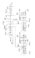
本発明のEL表示装置の画素構造は、具体的には図1に示すように単位画素が最低4つからなる複数のトランジスタ11ならびにEL素子により形成される。画素電極はソース信号線と重なるように構成する。つまり、ソース信号線18上に絶縁膜あるいはアクリル材料からなる平坦化膜を形成して絶縁し、この絶縁膜上に画素電極105を形成する。このようにソース信号線18上の少なくとも1部に画素電極を重ねる構成をハイアパーチャ(HA)構造と呼ぶ。不要な干渉光などが低減し、良好な発光状態が期待できる。
Specifically, the pixel structure of the EL display device of the present invention is formed by a plurality of
ゲート信号線(第1の走査線)17aをアクティブ(ON電圧を印加)とすることによりEL素子15の駆動用のトランジスタ11aおよびスイッチ用トランジスタ11cを通して、前記EL素子15に流すべき電流値をソースドライバ回路14から流す。また、トランジスタ11aのゲートとドレイン間を短絡するようにトランジスタ11bがゲート信号線17aアクティブ(ON電圧を印加)となることにより開くと共に、トランジスタ11aのゲートとソース間に接続されたコンデンサ(キャパシタ、蓄積容量、付加容量)19にトランジスタ11aのゲート電圧(あるいはドレイン電圧)を記憶する(図3の(a)を参照のこと)。
By activating the gate signal line (first scanning line) 17a (applying an ON voltage), the current value to be passed through the
なお、コンデンサ(蓄積容量)19の大きさは、0.2pF以上2pF以下とすることがよく、中でもコンデンサ(蓄積容量)19の大きさは、0.4pF以上1.2pF以下とすることがよい。画素サイズを考慮してコンデンサ19の容量を決定する。1画素に必要な容量をCs(pF)とし、1画素が占める面積(開口率ではない)をSp(平方μm)とすれば、500/Sp ≦ Cs ≦ 20000/Spとし、さらに好ましくは、1000/Sp ≦ Cs ≦ 10000/Spとなるようにする。なお、トランジスタのゲート容量は小さいので、ここでいうCsとは、蓄積容量(コンデンサ)19単独の容量である。
Note that the size of the capacitor (storage capacitor) 19 is preferably 0.2 pF or more and 2 pF or less, and in particular, the size of the capacitor (storage capacitor) 19 is preferably 0.4 pF or more and 1.2 pF or less. . The capacitance of the
ゲート信号線17aを非アクティブ(OFF電圧を印加)、ゲート信号線17bをアクティブとして、電流の流れる経路を前記第1のトランジスタ11a並びにEL素子15に接続されたトランジスタ11dならびに前記EL素子15を含む経路に切り替えて、記憶した電流を前記EL素子15に流すように動作する(図3の(b)を参照のこと)。
The
この回路は1画素内に4つのトランジスタ11を有しており、トランジスタ11a のゲートはトランジスタ11bのソースに接続されている。また、トランジスタ11bおよびトランジスタ11cのゲートはゲート信号線17aに接続されている。トランジスタ11bのドレインはトランジスタ11cのソースならびにトランジスタ11dのソースに接続され、トランジスタ11cのドレインはソース信号線18に接続されている。トランジスタ11dのゲートはゲート信号線17bに接続され、トランジスタ11dのドレインはEL素子15のアノード電極に接続されている。
This circuit has four
なお、図1ではすべてのトランジスタはPチャンネルで構成している。Pチャンネルは多少Nチャンネルのトランジスタに比較してモビリティが低いが、耐圧が大きくまた劣化も発生しにくいので好ましい。しかし、本発明はEL素子構成をPチャンネルで構成することのみに限定するものではない。Nチャンネルのみで構成してもよい。また、NチャンネルとPチャンネルの両方を用いて構成してもよい。 In FIG. 1, all the transistors are P-channel. The P channel has a lower mobility than an N channel transistor, but is preferable because it has a high breakdown voltage and is less likely to deteriorate. However, the present invention is not limited to the configuration of the EL element with the P channel. You may comprise only N channel. Moreover, you may comprise using both N channel and P channel.
最適には画素を構成するトランジスタ11をすべてPチャンネルで形成し、内蔵ゲートドライバ回路12もPチャンネルで形成することが好ましい。このようにアレイをPチャンネルのみのトランジスタで形成することにより、マスク枚数が5枚となり、低コスト化、高歩留まり化を実現できる。
Optimally, it is preferable that all the
以下、さらに本発明の理解を容易にするために、本発明のEL素子構成について図3を用いて説明する。本発明のEL素子構成は2つのタイミングにより制御される。第1のタイミングは必要な電流値を記憶させるタイミングである。このタイミングでトランジスタ11bならびにトランジスタ11cがONすることにより、等価回路として図3の(a)となる。ここで、信号線より所定の電流Iwが書き込まれる。これによりトランジスタ11aはゲートとドレインが接続された状態となり、このトランジスタ11aとトランジスタ11cを通じて電流Iwが流れる。したがって、トランジスタ11aのゲート−ソースの電圧はI1が流れるような電圧となる。
Hereinafter, in order to facilitate the understanding of the present invention, the EL element configuration of the present invention will be described with reference to FIG. The EL device configuration of the present invention is controlled by two timings. The first timing is a timing for storing a necessary current value. When the
第2のタイミングはトランジスタ11bとトランジスタ11cが開き、トランジスタ11dが閉じるタイミングであり、そのときの等価回路は図3の(b)となる。トランジスタ11aのソース−ゲート間の電圧は保持されたままとなる。この場合、トランジスタ11aは常に飽和領域で動作するため、Iwの電流は一定となる。
The second timing is a timing at which the
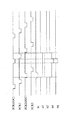
このように動作させると、図5に図示するようになる。つまり、図5の(a)の51aは表示画面50における、ある時刻での電流プログラムされている画素(行)(書き込み画素行)を示している。この画素(行)51aは、図5の(b)に図示するように非点灯(非表示画素(行))とする。他の画素(行)は表示画素(行)53とする(表示領域53の画素16のEL素子15には電流が流れ、EL素子15が発光している)。
When operated in this way, it is as shown in FIG. That is, 51a in FIG. 5A indicates a pixel (row) (write pixel row) in which current is programmed at a certain time on the
図1の画素構成の場合、図3の(a)に示すように、電流プログラム時は、プログラム電流Iwがソース信号線18に流れる。この電流Iwがトランジスタ11aを流れ、Iwを流す電流が保持されるように、コンデンサ19に電圧設定(プログラム)される。このとき、トランジスタ11dはオープン状態(オフ状態)である。
In the case of the pixel configuration of FIG. 1, as shown in FIG. 3A, the program current Iw flows through the
次に、EL素子15に電流を流す期間は図3の(b)のように、トランジスタ11c、11bがオフし、トランジスタ11dが動作する。つまり、ゲート信号線17aにオフ電圧(Vgh)が印加され、トランジスタ11b、11cがオフする。一方、ゲート信号線17bにオン電圧(Vgl)が印加され、トランジスタ11dがオンする。
Next, during a period in which a current flows through the
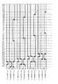
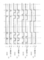
このタイミングチャートを図4に図示する。なお、図4などにおいて、括弧内の添え字(たとえば、(1)など)は画素行の番号を示している。つまり、ゲート信号線17a(1)とは、画素行(1)のゲート信号線17aを示している。また、図4の上段の*H(「*」には任意の記号、数値が当てはまり、水平走査線の番号を示す)とは、水平走査期間を示している。つまり、1Hとは第1番目の水平走査期間である。なお、以上の事項は、説明を容易にするためであって、限定(1Hの番号、1H周期、画素行番号の順番など)するものではない。
This timing chart is shown in FIG. In FIG. 4 and the like, subscripts in parentheses (for example, (1) and the like) indicate pixel row numbers. That is, the
図4でわかるように、各選択された画素行(選択期間は、1Hとしている)において、ゲート信号線17aにオン電圧が印加されている時には、ゲート信号線17bにはオフ電圧が印加されている。また、この期間は、EL素子15には電流が流れていない(非点灯状態)。選択されていない画素行において、ゲート信号線17aにオフ電圧が印加され、ゲート信号線17bにはオン電圧が印加されている。また、この期間は、EL素子15に電流が流れている(点灯状態)。
As can be seen from FIG. 4, when a turn-on voltage is applied to the
なお、トランジスタ11aのゲートとトランジスタ11cのゲートは同一のゲート信号線17aに接続している。しかし、トランジスタ11aのゲートとトランジスタ11cのゲートとを異なるゲート信号線17に接続してもよい(図32を参照のこと)。1画素のゲート信号線は3本となる(図1の構成は2本である)。トランジスタ11bのゲートのON/OFFタイミングとトランジスタ11cのゲートのON/OFFタイミングを個別に制御することにより、トランジスタ11aのばらつきによるEL素子15の電流値バラツキをさらに低減することができる。
Note that the gate of the
ゲート信号線17aとゲート信号線17bとを共通にし、トランジスタ11cと11dが異なった導電型(NチャンネルとPチャンネル)とすると、駆動回路の簡略化、ならびに画素の開口率を向上させることが出来る。
When the
このように構成すれば本発明の動作タイミングとしては信号線からの書きこみ経路がオフになる。すなわち所定の電流が記憶される際に、電流の流れる経路に分岐があると正確な電流値がトランジスタ11aのソース(S)−ゲート(G)間容量(コンデンサ)に記憶されない。トランジスタ11cとトランジスタ11dを異なった導電形にすることにより、お互いの閾値を制御することによって走査線の切り替わりのタイミングで必ずトランジスタ11cがオフしたのちに、トランジスタ11dがオンすることが可能になる。
With this configuration, the write path from the signal line is turned off as the operation timing of the present invention. That is, when a predetermined current is stored, if there is a branch in the current flow path, an accurate current value is not stored in the capacitance (capacitor) between the source (S) and the gate (G) of the
ただし、この場合お互いの閾値を正確にコントロールする必要があるのでプロセスの注意が必要である。なお、以上述べた回路は最低4つのトランジスタで実現可能であるが、より正確なタイミングのコントロールあるいは後述するように、ミラー効果低減のためにトランジスタ11eを図2に示すように、カスケード接続してトランジスタの総数が4以上になっても動作原理は同じである。このようにトランジスタ11eを加えた構成とすることにより、トランジスタ11cを介してプログラムした電流をより精度よくEL素子15に流すことができるようになる。
In this case, however, it is necessary to carefully control each other's thresholds, so care must be taken in the process. Although the circuit described above can be realized with at least four transistors, the
なお、本発明の画素構成は図1、図2の構成に限定されるものではない。たとえば、図113のように構成してもよい。図113は、図1の構成に比較してトランジスタ11dがない。替わりに切り替えスイッチ1131が形成または配置されている。図1のスイッチ11dは駆動用トランジスタ11aからEL素子15に流れる電流をオンオフ(流す、流さない)制御する機能を有する。以降の実施例でも説明をするが、本発明はこのトランジスタ11dのオンオフ制御機能が重要な構成要素である。トランジスタ11dを形成せず、オンオフ機能を実現するのが、図113の構成である。
Note that the pixel configuration of the present invention is not limited to the configurations of FIGS. For example, it may be configured as shown in FIG. 113 does not have the
図113において、切り替えスイッチ1131のa端子は、アノード電圧Vddに接続されている。なお、a端子に印加する電圧はアノード電圧Vddに限定されるものではなく、EL素子15に流れる電流をオフできる電圧であればいずれでもよい。
In FIG. 113, the terminal a of the
切り替えスイッチ1131のb端子は、カソード電圧(図113ではグランドと図示している)に接続されている。なお、b端子に印加する電圧はカソード電圧に限定されるものではなく、EL素子15に流れる電流をオンできる電圧であればいずれでもよい。
The b terminal of the
切り替えスイッチ1131のc端子にはEL素子15のカソード端子が接続されている。なお、切り替えスイッチ1131はEL素子15に流れる電流をオンオフさせる機能を持つものであればいずれでもよい。したがって、図113の形成位置に限定されるものではなく、EL素子15の電流が流れる経路であればいずれでもよい。また、スイッチの機能の限定されるものでもなく、EL素子15に流れる電流をオンオフできればいずれでもよい。つまり、本発明では、EL素子15の電流経路にEL素子15に流す電流をオンオフできるスイッチング手段を具備すればいずれの画素構成でもよい。
The cathode terminal of the
また、オフとは完全に電流が流れない状態を意味するものではない。EL素子15に流れる電流を通常よりも低減できるものであればよい。以上の事項は本発明の他の構成においても同様である。
Further, “off” does not mean a state in which no current flows completely. Any current can be used as long as the current flowing through the
切り替えスイッチ1131は、PチャンネルとNチャンネルのトランジスタを組み合わせることにより容易に実現できるので説明を要さないであろう。たとえば、アナログスイッチを2回路形成すればよい。もちろん、スイッチ1131はEL素子15に流れる電流をオンオフするだけであるから、PチャンネルトランジスタあるいはNチャンネルトランジスタでも形成することができることは言うまでもない。
Since the change-
スイッチ1131がa端子に接続されている時は、EL素子15のカソード端子にVdd電圧が印加される。したがって、駆動用トランジスタ11aのゲート端子Gがいずれの電圧保持状態であってもEL素子15には電流が流れない。したがって、EL素子15は非点灯状態となる。
When the
スイッチ1131がb端子に接続されている時は、EL素子15のカソード端子にGND電圧が印加される。したがって、駆動用トランジスタ11aのゲート端子Gに保持された電圧状態に応じてEL素子15に電流が流れる。したがって、EL素子15は点灯状態となる。
When the
以上のことより図113の画素構成では、駆動用トランジスタ11aとEL素子15間にはスイッチング用トランジスタ11dが形成されていない。しかし、スイッチ1131を制御することによりEL素子15の点灯制御を行うことができる。
From the above, in the pixel configuration of FIG. 113, the switching
図1、図2などの画素構成では、駆動用トランジスタ11aは1画素につき1個である。本発明はこれに限定するものではなく、駆動用トランジスタ11aは1画素に複数個を形成または配置してもよい。図116はその実施例である。図116では1画素に2個の駆動用トランジスタ11a1、11a2が形成され、2個の駆動用トランジスタ11a1、11a2のゲート端子は共通のコンデンサ19に接続されている。駆動用トランジスタ11aを複数個形成することにより、プログラムされる電流バラツキが低減するという効果がある。他の構成は、図1などと同様であるので説明を省略する。
In the pixel configuration shown in FIGS. 1 and 2, the number of driving
図1、図2は駆動用トランジスタ11aが出力する電流をEL素子15に流し、前記電流を駆動用トランジスタ11aとEL素子15間に配置されたトランジスタ11dでオンオフ制御するものであった。しかし、本発明はこれに限定されるものではない。たとえば、図117の構成が例示される。
1 and 2, the current output from the driving
図117の実施例では、EL素子15に流す電流が駆動用トランジスタ11aで制御される。EL素子15に流れる電流をオンオフさせるのはVdd端子とEL素子15間に配置されたスイッチング素子11dで制御される。したがって、本発明はスイッチング素子11dの配置はどこでもよく、EL素子15に流れる電流を制御できるものであればいずれでもよい。
In the embodiment of FIG. 117, the current flowing through the
トランジスタ11aの特性のバラツキはトランジスタサイズに相関がある。特性バラツキを小さくするため、第1のトランジスタ11aのチャンネル長が5μm以上100μm以下とすることが好ましい。さらに好ましくは、第1のトランジスタ11aのチャンネル長が10μm以上50μm以下とすることが好ましい。これは、チャンネル長Lを長くした場合、チャンネルに含まれる粒界が増えることによって電界が緩和されキンク効果が低く抑えられるためであると考えられる。
The variation in the characteristics of the
以上のように、本発明は、EL素子15に電流が流れこむ経路、またはEL素子15から電流が流れ出す経路(つまり、EL素子15の電流経路である)にEL素子15に流れる電流を制御する回路手段を構成または形成もしくは配置したものである。
As described above, the present invention controls the current flowing through the
電流プログラム方式の1つであるカレントミラー方式であっても、図114に図示するように、駆動用トランジスタ11bとEL素子15間にスイッチング素子としてのトランジスタ11gを形成または配置することによりEL素子15に流れる電流をオンオフすることができる(制御することができる)。もちろん、トランジスタ11gは図113のスイッチ1131に置き換えても良い。
Even in the current mirror method which is one of current programming methods, as shown in FIG. 114, by forming or arranging a
なお、図114のスイッチング用トランジスタ11d、11cは1本のゲート信号線17aに接続されているが、図115に図示するように、トランジスタ11cはゲート信号線17a1で制御し、トランジスタ11dはゲート信号線17a2で制御するように構成してもよい。図115の構成の方が、画素16の制御の汎用性が高くなる。
114 are connected to one
また、図42の(a)に図示するように、トランジスタ11b、11cなどはNチャンネルトランジスタで形成してもよい。また、図42の(b)に図示するようにトランジスタ11c、11dなどはPチャンネルトランジスタで形成してもよい。
Further, as illustrated in FIG. 42A, the
本特許の発明の目的は、トランジスタ特性のばらつきが表示に影響を与えない回路構成を提案するものであり、そのために4トランジスタ以上が必要である。これらのトランジスタ特性により、回路定数を決定する場合、4つのトランジスタの特性がそろわなければ、適切な回路定数を求めることが困難である。レーザー照射の長軸方向に対して、チャンネル方向が水平の場合と垂直の場合では、トランジスタ特性の閾値と移動度が異なって形成される。なお、どちらの場合もばらつきの程度は同じである。水平方向と、垂直方向では移動度、閾値のあたいの平均値が異なる。したがって、画素を構成するすべてのトランジスタのチャンネル方向は同一であるほうが望ましい。 The object of the invention of this patent is to propose a circuit configuration in which variations in transistor characteristics do not affect display, and for that purpose four or more transistors are required. When circuit constants are determined based on these transistor characteristics, it is difficult to obtain appropriate circuit constants if the characteristics of the four transistors do not match. When the channel direction is horizontal and vertical with respect to the major axis direction of laser irradiation, the threshold value and mobility of transistor characteristics are different. In both cases, the degree of variation is the same. The average value of mobility and threshold value differs between the horizontal direction and the vertical direction. Therefore, it is desirable that the channel directions of all the transistors constituting the pixel are the same.
また、蓄積容量19の容量値をCs(pF)、第2のトランジスタ11bのオフ電流値をIoff(pA)とした場合、次式を満足させることが好ましい。
Further, when the capacitance value of the
3 < Cs/Ioff < 24
さらに好ましくは、次式を満足させることが好ましい。
3 <Cs / Ioff <24
More preferably, it is preferable to satisfy the following formula.
6 < Cs/Ioff < 18
トランジスタ11bのオフ電流Ioffを5pA以下とすることにより、ELを流れる電流値の変化を2%以下に抑えることが可能である。これはリーク電流が増加すると、電圧非書き込み状態においてゲート−ソース間(コンデンサの両端)に貯えられた電荷を1フィールド間保持できないためである。したがって、コンデンサ19の蓄積用容量が大きければオフ電流の許容量も大きくなる。前記式を満たすことによって隣接画素間の電流値の変動を2%以下に抑えることができる。
6 <Cs / Ioff <18
By setting the off-current Ioff of the
また、アクティブマトリックスを構成するトランジスタがp−チャンネルポリシリコン薄膜トランジスタに構成され、トランジスタ11bがデュアルゲート以上であるマルチゲート構造とすることが好ましい。トランジスタ11bは、トランジスタ11aのソース−ドレイン間のスイッチとして作用するため、できるだけON/OFF比の高い特性が要求される。トランジスタ11bのゲートの構造をデュアルゲート構造以上のマルチゲート構造とすることによりON/OFF比の高い特性を実現できる。
In addition, it is preferable to adopt a multi-gate structure in which the transistors constituting the active matrix are configured as p-channel polysilicon thin film transistors and the
画素16のトランジスタ11を構成する半導体膜は、低温ポリシリコン技術において、レーザーアニールにより形成するのが一般的である。このレーザーアニールの条件のバラツキがトランジスタ11特性のバラツキとなる。しかし、1画素16内のトランジスタ11の特性が一致していれば、図1などの電流プログラムを行う方式では、所定の電流がEL素子15に流れるように駆動することができる。この点は、電圧プログラムにない利点である。レーザーとしてはエキシマレーザーを用いることが好ましい。
The semiconductor film constituting the
なお、本発明において、半導体膜の形成は、レーザーアニール方法に限定するものではなく、熱アニール方法、固相(CGS)成長による方法でもよい。その他、低温ポリシリコン技術に限定するものではなく、高温ポリシリコン技術を用いても良いことはいうまでもない。また、アモルファスシリコン技術を用いて形成した半導体膜であってもよい。 In the present invention, the formation of the semiconductor film is not limited to the laser annealing method, but may be a thermal annealing method or a method by solid phase (CGS) growth. In addition, the present invention is not limited to the low temperature polysilicon technology, and it goes without saying that the high temperature polysilicon technology may be used. Further, it may be a semiconductor film formed using amorphous silicon technology.
この課題に対して、本発明では図7に示すように、アニールの時のレーザー照射スポット(レーザー照射範囲)72をソース信号線18に平行に照射する。また、1画素列に一致するようにレーザー照射スポット72を移動させる。もちろん、1画素列に限定するものではなく、たとえば、図55のRGBを1画素16という単位でレーザーを照射してもよい(この場合は、3画素列ということになる)。また、複数の画素に同時に照射してもよい。また、レーザーの照射範囲の移動がオーバーラップしてもよいことは言うまでもない(通常、移動するレーザー光の照射範囲はオーバーラップするのが普通である)。
To deal with this problem, in the present invention, as shown in FIG. 7, a laser irradiation spot (laser irradiation range) 72 at the time of annealing is irradiated in parallel to the
画素はRGBの3画素で正方形の形状となるように作製されている。したがって、R、G、Bの各画素は縦長の画素形状となる。したがって、レーザー照射スポット72を縦長にしてアニールすることにより、1画素内ではトランジスタ11の特性バラツキが発生しないようにすることができる。また、1つのソース信号線18に接続されたトランジスタ11の特性(モビリティ、Vt、S値など)を均一にすることができる(つまり、隣接したソース信号線18のトランジスタ11とは特性が異なる場合があるが、1つのソース信号線に接続されたトランジスタ11の特性はほぼ等しくすることができる)。
The pixels are made of three pixels of RGB and have a square shape. Accordingly, each of the R, G, and B pixels has a vertically long pixel shape. Therefore, by annealing the
図7の構成では、レーザー照射スポット72の長さの範囲内に3つのパネルが縦に配置されるように形成されている。レーザー照射スポット72を照射するアニール装置はガラス基板74の位置決めマーカー73a、73bを認識(パターン認識による自動位置決め)してレーザー照射スポット72を移動させる。位置決めマーカー73の認識はパターン認識装置で行う。アニール装置(図示せず)は位置決めマーカー73を認識し、画素列の位置をわりだす(レーザー照射範囲72がソース信号線18と平行になるようにする)。画素列位置に重なるようにレーザー照射スポット72を照射してアニールを順次行う。
In the configuration of FIG. 7, three panels are formed vertically within the range of the length of the
図7で説明したレーザーアニール方法(ソース信号線18に平行にライン状のレーザースポットを照射する方式)は、有機EL表示パネルの電流プログラム方式の時に特に採用することが好ましい。なぜならば、ソース信号線に平行方向にトランジスタ11の特性が一致しているためである(縦方向に隣接した画素トランジスタの特性が近似している)。そのため、電流駆動時にソース信号線の電圧レベルの変化が少なく、電流書き込み不足が発生しにくい。
The laser annealing method described in FIG. 7 (method of irradiating a line-shaped laser spot in parallel with the source signal line 18) is preferably employed particularly in the current programming method of the organic EL display panel. This is because the characteristics of the
たとえば、白ラスター表示であれば、隣接した各画素のトランジスタ11aに流す電流はほぼ同一のため、ソースドライバIC14から出力する電流振幅の変化が少ない。もし、図1のトランジスタ11aの特性が同一であり、各画素に電流プログラムする電流値が画素列で等しいのであれば、電流プログラム時のソース信号線18の電位は一定である。したがって、ソース信号線18の電位変動は発生しない。1つのソース信号線18に接続されたトランジスタ11aの特性がほぼ同一であれば、ソース信号線18の電位変動は小さいことになる。このことは、図38などの他の電流プログラム方式の画素構成でも同一である(つまり、図7の製造方法を適用することが好ましい)。
For example, in the case of white raster display, the current flowing through the
また、図27、図30などで説明する複数の画素行を同時書き込みする方式で均一が画像表示(主としてトランジスタ特性のばらつきに起因する表示ムラが発生しにくいからである)を実現できる。図27などは複数画素行同時に選択するから、隣接した画素行のトランジスタが均一であれば、縦方向のトランジスタ特性ムラはソースドライバ回路14で吸収できる。
In addition, uniform image display (since display unevenness due to variations in transistor characteristics is unlikely to occur) can be realized by a method of simultaneously writing a plurality of pixel rows described with reference to FIGS. In FIG. 27 and the like, a plurality of pixel rows are selected simultaneously. Therefore, if the transistors in adjacent pixel rows are uniform, the transistor characteristic unevenness in the vertical direction can be absorbed by the
なお、図7では、ソースドライバ回路14は、ICチップを積載するように図示しているが、これに限定するものではなく、ソースドライバ回路14を画素16と同一プロセスで形成してもよいことは言うまでもない。
In FIG. 7, the
本発明では特に、駆動用トランジスタ11bの閾電圧Vth2が画素内で対応する駆動用トランジスタ11aの閾電圧Vth1より低くならない様に設定している。例えば、トランジスタ11bのゲート長L2をトランジスタ11aのゲート長L1よりも長くして、これらの薄膜トランジスタのプロセスパラメータが変動しても、Vth2がVth1よりも低くならない様にする。これにより、微少な電流リークを抑制することが可能である。
In the present invention, in particular, the threshold voltage Vth2 of the driving
なお、以上の事項は、図38に図示するカレントミラーの画素構成にも適用できる。図38では、信号電流が流れる駆動用トランジスタ11a、EL素子15等からなる発光素子に流れる駆動電流を制御する駆動用トランジスタ11bの他、ゲート信号線17a1の制御によって画素回路とデータ線dataとを接続もしくは遮断する取込用トランジスタ11c、ゲート信号線17a2の制御によって書き込み期間中にトランジスタ11aのゲート・ドレインを短絡するスイッチ用トランジスタ11d、トランジスタ11aのゲート−ソース間電圧を書き込み終了後も保持するための容量C19および発光素子としてのEL素子15などから構成される。
The above items can also be applied to the pixel configuration of the current mirror shown in FIG. In FIG. 38, the pixel circuit and the data line data are controlled by controlling the gate signal line 17a1 in addition to the driving
図38でトランジスタ11c、11dはNチャンネルトランジスタ、その他のトランジスタはPチャンネルトランジスタで構成しているが、これは一例であって、必ずしもこの通りである必要はない。容量Csは、その一方の端子をトランジスタ11aのゲートに接続され、他方の端子はVdd(電源電位)に接続されているが、Vddに限らず任意の一定電位でも良い。EL素子15のカソード(陰極)は接地電位に接続されている。
In FIG. 38, the
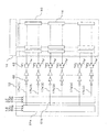
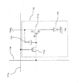
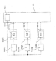
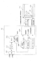
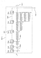
次に、本発明のEL表示パネルあるいはEL表示装置について説明をする。図6はEL表示装置の回路を中心とした説明図である。画素16がマトリックス状に配置または形成されている。各画素16には各画素の電流プログラムを行う電流を出力するソースドライバ回路14が接続されている。ソースドライバ回路14の出力段は映像信号のビット数に対応したカレントミラー回路が形成されている(後に説明する)。たとえば、64階調であれば、63個のカレントミラー回路が各ソース信号線に形成され、これらのカレントミラー回路の個数を選択することにより所望の電流をソース信号線18に印加できるように構成されている(図48を参照のこと)。
Next, the EL display panel or EL display device of the present invention will be described. FIG. 6 is an explanatory diagram focusing on the circuit of the EL display device.
なお、1つのカレントミラー回路の最小出力電流は10nA以上50nAにしている。特にカレントミラー回路の最小出力電流は15nA以上35nAにすることがよい。ソースドライバIC14内のカレントミラー回路を構成するトランジスタの精度を確保するためである。
The minimum output current of one current mirror circuit is 10 nA or more and 50 nA. In particular, the minimum output current of the current mirror circuit is preferably 15 nA or more and 35 nA. This is to ensure the accuracy of the transistors constituting the current mirror circuit in the
また、ソース信号線18の電荷を強制的に放出または充電するプリチャージあるいはディスチャージ回路を内蔵する。ソース信号線18の電荷を強制的に放出または充電するプリチャージあるいはディスチャージ回路の電圧(電流)出力値は、R、G、Bで独立に設定できるように構成することが好ましい。EL素子15の閾値がRGBで異なるからである(プリチャージ回路については図65、図67およびその説明を参照のこと)。
In addition, a precharge or discharge circuit for forcibly releasing or charging the
有機EL素子は大きな温度依存性特性(温特)があることが知られている。この温特による発光輝度変化を調整するため、カレントミラー回路に出力電流を変化させるサーミスタあるいはポジスタなどの非直線素子を付加し、温特による変化を前記サーミスタなどで調整することによりアナログ的に基準電流を調整する(変化させる)。 It is known that an organic EL element has a large temperature dependency characteristic (temperature characteristic). In order to adjust the light emission luminance change due to the temperature characteristics, a non-linear element such as a thermistor or a posistor that changes the output current is added to the current mirror circuit, and the temperature characteristics change is adjusted by the thermistor as an analog reference. Adjust (change) the current.
本発明において、ソースドライバ回路14は半導体シリコンチップで形成し、チップオンガラス(COG)技術でアレイ基板71のソース信号線18の端子と接続されている。ソースドライバ回路14の実装は、COG技術に限定するものではなく、チップオンフィルム(COF)技術に前述のソースドライバIC14などを積載し、表示パネルの信号線と接続した構成としてもよい。また、ドライブICは電源IC82を別途作製し、3チップ構成としてもよい。
In the present invention, the
一方、ゲートドライバ回路12は低温ポリシリコン技術で形成している。つまり、画素のトランジスタと同一のプロセスで形成している。これは、ソースドライバ回路14に比較して内部の構造が容易で、動作周波数も低いためである。したがって、低温ポリシリ技術で形成しても容易に形成することができ、また、狭額縁化を実現できる。もちろん、ゲートドライバ回路12をシリコンチップで形成し、COG技術などを用いてアレイ基板71上に実装してもよいことは言うまでもない。また、画素トランジスタなどのスイッチング素子、ゲートドライバなどは高温ポリシリコン技術で形成してもよく、有機材料で形成(有機トランジスタ)してもよい。
On the other hand, the
ゲートドライバ回路12はゲート信号線17a用のシフトレジスタ回路61aと、ゲート信号線17b用のシフトレジスタ回路61bとを内蔵する。各シフトレジスタ回路61は正相と負相のクロック信号(CLKxP、CLKxN)、スタートパルス(STx)で制御される(図6を参照のこと)。その他、ゲート信号線の出力、非出力を制御するイネーブル(ENABL)信号、シフト方向を上下逆転するアップダウン(UPDWM)信号を付加することが好ましい。他に、スタートパルスがシフトレジスタにシフトされ、そして出力されていることを確認する出力端子などを設けることが好ましい。なお、シフトレジスタのシフトタイミングはコントロールIC81からの制御信号で制御される。また、外部データのレベルシフトを行うレベルシフト回路を内蔵する。
The
シフトレジスタ回路61のバッファ容量は小さいため、直接にはゲート信号線17を駆動することができない。そのため、シフトレジスタ回路61の出力とゲート信号線17を駆動する出力ゲート63間には少なくとも2つ以上のインバータ回路62が形成されている。
Since the buffer capacity of the shift register circuit 61 is small, the
ソースドライバ回路14を低温ポリシリなどのポリシリ技術でアレイ基板71上に直接形成する場合も同様であり、ソース信号線18を駆動するトランスファーゲートなどのアナログスイッチのゲートとソースドライバ回路14のシフトレジスタ間には複数のインバータ回路が形成される。以下の事項(シフトレジスタの出力と、信号線を駆動する出力段(出力ゲートあるいはトランスファーゲートなどの出力段間に配置されるインバータ回路に関する事項))は、ソースドライブおよびゲートドライブ回路に共通の事項である。
The same applies to the case where the
たとえば、図6ではソースドライバ回路14の出力が直接ソース信号線18に接続されているように図示したが、実際には、ソースドライバのシフトレジスタの出力は多段のインバータ回路が接続されて、インバータの出力がトランスファーゲートなどのアナログスイッチのゲートに接続されている。
For example, FIG. 6 shows that the output of the
インバータ回路62はPチャンネルのMOSトランジスタとNチャンネルのMOSトランジスタから構成される。先にも説明したようにゲートドライバ回路12のシフトレジスタ回路61の出力端にはインバータ回路62が多段に接続されており、その最終出力が出力ゲート回路63に接続されている。なお、インバータ回路62はPチャンネルのみで構成してもよい。ただし、この場合は、インバータではなく単なるゲート回路として構成してもよい。
The
図8は本発明の表示装置の信号、電圧の供給の構成図あるいは表示装置の構成図である。コントロールIC81からソースドライバ回路14aに供給する信号(電源配線、データ配線など)はフレキシブル基板84を介して供給する。
FIG. 8 is a configuration diagram of signal and voltage supply of the display device of the present invention or a configuration diagram of the display device. Signals (power supply wiring, data wiring, etc.) supplied from the
図8ではゲートドライバ回路12の制御信号はコントロールICで発生させ、ソースドライバ回路14で、レベルシフトを行った後、ゲートドライバ回路12に印加している。ソースドライバ回路14の駆動電圧は4〜8(V)であるから、コントロールIC81から出力された3.3(V)振幅の制御信号を、ゲートドライバ回路12が受け取れる5(V)振幅に変換することができる。
In FIG. 8, the control signal of the
なお、図8などにおいて14をソースドライバと記載したが、単なるドライバだけでなく、電源回路、バッファ回路(シフトレジスタなどの回路を含む)、データ変換回路、ラッチ回路、コマンドデコーダ、シフト回路、アドレス変換回路、画像メモリなどを内蔵させてもよい。なお、図8などで説明する構成にあっても、図9などで説明する3辺フリー構成あるいは構成、駆動方式などを適用できることはいうまでもない。 8 is described as a source driver in FIG. 8 and the like, but not only a driver, but also a power supply circuit, a buffer circuit (including a circuit such as a shift register), a data conversion circuit, a latch circuit, a command decoder, a shift circuit, an address A conversion circuit, an image memory, or the like may be incorporated. Needless to say, the three-side free configuration or configuration described in FIG. 9 or the like, the driving method, or the like can be applied to the configuration described in FIG. 8 or the like.
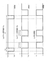
表示パネルを携帯電話などの情報表示装置に使用する場合、図9に示すように、ソースドライバIC(回路)14、ゲートドライバIC(回路)12は、表示パネルの一辺に実装(形成)することが好ましい(なお、このように一辺にドライバIC(回路)を実装(形成)する形態を3辺フリー構成(構造)と呼ぶ。従来は、表示領域のX辺にゲートドライバIC12が実装され、Y辺にソースドライバIC14が実装されていた)。画面50の中心線が表示装置の中心になるように設計し易く、また、ドライバICの実装も容易となるからである。なお、ゲートドライバ回路を高温ポリシリコンあるいは低温ポリシリコン技術などで3辺フリーの構成で作製してもよい(つまり、図9のソースドライバ回路14とゲートドライバ回路12のうち、少なくとも一方をポリシリコン技術でアレイ基板71に直接形成する)。
When the display panel is used for an information display device such as a mobile phone, as shown in FIG. 9, the source driver IC (circuit) 14 and the gate driver IC (circuit) 12 are mounted (formed) on one side of the display panel. (A configuration in which the driver IC (circuit) is mounted (formed) on one side in this way is called a three-side free configuration (structure). Conventionally, the
なお、3辺フリー構成とは、アレイ基板71に直接ICを積載あるいは形成した構成だけでなく、ソースドライバIC(回路)14、ゲートドライバIC(回路)12などを取り付けたフィルム(TCP、TAB技術など)をアレイ基板71の一辺(もしくはほぼ一辺)にはりつけた構成も含む。つまり、2辺にICが実装あるいは取り付けられていない構成、配置あるいはそれに類似するすべてを意味する。
The three-side free configuration is not only a configuration in which an IC is directly stacked or formed on the
図9のようにゲートドライバ回路12をソースドライバ回路14の横に配置すると、ゲート信号線17は辺Cにそって形成する必要がある。
When the
なお、図9などにおいて太い実線で図示した箇所はゲート信号線17が並列して形成した箇所を示している。したがって、bの部分(画面下部)は走査信号線の本数分のゲート信号線17が並列して形成され、aの部分(画面上部)はゲート信号線17が1本形成されている。
In FIG. 9 and the like, a portion indicated by a thick solid line indicates a portion where the
C辺に形成するゲート信号線17のピッチは5μm以上12μm以下にする。5μm未満では隣接ゲート信号線に寄生容量の影響によりノイズが乗ってしまう。実験によれば7μ以下で寄生容量の影響が顕著に発生する。さらに5μm未満では表示画面にビート状などの画像ノイズが激しく発生する。特にノイズの発生は画面の左右で異なり、このビート状などの画像ノイズを低減することは困難である。また、ピッチが12μmを越えると表示パネルの額縁幅Dが大きくなりすぎ実用的でない。
The pitch of the
前述の画像ノイズを低減するためには、ゲート信号線17を形成した部分の下層あるいは上層に、グランドパターン(一定電圧に電圧固定あるいは全体として安定した電位に設定されている導電パターン)を配置することにより低減できる。また、別途設けたシールド板(シールド箔(一定電圧に電圧固定あるいは全体として安定した電位に設定されている導電パターン))をゲート信号線17上に配置すればよい。
To reduce the above-described image noise, the lower layer or the upper layer of the portion to form the
図9のC辺のゲート信号線17はITO電極で形成してもよいが、低抵抗化するため、ITOと金属薄膜とを積層して形成することが好ましい。また、金属膜で形成することが好ましい。ITOと積層する場合は、ITO上にチタン膜を形成し、その上にアルミニウムあるいはアルミニウムとモリブデンの合金薄膜を形成する。もしくはITO上にクロム膜を形成する。金属膜の場合は、アルミニウム薄膜、クロム薄膜で形成する。以上の事項は本発明の他の実施例でも同様である。
Although the
なお、図9などにおいて、ゲート信号線17などは表示領域の片側に配置するとしたがこれに限定するものではなく、両方に配置してもよい。たとえば、ゲート信号線17aを表示画面50の右側に配置(形成)し、ゲート信号線17bを表示画面50の左側に配置(形成)してもよい。以上の事項は他の実施例でも同様である。
In FIG. 9 and the like, the
また、ソースドライバIC14とゲートドライバIC12とを1チップ化してもよい。1チップ化すれば、表示パネルへのICチップの実装が1個で済む。したがって、実装コストも低減できる。また、1チップドライバIC内で使用する各種電圧も同時に発生することができる。
Further, the
なお、ソースドライバIC14、ゲートドライバIC12はシリコンなどの半導体ウエハで作製し、表示パネルに実装するとしたがこれに限定するものではなく、低温ポリシリコン技術、高温ポリシリコン技術により表示パネル71に直接形成してもよいことは言うまでもない。
The
なお、画素は、R、G、Bの3原色としたがこれに限定するものではなく、シアン、イエロー、マゼンダの3色でもよい。また、Bとイエローの2色でもよい。もちろん、単色でもよい。また、R、G、B、シアン、イエロー、マゼンダの6色でもよい。R、G、B、シアン、マゼンダの5色でもよい。これらはナチュラルカラーとして色再現範囲が拡大し良好な表示を実現できる。以上のように本発明のEL表示装置は、RGBの3原色でカラー表示を行うものに限定されるものではない。 The pixels are R, G, and B primary colors. However, the present invention is not limited to this, and may be cyan, yellow, and magenta. Also, two colors of B and yellow may be used. Of course, it may be a single color. Also, six colors of R, G, B, cyan, yellow, and magenta may be used. Five colors of R, G, B, cyan, and magenta may be used. These are natural colors, and the color reproduction range is expanded to achieve a good display. As described above, the EL display device of the present invention is not limited to one that performs color display with the three primary colors RGB.
有機EL表示パネルのカラー化には主に三つの方式があり、色変換方式はこのうちの一つである。発光層として青色のみの単層を形成すればよく、フルカラー化に必要な残りの緑色と赤色は、青色光から色変換によって作り出す。したがって、RGBの各層を塗り分ける必要がない、RGBの各色の有機EL材料をそろえる必要がないという利点がある。色変換方式は、塗り分け方式のようは歩留まり低下がない。本発明のEL表示パネルなどはこのいずれの方式でも適用される。 There are mainly three methods for colorizing an organic EL display panel, and one of them is a color conversion method. It is only necessary to form a blue-only single layer as the light emitting layer, and the remaining green and red colors necessary for full color are generated from blue light by color conversion. Therefore, there is an advantage that it is not necessary to separately coat each layer of RGB, and it is not necessary to prepare organic EL materials of each color of RGB. The color conversion method does not cause a decrease in yield unlike the color separation method. The EL display panel of the present invention can be applied to any of these methods.
また、3原色の他に、白色発光の画素を形成してもよい。白色発光の画素はR、G、B発光の構造を積層することにより作製(形成または構成)することにより実現できる。1組の画素は、RGBの3原色と、白色発光の画素16Wからなる。白色発光の画素を形成することにより、白色のピーク輝度が表現しやすくなる。したがって、輝き感のある画像表示実現できる。
In addition to the three primary colors, white light emitting pixels may be formed. White light-emitting pixels can be realized by forming (forming or configuring) by stacking R, G, and B light-emitting structures. One set of pixels includes three primary colors of RGB and a
RGBなどの3原色を1組の画素とする場合であっても、各色の画素電極の面積は異ならせることが好ましい。もちろん、各色の発光効率がバランスよく、色純度もバランスがよければ、同一面積でもかまわない。しかし、1つまたは複数の色のバランスが悪ければ、画素電極(発光面積)を調整することが好ましい。各色の電極面積は電流密度を基準に決定すればよい。つまり、色温度が7000K(ケルビン)以上12000K以下の範囲で、ホワイトバランスを調整した時、各色の電流密度の差が±30%以内となるようにする。さらに好ましくは±15%以内となるようにする。たとえば、電流密度が100A/平方メーターとすれば、3原色がいずれも70A/平方メーター以上130A/平方メーター以下となるようにする。さらに好ましくは、3原色がいずれも85A/平方メーター以上115A/平方メーター以下となるようにする。 Even when three primary colors such as RGB are used as one set of pixels, it is preferable that the areas of the pixel electrodes of the respective colors are different. Of course, if the luminous efficiency of each color is well balanced and the color purity is well balanced, the same area may be used. However, if the balance of one or more colors is bad, it is preferable to adjust the pixel electrode (light emitting area). The electrode area of each color may be determined based on the current density. That is, when the white balance is adjusted within a color temperature range of 7000 K (Kelvin) to 12000 K, the difference in current density of each color is within ± 30%. More preferably, it is within ± 15%. For example, if the current density is 100 A / square meter, the three primary colors are all set to 70 A / square meter or more and 130 A / square meter or less. More preferably, the three primary colors are all set to 85 A / square meter or more and 115 A / square meter or less.
有機EL素子15は自己発光素子である。この発光による光がスイッチング素子としてのトランジスタに入射するとホトコンダクタ現象(ホトコン)が発生する。ホトコンとは、光励起によりトランジスタなどのスイッチング素子のオフ時でのリーク(オフリーク)が増える現象を言う。
The
この課題に対処するため、本発明ではゲートドライバ回路12(場合によってはソースドライバ回路14)の下層、画素トランジスタ11の下層の遮光膜を形成している。遮光膜はクロムなどの金属薄膜で形成し、その膜厚は50nm以上150nm以下にする。膜厚が薄いと遮光効果が乏しく、厚いと凹凸が発生して上層のトランジスタ11A1のパターニングが困難になる。
In order to cope with this problem, the present invention forms a light shielding film under the gate driver circuit 12 (or the
ドライバ回路12などは裏面だけでなく、表面からの光の進入も抑制するべきである。ホトコンの影響により誤動作するからである。したがって、本発明では、カソード電極が金属膜の場合は、ドライバ12などの表面にもカソード電極を形成し、この電極を遮光膜として用いている。
The
しかし、ドライバ12の上にカソード電極を形成すると、このカソード電極からの電界によるドライバの誤動作あるいはカソード電極とドライバ回路の電気的接触が発生する可能性がある。この課題に対処するため、本発明ではドライバ回路12などの上に少なくとも1層、好ましくは複数層の有機EL膜を画素電極上の有機EL膜形成と同時に形成する。
However, when a cathode electrode is formed on the
画素の1つ以上のトランジスタ11の端子間あるいはトランジスタ11と信号線とが短絡すると、EL素子15が常時、点灯する輝点となる場合がある。この輝点は視覚的にめだつので黒点化(非点灯)する必要がある。輝点に対しては、該当画素16を検出し、コンデンサ19にレーザー光を照射してコンデンサの端子間を短絡させる。したがって、コンデンサ19には電荷を保持できなくなるので、トランジスタ11aは電流を流さなくすることができる。レーザー光を照射する位置にあたるカソード膜を除去しておくことが望ましい。レーザー照射により、コンデンサ19の端子電極とカソード膜とがショートすることを防止するためである。
When the terminals of one or
画素16のトランジスタ11の欠陥は、ソースドライバIC14などにも影響を与える。例えば、図45では駆動用トランジスタ11aにソース−ドレイン(SD)ショート452が発生していると、パネルのVdd電圧がソースドライバIC14に印加される。したがって、ソースドライバIC14の電源電圧は、パネルの電源電圧Vddと同一かもしくは高くしておくことが好ましい。なお、ソースドライバICで使用する基準電流は電子ボリウム451で調整できるように構成しておくことが好ましい。
The defect of the
トランジスタ11aにSDショート452が発生していると、EL素子15に過大な電流が流れる。つまり、EL素子15が常時点灯状態(輝点)となる。輝点は欠陥として目立ちやすい。たとえば、図45において、トランジスタ11aのソース−ドレイン(SD)ショートが発生していると、トランジスタ11aのゲート(G)端子電位の大小に関わらず、Vdd電圧からEL素子15に電流が常時流れる(トランジスタ11dがオンの時)。したがって、輝点となる。
When the SD short 452 is generated in the
一方、トランジスタ11aにSDショートが発生していると、トランジスタ11cがオン状態の時、Vdd電圧がソース信号線18に印加されソースドライバ回路14にVdd電圧が印加される。もし、ソースドライバ回路14の電源電圧がVdd以下であれば、耐圧を越えて、ソースドライバ回路14が破壊される恐れがある。そのため、ソースドライバ回路14の電源電圧はVdd電圧(パネルの高い方の電圧)以上にすることが好ましい。
On the other hand, when the SD short occurs in the
トランジスタ11aのSDショートなどは、点欠陥にとどまらず、パネルのソースドライバ回路を破壊につながる恐れがあり、また、輝点は目立つためパネルとしては不良となる。したがって、トランジスタ11aとEL素子15間を接続する配線を切断し、輝点を黒点欠陥にする必要がある。この切断には、レーザー光などの光学手段を用いて切断することがよい。
The SD short of the
以下、本発明の駆動方法について説明をする。図1に示すように、ゲート信号線17aは行選択期間に導通状態(ここでは図1のトランジスタ11がpチャネルトランジスタであるためローレベルで導通となる)となり、ゲート信号線17bは非選択期間時に導通状態とする。
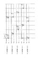
Hereinafter, the driving method of the present invention will be described. As shown in FIG. 1, the
ソース信号線18には寄生容量(図示せず)が存在する。寄生容量は、ソース信号線18とゲート信号線17とのクロス部の容量、トランジスタ11b、11cのチャンネル容量などにより発生する。
The
ソース信号線18の電流値変化に要する時間tは浮遊容量の大きさをC、ソース信号線の電圧をV、ソース信号線に流れる電流をIとするとt=C・V/Iであるため電流値を10倍大きくできることは電流値変化に要する時間が10分の1近くまで短くできる、またはソース信号線18の寄生容量が10倍になっても所定の電流値に変化できるということを示す。従って、短い水平走査期間内に所定の電流値を書きこむためには電流値を増加させることが有効である。
The time t required to change the current value of the
入力電流を10倍にすると出力電流も10倍となり、ELの輝度が10倍となるため所定の輝度を得るために、図1のトランジスタ11dの導通期間を従来の10分の1とし、発光期間を10分の1とすることで、所定輝度を表示するようにした。なお、10倍を例示して説明しているのは理解を容易にするためである。10倍に限定するものでないことは言うまでもない。
When the input current is increased by 10 times, the output current is also increased by 10 times, and the EL brightness is increased by 10 times. Therefore, in order to obtain a predetermined brightness, the conduction period of the
つまり、ソース信号線18の寄生容量の充放電を十分に行い、所定の電流値を画素16のトランジスタ11aにプログラムするためには、ソースドライバ回路14から比較的大きな電流を出力する必要がある。しかし、このように大きな電流をソース信号線18に流すとこの電流値が画素にプログラムされてしまい、所定の電流に対し大きな電流がEL素子15に流れる。たとえば、10倍の電流でプログラムすれば、当然、10倍の電流がEL素子15に流れ、EL素子15は10倍の輝度で発光する。所定の発光輝度にするためには、EL素子15に流れる時間を1/10にすればよい。このように駆動することにより、ソース信号線18の寄生容量を十分に充放電できるし、所定の発光輝度を得ることができる。
That is, in order to sufficiently charge and discharge the parasitic capacitance of the
なお、10倍の電流値を画素のトランジスタ11a(正確にはコンデンサ19の端子電圧を設定している)に書き込み、EL素子15のオン時間を1/10にするとしたがこれは一例である。場合によっては、10倍の電流値を画素のトランジスタ11aに書き込み、EL素子15のオン時間を1/5にしてもよい。逆に10倍の電流値を画素のトランジスタ11aに書き込み、EL素子15のオン時間を1/2倍にする場合もあるであろう。
It should be noted that although 10 times the current value is written in the
本発明は、画素への書き込み電流を所定値以外の値にし、EL素子15に流れる電流を間欠状態にして駆動することに特徴がある。本明細書では説明を容易にするため、N倍の電流値を画素のトランジスタ11に書き込み、EL素子15のオン時間を1/N倍にするとして説明する。しかし、これに限定するものではなく、N1倍の電流値を画素のトランジスタ11に書き込み、EL素子15のオン時間を1/(N2)倍(N1とN2とは異なる)でもよいことは言うまでもない。
The present invention is characterized in that the pixel write current is set to a value other than a predetermined value and the current flowing through the
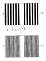
白ラスター表示において、表示画面50の1フィールド(フレーム)期間の平均輝度をB0と仮定する。この時、各画素16の輝度B1が平均輝度B0よりも高くなるように電流(電圧)プログラムを行う駆動方法である。かつ、少なくとも1フィールド(フレーム)期間において、非表示領域52が発生するようにする駆動方法である。したがって、本発明の駆動方法では、1フィールド(フレーム)期間の平均輝度はB1よりも低くなる。
In the white raster display, it is assumed that the average luminance in one field (frame) period of the
なお、間欠する間隔(非表示領域52/非表示領域53)は等間隔に限定するものではない。たとえば、ランダムでもよい(全体として、表示期間もしくは非表示期間が所定値(一定割合)となればよい)。また、RGBで異なっていてもよい。つまり、白(ホワイト)バランスが最適になるように、R、G、B表示期間もしくは非表示期間が所定値(一定割合)となるように調整(設定)すればよい。
The intermittent intervals (
本発明の駆動方法の説明を容易にするため、1/Nとは、1F(1フィールドまたは1フレーム)を基準にしてこの1Fを1/Nにするとして説明する。しかし、1画素行が選択され、電流値がプログラムされる時間(通常、1水平走査期間(1H))があるし、また、走査状態によっては誤差も生じることは言うまでもない。 In order to facilitate the description of the driving method of the present invention, 1 / N is described on the assumption that 1F is set to 1 / N on the basis of 1F (one field or one frame). However, there is a time during which one pixel row is selected and the current value is programmed (usually, one horizontal scanning period (1H)), and it goes without saying that an error may occur depending on the scanning state.
たとえば、N=10倍の電流で画素16に電流プログラムし、1/5の期間の間、EL素子15を点灯させてもよい。EL素子15は、10/5=2倍の輝度で点灯する。N=2倍の電流で画素16に電流プログラムし、1/4の期間の間、EL素子15を点灯させてもよい。EL素子15は、2/4=0.5倍の輝度で点灯する。つまり、本発明は、N=1倍でない電流でプログラムし、かつ、常時点灯(1/1、つまり、間欠表示でない)状態以外の表示を実施するものである。また、EL素子15に供給する電流を1フレーム(あるいは1フィールド)の期間において、少なくとも1回、オフする駆動方式である。また、所定値よりも大きな電流で画素16にプログラムし、少なくとも、間欠表示を実施する駆動方式である。
For example, the
有機(無機)EL表示装置は、CRTのように電子銃で線表示の集合として画像を表示するディスプレイとは表示方法が基本的に異なる点にも課題がある。つまり、EL表示装置では、1F(1フィールドあるいは1フレーム)の期間の間は、画素に書き込んだ電流(電圧)を保持する。そのため、動画表示を行うと表示画像の輪郭ぼけが発生するという課題が発生する。 The organic (inorganic) EL display device also has a problem in that the display method is basically different from a display that displays an image as a set of line displays with an electron gun, such as a CRT. That is, in the EL display device, the current (voltage) written to the pixel is held for a period of 1F (1 field or 1 frame). For this reason, when a moving image is displayed, there is a problem that the outline of the display image is blurred.
本発明では、1F/Nの期間の間だけ、EL素子15に電流を流し、他の期間(1F(N−1)/N)は電流を流さない。この駆動方式を実施し画面の一点を観測した場合を考える。この表示状態では1Fごとに画像データ表示、黒表示(非点灯)が繰り返し表示される。つまり、画像データ表示状態が時間的に間欠表示状態となる。動画データ表示を、間欠表示状態でみると画像の輪郭ぼけがなくなり良好な表示状態を実現できる。つまり、CRTに近い動画表示を実現することができる。
In the present invention, current is passed through the
本発明の駆動方法では、間欠表示を実現する。しかし、間欠表示は、トランジスタ11dを1H周期でオンオフ制御するだけでよい。したがって、回路のメインクロックは従来と変わらないため、回路の消費電力が増加することもない。液晶表示パネルでは、間欠表示を実現するために画像メモリが必要である。本発明は、画像データは各画素16に保持されている。したがって、間欠表示を実施するための画像メモリは不要である。
In the driving method of the present invention, intermittent display is realized. However, the intermittent display only needs to be turned on / off for the
本発明はスイッチングのトランジスタ11d、あるいはトランジスタ11eなどをオンオフさせるだけでEL素子15に流す電流を制御する。つまり、EL素子15に流れる電流Iwをオフしても、画像データはそのままコンデンサ19の保持されている。したがって、次のタイミングでトランジスタ11dなどをオンさせ、EL素子15に電流を流せば、その流れる電流は前に流れていた電流値と同一である。本発明では黒挿入(黒表示などの間欠表示)を実現する際においても、回路のメインクロックをあげる必要がない。また、時間軸伸張を実施する必要もないための画像メモリも不要である。また、有機EL素子15は電流を印加してから発光するまでの時間が短く、高速に応答する。そのため、動画表示に適し、さらに間欠表示を実施することにより従来のデータ保持型の表示パネル(液晶表示パネル、EL表示パネルなど)の問題である動画表示の問題を解決できる。
In the present invention, the current supplied to the
さらに、大型の表示装置でソース信号線18の配線長が長くなり、ソース信号線18の寄生容量が大きくなる場合は、N値を大きくすることにより対応できる。ソース信号線18に印加するプログラム電流値をN倍にした場合、ゲート信号線17b(トランジスタ11d)の導通期間を1F/Nとすればよい。これによりテレビ、モニターなどの大型表示装置などにも適用が可能である。
Further, in the case where the wiring length of the
以下、図面を参照しながら、本発明の駆動方法についてさらに詳しく説明をする。ソース信号線18の寄生容量は、隣接したソース信号線18間の結合容量、ソースドライブIC(回路)14のバッファ出力容量、ゲート信号線17とソース信号線18とのクロス容量などにより発生する。この寄生容量は通常10pF以上となる。電圧駆動の場合は、ソースドライバIC14からは低インピーダンスで電圧がソース信号線18に印加されるため、寄生容量が多少大きくとも駆動では問題とならない。
Hereinafter, the driving method of the present invention will be described in more detail with reference to the drawings. The parasitic capacitance of the
しかし、電流駆動では特に黒レベルの画像表示では20nA以下の微小電流で画素のコンデンサ19をプログラムする必要がある。したがって、寄生容量が所定値以上の大きさで発生すると、1画素行にプログラムする時間(通常、1H以内、ただし、2画素行を同時に書き込む場合もあるので1H以内に限定されるものではない。)内に寄生容量を充放電することができない。1H期間で充放電できなれば、画素への書き込み不足となり、解像度がでない。
However, current driving requires that the
図1の画素構成の場合、図3の(a)に示すように、電流プログラム時は、プログラム電流Iwがソース信号線18に流れる。この電流Iwがトランジスタ11aを流れ、Iwを流す電流が保持されるように、コンデンサ19に電圧設定(プログラム)される。このとき、トランジスタ11dはオープン状態(オフ状態)である。
In the case of the pixel configuration of FIG. 1, as shown in FIG. 3A, the program current Iw flows through the
次に、EL素子15に電流を流す期間は図3の(b)のように、トランジスタ11c、11bがオフし、トランジスタ11dが動作する。つまり、ゲート信号線17aにオフ電圧(Vgh)が印加され、トランジスタ11b、11cがオフする。一方、ゲート信号線17bにオン電圧(Vgl)が印加され、トランジスタ11dがオンする。
Next, during a period in which a current flows through the
今、電流I1が本来流す電流(所定値)のN倍であるとすると、図3の(b)のEL素子15に流れる電流もIwとなる。したがって、所定値の10倍の輝度でEL素子15は発光する。つまり、図12に図示するように、倍率Nを高くするほど、画素16の表示輝度Bも高くなる。したがって、倍率と画素16の輝度とは比例関係となる。
Assuming that the current I1 is N times the current (predetermined value) that flows originally, the current that flows in the
そこで、トランジスタ11dを本来オンする時間(約1F)の1/Nの期間だけオンさせ、他の期間(N−1)/N期間はオフさせれば、1F全体の平均輝度は所定の輝度となる。この表示状態は、CRTが電子銃で画面を走査しているのと近似する。異なる点は、画面全体の1/N(全画面を1とする)が点灯している点である(CRTでは、点灯している範囲は1画素行(厳密には1画素である)。
Therefore, if the
本発明では、この1F/Nの画像表示領域53が図13の(b)に示すように画面50の上から下に移動する。本発明では、1F/Nの期間の間だけ、EL素子15に電流が流れ、他の期間(1F・(N−1)/N)は電流が流れない。したがって、各画素16は間欠表示となる。しかし、人間の目には残像により画像が保持された状態となるので、全画面が均一に表示されているように見える。
In the present invention, the 1F / N
なお、図13に図示するように、書き込み画素行51aは非点灯表示52aとする。しかし、これは、図1、図2などの画素構成の場合である。図38などで図示するカレントミラーの画素構成では、書き込み画素行51aは点灯状態としてもよい。しかし、本明細書では、説明を容易にするため、主として、図1の画素構成を例示して説明をする。また、図13、図16などの所定駆動電流Iwよりも大きい電流でプログラムし、間欠駆動する駆動方法をN倍パルス駆動と呼ぶ。
As shown in FIG. 13, the
この表示状態では1Fごとに画像データ表示、黒表示(非点灯)が繰り返し表示される。つまり、画像データ表示状態が時間的に飛び飛び表示(間欠表示)状態となる。液晶表示パネル(本発明以外のEL表示パネル)では、1Fの期間、画素にデータが保持されているため、動画表示の場合は画像データが変化してもその変化に追従することができず、動画ボケとなっていた(画像の輪郭ボケ)。しかし、本発明では画像を間欠表示するため、画像の輪郭ぼけがなくなり良好な表示状態を実現できる。つまり、CRTに近い動画表示を実現することができる。 In this display state, image data display and black display (non-lighting) are repeatedly displayed every 1F. That is, the image data display state is a temporal display (intermittent display) state. In a liquid crystal display panel (an EL display panel other than the present invention), since data is held in pixels for a period of 1F, even if image data changes in the case of moving image display, the change cannot be followed. The video was blurred (outline blur in the image). However, since the image is intermittently displayed in the present invention, the outline of the image is not blurred and a good display state can be realized. That is, a moving image display close to a CRT can be realized.
なお、図13に図示するように、駆動するためには、画素16の電流プログラム期間(図1の画素構成においては、ゲート信号線17aのオン電圧Vglが印加されている期間)と、EL素子15をオフまたはオン制御している期間(図1の画素構成においては、ゲート信号線17bのオン電圧Vglまたはオフ電圧Vghが印加されている期間)とを独立に制御できる必要がある。したがって、ゲート信号線17aとゲート信号線17bは分離されている必要がある。
As shown in FIG. 13, in order to drive, the current program period of the pixel 16 (in the pixel configuration of FIG. 1, the period during which the ON voltage Vgl of the
たとえば、ゲートドライバ回路12から画素16に配線されたゲート信号線17が1本である場合、ゲート信号線17に印加されたロジック(VghまたはVgl)をトランジスタ11bに印加し、ゲート信号線17に印加されたロジックをインバータで変換して(VglまたはVgh)して、トランジスタ11dに印加するという構成では、本発明の駆動方法は実施できない。したがって、本発明では、ゲート信号線17aを操作するゲートドライバ回路12aと、ゲート信号線17bを操作するゲートドライバ回路12bが必要となる。
For example, when there is one
また、本発明の駆動方法は、図1の画素構成においても、電流プログラム期間(1H)以外の期間においても、非点灯表示にする駆動方法である。 In addition, the driving method of the present invention is a driving method for non-lighting display in the pixel configuration of FIG. 1 and in a period other than the current program period (1H).
図13の駆動方法のタイミングチャートを図14に図示する。なお、本発明などにおいて、特に断りがない時の画素構成は図1であるとする。図14でわかるように、各選択された画素行(選択期間は、1Hとしている)において、ゲート信号線17aにオン電圧(Vgl)が印加されている時(図14の(a)を参照)には、ゲート信号線17bにはオフ電圧(Vgh)が印加されている(図14の(b)を参照)。また、この期間は、EL素子15には電流が流れていない(非点灯状態)。選択されていない画素行において、ゲート信号線17aにオフ電圧(Vgh)が印加され、ゲート信号線17bにはオン電圧(Vgl)が印加されている。また、この期間は、EL素子15に電流が流れている(点灯状態)。また、点灯状態では、EL素子15は所定のN倍の輝度(N・B)で点灯し、その点灯期間は1F/Nである。したがって、1Fを平均した表示パネルの表示輝度は、(N・B)×(1/N)=B(所定輝度)となる。
FIG. 14 shows a timing chart of the driving method of FIG. In the present invention and the like, the pixel configuration when there is no particular notice is assumed to be FIG. As can be seen from FIG. 14, when the ON voltage (Vgl) is applied to the
図15は、図14の動作を各画素行に適用した実施例である。ゲート信号線17に印加する電圧波形を示している。電圧波形はオフ電圧をVgh(Hレベル)とし、オン電圧をVgl(Lレベル)としている。(1)(2)などの添え字は選択している画素行番号を示している。
FIG. 15 shows an embodiment in which the operation of FIG. 14 is applied to each pixel row. A voltage waveform applied to the
図15において、ゲート信号線17a(1)が選択され(Vgl電圧)、選択された画素行のトランジスタ11aからソースドライバ回路14に向かってソース信号線18にプログラム電流が流れる。このプログラム電流は所定値のN倍(説明を容易にするため、N=10として説明する。もちろん、所定値とは画像を表示するデータ電流であるから、白ラスター表示などでない限り固定値ではない。)である。したがって、コンデンサ19には10倍に電流がトランジスタ11aに流れるようにプログラムされる。画素行(1)が選択されている時は、図1の画素構成ではゲート信号線17b(1)はオフ電圧(Vgh)が印加され、EL素子15には電流が流れない。
In FIG. 15, the
1H後には、ゲート信号線17a(2)が選択され(Vgl電圧)、選択された画素行のトランジスタ11aからソースドライバ回路14に向かってソース信号線18にプログラム電流が流れる。このプログラム電流は所定値のN倍(説明を容易にするため、N=10として説明する)である。したがって、コンデンサ19には10倍に電流がトランジスタ11aに流れるようにプログラムされる。画素行(2)が選択されている時は、図1の画素構成ではゲート信号線17b(2)はオフ電圧(Vgh)が印加され、EL素子15には電流が流れない。しかし、先の画素行(1)のゲート信号線17a(1)にはオフ電圧(Vgh)が印加され、ゲート信号線17b(1)にはオン電圧(Vgl)が印加されるため、点灯状態となっている。
After 1H, the
次の1H後には、ゲート信号線17a(3)が選択され、ゲート信号線17b(3)はオフ電圧(Vgh)が印加され、画素行(3)のEL素子15には電流が流れない。しかし、先の画素行(1)(2)のゲート信号線17a(1)(2)にはオフ電圧(Vgh)が印加され、ゲート信号線17b(1)(2)にはオン電圧(Vgl)が印加されるため、点灯状態となっている。
After the next 1H, the
以上の動作を1Hの同期信号に同期して画像を表示していく。しかし、図15の駆動方式では、EL素子15には10倍の電流が流れる。したがって、表示画面50は約10倍の輝度で表示される。もちろん、この状態で所定の輝度表示を行うためには、プログラム電流を1/10にしておけばよいことは言うまでもない。しかし、1/10の電流であれば寄生容量などにより書き込み不足が発生するため、高い電流でプログラムし、非点灯領域52の挿入により所定の輝度を得るのは本発明の基本的な主旨である。
The above operation is displayed in synchronization with the 1H synchronization signal. However, in the driving method of FIG. 15, 10 times of current flows through the
なお、本発明の駆動方法において、所定電流よりも高い電流がEL素子15に流れるようにし、ソース信号線18の寄生容量を十分に充放電するという概念である。つまり、EL素子15にN倍の電流を流さなくともよい。たとえば、EL素子15に並列に電流経路を形成し(ダミーのEL素子を形成し、このEL素子は遮光膜を形成して発光させないなど)、ダミーEL素子とEL素子15に分流して電流を流しても良い。たとえば、信号電流が0.2μAのとき、プログラム電流を2.2μAとして、トランジスタ11aには2.2μAを流す。この電流のうち、信号電流0.2μAをEL素子15に流して、2μAをダミーのEL素子に流すなどの方式が例示される。つまり、図27のダミー画素行271を常時選択状態にする。なお、ダミー画素行は発光させないか、もしくは、遮光膜などを形成し、発光していても視覚的に見えないように構成する。
In the driving method of the present invention, the concept is that a current higher than a predetermined current flows in the
以上のように構成することにより、ソース信号線18に流す電流をN倍に増加させることにより、駆動用トランジスタ11aにN倍の電流が流れるようにプログラムすることができ、かつ、電流EL素子15には、N倍よりは十分小さい電流を流すことができることになる。以上の方法では、図5に図示するように、非点灯領域52を設けることなく、全表示画面50を画像表示領域53とすることができる。
With the above configuration, by increasing the current flowing through the
図13の(a)は表示画面50への書き込み状態を図示している。図13の(a)において、51aは書き込み画素行である。ソースドライバIC14から各ソース信号線18にプログラム電流が供給される。なお、図13などでは1H期間に書き込む画素行は1行である。しかし、何ら1Hに限定するものではなく、0.5H期間でも、2H期間でもよい。また、ソース信号線18にプログラム電流を書き込むとしたが、本発明は電流プログラム方式に限定するものではなく、ソース信号線18に書き込まれるのは電圧である電圧プログラム方式(図46など)でもよい。
FIG. 13A shows a state of writing on the
図13の(a)において、ゲート信号線17aが選択されるとソース信号線18に流れる電流がトランジスタ11aにプログラムされる。この時、ゲート信号線17bはオフ電圧が印加されEL素子15には電流が流れない。これは、EL素子15側にトランジスタ11dがオン状態であると、ソース信号線18からEL素子15の容量成分が見え、この容量に影響されてコンデンサ19に十分に正確な電流プログラムができなくなるためである。したがって、図1の構成を例にすれば、図13の(b)で示すように電流を書き込まれている画素行は非点灯領域52となる。
In FIG. 13A, when the
今、N(ここでは、先に述べたようにN=10とする)倍の電流でプログラムしたとすれば、画面の輝度は10倍になる。したがって、表示画面50の90%の範囲を非点灯領域52とすればよい。したがって、画像表示領域の水平走査線がQCIFの220本(S=220)とすれば、22本と表示領域53とし、220−22=198本を非表示領域52とすればよい。一般的に述べれば、水平走査線(画素行数)をSとすれば、S/Nの領域を表示領域53とし、この表示領域53をN倍の輝度で発光させる。そして、この表示領域53を画面の上下方向に走査する。したがって、S(N−1)/Nの領域は非点灯領域52とする。この非点灯領域は黒表示(非発光)である。また、この非発光部52はトランジスタ11dをオフさせることにより実現する。なお、N倍の輝度で点灯させるとしたが、当然のことながら明るさ調整、ガンマ調整によりN倍の値を調整することは言うまでもない。
Now, if the current is programmed with N times (N = 10 as described above), the screen brightness will be 10 times. Therefore, a 90% range of the
また、先の実施例で、10倍の電流でプログラムしたとすれば、画面の輝度は10倍になり、表示画面50の90%の範囲を非点灯領域52とすればよいとした。しかし、これは、RGBの画素を共通に非点灯領域52とすることに限定するものではない。例えば、Rの画素は、1/8を非点灯領域52とし、Gの画素は、1/6を非点灯領域52とし、Bの画素は、1/10を非点灯領域52と、それぞれの色により変化させてもよい。また、RGBの色で個別に非点灯領域52(あるいは点灯領域53)を調整できるようにしてもよい。これらを実現するためには、R、G、Bで個別のゲート信号線17bが必要になる。しかし、以上のRGBの個別調整を可能にすることにより、ホワイトバランスを調整することが可能になり、各階調において色のバランス調整が容易になる(図41を参照のこと)。
Further, in the previous embodiment, if programming was performed with 10 times the current, the brightness of the screen would be 10 times, and the 90% range of the
図13の(b)に図示するように、書き込み画素行51aを含む画素行が非点灯領域52とし、書き込み画素行51aよりも上画面のS/N(時間的には1F/N)の範囲を表示領域53とする(書き込み走査が画面の上から下方向の場合、画面を下から上に走査する場合は、その逆となる)。画像表示状態は、表示領域53が帯状になって、画面の上から下に移動する。
As shown in FIG. 13B, the pixel row including the
図13の表示では、1つの表示領域53が画面の上から下方向に移動する。フレームレートが低いと、表示領域53が移動するのが視覚的に認識される。特に、まぶたを閉じた時、あるいは顔を上下に移動させた時などに認識されやすくなる。
In the display of FIG. 13, one
この課題に対しては、図16に図示するように、表示領域53を複数に分割するとよい。この分割された総和がS(N−1)/Nの面積となれば、図13の明るさと同等になる。なお、分割された表示領域53は等しく(等分に)する必要はない。また、分割された非表示領域52も等しくする必要はない。
For this problem, the
以上のように、表示領域53を複数に分割することにより画面のちらつきは減少する。したがって、フリッカの発生はなく、良好な画像表示を実現できる。なお、分割はもっと細かくしてもよい。しかし、分割するほど動画表示性能は低下する。
As described above, screen flickering is reduced by dividing
図17はゲート信号線17の電圧波形およびELの発光輝度を図示している。図17で明らかなように、ゲート信号線17bをVglにする期間(1F/N)を複数に分割(分割数K)している。つまり、Vglにする期間は1F/(K・N)の期間をK回実施する。このように制御すれば、フリッカの発生を抑制でき、低フレームレートの画像表示を実現できる。また、この画像の分割数も可変できるように構成することが好ましい。たとえば、ユーザーが明るさ調整スイッチを押すことにより、あるいは明るさ調整ボリウムを回すことにより、この変化を検出してKの値を変更してもよい。また、ユーザーが輝度を調整するように構成してもよい。表示する画像の内容、データにより手動で、あるいは自動的に変化させるように構成してもよい。
FIG. 17 shows the voltage waveform of the
なお、図17などにおいて、ゲート信号線17bをVglにする期間(1F/N)を複数に分割(分割数K)し、Vglにする期間は1F/(K・N)の期間をK回実施するとしたがこれに限定するものではない。1F/(K・N)の期間をL(L≠K)回実施してもよい。つまり、本発明は、EL素子15に流す期間(時間)を制御することにより表示画面50を表示するものである。したがって、1F/(K・N)の期間をL(L≠K)回実施することは本発明の技術的思想に含まれる。また、Lの値を変化させることにより、表示画像50の輝度をデジタル的に変更することができる。たとえば、L=2とL=3では50%の輝度(コントラスト)変化となる。また、画像の表示領域53を分割する時、ゲート信号線17bをVglにする期間は同一期間に限定するものではない。
In FIG. 17 and the like, the period (1F / N) for setting the
以上の実施例は、EL素子15に流れる電流を遮断し、また、EL素子に流れる電流を接続することにより、表示画面50をオンオフ(点灯、非点灯)するものであった。つまり、コンデンサ19に保持された電荷によりトランジスタ11aに複数回、略同一電流を流すものである。本発明はこれに限定するものではない。たとえば、コンデンサ19に保持された電荷を充放電させることにより、表示画面50をオンオフ(点灯、非点灯)する方式でもよい。
In the above embodiment, the current flowing through the
図18は図16の画像表示状態を実現するための、ゲート信号線17に印加する電圧波形である。図18と図15の差異は、ゲート信号線17bの動作である。ゲート信号線17bは画面を分割する個数に対応して、その個数分だけオンオフ(VglとVgh)動作する。他の点は図15と同一であるので説明を省略する。
FIG. 18 shows voltage waveforms applied to the
EL表示装置では黒表示は完全に非点灯であるから、液晶表示パネルを間欠表示した場合のように、コントラスト低下もない。また、図1、図2、図32、図43、図117の構成においては、トランジスタ11dをオンオフ操作するだけで間欠表示を実現できる。また、図38、図51、図115の構成においては、トランジスタ素子11eをオンオフ操作するだけで、間欠表示を実現することができる。また、図113においては切り替え回路1131を制御することにより間欠表示を実現できる。また、図114においては、トランジスタ11gをオンオフ制御することにより間欠表示を実現できる。これは、コンデンサ19に画像データがメモリ(アナログ値であるから階調数は無限大)されているからである。つまり、各画素16に、画像データは1Fの期間中は保持されている。この保持されている画像データに相当する電流をEL素子15に流すか否かをトランジスタ11d、11eの制御により実現しているのである。
In the EL display device, since the black display is completely unlit, there is no reduction in contrast as in the case where the liquid crystal display panel is intermittently displayed. In the configurations of FIGS. 1, 2, 32, 43, and 117, intermittent display can be realized only by turning on and off the
したがって、以上の駆動方法は、電流駆動方式に限定されるものではなく、電圧駆動方式にも適用できるものである。つまり、EL素子15に流す電流が各画素内で保存している構成において、駆動用トランジスタ11をEL素子15間の電流経路をオンオフすることにより、間欠駆動を実現するものである。
Therefore, the above driving method is not limited to the current driving method, but can also be applied to the voltage driving method. That is, in the configuration in which the current flowing through the
コンデンサ19の端子電圧を維持することはフリッカ低減と低消費電力化に重要である。1フィールド(フレーム)期間でコンデンサ19の端子電圧が変化(充放電)すると、画面輝度が変化する。画面輝度が変化すると、フレームレートが低下した時にちらつき(フリッカなど)が発生するからである。トランジスタ11aが1フレーム(1フィールド)期間でEL素子15に流す電流は、少なくとも65%以下に低下しないようにする必要がある。この65%とは、画素16に書き込み、EL素子15に流す電流の最初が100%とした時、次のフレーム(フィールド)で前記画素16に書き込む直前のEL素子15に流す電流が65%以上とすることである。
Maintaining the terminal voltage of the
図1の画素構成では、間欠表示を実現する場合としない場合では、1画素を構成するトランジスタ11の個数に変化はない。つまり、画素構成はそのままで、ソース信号線18の寄生容量の影響と除去し、良好な電流プログラムを実現している。その上、CRTに近い動画表示を実現しているのである。
In the pixel configuration of FIG. 1, there is no change in the number of
また、ゲートドライバ回路12の動作クロックはソースドライバ回路14の動作クロックに比較して十分に遅いため、回路のメインクロックが高くなるということはない。また、Nの値の変更も容易である。
Further, since the operation clock of the
なお、画像表示方向(画像書き込み方向)は、1フィールド(1フレーム)目では画面の上から下方向とし、つぎの第2フィールド(フレーム)目では画面の下から上方向としてもよい。つまり、上から下方向と、下から上方向とを交互にくりかえす。 The image display direction (image writing direction) may be from the top to the bottom in the first field (one frame) and from the bottom to the top in the second field (frame). In other words, the top-to-bottom direction and the bottom-to-top direction are alternately repeated.
さらに、1フィールド(1フレーム)目では画面の上から下方向とし、いったん、全画面を黒表示(非表示)とした後、つぎの第2フィールド(フレーム)目では画面の下から上方向としてもよい。また、いったん、全画面を黒表示(非表示)としてもよい。 In the first field (one frame), the screen is displayed from the top to the bottom. Once the entire screen is displayed in black (not displayed), the second field (frame) is displayed from the bottom to the top. Also good. Alternatively, the entire screen may be displayed black (not displayed) once.
なお、以上の駆動方法の説明では、画面の書き込み方法を画面の上から下あるいは下から上としたが、これに限定するものではない。画面の書き込み方向は絶えず、画面の上から下あるいは下から上と固定し、非表示領域52の動作方向を1フィールド目では画面の上から下方向とし、つぎの第2フィールド目では画面の下から上方向としてもよい。また、1フレームを3フィールドに分割し、第1のフィールドではR、第2のフィールドではG、第3のフィールドではBとして、3フィールドで1フレームを形成するとしてもよい。また、1水平走査期間(1H)ごとに、R、G、Bを切り替えて表示してもよい(図125から図132とその説明などを参照のこと)。以上の事項は他の本発明の実施例でも同様である。
In the above description of the driving method, the screen writing method is set from the top to the bottom or from the bottom to the top, but the present invention is not limited to this. The screen writing direction is constantly fixed from top to bottom or from bottom to top, and the
非表示領域52は完全に非点灯状態である必要はない。微弱な発光あるいは低輝度の画像表示があっても実用上は問題ない。つまり、画像表示領域53よりも表示輝度が低い領域と解釈するべきである。また、非表示領域52とは、R、G、B画像表示のうち、1色または2色のみが非表示状態という場合も含まれる。また、R、G、B画像表示のうち、1色または2色のみが低輝度の画像表示状態という場合も含まれる。
The
基本的には表示領域53の輝度(明るさ)が所定値に維持される場合、表示領域53の面積が広くなるほど、画面50の輝度は高くなる。たとえば、表示領域53の輝度が100(nt)の場合、表示領域53が全画面50に占める割合が10%から20%にすれば、画面の輝度は2倍となる。したがって、全画面50に占める表示領域53の面積を変化させることにより、画面の表示輝度を変化することができる。画面50の表示輝度は画面50に占める表示領域53の割合に比例する。
Basically, when the brightness (brightness) of the
表示領域53の面積はシフトレジスタ回路61へのデータパルス(ST2)を制御することにより、任意に設定できる。また、データパルスの入力タイミング、周期を変化させることにより、図16の表示状態と図13の表示状態とを切り替えることができる。1F周期でのデータパルス数を多くすれば、画面50は明るくなり、少なくすれば、画面50は暗くなる。また、連続してデータパルスを印加すれば図13の表示状態となり、間欠にデータパルスを入力すれば図16の表示状態となる。
The area of the
図19の(a)は図13のように表示領域53が連続している場合の明るさ調整方式である。図19(a1)の画面50の表示輝度が最も明るい。図19(a2)の画面50の表示輝度が次に明るく、図19(a3)の画面50の表示輝度が最も暗い。図19の(a)は最も動画表示に適する。
FIG. 19A shows a brightness adjustment method when the
図19(a1)から図19(a3)への変化(あるいはその逆)は、先にも記載したようにゲートドライバ回路12のシフトレジスタ回路61などの制御により、容易に実現できる。この際、図1のVdd電圧は変化させる必要がない。つまり、電源電圧を変化させずに表示画面50の輝度変化を実施できる。また、図19(a1)から図19(a3)への変化の際、画面のガンマ特性は全く変化しない。したがって、画面50の輝度によらず、表示画像のコントラスト、階調特性が維持される。これは本発明の効果のある特徴である。
The change from FIG. 19 (a1) to FIG. 19 (a3) (or vice versa) can be easily realized by controlling the shift register circuit 61 of the
従来の画面の輝度調整では、画面50の輝度が低い時は、階調性能が低下する。つまり、高輝度表示の時は64階調表示を実現できても、低輝度表示の時は、半分以下の階調数しか表示できない場合がほとんどである。これに比較して、本発明の駆動方法では、画面の表示輝度に依存せず、最高の64階調表示を実現できる。
In the conventional screen brightness adjustment, when the brightness of the
図19の(b)は図16のように表示領域53が分散している場合の明るさ調整方式である。図19(b1)の画面50の表示輝度が最も明るい。図19(b2)の画面50の表示輝度が次に明るく、図19(b3)の画面50の表示輝度が最も暗い。図19(b1)から図19(b3)への変化(あるいはその逆)は、先にも記載したようにゲートドライバ回路12のシフトレジスタ回路61などの制御により、容易に実現できる。図19の(b)のように表示領域53を分散させれば、低フレームレートでもフリッカが発生しない。
FIG. 19B shows a brightness adjustment method when the
さらに低フレームレートでも、フリッカが発生しないようにするには、図19の(c)のように表示領域53を細かく分散させればよい。しかし、動画の表示性能は低下する。したがって、動画を表示するには、図19の(a)の駆動方法が適している。静止画を表示し、低消費電力化を要望する時は、図19の(c)の駆動方法が適している。図19の(a)から図19の(c)の駆動方法の切り替えも、シフトレジスタ61の制御により容易に実現できる。
In order to prevent flicker from occurring even at a lower frame rate, the
以上の実施例は、主として、N=2倍、4倍などにする実施例であった。しかし、本発明は整数倍に限定されるものではないことは言うまでもない。また、N=2以上に限定されるものでもない。たとえば、ある時刻で表示画面50の半分以下の領域を非点灯領域52とすることもある。所定値の5/4倍の電流Iwで電流プログラムし、1Fの4/5期間点灯させれば、所定の輝度を実現できる。
The above embodiments are mainly embodiments in which N = 2 times, 4 times, and the like. However, it goes without saying that the present invention is not limited to integer multiples. Moreover, it is not limited to N = 2 or more. For example, an area less than half of the
本発明はこれに限定されるものではない。一例として、10/4倍の電流Iwで電流プログラミングし、1Fの4/5期間の間点灯させるという方法もある。この場合は、所定輝度の2倍で点灯する。また、5/4倍の電流Iwで電流プログラミングし、1Fの2/5期間の間点灯させるという方法もある。この場合は、所定輝度の1/2倍で点灯する。また、5/4倍の電流Iwで電流プログラミングし、1Fの1/1期間の間点灯させるという方法もある。この場合は、所定輝度の5/4倍で点灯する。 The present invention is not limited to this. As an example, there is a method in which current programming is performed with a current Iw that is 10/4 times, and lighting is performed for a 4/5 period of 1F. In this case, it is lit at twice the predetermined luminance. There is also a method in which current programming is performed with a current Iw that is 5/4 times, and lighting is performed for a period of 2/5 of 1F. In this case, the light is lit at half the predetermined luminance. There is also a method in which current programming is performed with a current Iw that is 5/4 times, and lighting is performed for a 1/1 period of 1F. In this case, it is lit at 5/4 times the predetermined luminance.
つまり、本発明は、プログラム電流の大きさと、1Fの点灯期間を制御することにより、表示画面の輝度を制御する方式である。かつ、1F期間よりも短い期間点灯させることにより、非点灯領域52を挿入でき、動画表示性能を向上できる。1Fの期間、常時点灯させることにより明るい画面を表示できる。
That is, the present invention is a method for controlling the luminance of the display screen by controlling the magnitude of the program current and the lighting period of 1F. Further, by turning on the light for a period shorter than the 1F period, the
画素に書き込む電流(ソースドライバ回路14から出力するプログラム電流)は、画素サイズがA平方mmとし、白ラスター表示所定輝度をB(nt)とした時、プログラム電流I(μA)は、
(A×B)/20 ≦ I ≦ (A×B)
の範囲とすることが好ましい。発光効率が良好となり、かつ、電流書込み不足が解消する。
When the pixel size is A square mm and the white raster display predetermined luminance is B (nt), the current written into the pixel (program current output from the source driver circuit 14) is:
(A × B) / 20 ≦ I ≦ (A × B)
It is preferable to set it as the range. Luminous efficiency is improved and insufficient current writing is eliminated.
さらに、好ましくは、プログラム電流I(μA)は、
(A×B)/10 ≦ I ≦ (A×B)
の範囲とすることが好ましい。
Further preferably, the program current I (μA) is
(A × B) / 10 ≦ I ≦ (A × B)
It is preferable to set it as the range.
図20はソース信号線18に流れる電流を増大させる他の実施例の説明図である。基本的に複数の画素行を同時に選択し、複数の画素行をあわせた電流でソース信号線18の寄生容量などを充放電し電流書き込み不足を大幅に改善する方式である。ただし、複数の画素行を同時に選択するため、1画素あたりの駆動する電流を減少させることができる。したがって、EL素子15に流れる電流を減少させることができる。ここで、説明を容易にするため、一例として、N=10として説明する(ソース信号線18に流す電流を10倍にする)。
FIG. 20 is an explanatory diagram of another embodiment in which the current flowing through the
図20で説明する本発明は、画素行は同時にM画素行を選択する。ソースドライバIC14からは所定電流のN倍電流をソース信号線18に印加する。各画素にはEL素子15に流す電流のN/M倍の電流がプログラムされる。一例として、EL素子15を所定発光輝度とするために、EL素子15に流れる時間を1フレーム(1フィールド)のM/N時間にする(ただし、M/Nに限定するものではなない。M/Nとするのは理解を容易にするためである。先にも説明したように、表示する画面50輝度により自由に設定できることはいうまでもない。)。このように駆動することにより、ソース信号線18の寄生容量を十分に充放電でき、良好な解像度を所定の発光輝度を得ることができる。
The present invention described with reference to FIG. 20 selects M pixel rows at the same time as the pixel rows. From the
1フレーム(1フィールド)のM/Nの期間の間だけ、EL素子15に電流を流し、他の期間(1F(N−1)M/N)は電流を流さないように表示する。この表示状態では1Fごとに画像データ表示、黒表示(非点灯)が繰り返し表示される。つまり、画像データ表示状態が時間的に飛び飛び表示(間欠表示)状態となる。したがって、画像の輪郭ぼけがなくなり良好な動画表示を実現できる。また、ソース信号線18にはN倍の電流で駆動するため、寄生容量の影響をうけず、高精細表示パネルにも対応できる。
Display is performed so that current flows through the
図21は、図20の駆動方法を実現するための駆動波形の説明図である。信号波形はオフ電圧をVgh(Hレベル)とし、オン電圧をVgl(Lレベル)としている。各信号線の添え字は画素行の番号((1)(2)(3)など)を記載している。なお、行数はQCIF表示パネルの場合は220本であり、VGAパネルでは480本である。 FIG. 21 is an explanatory diagram of drive waveforms for realizing the drive method of FIG. The signal waveform has an off voltage of Vgh (H level) and an on voltage of Vgl (L level). The subscript of each signal line describes the number of the pixel row ((1) (2) (3) etc.). The number of rows is 220 for the QCIF display panel and 480 for the VGA panel.
図21において、ゲート信号線17a(1)が選択され(Vgl電圧)、選択された画素行のトランジスタ11aからソースドライバ回路14に向かってソース信号線18にプログラム電流が流れる。ここでは説明を容易にするため、まず、書き込み画素行51aが画素行(1)番目であるとして説明する。
In FIG. 21, the
また、ソース信号線18に流れるプログラム電流は所定値のN倍(説明を容易にするため、N=10として説明する。もちろん、所定値とは画像を表示するデータ電流であるから、白ラスター表示などでない限り固定値ではない。)である。また、5画素行が同時に選択(M=5)として説明をする。したがって、理想的には1つの画素のコンデンサ19には2倍(N/M=10/5=2)に電流がトランジスタ11aに流れるようにプログラムされる。
The program current flowing through the
書き込み画素行が(1)画素行目である時、図21で図示したように、ゲート信号線17aは(1)(2)(3)(4)(5)が選択されている。つまり、画素行(1)(2)(3)(4)(5)のスイッチング用トランジスタ11b、トランジスタ11cがオン状態である。また、ゲート信号線17bはゲート信号線17aの逆位相となっている。したがって、画素行(1)(2)(3)(4)(5)のスイッチング用トランジスタ11dがオフ状態であり、対応する画素行のEL素子15には電流が流れていない。つまり、非点灯状態52である。
When the writing pixel row is the (1) pixel row, as shown in FIG. 21, (1), (2), (3), (4), and (5) are selected for the
理想的には、5画素のトランジスタ11aが、それぞれIw×2の電流をソース信号線18に流す(つまり、ソース信号線18にはIw×2×N=Iw×2×5=Iw×10。したがって、本発明のN倍パルス駆動を実施しない場合が所定電流Iwとすると、Iwの10倍の電流がソース信号線18に流れる)。
Ideally, each of the five-
以上の動作(駆動方法)により、各画素16のコンデンサ19には、2倍の電流がプログラムされる。ここでは、理解を容易にするため、各トランジスタ11aは特性(Vt、S値)が一致しているとして説明をする。
With the above operation (driving method), a double current is programmed in the
同時に選択する画素行が5画素行(M=5)であるから、5つの駆動用トランジスタ11aが動作する。つまり、1画素あたり、10/5=2倍の電流がトランジスタ11aに流れる。ソース信号線18には、5つのトランジスタ11aのプログラム電流を加えた電流が流れる。たとえば、書き込み画素行51aに、本来、書き込む電流Iwとし、ソース信号線18には、Iw×10の電流を流す。書き込み画素行(1)より以降に画像データを書き込む書き込み画素行51bソース信号線18への電流量を増加させるため、補助的に用いる画素行である。しかし、書き込み画素行51bは後に正規の画像データが書き込まれるので問題がない。
Since five pixel rows (M = 5) are selected at the same time, the five
したがって、4画素行51bにおいて、1H期間の間は51aと同一表示である。そのため、書き込み画素行51aと電流を増加させるために選択した画素行51bとを少なくとも非表示状態52とするのである。ただし、図38のようなカレントミラーの画素構成、その他の電圧プログラム方式の画素構成では表示状態としてもよい。
Accordingly, the same display as 51a is performed in the four
1H後には、ゲート信号線17a(1)は非選択となり、ゲート信号線17bにはオン電圧(Vgl)が印加される。また、同時に、ゲート信号線17a(6)が選択され(Vgl電圧)、選択された画素行(6)のトランジスタ11aからソースドライバ回路14に向かってソース信号線18にプログラム電流が流れる。このように動作することにより、画素行(1)には正規の画像データが保持される。
After 1H, the
次の、1H後には、ゲート信号線17a(2)は非選択となり、ゲート信号線17bにはオン電圧(Vgl)が印加される。また、同時に、ゲート信号線17a(7)が選択され(Vgl電圧)、選択された画素行(7)のトランジスタ11aからソースドライバ回路14に向かってソース信号線18にプログラム電流が流れる。このように動作することにより、画素行(2)には正規の画像データが保持される。以上の動作と1画素行ずつシフトしながら走査することにより1画面が書き換えられる。
After the next 1H, the
図20の駆動方法では、各画素には2倍の電流(電圧)でプログラムを行うため、各画素のEL素子15の発光輝度は理想的には2倍となる。したがって、表示画面の輝度は所定値よりも2倍となる。これを所定の輝度とするためには、図16に図示するように、書き込み画素行51を含み、かつ表示画面50の1/2の範囲を非表示領域52とすればよい。
In the driving method of FIG. 20, since each pixel is programmed with twice the current (voltage), the light emission luminance of the
図13と同様に、図20のように1つの表示領域53が画面の上から下方向に移動すると、フレームレートが低いと、表示領域53が移動するのが視覚的に認識される。特に、まぶたを閉じた時、あるいは顔を上下に移動させた時などに認識されやすくなる。
As in FIG. 13, when one
この課題に対しては、図22に図示するように、表示領域53を複数に分割するとよい。分割された非表示領域52を加えた部分がS(N−1)/Nの面積となれば、分割しない場合と同一となる。
For this problem, the
図23はゲート信号線17に印加する電圧波形である。図21と図23との差異は、基本的にはゲート信号線17bの動作である。ゲート信号線17bは画面を分割する個数に対応して、その個数分だけオンオフ(VglとVgh)動作する。他の点は図21とほぼ同一あるいは類推できるので説明を省略する。
FIG. 23 shows voltage waveforms applied to the
以上のように、表示領域53を複数に分割することにより画面のちらつきは減少する。したがって、フリッカの発生はなく、良好な画像表示を実現できる。なお、分割はもっと細かくしてもよい。しかし、分割すればするほどフリッカは軽減する。特にEL素子15の応答性は速いため、5μsecよりも小さい時間でオンオフしても、表示輝度の低下はない。
As described above, screen flickering is reduced by dividing
本発明の駆動方法において、EL素子15のオンオフは、ゲート信号線17bに印加する信号のオンオフで制御できる。そのため、本発明の駆動方法では、KHzオーダーの低周波数で制御が可能である。また、黒画面挿入(非表示領域52挿入)を実現するのには、画像メモリなどを必要としない。したがって、低コストで本発明の駆動回路あるいは方法を実現できる。
In the driving method of the present invention, ON / OFF of the
図24は同時に選択する画素行が2画素行の場合である。検討した結果によると、低温ポリシリコン技術で形成した表示パネルでは、2画素行を同時に選択する方法は表示均一性が実用的であった。これは、隣接した画素の駆動用トランジスタ11aの特性が極めて一致しているためと推定される。また、レーザーアニールする際に、ストライプ状のレーザーの照射方向はソース信号線18と平行に照射することで良好な結果が得られた。
FIG. 24 shows a case where two pixel rows are selected simultaneously. According to the examination result, in the display panel formed by the low-temperature polysilicon technology, the method of selecting two pixel rows at the same time has practical display uniformity. This is presumably because the characteristics of the driving
これは同一時間にアニールされる範囲の半導体膜は特性が均一であるためである。つまり、ストライプ状のレーザー照射範囲内では半導体膜が均一に作製され、この半導体膜を利用したトランジスタのVt、モビリティがほぼ等しくなるためである。したがって、ソース信号線18の形成方向に平行にストライプ状のレーザーショットを照射し、この照射位置を移動させることにより、ソース信号線18に沿った画素(画素列、画面の上下方向の画素)の特性はほぼ等しく作製される。したがって、複数の画素行を同時にオンさせて電流プログラムを行った時、プログラム電流は、同時に選択されて複数の画素にはプログラム電流を選択された画素数で割った電流が、ほぼ同一に電流プログラムされる。したがって、目標値に近い電流プログラムを実施でき、均一表示を実現できる。したがって、レーザーショット方向と図24などで説明する駆動方式とは相乗効果がある。
This is because the characteristics of the semiconductor film that is annealed in the same time are uniform. That is, the semiconductor film is uniformly formed within the stripe-shaped laser irradiation range, and the Vt and mobility of the transistor using the semiconductor film are almost equal. Therefore, by irradiating a striped laser shot parallel to the formation direction of the
以上のように、レーザーショットの方向をソース信号線18の形成方向と略一致させる(図7を参照のこと)ことにより、画素の上下方向のトランジスタ11aの特性がほぼ同一になり、良好な電流プログラムを実施することができる(画素の左右方向のトランジスタ11aの特性が一致していなくとも)。以上の動作は、1H(1水平走査期間)に同期して、1画素行あるいは複数画素行ずつ選択画素行位置をずらせて実施する。
As described above, by making the direction of the laser shot substantially coincide with the formation direction of the source signal line 18 (see FIG. 7), the characteristics of the
なお、図8で説明したように、レーザーショットの方向をソース信号線18と平行にするとしたが、必ずしも平行でなくともよい。ソース信号線18に対して斜め方向にレーザーショットを照射しても1つのソース信号線18に沿った画素の上下方向のトランジスタ11aの特性はほぼ一致して形成されるからある。したがって、ソース信号線に平行にレーザーショットを照射するとは、ソース信号線18の沿った任意の画素の上または下に隣接した画素を、1つのレーザー照射範囲に入るように形成するということである。また、ソース信号線18とは一般的には、映像信号となるプログラム電流あるいは電圧を伝達する配線である。
As described with reference to FIG. 8, the laser shot direction is made parallel to the
なお、本発明の実施例では1Hごとに、書き込み画素行位置をシフトさせるとしたが、これに限定するものではなく、2Hごとにシフト(2画素行ごと)してもよく、また、それ以上の画素行ずつシフトさせてもよい。また、任意の時間単位でシフトしてもよい。また、1画素行とばしでシフトしてもよい。 In the embodiment of the present invention, the writing pixel row position is shifted every 1H. However, the present invention is not limited to this, and the writing pixel row position may be shifted every 2H (every 2 pixel rows). The pixel rows may be shifted one by one. Moreover, you may shift by arbitrary time units. Further, it may be shifted by one pixel row.
画面位置に応じて、シフトする時間を変化させてもよい。たとえば、画面の中央部でのシフト時間を短くし、画面の上下部でシフト時間を長くしてもよい。たとえば、画面50の中央部は200μsecごとに1画素行をシフトし、画面50の上下部は、100μsecごとに1画素行をシフトする。このようにシフトすることにより、画面50の中央部の発光輝度が高くなり、周辺(画面50の上部と下部)を低くできる。なお、画面50の中央部と画面上部のシフト時間、画面50の中央部と画面下部のシフト時間は滑らかに時間変化するようにし、輝度輪郭がでないように制御することは言うまでもない。
Depending on the screen position, the shift time may be changed. For example, the shift time at the center of the screen may be shortened and the shift time may be lengthened at the top and bottom of the screen. For example, the center portion of the
なお、ソースドライバ回路14の基準電流を画面50の走査位置に対応して変化(図146などを参照のこと)させてもよい。たとえば、画面50の中央部の基準電流を10μAとし、画面50の上下部の基準電流は5μAとする。このように画面50位置に対応して基準電流を変化させることにより、画面50の中央部の発光輝度が高くなり、周辺(画面50の上部と下部)を低くできる。なお、画面50の中央部と画面上部との間の基準電流、画面50の中央部と画面下部との間の基準電流の値は滑らかに時間変化するようにし、輝度輪郭がでないように基準電流を制御することは言うまでもない。
Note that the reference current of the
また、画面位置に応じて、画素行をシフトする時間を制御する駆動方法と、画面50位置に対応して基準電流を変化させる駆動方法を組み合わせて画像表示を行っても良いことは言うまでもない。
It goes without saying that image display may be performed by combining a driving method for controlling the time for shifting the pixel rows in accordance with the screen position and a driving method for changing the reference current in accordance with the position of the
フレームごとにシフト時間を変化させてもよい。また、連続した複数画素行を選択することに限定するものではない。例えば、1画素行へだてた画素行を選択してもよい。 The shift time may be changed for each frame. Further, the present invention is not limited to selecting a plurality of continuous pixel rows. For example, a pixel row extending to one pixel row may be selected.
つまり、第1番目の水平走査期間に第1番目の画素行と第3番目の画素行を選択し、第2番目の水平走査期間に第2番目の画素行と第4番目の画素行を選択し、第3番目の水平走査期間に第3番目の画素行と第5番目の画素行を選択し、第4番目の水平走査期間に第4番目の画素行と第6番目の画素行を選択する駆動方法である。もちろん、第1番目の水平走査期間に第1番目の画素行と第3番目の画素行と第5番目の画素行を選択するという駆動方法も技術的範疇である。もちろん、複数画素行へだてた画素行位置を選択してもよい。 That is, the first pixel row and the third pixel row are selected in the first horizontal scanning period, and the second pixel row and the fourth pixel row are selected in the second horizontal scanning period. The third pixel row and the fifth pixel row are selected during the third horizontal scanning period, and the fourth pixel row and the sixth pixel row are selected during the fourth horizontal scanning period. This is a driving method. Of course, a driving method of selecting the first pixel row, the third pixel row, and the fifth pixel row in the first horizontal scanning period is also a technical category. Of course, pixel row positions extending to a plurality of pixel rows may be selected.
なお、以上のレーザーショット方向と、複数本の画素行を同時に選択するという組み合わせは、図1、図2、図32の画素構成のみに限定されるものではなく、カレントミラーの画素構成である図38、図42、図50などの他の電流駆動方式の画素構成にも適用できることはいうまでもない。また、図43、図51、図54、図46などの電圧駆動の画素構成にも適用できる。つまり、画素上下のトランジスタの特性が一致しておれば、同一のソース信号線18に印加した電圧値により良好に電圧プログラムを実施できるからである。
Note that the combination of the laser shot direction and the selection of a plurality of pixel rows at the same time is not limited to the pixel configurations of FIGS. 1, 2, and 32, and is a pixel configuration of a current mirror. Needless to say, the present invention can be applied to other current-driven pixel configurations such as 38, 42, and 50. The present invention can also be applied to voltage-driven pixel configurations such as those shown in FIGS. That is, if the characteristics of the transistors on the upper and lower sides of the pixel match, the voltage program can be satisfactorily performed with the voltage value applied to the same
図24において、書き込み画素行が(1)画素行目である時、ゲート信号線17aは(1)(2)が選択されている(図25を参照のこと)。つまり、画素行(1)(2)のスイッチング用トランジスタ11b、トランジスタ11cがオン状態である。したがって、少なくとも画素行(1)(2)のスイッチング用トランジスタ11dがオフ状態であり、対応する画素行のEL素子15には電流が流れていない。つまり、非点灯状態52である。なお、図24では、フリッカの発生を低減するため、表示領域53を5分割している。
In FIG. 24, when the writing pixel row is (1) pixel row, (1) and (2) are selected for the
理想的には、2画素(行)のトランジスタ11aが、それぞれIw×5(N=10の場合。つまり、K=2であるから、ソース信号線18に流れる電流はIw×K×5=Iw×10となる)の電流をソース信号線18に流す。そして、各画素16のコンデンサ19には、5倍の電流がプログラムされる。
Ideally, the
同時に選択する画素行が2画素行(K=2)であるから、2つの駆動用トランジスタ11aが動作する。つまり、1画素あたり、10/2=5倍の電流がトランジスタ11aに流れる。ソース信号線18には、2つのトランジスタ11aのプログラム電流を加えた電流が流れる。
Since two pixel rows (K = 2) are selected at the same time, the two driving
たとえば、書き込み画素行51aに、本来、書き込む電流Idとし、ソース信号線18には、Iw×10の電流を流す。書き込み画素行51bは後に正規の画像データが書き込まれるので問題がない。画素行51bは、1H期間の間は51aと同一表示である。そのため、書き込み画素行51aと電流を増加させるために選択した画素行51bとを少なくとも非表示状態52とするのである。
For example, the write current Id is originally written in the
次の、1H後には、ゲート信号線17a(1)は非選択となり、ゲート信号線17bにはオン電圧(Vgl)が印加される。また、同時に、ゲート信号線17a(3)が選択され(Vgl電圧)、選択された画素行(3)のトランジスタ11aからソースドライバ回路14に向かってソース信号線18にプログラム電流が流れる。このように動作することにより、画素行(1)には正規の画像データが保持される。
After the next 1H, the
次の、1H後には、ゲート信号線17a(2)は非選択となり、ゲート信号線17bにはオン電圧(Vgl)が印加される。また、同時に、ゲート信号線17a(4)が選択され(Vgl電圧)、選択された画素行(4)のトランジスタ11aからソースドライバ回路14に向かってソース信号線18にプログラム電流が流れる。このように動作することにより、画素行(2)には正規の画像データが保持される。以上の動作と1画素行ずつシフト(もちろん、複数画素行ずつシフトしてもよい。たとえば、擬似インターレース駆動であれば、2行ずつシフトするであろう。また、画像表示の観点から、複数の画素行に同一画像を書き込む場合もあるであろう)しながら走査することにより1画面が書き換えられる。
After the next 1H, the
図16と同様であるが、図24の駆動方法では、各画素には5倍の電流(電圧)でプログラムを行うため、各画素のEL素子15の発光輝度は理想的には5倍となる。したがって、表示領域53の輝度は所定値よりも5倍となる。これを所定の輝度とするためには、図16などに図示するように、書き込み画素行51を含み、かつ表示画面1の1/5の範囲を非表示領域52とすればよい。
Although it is the same as FIG. 16, in the driving method of FIG. 24, since each pixel is programmed with a current (voltage) 5 times, the emission luminance of the
図27に図示するように、2本の書き込み画素行51(51a、51b)が選択され、画面50の上辺から下辺に順次選択されていく(図26も参照のこと。図26では画素16aと16bが選択されている)。しかし、図27の(b)のように、画面の下辺までくると書き込み画素行51aは存在するが、51bはなくなる。つまり、選択する画素行が1本しかなくなる。そのため、ソース信号線18に印加された電流は、すべて画素行51aに書き込まれる。したがって、画素行51aに比較して、2倍の電流が画素にプログラムされてしまう。
27, two write pixel rows 51 (51a, 51b) are selected and sequentially selected from the upper side to the lower side of the screen 50 (see also FIG. 26. In FIG. 26, the
この課題に対して、本発明は、図27の(b)に図示するように画面50の下辺にダミー画素行271を形成(配置)している。したがって、選択画素行が画面50の下辺まで選択された場合は、画面50の最終画素行とダミー画素行271が選択される。そのため、図27の(b)の書き込み画素行には、規定どおりの電流が書き込まれる。
In response to this problem, the present invention forms (places) a
なお、ダミー画素行271は表示画面50の上端あるいは下端に隣接して形成したように図示したが、これに限定するものではない。表示画面50から離れた位置に形成されていてもよい。また、ダミー画素行271は、図1のスイッチング用トランジスタ11d、EL素子15などは形成する必要はない。形成しないことにより、ダミー画素行271のサイズは小さくなる。
Although the
図28は図27の(b)の状態を示している。図28で明らかなように、選択画素行が画面50の下辺の画素16c行まで選択された場合は、画面50の最終画素行(ダミー画素行)271が選択される。ダミー画素行271は表示画面50外に配置する。つまり、ダミー画素行(ダミー画素)271は点灯しない、あるいは点灯させない、もしくは点灯しても表示として見えないように構成する。たとえば、画素電極105とトランジスタ11とのコンタクトホールをなくすとか、ダミー画素行271にはEL膜15を形成しないとかである。また、ダミー画素行の画素電極105上に絶縁膜を形成する構成などが例示される。
FIG. 28 shows the state of FIG. As is clear from FIG. 28, when the selected pixel rows are selected up to the
図27では、画面50の下辺にダミー画素(行)271を設ける(形成する、配置する)としたが、これに限定するものではない。たとえば、図29の(a)に図示するように、画面の下辺から上辺に走査する(上下逆転走査)する場合は、図29の(b)に図示するように画面50の上辺にもダミー画素行271を形成すべきである。つまり、画面50の上辺を下辺のそれぞれにダミー画素行271を形成(配置)する。以上のように構成することにより、画面の上下反転走査にも対応できるようになる。以上の実施例は、2画素行を同時選択する場合であった。
In FIG. 27, the dummy pixels (rows) 271 are provided (formed or arranged) on the lower side of the
本発明はこれに限定するものではなく、たとえば、5画素行を同時選択する方式(図23を参照のこと)でもよい。つまり、5画素行同時駆動の場合は、ダミー画素行271は4行分形成すればよい。したがって、ダミー画素行271は同時に選択する画素行−1の画素数分を形成すればよい。ただし、これは、1画素行ずつ選択する画素行をシフトする場合である。複数画素行ずつシフトする場合は、選択する画素数をMとし、シフトする画素行数をLとしたとき、(M−1)×L画素行分を形成すればよい。
The present invention is not limited to this. For example, a method of simultaneously selecting five pixel rows (see FIG. 23) may be used. That is, in the case of simultaneous driving of five pixel rows, the
本発明のダミー画素行構成あるいはダミー画素行駆動は、少なくとも1つ以上のダミー画素行を用いる方式である。もちろん、ダミー画素行駆動方法とN倍パルス駆動とを組み合わせて用いることが好ましい。 The dummy pixel row configuration or dummy pixel row driving according to the present invention is a method using at least one dummy pixel row. Of course, it is preferable to use a combination of the dummy pixel row driving method and N-times pulse driving.
複数本の画素行を同時に選択する駆動方法では、同時に選択する画素行数が増加するほど、トランジスタ11aの特性バラツキを吸収することが困難になる。しかし、同時選択画素行数Mが少なくなると、1画素にプログラムする電流が大きくなり、EL素子15に大きな電流を流すことになる。EL素子15に流す電流が大きいとEL素子15が劣化しやすくなる。
In the driving method of selecting a plurality of pixel rows at the same time, it becomes more difficult to absorb the characteristic variation of the
図30はこの課題を解決するものである。図30の基本概念は、1/2H(水平走査期間の1/2)は、図22、図29で説明したように、複数の画素行を同時に選択する方法である。その後の(1/2)H(水平走査期間の1/2)は図5、図13などで説明したように、1画素行を選択する方法を組み合わせたものである。このように組み合わせることにより、トランジスタ11aの特性バラツキを吸収し、より高速にかつ面内均一性を良好にすることができる。なお、理解を容易にするため、(1/2)Hで操作するとして説明するがこれに限定するものではない。最初の期間を(1/4)Hとし、後半の期間を(3/4)Hとしてもよい。
FIG. 30 solves this problem. The basic concept of FIG. 30 is a method of simultaneously selecting a plurality of pixel rows in 1 / 2H (1/2 of the horizontal scanning period) as described in FIGS. Subsequent (1/2) H (1/2 of the horizontal scanning period) is a combination of methods for selecting one pixel row as described with reference to FIGS. By combining in this way, the characteristic variation of the
図30において、説明を容易にするため、第1の期間では5画素行を同時に選択し、第2の期間では1画素行を選択するとして説明をする。まず、第1の期間(前半の1/2H)では、図30(a1)に図示するように、5画素行を同時に選択する。この動作は図22を用いて説明したので省略する。一例としてソース信号線18に流す電流は所定値の25倍とする。したがって、各画素16のトランジスタ11a(図1の画素構成の場合)には5倍の電流(25/5画素行=5)がプログラムされる。25倍の電流であるから、ソース信号線18などに発生する寄生容量は極めて短期間に充放電される。したがって、ソース信号線18の電位は、短時間で目標の電位となり、各画素16のコンデンサ19の端子電圧も25倍電流を流すようにプログラムされる。この25倍電流の印加時間は前半の1/2H(1水平走査期間の1/2)とする。
In FIG. 30, for ease of explanation, it is assumed that five pixel rows are simultaneously selected in the first period and one pixel row is selected in the second period. First, in the first period (1 / 2H in the first half), as shown in FIG. 30A1, five pixel rows are selected simultaneously. Since this operation has been described with reference to FIG. As an example, the current flowing through the
当然のことながら、書き込み画素行の5画素行は同一画像データが書き込まれるから、表示しないように5画素行のトランジスタ11dはオフ状態とされる。したがって、表示状態は図30(a2)となる。
As a matter of course, since the same image data is written in the five pixel rows of the writing pixel row, the
次の後半の1/2H期間は、1画素行を選択し、電流(電圧)プログラムを行う。この状態を図30(b1)に図示している。書き込み画素行51aは先と同様に5倍の電流を流すように電流(電圧)プログラムされる。図30(a1)と図30(b1)とで各画素に流す電流を同一にするのは、プログラムされたコンデンサ19の端子電圧の変化を小さくして、より高速に目標の電流を流せるようにするためである。
In the next ½H period of the second half, one pixel row is selected and current (voltage) programming is performed. This state is shown in FIG. 30 (b1). The
つまり、図30(a1)で、複数の画素に電流を流し、高速に概略の電流が流れる値まで近づける。この第1の段階では、複数のトランジスタ11aでプログラムしているため、目標値に対してトランジスタのバラツキによる誤差が発生している。次の第2の段階で、データを書き込みかつ保持する画素行のみを選択して、概略の目標値から、所定の目標値まで完全なプログラムを行うのである。
That is, in FIG. 30 (a1), a current is passed through a plurality of pixels and is brought close to a value at which an approximate current flows at a high speed. In this first stage, since programming is performed by the plurality of
なお、非点灯領域52を画面の上から下方向に走査し、また、書き込み画素行51aも画面の上から下方向に走査することは図13などの実施例と同様であるので説明を省略する。
The scanning of the
図31は図30の駆動方法を実現するための駆動波形である。図31でわかるように、1H(1水平走査期間)は2つのフェーズで構成されている。この2つのフェーズはISEL信号で切り替える。ISEL信号は図31に図示している。 FIG. 31 shows drive waveforms for realizing the drive method of FIG. As can be seen in FIG. 31, 1H (one horizontal scanning period) is composed of two phases. These two phases are switched by the ISEL signal. The ISEL signal is illustrated in FIG.
まず、ISEL信号について説明をしておく。図30を実施するドライバ回路14は、電流出力回路Aと電流出力回路Bとを具備している。それぞれの電流出力回路は、8ビットの階調データをDA変換するDA回路とオペアンプなどから構成される。図30の実施例では、電流出力回路Aは25倍の電流を出力するように構成されている。一方、電流出力回路Bは5倍の電流を出力するように構成されている。電流出力回路Aと電流出力回路Bの出力はISEL信号により電流出力部に形成(配置)されたスイッチ回路が制御され、ソース信号線18に印加される。この電流出力回路は各ソース信号線に配置されている。
First, the ISEL signal will be described. The
ISEL信号は、Lレベルの時、25倍電流を出力する電流出力回路Aが選択されてソース信号線18からの電流をソースドライバIC14が吸収する(より適切には、ソースドライバ回路14内に形成された電流出力回路Aが吸収する)。25倍、5倍などの電流出力回路電流の大きさ調整は容易である。複数の抵抗とアナログスイッチで容易に構成できるからである。
When the ISEL signal is at the L level, the current output circuit A that outputs a current 25 times larger is selected, and the current from the
図30に示すように書き込み画素行が(1)画素行目である時(図31の1Hの欄を参照)、ゲート信号線17aは(1)(2)(3)(4)(5)が選択されている(図1の画素構成の場合)。つまり、画素行(1)(2)(3)(4)(5)のスイッチング用トランジスタ11b、トランジスタ11cがオン状態である。また、ISELがLレベルであるから、25倍電流を出力する電流出力回路Aが選択され、ソース信号線18と接続されている。また、ゲート信号線17bには、オフ電圧(Vgh)が印加されている。したがって、画素行(1)(2)(3)(4)(5)のスイッチング用トランジスタ11dがオフ状態であり、対応する画素行のEL素子15には電流が流れていない。つまり、非点灯状態52である。
As shown in FIG. 30, when the writing pixel row is the (1) pixel row (see the
理想的には、5画素のトランジスタ11aが、それぞれIw×2の電流をソース信号線18に流す。そして、各画素16のコンデンサ19には、5倍の電流がプログラムされる。ここでは、理解を容易にするため、各トランジスタ11aは特性(Vt、S値)が一致しているとして説明をする。
Ideally, each of the five-
同時に選択する画素行が5画素行(K=5)であるから、5つの駆動用トランジスタ11aが動作する。つまり、1画素あたり、25/5=5倍の電流がトランジスタ11aに流れる。ソース信号線18には、5つのトランジスタ11aのプログラム電流を加えた電流が流れる。たとえば、書き込み画素行51aに、従来の駆動方法で画素に書き込む電流Iwとする時、ソース信号線18には、Iw×25の電流を流す。書き込み画素行(1)より以降に画像データを書き込む書き込み画素行51bソース信号線18への電流量を増加させるため、補助的に用いる画素行である。しかし、書き込み画素行51bは後に正規の画像データが書き込まれるので問題がない。
Since five pixel rows (K = 5) are selected at the same time, the five
したがって、画素行51bは、1H期間の間は51aと同一表示である。そのため、書き込み画素行51aと電流を増加させるために選択した画素行51bとを少なくとも非表示状態52とするのである。
Therefore, the
次の1/2H(水平走査期間の1/2)では、書き込み画素行51aのみを選択する。つまり、(1)画素行目のみを選択する。図31で明らかなように、ゲート信号線17a(1)のみが、オン電圧(Vgl)が印加され、ゲート信号線17a(2)(3)(4)(5)はオフ(Vgh)が印加されている。したがって、画素行(1)のトランジスタ11aは動作状態(ソース信号線18に電流を供給している状態)であるが、画素行(2)(3)(4)(5)のスイッチング用トランジスタ11b、トランジスタ11cがオフ状態である。つまり、非選択状態である。
In the next 1 / 2H (1/2 of the horizontal scanning period), only the
また、ISELがHレベルであるから、5倍電流を出力する電流出力回路Bが選択され、この電流出力回路Bとソース信号線18とが接続されている。また、ゲート信号線17bの状態は先の1/2Hの状態と変化がなく、オフ電圧(Vgh)が印加されている。したがって、画素行(1)(2)(3)(4)(5)のスイッチング用トランジスタ11dがオフ状態であり、対応する画素行のEL素子15には電流が流れていない。つまり、非点灯状態52である。
Further, since ISEL is at the H level, the current output circuit B that outputs a 5-fold current is selected, and the current output circuit B and the
以上のことから、画素行(1)のトランジスタ11aが、それぞれIw×5の電流をソース信号線18に流す。そして、画素行(1)のコンデンサ19には、5倍の電流がプログラムされる。
From the above, the
次の水平走査期間では1画素行、書き込み画素行がシフトする。つまり、今度は書き込み画素行が(2)である。最初の1/2Hの期間では、図31に示すように書き込み画素行が(2)画素行目である時、ゲート信号線17aは(2)(3)(4)(5)(6)が選択されている。つまり、画素行(2)(3)(4)(5)(6)のスイッチング用トランジスタ11b、トランジスタ11cがオン状態である。また、ISELがLレベルであるから、25倍電流を出力する電流出力回路Aが選択され、ソース信号線18と接続されている。また、ゲート信号線17bには、オフ電圧(Vgh)が印加されている。
In the next horizontal scanning period, one pixel row and a writing pixel row are shifted. That is, the writing pixel row is (2) this time. In the first ½H period, when the writing pixel row is the (2) pixel row as shown in FIG. 31, the
したがって、画素行(2)(3)(4)(5)(6)のスイッチング用トランジスタ11dがオフ状態であり、対応する画素行のEL素子15には電流が流れていない。つまり、非点灯状態52である。一方、画素行(1)のゲート信号線17b(1)はVgl電圧が印加されているから、トランジスタ11dはオン状態であり、画素行(1)のEL素子15は点灯する。
Therefore, the switching
同時に選択する画素行が5画素行(K=5)であるから、5つの駆動用トランジスタ11aが動作する。つまり、1画素あたり、25/5=5倍の電流がトランジスタ11aに流れる。ソース信号線18には、5つのトランジスタ11aのプログラム電流を加えた電流が流れる。
Since five pixel rows (K = 5) are selected at the same time, the five
次の1/2H(水平走査期間の1/2)では、書き込み画素行51aのみを選択する。つまり、(2)画素行目のみを選択する。図31で明らかなように、ゲート信号線17a(2)のみが、オン電圧(Vgl)が印加され、ゲート信号線17a(3)(4)(5)(6)はオフ(Vgh)が印加されている。
In the next 1 / 2H (1/2 of the horizontal scanning period), only the
したがって、画素行(1)(2)のトランジスタ11aは動作状態(画素行(1)はEL素子15に電流を流し、画素行(2)はソース信号線18に電流を供給している状態)であるが、画素行(3)(4)(5)(6)のスイッチング用トランジスタ11b、トランジスタ11cがオフ状態である。つまり、非選択状態である。
Therefore, the
また、ISELがHレベルであるから、5倍電流を出力する電流出力回路Bが選択され、この電流出力回路Bとソース信号線18とが接続されている。また、ゲート信号線17bの状態は先の1/2Hの状態と変化がなく、オフ電圧(Vgh)が印加されている。したがって、画素行(2)(3)(4)(5)(6)のスイッチング用トランジスタ11dがオフ状態であり、対応する画素行のEL素子15には電流が流れていない。つまり、非点灯状態52である。
Further, since ISEL is at the H level, the current output circuit B that outputs a 5-fold current is selected, and the current output circuit B and the
以上のことから、画素行(2)のトランジスタ11aが、それぞれIw×5の電流をソース信号線18に流す。そして、各画素行(2)のコンデンサ19には、5倍の電流がプログラムされる。以上の動作を順次、実施することにより1画面を表示することができる。
From the above, the
図30で説明した駆動方法は、第1の期間でG画素行(Gは2以上)を選択し、各画素行にはN倍の電流を流すようにプログラムする。第1の期間後の第2の期間ではB画素行(BはGよりも小さく、1以上)を選択し、画素にはN倍の電流を流すようにプログラムする方式である。 The driving method described with reference to FIG. 30 selects G pixel rows (G is 2 or more) in the first period, and performs programming so that N times the current flows in each pixel row. In the second period after the first period, a B pixel row (B is smaller than G and 1 or more) is selected, and the pixel is programmed to flow N times as much current.
しかし、他の方策もある。第1の期間でG画素行(Gは2以上)を選択し、各画素行の総和電流がN倍の電流となるようにプログラムする。第1の期間後の第2の期間ではB画素行(BはGよりも小さく、1以上)を選択し、選択された画素行の総和の電流(ただし、選択画素行が1の時は、1画素行の電流)がN倍となるようにプログラムする方式である。たとえば、図30(a1)において、5画素行を同時に選択し、各画素のトランジスタ11aには2倍の電流を流す。したがって、ソース信号線18には5×2倍=10倍の電流が流れる。次の第2の期間では図30(b1)において、1画素行を選択する。この1画素のトランジスタ11aには10倍の電流を流す。
However, there are other strategies. In the first period, G pixel rows (G is 2 or more) are selected and programmed so that the total current of each pixel row is N times the current. In the second period after the first period, a B pixel row (B is smaller than G and is 1 or more) is selected, and the total current of the selected pixel rows (however, when the selected pixel row is 1, In this method, the current of one pixel row is programmed to be N times. For example, in FIG. 30 (a1), five pixel rows are selected simultaneously, and twice the current flows through the
なお、図31において、複数の画素行を同時に選択する期間を1/2Hとし、1画素行を選択する期間を1/2Hとしたがこれに限定するものではない。複数の画素行を同時に選択する期間を1/4Hとし、1画素行を選択する期間を3/4Hとしてもよい。また、複数の画素行を同時に選択する期間と、1画素行を選択する期間とを加えた期間は1Hとしたがこれに限定するものではない。たとえば、2H期間でも、1.5H期間であっても良い。 In FIG. 31, the period for simultaneously selecting a plurality of pixel rows is set to 1 / 2H and the period for selecting one pixel row is set to 1 / 2H. However, the present invention is not limited to this. The period for selecting a plurality of pixel rows at the same time may be 1 / 4H, and the period for selecting one pixel row may be 3 / 4H. In addition, the period including the period for simultaneously selecting a plurality of pixel rows and the period for selecting one pixel row is set to 1H, but the present invention is not limited to this. For example, it may be a 2H period or a 1.5H period.
また、図30において、5画素行を同時に選択する期間を1/2Hとし、次の第2の期間では2画素行を同時に選択するとしてもよい。この場合でも実用上、支障のない画像表示を実現できる。 In FIG. 30, the period for simultaneously selecting five pixel rows may be set to 1 / 2H, and two pixel rows may be simultaneously selected in the next second period. Even in this case, it is possible to realize an image display that is practically satisfactory.
また、図30において、5画素行を同時に選択する第1の期間を1/2Hとし、1画素行を選択する第2の期間を1/2Hとする2段階としたがこれに限定するものではない。たとえば、第1の段階は、5画素行を同時に選択し、第2の期間は前記5画素行のうち、2画素行を選択し、最後に、1画素行を選択する3つの段階としてもよい。つまり、複数の段階で画素行に画像データを書き込んでも良い。 In FIG. 30, the first period for selecting five pixel rows at the same time is ½H, and the second period for selecting one pixel row is ½H. However, the present invention is not limited to this. Absent. For example, the first stage may select three pixel rows at the same time, the second period may select three pixel rows among the five pixel rows, and finally select one pixel row. . That is, the image data may be written in the pixel row at a plurality of stages.
以上の実施例は、1画素行を順次選択し画素に電流プログラムを行う方式、あるいは、複数の画素行を順次選択し画素に電流プログラムを行う方式である。しかし、本発明はこれに限定するものではない。画像データに応じて1画素行を順次選択し画素に電流プログラムを行う方式と、複数の画素行を順次選択し画素に電流プログラムを行う方式を組み合わせてもよい。 In the above-described embodiments, one pixel row is sequentially selected and current programming is performed on the pixels, or a plurality of pixel rows are sequentially selected and current programming is performed on the pixels. However, the present invention is not limited to this. A method in which one pixel row is sequentially selected according to image data and current programming is performed on the pixel may be combined with a method in which a plurality of pixel rows are sequentially selected and current programming is performed on the pixel.
以下、本発明のインターレース駆動について説明をする。図133はインターレース駆動を行う本発明の表示パネルの構成である。図133において、奇数画素行のゲート信号線17aはゲートドライバ回路12a1に接続されている。偶数画素行のゲート信号線17aはゲートドライバ回路12a2に接続されている。一方、奇数画素行のゲート信号線17bはゲートドライバ回路12b1に接続されている。偶数画素行のゲート信号線17bはゲートドライバ回路12b2に接続されている。
Hereinafter, the interlace drive of the present invention will be described. FIG. 133 shows the structure of the display panel of the present invention which performs interlace driving. In FIG. 133, the
したがって、ゲートドライバ回路12a1の動作(制御)により奇数画素行の画像データが順次書き換えられる。奇数画素行は、ゲートドライバ回路12b1の動作(制御)によりEL素子の点灯、非点灯制御が行われる。また、ゲートドライバ回路12a2の動作(制御)により偶数画素行の画像データが順次書き換えられる。また、偶数画素行は、ゲートドライバ回路12b2の動作(制御)によりEL素子の点灯、非点灯制御が行われる。 Therefore, the image data of the odd-numbered pixel rows is sequentially rewritten by the operation (control) of the gate driver circuit 12a1. In the odd-numbered pixel row, lighting / non-lighting control of the EL element is performed by the operation (control) of the gate driver circuit 12b1. In addition, the image data of the even pixel rows is sequentially rewritten by the operation (control) of the gate driver circuit 12a2. In the even-numbered pixel row, lighting / non-lighting control of the EL element is performed by the operation (control) of the gate driver circuit 12b2.
図134の(a)は、第1フィールドでの表示パネルの動作状態である。図134の(b)は、第2フィールドでの表示パネルの動作状態である。なお、説明を容易にするため、1フレームは2フィールドで構成されているとする。図134において、斜線を記入したゲートドライバ回路12はデータの走査動作がしていないことを示している。つまり、図134の(a)の第1フィールドでは、プログラム電流の書込み制御としてゲートドライバ回路12a1が動作し、EL素子15の点灯制御としてゲートドライバ回路12b2が動作する。図134の(b)の第2フィールドでは、プログラム電流の書込み制御としてゲートドライバ回路12a2が動作し、EL素子15の点灯制御としてゲートドライバ回路12b1が動作する。以上の動作が、フレーム内で繰り返される。
FIG. 134 (a) shows the operation state of the display panel in the first field. FIG. 134 (b) shows the operation state of the display panel in the second field. For ease of explanation, it is assumed that one frame is composed of two fields. In FIG. 134, the hatched
図135が第1フィールドでの画像表示状態である。図135の(a)が書込み画素行(電流(電圧)プログラムを行っている奇数画素行位置)を図示している。図135(a1)→(a2)→(a3)と書込み画素行位置が順次シフトされる。第1フィールドでは、奇数画素行が順次書き換えられる(偶数画素行の画像データは保持されている)。図135の(b)が奇数画素行の表示状態を図示している。なお、図135の(b)は奇数画素行のみを図示している。偶数画素行は図135の(c)に図示している。図135の(b)でも明らかなように、奇数画素行に対応する画素のEL素子15は非点灯状態である。一方、偶数画素行は、図135の(c)に図示しているように表示領域53と非表示領域52を走査する(N倍パルス駆動)。
FIG. 135 shows an image display state in the first field. FIG. 135 (a) illustrates a write pixel row (odd pixel row position where current (voltage) programming is performed ) . In FIG. 135 (a1) → (a2) → (a3), the write pixel row position is sequentially shifted. In the first field, the odd-numbered pixel rows are sequentially rewritten (the image data of the even-numbered pixel rows are retained). FIG. 135 (b) shows a display state of odd-numbered pixel rows. Note that FIG. 135 (b) illustrates only odd-numbered pixel rows. Even-numbered pixel rows are illustrated in FIG. As is clear from FIG. 135 (b), the
図136が第2フィールドでの画像表示状態である。図136の(a)が書込み画素行(電流(電圧)プログラムを行っている奇数画素行位置)を図示している。図136(a1)→(a2)→(a3)と書込み画素行位置が順次シフトされる。第2フィールドでは、偶数画素行が順次書き換えられる(奇数画素行の画像データは保持されている)。図136の(b)が奇数画素行の表示状態を図示している。なお、図136の(b)は奇数画素行のみを図示している。偶数画素行は図136の(c)に図示している。図136の(b)でも明らかなように、偶数画素行に対応する画素のEL素子15は非点灯状態である。一方、奇数画素行は、図136の(c)に図示しているように表示領域53と非表示領域52を走査する(N倍パルス駆動)。
FIG. 136 shows the image display state in the second field. 136 (a) illustrates a writing pixel row (an odd pixel row position where current (voltage) programming is performed ) . 136 (a1) → (a2) → (a3) and the write pixel row position are sequentially shifted. In the second field, even-numbered pixel rows are sequentially rewritten (image data of odd-numbered pixel rows is retained). FIG. 136 (b) illustrates a display state of odd-numbered pixel rows. Note that FIG. 136 (b) illustrates only odd-numbered pixel rows. The even pixel rows are illustrated in FIG. 136 (c). As is clear from FIG. 136 (b), the
以上のように駆動することにより、インターレース駆動をEL表示パネルで容易に実現することができる。また、N倍パルス駆動を実施することにより書込み不足も発生せず、動画ボケも発生することがない。また、電流(電圧)プログラムの制御と、EL素子15の点灯制御も容易であり、回路も容易に実現できる。
By driving as described above, interlaced driving can be easily realized with an EL display panel. In addition, by performing N-fold pulse driving, writing shortage does not occur and moving image blur does not occur. In addition, the control of the current (voltage) program and the lighting control of the
なお、本発明の駆動方式は、図135、図136の駆動方式に限定されるものではない。たとえば、図137の駆動方式も例示される。図135、図136は、電流(電圧)プログラムを行っている奇数画素行または偶数画素行は非表示領域52(非点灯、黒表示)とするものであった。図137の実施例は、EL素子15の点灯制御を行うゲートドライバ回路12b1、12b2の両方を同期させて動作させるものである。ただし、電流(電圧)プログラムを行っている画素行51は非表示領域となるように制御することはいうまでもない(図38のカレントミラー画素構成ではその必要はない)。図137では、奇数画素行と偶数画素行の点灯制御が同一であるので、ゲートドライバ回路12b1と12b2の2つと設ける必要はない。ゲートドライバ回路12bを1つで点灯制御することができる。
Note that the driving method of the present invention is not limited to the driving method shown in FIGS. 135 and 136. For example, the driving method of FIG. 137 is also exemplified. 135 and 136, the odd-numbered pixel row or the even-numbered pixel row for which the current (voltage) program is performed is the non-display area 52 (non-lit, black display). In the embodiment of FIG. 137, both the gate driver circuits 12b1 and 12b2 for controlling the lighting of the
図137は、奇数画素行と偶数画素行の点灯制御を同一にする駆動方法であった。しかし、本発明はこれに限定するものではない。図138は、奇数画素行と偶数画素行の点灯制御を異ならせた実施例である。とくに、図138は奇数画素行の点灯状態(表示領域53、非表示領域52)の逆パターンを偶数画素行の点灯状態にした例である。したがって、表示領域53の面積と非表示領域52の面積とは同一になるようにしている。もちろん、表示領域53の面積と非表示領域52の面積とは同一になることに限定されるものではない。
FIG. 137 shows a driving method in which the lighting control is the same for odd-numbered pixel rows and even-numbered pixel rows. However, the present invention is not limited to this. FIG. 138 shows an embodiment in which the lighting control for odd-numbered pixel rows and even-numbered pixel rows is different. In particular, FIG. 138 is an example in which the reverse pattern of the lighting state of the odd-numbered pixel rows (
また、図136、図135において、奇数画素行あるいは偶数画素行ですべての画素行が非点灯状態にすることに限定されるものではない。 In FIG. 136 and FIG. 135, the pixel rows are not limited to the non-lighting state in the odd pixel rows or the even pixel rows.
以上の実施例は、1画素行ずつ電流(電圧)プログラムを実施する駆動方法であった。しかし、本発明の駆動方法はこれに限定されるものではなく、図139に図示するように2画素行(複数画素行)を同時に電流(電圧)プログラム行っても良いことは言うまでもない(図27とその説明も参照のこと)。図139の(a)は奇数フィールドの実施例であり、図139の(b)は偶数フィールドの実施例である。奇数フィールドでは、(1、2)画素行、(3、4)画素行、(5、6)画素行、(7、8)画素行、(9、10)画素行、(11、12)画素行、・・・・・・・・(n、n+1)画素行(nは1以上の整数)の組で2画素行を順次選択し、電流プログラムを行っていく。偶数フィールドでは、(2、3)画素行、(4、5)画素行、(6、7)画素行、(8、9)画素行、(10、11)画素行、(12、13)画素行、・・・・・・・・(n+1、n+2)画素行(nは1以上の整数)の組で2画素行を順次選択し、電流プログラムを行っていく。 The above embodiment is a driving method for executing a current (voltage) program for each pixel row. However, the driving method of the present invention is not limited to this, and it goes without saying that two pixel rows (multiple pixel rows) may be simultaneously programmed with current (voltage) as shown in FIG. 139 (FIG. 27). And its description). FIG. 139 (a) shows an example of an odd field, and FIG. 139 (b) shows an example of an even field. In the odd field, (1,2) pixel rows, (3,4) pixel rows, (5,6) pixel rows, (7,8) pixel rows, (9,10) pixel rows, (11,12) pixels ... (N, n + 1) Two pixel rows are sequentially selected from a set of (n, n + 1) pixel rows (n is an integer of 1 or more), and current programming is performed. In the even field, (2, 3) pixel rows, (4, 5) pixel rows, (6, 7) pixel rows, (8, 9) pixel rows, (10, 11) pixel rows, (12, 13) pixels ... (N + 1, n + 2) Two pixel rows are sequentially selected from a set of (n + 1, n + 2) pixel rows (n is an integer of 1 or more), and current programming is performed.
以上のように各フィールドで複数画素行を選択し電流プログラムを行うことによりソース信号線18に流す電流を増加することができ、黒書き込みを良好にすることができる。また、奇数フィールドと偶数フィールドで選択する複数画素行の組を少なくとも1画素行ずらせることにより、画像の解像度を向上させることができる。
As described above, by selecting a plurality of pixel rows in each field and performing current programming, the current flowing through the
図139の実施例は、各フィールドで選択する画素行を2画素行としたが、これに限定するものではなく3画素行としてもよい。この場合は、奇数フィールドと偶数フィールドで選択する3画素行の組は1画素行ずらせる方法と、2画素行ずらせる方法の2方式を選択可能である。また、各フィールドで選択する画素行は4画素行以上としてもよい。また、図125〜図132に図示するように、1フレームを3フィールド以上で構成するようにしてもよい。 In the embodiment of FIG. 139, the pixel rows selected in each field are two pixel rows. However, the pixel row is not limited to this, and may be three pixel rows. In this case, it is possible to select two methods, ie, a method of shifting one pixel and a method of shifting two pixels by a set of three pixel rows selected in the odd field and the even field. The pixel rows selected in each field may be four or more pixel rows. Further, as shown in FIGS. 125 to 132, one frame may be composed of three or more fields.
また、図139の実施例では、2画素行を同時に選択するとしたが、これに限定するものではなく、1Hを前半1/2Hと後半の1/2Hとし、奇数フィールドでは、第1H期間の前半の1/2H期間に第1画素行を選択して電流プログラムを行い、後半の1/2H期間に第2画素行を選択して電流プログラムを行う。次の第2H期間の前半の1/2H期間に第3画素行を選択して電流プログラムを行い、後半の1/2H期間に第4画素行を選択して電流プログラムを行う。また、次の第3H期間の第1H期間の前半の1/2H期間に第5画素行を選択して電流プログラムを行い、後半の1/2H期間に第6画素行を選択して電流プログラムを行う。・・・・・・と駆動してもよい。
In the embodiment of FIG. 139, two pixel rows are selected at the same time. However, the present invention is not limited to this, and 1H is set to the
また、偶数フィールドでは、第1H期間の前半の1/2H期間に第2画素行を選択して電流プログラムを行い、後半の1/2H期間に第3画素行を選択して電流プログラムを行う。次の第2H期間の前半の1/2H期間に第4画素行を選択して電流プログラムを行い、後半の1/2H期間に第5画素行を選択して電流プログラムを行う。また、次の第3H期間の第1H期間の前半の1/2H期間に第6画素行を選択して電流プログラムを行い、後半の1/2H期間に第7画素行を選択して電流プログラムを行う。・・・・・・と駆動してもよい。 In the even field, the second pixel row is selected and current programming is performed in the first 1 / 2H period of the first H period, and the third pixel row is selected and current programming is performed in the second half of the H period. In the first half of the next 2H period, the fourth pixel row is selected for current programming, and in the second half of the H period, the fifth pixel row is selected for current programming. Further, the sixth pixel row is selected and current programming is performed in the first 1 / 2H period of the first H period of the next 3H period, and the seventh pixel row is selected and current programming is performed in the second half of the H period. Do.・ ・ ・ ・ It may be driven.
以上の実施例においても各フィールドで選択する画素行を2画素行としたが、これに限定するものではなく3画素行としてもよい。この場合は、奇数フィールドと偶数フィールドで選択する3画素行の組は1画素行ずらせる方法と、2画素行ずらせる方法の2方式を選択可能である。また、各フィールドで選択する画素行は4画素行以上としてもよい。 Also in the above embodiment, the pixel rows selected in each field are two pixel rows. However, the pixel rows are not limited to this and may be three pixel rows. In this case, it is possible to select two methods, ie, a method of shifting one pixel and a method of shifting two pixels by a set of three pixel rows selected in the odd field and the even field. The pixel rows selected in each field may be four or more pixel rows.
本発明のN倍パルス駆動方法では、各画素行で、ゲート信号線17bの波形を同一にし、1Hの間隔でシフトさせて印加していく。このように走査することにより、EL素子15が点灯している時間を1F/Nに規定しながら、順次、点灯する画素行をシフトさせることができる。このように、各画素行で、ゲート信号線17bの波形を同一にし、シフトさせていることを実現することは容易である。図6のシフトレジスタ回路61a、61bに印加するデータであるST1、ST2を制御すればよいからである。たとえば、入力ST2がLレベルの時、ゲート信号線17bにVglが出力され、入力ST2がHレベルの時、ゲート信号線17bにVghが出力されるとすれば、シフトレジスタ61bに印加するST2を1F/Nの期間だけLレベルで入力し、他の期間はHレベルにする。この入力されたST2を1Hに同期したクロックCLK2でシフトしていくだけである。
In the N-fold pulse driving method of the present invention, the waveform of the
なお、EL素子15をオンオフする周期は0.5msec以上にする必要がある。この周期が短いと、人間の目の残像特性により完全な黒表示状態とならず、画像がぼやけたようになり、あたかも解像度が低下したようになる。また、データ保持型の表示パネルの表示状態となる。しかし、オンオフ周期を100msec以上になると、点滅状態に見える。したがって、EL素子のオンオフ周期は0.5msec以上100msec以下にすべきである。さらに好ましくは、オンオフ周期を2msec以上30msec以下にすべきである。さらに好ましくは、オンオフ周期を3msec以上20msec以下にすべきである。
Note that the cycle of turning on and off the
先にも記載したが、黒画面52の分割数は、1つにすると良好な動画表示を実現できるが、画面のちらつきが見えやすくなる。したがって、黒挿入部を複数に分割することが好ましい。しかし、分割数をあまりに多くすると動画ボケが発生する。分割数は1以上8以下とすべきである。さらに好ましくは1以上5以下とすることが好ましい。
As described above, if the number of divisions of the
なお、黒画面の分割数は静止画と動画で変更できるように構成することが好ましい。分割数とは、N=4では、75%が黒画面であり、25%が画像表示である。このとき、75%の黒表示部を75%の黒帯状態で画面の上下方向に走査するのが分割数1である。25%の黒画面と25/3%の表示画面の3ブロックで走査するのが分割数3である。静止画は分割数を多くする。動画は分割数を少なくする。切り替えは入力画像に応じて自動的(動画検出など)に行っても良く、ユーザーが手動で行ってもよい。また、表示装置の映像などの入力コンテンツに対応して切り替ええするように構成すればよい。 It should be noted that the number of divisions of the black screen is preferably configured so that it can be changed between a still image and a moving image. With N = 4, 75% is a black screen and 25% is an image display. At this time, the division number is 1 to scan the 75% black display portion in the vertical direction of the screen in the 75% black belt state. The number of divisions is 3 for scanning with 3 blocks of a 25% black screen and a 25/3% display screen. Increase the number of divisions for still images. Reduce the number of divisions for movies. Switching may be performed automatically (moving image detection or the like) according to the input image, or may be performed manually by the user. Further, it may be configured to e switched in response to the input content such as video display device.
たとえば、携帯電話などにおいて、壁紙表示、入力画面では、分割数を10以上とする(極端には1Hごとにオンオフしてもよい)。NTSCの動画を表示するときは、分割数を1以上5以下とする。なお、分割数は3以上の多段階に切り替えできるように構成することが好ましい。たとえば、分割数なし、2、4、8などである。 For example, in a mobile phone or the like, the number of divisions is set to 10 or more on the wallpaper display and input screen (extremely, it may be turned on / off every 1H). When displaying NTSC moving images, the number of divisions is set to 1 or more and 5 or less. It should be noted that the number of divisions is preferably configured so that it can be switched to multiple stages of 3 or more. For example, no division number, 2, 4, 8, etc.
また、全表示画面に対する黒画面の割合は、全画面の面積を1とした時、0.2以上0.9以下(Nで表示すれば1.2以上9以下)とすることが好ましい。また、特に0.25以上0.6以下(Nで表示すれば1.25以上6以下)とすることが好ましい。0.20以下であると動画表示での改善効果が低い。0.9以上であると、表示部分の輝度が高くなり、表示部分が上下に移動することが視覚的に認識されやすくなる。 The ratio of the black screen to the total display screen is preferably 0.2 or more and 0.9 or less (1.2 or more and 9 or less if displayed in N) when the area of the entire screen is 1. In particular, it is preferably 0.25 or more and 0.6 or less (1.25 to 6 if expressed in N). If it is 0.20 or less, the improvement effect in moving image display is low. If it is 0.9 or more, the luminance of the display portion increases, and it is easy to visually recognize that the display portion moves up and down.
また、1秒あたりのフレーム数は、10以上100以下(10Hz以上100Hz以下)が好ましい。さらには12以上65以下(12Hz以上65Hz以下)が好ましい。フレーム数が少ないと、画面のちらつきが目立つようになり、あまりにもフレーム数が多いと、ソースドライバ回路14などからの書き込みが苦しくなり解像度が劣化する。
The number of frames per second is preferably 10 or more and 100 or less (10 Hz or more and 100 Hz or less). Furthermore, 12 or more and 65 or less (12 Hz or more and 65 Hz or less) are preferable. If the number of frames is small, the flickering of the screen becomes conspicuous. If the number of frames is too large, writing from the
なお、以上の事項は、図38などの電流プログラムの画素構成、図43、図51、図54などの電圧プログラムの画素構成でも適用できることは言うまでもない。図38では、トランジスタ11dを、図43ではトランジスタ11dを、図115ではトランジスタ11eをオンオフ制御すればよい。このように、EL素子15に電流を流す配線をオンオフすることにより、本発明のN倍パルス駆動を容易に実現できる。
Needless to say, the above items can be applied to the pixel configuration of the current program shown in FIG. 38 and the pixel configuration of the voltage program shown in FIGS. 43, 51, and 54. In Figure 38, the
また、ゲート信号線17bの1F/Nの期間だけ、Vglにする時刻は1F(1Fに限定するものではない。単位期間でよい。)の期間のうち、どの時刻でもよい。単位時間にうち、所定の期間だけEL素子15をオンさせることにより、所定の平均輝度を得るものだからである。ただし、電流プログラム期間(1H)後、すぐにゲート信号線17bをVglにしてEL素子15を発光させる方がよい。図1のコンデンサ19の保持率特性の影響を受けにくくなるからである。
Further, the time to set Vgl only during the period of 1F / N of the
また、この画像の分割数も可変できるように構成することが好ましい。たとえば、ユーザーが明るさ調整スイッチを押すことにより、あるいは明るさ調整ボリウムを回すことにより、この変化を検出してKの値を変更する。表示する画像の内容、データにより手動で、あるいは自動的に変化させるように構成してもよい。 Further, it is preferable that the number of divisions of the image is variable. For example, when the user presses the brightness adjustment switch or turns the brightness adjustment volume, this change is detected and the value of K is changed. You may comprise so that it may change manually or automatically by the content and data of the image to display.
このようにKの値(画像表示部53の分割数)を変化させることも容易に実現できる。図6においてSTに印加するデータのタイミング(1FのいつにLレベルにするか)を調整あるいは可変できるように構成しておけばよいからである。 In this way, it is possible to easily change the value of K (the number of divisions of the image display unit 53). This is because the timing of data to be applied to ST in FIG. 6 (when it is set to L level at 1F) can be adjusted or varied.
なお、図16などでは、ゲート信号線17bをVglにする期間(1F/N)を複数に分割(分割数M)し、Vglにする期間は1F/(K・N)の期間をK回実施するとしたがこれ限定するものではない。1F/(K・N)の期間をL(L≠K)回実施してもよい。つまり、本発明は、EL素子15に流す期間(時間)を制御することにより表示画面50を表示するものである。したがって、1F/(K・N)の期間をL(L≠K)回実施することは本発明の技術的思想に含まれる。また、Lの値を変化させることにより、表示画面50の輝度をデジタル的に変更することができる。たとえば、L=2とL=3では50%の輝度(コントラスト)変化となる。これらの制御も、本発明の他の実施例にも適用できることは言うまでもない(もちろん、以降に説明する本発明にも適用できる)。これらも本発明のN倍パルス駆動である。
In FIG. 16 and the like, the period (1F / N) in which the
以上の実施例は、EL素子15と駆動用トランジスタ11aとの間にスイッチング素子としてのトランジスタ11dを配置(形成)し、このトランジスタ11dを制御することにより、画面50をオンオフ表示するものであった。この駆動方法により、電流プログラム方式の黒表示状態での電流書き込み不足をなくし、良好な解像度あるいは黒表示を実現するものであった。つまり、電流プログラム方式では、良好な黒表示を実現することが重要である。次に説明する駆動方法は、駆動用トランジスタ11aをリセットし、良好な黒表示を実現するものである。以下、図32を用いて、その実施例について説明をする。
In the above embodiment, the
図32は基本的には図1の画素構成である。図32の画素構成では、プログラムされたIw電流がEL素子15に流れ、EL素子15が発光する。つまり、駆動用トランジスタ11aはプログラムされることにより、電流を流す能力を保持している。この電流を流す能力を利用してトランジスタ11aをリセット(オフ状態)にする方式が図32の駆動方式である。以降、この駆動方式をリセット駆動と呼ぶ。
FIG. 32 basically shows the pixel configuration of FIG. In the pixel configuration of FIG. 32, the programmed Iw current flows through the
図1の画素構成でリセット駆動を実現するためには、トランジスタ11bとトランジスタ11cを独立してオンオフ制御できるように構成する必要がある。つまり、図32で図示するようにトランジスタ11bをオンオフ制御するゲート信号線17a(ゲート信号線WR)、トランジスタ11cをオンオフ制御するゲート信号線17c(ゲート信号線EL)を独立して制御できるようにする。ゲート信号線17aとゲート信号線17cの制御は、図6に図示するように独立した2つのシフトレジスタ回路61で行えばよい。
In order to realize reset driving with the pixel configuration of FIG. 1, it is necessary to configure the
トランジスタ11bを駆動するゲート信号線17aとトランジスタ11dを駆動するゲート信号線17bの駆動電圧は変化させるとよい(図1の画素構成の場合)。ゲート信号線17aの振幅値(オン電圧とオフ電圧との差)は、ゲート信号線17bの振幅値よりも小さくする。
The drive voltage of the
ゲート信号線17の振幅値が大きいと、ゲート信号線17と画素16との突き抜け電圧が大きくなり、黒浮きが発生する。ゲート信号線17aの振幅は、ソース信号線18の電位が画素16に印加されない(印加する(選択時))を制御すればよいのである。ソース信号線18の電位変動は小さいから、ゲート信号線17aの振幅値は小さくすることができる。
If the amplitude value of the
一方、ゲート信号線17bはELのオンオフ制御を実施する必要がある。したがって、振幅値は大きくなる。これに対応するため、シフトレジスタ61aと61bとの出力電圧を変化させる。画素がPチャンネルトランジスタで形成されている場合は、シフトレジスタ回路61aと61bのVgh(オフ電圧)を略同一にし、シフトレジスタ回路61aのVgl(オン電圧)をシフトレジスタ回路61bのVgl(オン電圧)よりも低くする。
On the other hand, the
以下、図33を参照しながら、リセット駆動方式について説明をする。図33はリセット駆動の原理説明図である。まず、図33の(a)に図示するように、トランジスタ11c、トランジスタ11dをオフ状態にし、トランジスタ11bをオン状態にする。すると、駆動用トランジスタ11aのドレイン(D)端子とゲート(G)端子はショート状態となり、Ib電流が流れる。一般的に、トランジスタ11aは1つ前のフィールド(フレーム)で電流プログラムされている。この状態でトランジスタ11dがオフ状態となり、トランジスタ11bがオン状態にすれば、駆動電流Ibがトランジスタ11aのゲート(G)端子に流れる。そのため、トランジスタ11aのゲート(G)端子とドレイン(D)端子とが同一電位となり、トランジスタ11aはリセット(電流を流さない状態)になる。
Hereinafter, the reset driving method will be described with reference to FIG. FIG. 33 is a diagram for explaining the principle of reset driving. First, as illustrated in FIG. 33A, the
なお、図33の(a)の動作の前に、トランジスタ11b、トランジスタ11cをオフ状態にし、トランジスタ11dをオン状態にし、駆動用トランジスタ11aに電流を流すという動作を実施することが好ましい。この動作は、極力短時間に完了させることが好ましい。EL素子15に電流が流れてEL素子15が点灯し、表示コントラストを低下させる恐れがあるからである。この動作時間は、1H(1水平走査期間)の0.1%以上10%以下とすることが好ましい。さらに好ましくは0.2%以上2%以下となるようにすることが好ましい。もしくは0.2μsec以上5μsec以下となるようにすることが好ましい。また、全画面の画素16に一括して前述の動作(図33の(a)の前に行う動作)を実施してもよい。以上の動作を実施することにより、駆動用トランジスタ11aのドレイン(D)端子電圧が低下し、図33の(a)の状態でスムーズなIb電流を流すことができるようになる。なお、以上の事項は、本発明の他のリセット駆動方式にも適用される。
Note that before the operation in FIG. 33A, it is preferable to perform an operation in which the
図33の(a)の実施時間を長くするほど、Ib電流が流れ、コンデンサ19の端子電圧が小さくなる傾向がある。したがって、図33の(a)の実施時間は固定値にする必要がある。実験および検討によれば、図33の(a)の実施時間は、1H以上5H以下にすることが好ましい。
As the execution time of FIG. 33A is increased, the Ib current flows and the terminal voltage of the
なお、この期間は、R、G、Bの画素で異ならせることが好ましい。各色の画素でEL材料が異なり、このEL材料の立ち上がり電圧などに差異があるためである。RGBの各画素で、EL材料に適応して、もっとも最適な期間を設定する。なお、実施例において、この期間は1H以上5H以下にするとしたが、黒挿入(黒画面を書き込む)を主とする駆動方式では、5H以上であってもよいことは言うまでもない。なお、この期間が長いほど、画素の黒表示状態は良好となる。 Note that this period is preferably different for R, G, and B pixels. This is because the EL material is different for each color pixel, and the rising voltage of the EL material is different. For each pixel of RGB, the most optimal period is set according to the EL material. In the embodiment, this period is set to 1H or more and 5H or less, but it goes without saying that it may be 5H or more in a driving method mainly for black insertion (writing a black screen). Note that the longer the period, the better the black display state of the pixel.
図33の(a)を実施後、1H以上5H以下の期間おいて、図33の(b)の状態にする。図33の(b)はトランジスタ11c、トランジスタ11bをオンさせ、トランジスタ11dをオフさせた状態である。図33の(b)の状態は、以前にも説明したが、電流プログラムを行っている状態である。つまり、ソースドライバ回路14からプログラム電流Iwを出力(あるいは吸収)し、このプログラム電流Iwを駆動用トランジスタ11aに流す。このプログラム電流Iwが流れるように、駆動用トランジスタ11aのゲート(G)端子の電位を設定するのである(設定電位はコンデンサ19に保持される)。
After performing (a) in FIG. 33, the state shown in (b) in FIG. 33 is obtained in a period from 1H to 5H. FIG. 33B shows a state in which the
もし、プログラム電流Iwが0(A)であれば、トランジスタ11aは電流を図33の(a)の電流を流さない状態が保持されたままとなるから、良好な黒表示を実現できる。また、図33の(b)で白表示の電流プログラムを行う場合であっても、各画素の駆動用トランジスタの特性バラツキが発生していても、完全に黒表示状態のオフセット電圧から電流プログラムを行う。したがって、目標の電流値にプログラムされる時間が階調に応じて等しくなる。そのため、トランジスタ11aの特性バラツキによる階調誤差がなく、良好な画像表示を実現できる。
If the program current Iw is 0 (A), the
図33の(b)の電流プログラミング後、図33の(c)に図示するように、トランジスタ11b、トランジスタ11cとオフし、トランジスタ11dをオンさせて、駆動用トランジスタ11aからのプログラム電流Iw(=Ie)をEL素子15に流し、EL素子15を発光させる。図33の(c)に関しても、図1などで以前に説明をしたので詳細は省略する。
After the current programming in FIG. 33B, as shown in FIG. 33C, the
つまり、図33で説明した駆動方式(リセット駆動)は、駆動用トランジスタ11aとEL素子15間を切断(電流が流れない状態)し、かつ、駆動用トランジスタのドレイン(D)端子とゲート(G)端子(もしくはソース(S)端子とゲート(G)端子、さらに一般的に表現すれば駆動用トランジスタのゲート(G)端子を含む2端子)間をショートする第1の動作と、前記動作の後、駆動用トランジスタに電流(電圧)プログラムを行う第2の動作とを実施するものである。かつ、少なくとも第2の動作は第1の動作後に行うものである。なお、リセット駆動を実施するためには、図32の構成のように、トランジスタ11bとトランジスタ11cとを独立に制御できるように、構成しておかねばならない。
That is, in the driving method (reset driving) described in FIG. 33, the driving
画像表示状態は(もし、瞬時的な変化が観察できるのであれば)、まず、電流プログラムを行われる画素行は、リセット状態(黒表示状態)になり、1H後に電流プログラムが行われる(この時も黒表示状態である。トランジスタ11dがオフだからである。)。次に、EL素子15に電流が供給され、画素行は所定輝度(プログラムされた電流)で発光する。つまり、画面の上から下方向に、黒表示の画素行が移動し、この画素行が通りすぎた位置で画像が書き換わっていくように見えるはずである。
The image display state (if an instantaneous change can be observed), first, the pixel row for which current programming is performed is in the reset state (black display state), and current programming is performed after 1H (at this time) Is also in a black display state because the
なお、リセット後、1H後に電流プログラムを行うとしたがこの期間は、5H程度以内としてもよい。図33の(a)のリセットが完全に行われるのに比較的長時間を必要とするからである。もし、この期間を5Hとすれば、5画素行が黒表示(電流プログラムの画素行もいれると6画素行)となるはずである。 Although current programming is performed 1H after reset, this period may be within about 5H. This is because a relatively long time is required for the reset of FIG. If this period is 5H, 5 pixel rows should be displayed in black (6 pixel rows if a current program pixel row is included).
また、リセット状態は1画素行ずつ行うことに限定するものではなく、複数画素行ずつ同時にリセット状態にしてもよい。また、複数画素行ずつ同時にリセット状態にし、かつオーバーラップしながら走査してもよい。たとえば、4画素行を同時にリセットするのであれば、第1の水平走査期間(1単位)に、画素行(1)(2)(3)(4)をリセット状態にし、次の第2の水平走査期間に、画素行(3)(4)(5)(6)をリセット状態にし、さらに次の第3の水平走査期間に、画素行(5)(6)(7)(8)をリセット状態にする。また、次の第4の水平走査期間に、画素行(7)(8)(9)(10)をリセット状態にするという駆動状態が例示される。なお、当然、図33の(b)、図33の(c)の駆動状態も図33の(a)の駆動状態と同期して実施される。 In addition, the reset state is not limited to performing one pixel row at a time, and the reset state may be simultaneously performed for a plurality of pixel rows. Alternatively, the scanning may be performed while simultaneously resetting and overlapping each pixel row. For example, if four pixel rows are simultaneously reset, the pixel rows (1), (2), (3), and (4) are reset in the first horizontal scanning period (one unit), and the next second horizontal In the scanning period, the pixel rows (3), (4), (5), and (6) are reset, and in the next third horizontal scanning period, the pixel rows (5), (6), (7), and (8) are reset. Put it in a state. In addition, a driving state in which the pixel rows (7), (8), (9), and (10) are reset in the next fourth horizontal scanning period is exemplified. Of course, the driving states of FIGS. 33B and 33C are also performed in synchronization with the driving state of FIG.
また、1画面の画素すべてを同時にあるいは走査状態でリセット状態にしてから、図33の(b)および(c)の駆動を実施してもよいことはいうまでもない。また、インターレース駆動状態(1画素行あるいは複数画素行の飛び越し走査)で、リセット状態(1画素行あるいは複数画素行飛び越し)にしてもよいことは言うまでもない。また、ランダムのリセット状態を実施してもよい。また、本発明のリセット駆動の説明は、画素行を操作する方式である(つまり、画面の上下方向の制御する)。しかし、リセット駆動の概念は、制御方向が画素行に限定されるものではない。たとえば、画素列方向にリセット駆動を実施してもよいことは言うまでもない。 Further, 1 since the reset state simultaneously or scan state all the pixels of the screen, in FIG. 33 (b) and it is needless to say that the driving of (c) may be performed. Needless to say, the interlace drive state (interlaced scanning of one pixel row or a plurality of pixel rows) may be set to the reset state (interlace of one pixel row or a plurality of pixel rows). Moreover, you may implement a random reset state. Further, the description of the reset driving according to the present invention is a method of manipulating pixel rows (that is, controlling the vertical direction of the screen). However, the concept of reset driving does not limit the control direction to pixel rows. For example, it goes without saying that reset driving may be performed in the pixel column direction.
なお、図33のリセット駆動は、本発明のN倍パルス駆動などと組み合わせること、インターレース駆動と組み合わせることによりさらに良好な画像表示を実現できる。特に図22の構成は、間欠N/K倍パルス駆動(1画面に点灯領域を複数設ける駆動方法である。この駆動方法は、ゲート信号線17bを制御し、トランジスタ11dをオンオフ動作させることにより容易に実現できる。このことは以前に説明をした。)を容易に実現できるので、フリッカの発生もなく、良好な画像表示を実現できる。
Note that the reset driving in FIG. 33 can be combined with the N-fold pulse driving of the present invention or with interlaced driving to realize better image display. In particular, the configuration of FIG. 22 is an intermittent N / K-fold pulse drive (a drive method in which a plurality of lighting regions are provided on one screen. This drive method is easy by controlling the
また、他の駆動方法、たとえば、以降の説明するプリチャージ駆動方式などと組み合わせることによりさらに優れた画像表示を実現できることは言うまでもない。以上のように、本発明と同様にリセット駆動も本明細書の他の実施例と組み合わせて実施することができることは言うまでもない。 It goes without saying that a better image display can be realized by combining with other driving methods, for example, a precharge driving method described below. As described above, it is needless to say that reset driving can be performed in combination with other embodiments of the present specification as in the present invention.
図34はリセット駆動を実現する表示装置の構成図である。ゲートドライバ回路12aは、図32におけるゲート信号線17aおよびゲート信号線17bを制御する。ゲート信号線17aにオンオフ電圧を印加することによりトランジスタ11bがオンオフ制御される。また、ゲート信号線17bにオンオフ電圧を印加することによりトランジスタ11dがオンオフ制御される。ゲートドライバ回路12bは、図32におけるゲート信号線17cを制御する。ゲート信号線17cにオンオフ電圧を印加することによりトランジスタ11cがオンオフ制御される。
FIG. 34 is a configuration diagram of a display device that realizes reset driving. The
したがって、ゲート信号線17aはゲートドライバ回路12aで操作し、ゲート信号線17cはゲートドライバ回路12bで操作する。そのため、トランジスタ11bをオンさせて駆動用トランジスタ11aをリセットするタイミングと、トランジスタ11cをオンさせて駆動用トランジスタ11aに電流プログラムを行うタイミングとを自由に設定できる。他の構成などは、以前に説明したものと同一または類似するため説明を省略する。
Therefore, the
図35はリセット駆動のタイミングチャートである。ゲート信号線17aにオン電圧を印加し、トランジスタ11bをオンさせ、駆動用トランジスタ11aをリセットしている時には、ゲート信号線17bにはオフ電圧を印加し、トランジスタ11dをオフ状態にしている。したがって、図32の(a)の状態となっている。この期間にIb電流が流れる。
FIG. 35 is a timing chart of reset driving. When a turn-on voltage is applied to the
図35のタイミングチャートでは、リセット時間は2H(ゲート信号線17aにオン電圧が印加され、トランジスタ11bがオンする)としているが、これに限定するものではない。2H以上でもよい。また、リセットが極めて高速に行える場合は、リセット時間は1H未満であってもよい。
In the timing chart of FIG. 35, the reset time is 2H (the on-voltage is applied to the
リセット期間を何H期間にするかはゲートドライバ回路12に入力するDATA(ST)パルス期間で容易に変更できる。たとえば、ST端子に入力するDATAを2H期間の間Hレベルとすれば、各ゲート信号線17aから出力されるリセット期間は2H期間となる。同様に、ST端子に入力するDATAを5H期間の間Hレベルとすれば、各ゲート信号線17aから出力されるリセット期間は5H期間となる。
The number of reset periods can be easily changed by the DATA (ST) pulse period input to the
1H期間のリセット後、画素行(1)のゲート信号線17c(1)に、オン電圧が印加される。トランジスタ11cがオンすることにより、ソース信号線18に印加されたプログラム電流Iwがトランジスタ11cを介して駆動用トランジスタ11aに書き込まれる。
After the reset of the 1H period, the ON voltage is applied to the
電流プログラム後、画素(1)のゲート信号線17cにオフ電圧が印加され、トランジスタ11cがオフし、画素がソース信号線と切り離される。同時に、ゲート信号線17aにもオフ電圧が印加され、駆動用トランジスタ11aのリセット状態が解消される(なお、この期間は、リセット状態と表現するよりも、電流プログラム状態と表現する方が適切である)。また、ゲート信号線17bにはオン電圧が印加され、トランジスタ11dがオンして、駆動用トランジスタ11aにプログラムされた電流がEL素子15に流れる。なお、画素行(2)以降についても、画素行(1)と同様であり、また、図35からその動作は明らかであるから説明を省略する。
After current programming, a turn-off voltage is applied to the
図35において、リセット期間は1H期間であった。図36はリセット期間を5Hとした実施例である。リセット期間を何H期間にするかはゲートドライバ回路12に入力するDATA(ST)パルス期間で容易に変更できる。図36ではゲートドライバ回路12aのST1端子に入力するDATAを5H期間の間Hレベルし、各ゲート信号線17aから出力されるリセット期間を5H期間とした実施例である。リセット期間は、長いほど、リセットが完全に行われ、良好な黒表示を実現できる。しかし、リセット期間の割合分は表示輝度が低下することになる。
In FIG. 35, the reset period is a 1H period. FIG. 36 shows an embodiment in which the reset period is 5H. The number of reset periods can be easily changed by the DATA (ST) pulse period input to the
図36はリセット期間を5Hとした実施例であった。また、このリセット状態は連続状態であった。しかし、リセット状態は連続して行うことに限定されるものではない。たとえば、各ゲート信号線17aから出力される信号を1Hごとにオンオフ動作させてもよい。このようにオンオフ動作させるのは、シフトレジスタの出力段に形成されたイネーブル回路(図示せず)を操作することにより容易に実現できる。また、ゲートドライバ回路12に入力するDATA(ST)パルスを制御することで容易に実現できる。
FIG. 36 shows an example in which the reset period is 5H. Moreover, this reset state was a continuous state. However, the reset state is not limited to being performed continuously. For example, the signal output from each
図34の回路構成では、ゲートドライバ回路12aは少なくとも2つのシフトレジスタ回路(1つはゲート信号線17a制御用、他の1つはゲート信号線17b制御用)が必要であった。そのため、ゲートドライバ回路12aの回路規模が大きくなるという課題があった。図37はゲートドライバ回路12aのシフトレジスタを1つにした実施例である。図37の回路を動作させた出力信号のタイミングチャートは図35のごとくなる。なお、図35と図37とはゲートドライバ回路12a、12bから出力されているゲート信号線17の記号が異なっているので注意が必要である。
In the circuit configuration of FIG. 34, the
図37のOR回路371が付加されていることから明らかであるが、各ゲート信号線17aの出力は、シフトレジスタ回路61aの前段出力とのORをとって出力される。つまり、2H期間、ゲート信号線17aからはオン電圧が出力される。一方、ゲート信号線17cはシフトレジスタ回路61aの出力がそのまま出力される。したがって、1H期間の間、オン電圧が印加される。
As is apparent from the addition of the
たとえば、シフトレジスタ回路61aの2番目にHレベル信号が出力されている時、画素16(1)のゲート信号線17cにオン電圧が出力され、画素16(1)が電流(電圧)プログラムの状態である。同時に、画素16(2)のゲート信号線17aにもオン電圧が出力され、画素16(2)のトランジスタ11bがオン状態となり、画素16(2)の駆動用トランジスタ11aがリセットされる。
For example, when the second H level signal is output from the
同様に、シフトレジスタ回路61aの3番目にHレベル信号が出力されている時、画素16(2)のゲート信号線17cにオン電圧が出力され、画素16(2)が電流(電圧)プログラムの状態である。同時に、画素16(3)のゲート信号線17aにもオン電圧が出力され、画素16(3)トランジスタ11bがオン状態となり、画素16(3)駆動用トランジスタ11aがリセットされる。つまり、2H期間、ゲート信号線17aからはオン電圧が出力され、ゲート信号線17cに1H期間、オン電圧が出力される。
Similarly, when the third H level signal is output from the
プログラム状態の時は、トランジスタ11bとトランジスタ11cが同時にオン状態となる(図33の(b))ら、非プログラム状態(図33の(c))に移行する際、トランジスタ11cがトランジスタ11bよりも先にオフ状態となると、図33の(b)のリセット状態となってしまう。これを防止するためには、トランジスタ11cがトランジスタ11bよりもあとからオフ状態にする必要がある。そのためには、ゲート信号線17aがゲート信号線17cよりも先にオン電圧が印加されるように制御する必要がある。
In the programmed state, when the
以上の実施例は、図32(基本的には図1)の画素構成に関する実施例であった。しかし、本発明はこれに限定されるものではない。たとえば、図38に示すようなカレントミラーの画素構成であっても実施することができる。なお、図38ではトランジスタ11eをオンオフ制御することにより、図13、図15などで図示するN倍パルス駆動を実現できる。図39は図38のカレントミラーの画素構成での実施例の説明図である。以下、図39を参照しながら、カレントミラーの画素構成におけるリセット駆動方式について説明をする。
The above example is an example related to the pixel configuration of FIG. 32 (basically, FIG. 1). However, the present invention is not limited to this. For example, the pixel configuration of a current mirror as shown in FIG. 38 can be implemented. In FIG. 38, the N-fold pulse driving illustrated in FIGS. 13 and 15 can be realized by on / off controlling the
図39の(a)に図示するように、トランジスタ11c、トランジスタ11eをオフ状態
にし、トランジスタ11dをオン状態にする。すると、電流プログラム用トランジスタ11aのドレイン(D)端子とゲート(G)端子はショート状態となり、図に示すようにIb電流が流れる。一般的に、トランジスタ11bは1つ前のフィールド(フレーム)で電流プログラムされ、電流を流す能力がある(ゲート電位はコンデンサ19に1F期間保持され、画像表示をおこなっているから当然である。ただし、完全な黒表示を行っている場合、電流は流れない)。この状態でトランジスタ11eがオフ状態とし、トランジスタ11dがオン状態にすれば、駆動電流Ibがトランジスタ11aのゲート(G)端子の方向に流れる(ゲート(G)端子とドレイン(D)端子がショートされる)。そのため、トランジスタ11aのゲート(G)端子とドレイン(D)端子とが同一電位となり、トランジスタ11aはリセット(電流を流さない状態)になる。また、駆動用トランジスタ11bのゲート(G)端子は電流プログラム用トランジスタ11aのゲート(G)端子と共通であるから、駆動用トランジスタ11bもリセット状態となる。
As shown in FIG. 39A, the
このトランジスタ11a、トランジスタ11bのリセット状態(電流を流さない状態)は、図51などで説明する電圧オフセットキャンセラ方式のオフセット電圧を保持した状態と等価である。つまり、図39の(a)の状態では、コンデンサ19の端子間には、オフセット電圧(電流が流れ始める開始電圧。この電圧の絶対値以上の電圧を印加することにより、トランジスタ11に電流が流れる)が保持されていることになる。このオフセット電圧はトランジスタ11a、トランジスタ11bの特性に応じて異なる電圧値である。したがって、図39の(a)の動作を実施することにより、各画素のコンデンサ19にはトランジスタ11a、トランジスタ11bが電流を流さない(つまり、黒表示電流(ほとんど0に等しい))状態が保持されることになるのである(電流が流れ始める開始電圧にリセットされた)。
The reset state (state in which no current flows) of the
なお、図39の(a)においても図33の(a)と同様に、リセットの実施時間を長くするほど、Ib電流が流れ、コンデンサ19の端子電圧が小さくなる傾向がある。したがって、図39の(a)の実施時間は固定値にする必要がある。実験および検討によれば、図39の(a)の実施時間は、1H以上10H(10水平走査期間)以下とすることが好ましい。さらには1H以上5H以下にすることが好ましい。あるいは、20μsec以上2msec以下とすることが好ましい。このことは図33の駆動方式でも同様である。
39 (a), as in FIG. 33 (a), the Ib current flows and the terminal voltage of the
図33の(a)も同様であるが、図39の(a)のリセット状態と、図39の(b)の電流プログラム状態とを同期をとって行う場合は、図39の(a)のリセット状態から、図39の
(b)の電流プログラム状態までの期間が固定値(一定値)となるから問題はない(固定値にされている)。つまり、図33の(a)あるいは図39の(a)のリセット状態から、図33の(b)あるいは図39の(b)の電流プログラム状態までの期間が、1H以上10H(10水平走査期間)以下とすることが好ましい。さらには1H以上5H以下にすることが好ましいのである。あるいは、20μsec以上2msec以下とすることが好ましいのである。この期間が短いと駆動用トランジスタ11aが完全にリセットされない。また、あまりにも長いと駆動用トランジスタ11が完全にオフ状態となり、今度は電流をプログラムするのに長時間を要するようになる。また、画面50の輝度も低下する。
The same applies to (a) of FIG. 33, but when the reset state of FIG. 39 (a) and the current program state of (b) of FIG. 39 are performed in synchronization, FIG. There is no problem because the period from the reset state to the current program state shown in FIG. 39B is a fixed value (constant value). That is, the period from the reset state of FIG. 33 (a) or FIG. 39 (a) to the current program state of FIG. 33 (b) or FIG. 39 (b) is 1H or more and 10H (10 horizontal scanning periods). ) The following is preferable. Furthermore, it is preferable to set it to 1H or more and 5H or less. Alternatively, it is preferably 20 μsec or more and 2 msec or less. If this period is short, the driving
図39の(a)を実施後、図39の(b)の状態にする。図39の(b)はトランジスタ11c、トランジスタ11dをオンさせ、トランジスタ11eをオフさせた状態である。図39の(b)の状態は、電流プログラムを行っている状態である。つまり、ソースドライバ回路14からプログラム電流Iwを出力(あるいは吸収)し、このプログラム電流Iwを電流プログラム用トランジスタ11aに流す。このプログラム電流Iwが流れるように、駆動用トランジスタ11bのゲート(G)端子の電位をコンデンサ19に設定するのである。
After performing (a) in FIG. 39, the state shown in (b) in FIG. 39 is obtained. FIG. 39B shows a state in which the
もし、プログラム電流Iwが0(A)(黒表示)であれば、トランジスタ11bは電流を図39の(a)の電流を流さない状態が保持されたままとなるから、良好な黒表示を実現
できる。また、図39の(b)で白表示の電流プログラムを行う場合は、各画素の駆動用トランジスタの特性バラツキが発生していても、完全に黒表示状態のオフセット電圧(各駆動用トランジスタの特性に応じて設定された電流が流れる開始電圧)から電流プログラムを行う。したがって、目標の電流値にプログラムされる時間が階調に応じて等しくなる。そのため、トランジスタ11aあるいはトランジスタ11bの特性バラツキによる階調誤差がなく、良好な画像表示を実現できる。
If any program current Iw is 0 (A) (black display), since the
図39の(b)の電流プログラミング後、図39の(c)に図示するように、トランジスタ11c、トランジスタ11dとオフし、トランジスタ11eをオンさせて、駆動用トランジスタ11bからのプログラム電流Iw(=Ie)をEL素子15に流し、EL素子15を発光させる。図39の(c)に関しても、以前に説明をしたので詳細は省略する。
After the current programming of FIG. 39B, as shown in FIG. 39C, the
図33、図39で説明した駆動方式(リセット駆動)は、駆動用トランジスタ11aあるいはトランジスタ11bとEL素子15間を切断(電流が流れない状態。トランジスタ11eあるいはトランジスタ11dで行う)し、かつ、駆動用トランジスタのドレイン(D)端子とゲート(G)端子(もしくはソース(S)端子とゲート(G)端子、さらに一般的に表現すれば駆動用トランジスタのゲート(G)端子を含む2端子)間をショートする第1の動作と、前記動作の後、駆動用トランジスタに電流(電圧)プログラムを行う第2の動作とを実施するものである。
In the driving method (reset driving) described with reference to FIGS. 33 and 39, the driving
少なくとも第2の動作は第1の動作後に行うものである。なお、第1の動作における駆動用トランジスタ11aあるいはトランジスタ11bとEL素子15間を切断するという動作は、必ずしも必須の条件ではない。もし、第1の動作における駆動用トランジスタ11aあるいはトランジスタ11bとEL素子15間を切断せずに、駆動用トランジスタのドレイン(D)端子とゲート(G)端子間をショートする第1の動作を行っても多少のリセット状態のバラツキが発生する程度で済む場合があるからである。これは、作製したアレイのトランジスタ特性を検討して決定する。
At least the second operation is performed after the first operation. Note that the operation of disconnecting the driving
図39のカレントミラーの画素構成は、電流プログラムトランジスタ11aをリセットすることにより、結果として駆動用トランジスタ11bをリセットする駆動方法であった。
The pixel configuration of the current mirror in FIG. 39 is a driving method in which the
図39のカレントミラーの画素構成では、リセット状態では、必ずしも駆動用トランジスタ11bとEL素子15間を切断する必要はない。したがって、電流プログラム用トランジスタaのドレイン(D)端子とゲート(G)端子(もしくはソース(S)端子とゲート(G)端子、さらに一般的に表現すれば電流プログラム用トランジスタのゲート(G)端子を含む2端子、あるいは駆動用トランジスタのゲート(G)端子を含む2端子)間をショートする第1の動作と、前記動作の後、電流プログラム用トランジスタに電流(電圧)プログラムを行う第2の動作とを実施するものである。そして、少なくとも第2の動作は第1の動作後に行うものである。
In the pixel configuration of the current mirror in FIG. 39, it is not always necessary to disconnect the driving
画像表示状態は(もし、瞬時的な変化が観察できるのであれば)、まず、電流プログラムを行われる画素行は、リセット状態(黒表示状態)になり、所定H後に電流プログラムが行われる。画面の上から下方向に、黒表示の画素行が移動し、この画素行が通りすぎた位置で画像が書き換わっていくように見えるはずである。 In the image display state (if an instantaneous change can be observed), first, the pixel row for which current programming is performed is in a reset state (black display state), and current programming is performed after a predetermined H. From the top to the bottom of the screen, the black pixel row should move, and the image should appear to be rewritten at the position where this pixel row has passed.
以上の実施例は、電流プログラムの画素構成を中心として説明をしたが、本発明のリセット駆動は電圧プログラムの画素構成にも適用することができる。図43は電圧プログラムの画素構成におけるリセット駆動を実施するための本発明の画素構成(パネル構成)の説明図である。 Although the above embodiments have been described with a focus on the pixel configuration of the current program, the reset driving of the present invention can also be applied to the pixel configuration of the voltage program. FIG. 43 is an explanatory diagram of the pixel configuration (panel configuration) of the present invention for performing reset driving in the pixel configuration of the voltage program.
図43の画素構成では、駆動用トランジスタ11aをリセット動作させるためのトランジスタ11eが形成されている。ゲート信号線17eにオン電圧が印加されることにより、トランジスタ11eがオンし、駆動用トランジスタ11aのゲート(G)端子とドレイン(D)端子間をショートさせる。また、EL素子15と駆動用トランジスタ11aとの電流経路を切断するトランジスタ11dが形成されている。以下、図44を参照しながら、電圧プログラムの画素構成における本発明のリセット駆動方式について説明をする。
In the pixel configuration of FIG. 43, a
図44の(a)に図示するように、トランジスタ11b、トランジスタ11dをオフ状態にし、トランジスタ11eをオン状態にする。駆動用トランジスタ11aのドレイン(D)端子とゲート(G)端子はショート状態となり、図に示すようにIb電流が流れる。そのため、トランジスタ11aのゲート(G)端子とドレイン(D)端子とが同一電位となり、駆動用トランジスタ11aはリセット(電流を流さない状態)になる。なお、トランジスタ11aをリセットする前に、図33あるいは図39で説明したように、HD同期信号に同期して、最初にトランジスタ11dをオンさせ、トランジスタ11eをオフさせて、トランジスタ11aに電流を流しておく。その後、図44の(a)の動作を実施する。
As shown in FIG. 44A, the
なお、電圧プログラムの画素構成においても、電流プログラムの画素構成と同様に、図44の(a)のリセットの実施時間を長くするほど、Ib電流が流れ、コンデンサ19の端子電圧が小さくなる傾向がある。したがって、図44の(a)の実施時間は固定値にする必要がある。実施時間は、0.2H以上5H(5水平走査期間)以下とすることが好ましい。さらには0.5H以上4H以下にすることが好ましい。あるいは、2μsec以上400μsec以下とすることが好ましい。
In the voltage-programmed pixel configuration, like the current-programmed pixel configuration, the Ib current flows and the terminal voltage of the
また、ゲート信号線17eは前段の画素行のゲート信号線17aと共通にしておくことが好ましい。つまり、ゲート信号線17eと前段の画素行のゲート信号線17aとをショート状態で形成する。この構成を前段ゲート制御方式と呼ぶ。なお、前段ゲート制御方式とは、着目画素行より少なくとも1H前以上に選択される画素行のゲート信号線波形を用いるものである。したがって、1画素行前に限定されるものではない。たとえば、2画素行前のゲート信号線の信号波形を用いて着目画素の駆動用トランジスタ11aのリセットを実施してもよい。
The
前段ゲート制御方式をさらに具体的に記載すれば以下のようになる。着目する画素行が(N)画素行とし、そのゲート信号線がゲート信号線17e(N)、ゲート信号線17a(N)とする。1H前に選択される前段の画素行は、画素行が(N−1)画素行とし、そのゲート信号線がゲート信号線17e(N−1)、ゲート信号線17a(N−1)とする。また、着目画素行の次の1H後に選択される画素行が(N+1)画素行とし、そのゲート信号線がゲート信号線17e(N+1)、ゲート信号線17a(N+1)とする。
A more specific description of the pre-stage gate control method is as follows. A pixel row of interest is an (N) pixel row, and its gate signal lines are a
第(N−1)H期間では、第(N−1)画素行のゲート信号線17a(N−1)にオン電圧が印加されると、第(N)画素行のゲート信号線17e(N)にもオン電圧が印加される。ゲート信号線17e(N)と前段の画素行のゲート信号線17a(N−1)とがショート状態で形成されているからである。したがって、第(N−1)画素行の画素のトランジスタ11b(N−1)がオンし、ソース信号線18の電圧が駆動用トランジスタ11a(N−1)のゲート(G)端子に書き込まれる。同時に、第(N)画素行の画素のトランジスタ11e(N)がオンし、駆動用トランジスタ11a(N)のゲート(G)端子とドレイン(D)端子間がショートされ、駆動用トランジスタ11a(N)がリセットされる。
In the (N−1) H period, when the ON voltage is applied to the
第(N−1)H期間の次の第(N)期間では、第(N)画素行のゲート信号線17a(N)にオン電圧が印加されると、第(N+1)画素行のゲート信号線17e(N+1)にもオン電圧が印加される。したがって、第(N)画素行の画素のトランジスタ11b(N)がオンし、ソース信号線18に印加されている電圧が駆動用トランジスタ11a(N)のゲート(G)端子に書き込まれる。同時に、第(N+1)画素行の画素のトランジスタ11e(N+1)がオンし、駆動用トランジスタ11a(N+1)のゲート(G)端子とドレイン(D)端子間がショートされ、駆動用トランジスタ11a(N+1)がリセットされる。
In the (N) period following the (N−1) H period, when the ON voltage is applied to the
以下同様に、第(N)H期間の次の第(N+1)期間では、第(N+1)画素行のゲート信号線17a(N+1)にオン電圧が印加されると、第(N+2)画素行のゲート信号線17e(N+2)にもオン電圧が印加される。したがって、第(N+1)画素行の画素のトランジスタ11b(N+1)がオンし、ソース信号線18に印加されている電圧が駆動用トランジスタ11a(N+1)のゲート(G)端子に書き込まれる。同時に、第(N+2)画素行の画素のトランジスタ11e(N+2)がオンし、駆動用トランジスタ11a(N+2)のゲート(G)端子とドレイン(D)端子間がショートされ、駆動用トランジスタ11a(N+2)がリセットされる。
Similarly, in the (N + 1) period subsequent to the (N) H period, when the ON voltage is applied to the
以上の本発明の前段ゲート制御方式では、1H期間、駆動用トランジスタ11aはリセットされ、その後、電圧(電流)プログラムが実施される。
In the above-described pre-stage gate control system of the present invention, the driving
図33の(a)も同様であるが、図44の(a)のリセット状態と、図44の(b)の電圧プログラム状態とを同期をとって行う場合は、図44の(a)のリセット状態から、図44の
(b)の電流プログラム状態までの期間が固定値(一定値)となるから問題はない(固定値にされている)。この期間が短いと駆動用トランジスタ11が完全にリセットされない。また、あまりにも長いと駆動用トランジスタ11aが完全にオフ状態となり、今度は電流をプログラムするのに長時間を要するようになる。また、画面50の輝度も低下する。
The same applies to (a) of FIG. 33, but when the reset state of (a) of FIG. 44 and the voltage program state of (b) of FIG. There is no problem because the period from the reset state to the current program state shown in FIG. 44B is a fixed value (constant value). If this period is short, the driving
図44の(a)を実施後、図44の(b)の状態にする。図44の(b)はトランジスタ11bをオンさせ、トランジスタ11e、トランジスタ11dをオフさせた状態である。図44の(b)の状態は、電圧プログラムを行っている状態である。つまり、ソースドライバ回路14からプログラム電圧を出力し、このプログラム電圧を駆動用トランジスタ11aのゲート(G)端子に書き込む(駆動用トランジスタ11aのゲート(G)端子の電位をコンデンサ19に設定する)。なお、電圧プログラム方式の場合は、電圧プログラム時にトランジスタ11dを必ずしもオフさせる必要はない。また、図13、図15などのN倍パルス駆動などと組み合わせること、あるいは以上のような、間欠N/K倍パルス駆動(1画面に点灯領域を複数設ける駆動方法である。この駆動方法は、トランジスタ11eをオンオフ動作させることにより容易に実現できる)を実施する必要がなければ、トランジスタ11eが必要でない。このことは以前に説明をしたので、説明を省略する。
After implementing (a) of FIG. 44, the state of (b) of FIG. 44 is obtained. FIG. 44B shows a state in which the
図43の構成あるいは図44の駆動方法で白表示の電圧プログラムを行う場合は、各画素の駆動用トランジスタの特性バラツキが発生していても、完全に黒表示状態のオフセット電圧(各駆動用トランジスタの特性に応じて設定された電流が流れる開始電圧)から電圧プログラムを行う。したがって、目標の電流値にプログラムされる時間が階調に応じて等しくなる。そのため、トランジスタ11aの特性バラツキによる階調誤差がなく、良好な画像表示を実現できる。
When the voltage program for white display is performed by the configuration of FIG. 43 or the driving method of FIG. 44, the offset voltage of each black display state (each driving transistor is completely different even if the characteristics of the driving transistor for each pixel vary. The voltage program is performed from the starting voltage at which a current set according to the characteristics of the current flows. Therefore, the time programmed to the target current value becomes equal according to the gradation. Therefore, there is no gradation error due to the characteristic variation of the
図44の(b)の電圧プログラミング後、図44の(c)に図示するように、トランジスタ11bをオフし、トランジスタ11dをオンさせて、駆動用トランジスタ11aからのプログラム電流をEL素子15に流し、EL素子15を発光させる。
After voltage programming in FIG. 44 (b), as shown in (c) of FIG. 44, and turns off the
以上のように、図43の電圧プログラムにおける本発明のリセット駆動は、まず、HD同期信号に同期して、最初にトランジスタ11dをオンさせ、トランジスタ11eをオフさせて、トランジスタ11aに電流を流す第1の動作と、トランジスタ11aとEL素子15間を切断し、かつ、駆動用トランジスタ11aのドレイン(D)端子とゲート(G)端子(もしくはソース(S)端子とゲート(G)端子、さらに一般的に表現すれば駆動用トランジスタのゲート(G)端子を含む2端子)間をショートする第2の動作と、前記動作の後、駆動用トランジスタ11aに電圧プログラムを行う第3の動作を実施するものである。
As described above, in the reset driving of the present invention in the voltage program of FIG. 43, first, in synchronization with the HD synchronization signal, the
以上の実施例では、駆動用トランジスタ11a(図1の画素構成の場合)からEL素子15に流す電流を制御するのに、トランジスタ11dをオンオフさせて行う。トランジスタ11dをオンオフさせるためには、ゲート信号線17bを走査する必要があり、走査のためには、シフトレジスタ回路61(ゲートドライバ回路12)が必要となる。しかし、シフトレジスタ回路61は規模が大きく、ゲート信号線17bの制御にシフトレジスタ回路61を用いたのでは狭額縁化できない。図40で説明する方式は、この課題を解決するものである。
In the above embodiment, the
なお、本発明は、主として図1などに図示する電流プログラムの画素構成を例示して説明をするが、これに限定するものではなく、図38などで説明した他の電流プログラム構成(カレントミラーの画素構成)であっても適用できることはいうまでもない。また、ブロックでオンオフする技術的概念は、図41などの電圧プログラムの画素構成であっても適用できることは言うまでもない。 Although the present invention will be described mainly by exemplifying the pixel configuration of the current program illustrated in FIG. 1 and the like, the present invention is not limited to this, and other current program configurations described in FIG. Needless to say, the present invention can be applied to a pixel configuration. Needless to say, the technical concept of turning on / off in a block can be applied to the pixel configuration of the voltage program shown in FIG.
図40はブロック駆動方式の実施例である。まず、説明を容易にするため、ゲートドライバ回路12はアレイ基板71に直接形成したか、もしくはシリコンチップのゲートドライバIC12をアレイ基板71に積載したとして説明をする。また、ソースドライバ回路14およびソース信号線18は図面が煩雑になるため省略する。
FIG. 40 shows an embodiment of the block drive system. First, for ease of explanation, it is assumed that the
図40において、ゲート信号線17aはゲートドライバ回路12と接続されている。一方、各画素のゲート信号線17bは点灯制御線401と接続されている。図40では4本のゲート信号線17bが1つの点灯制御線401と接続されている。
In FIG. 40, the
なお、4本のゲート信号線17bでブロックするというのはこれに限定するものではなく、それ以上であってもよいことは言うまでもない。一般的に表示画面50は少なくとも5以上に分割することが好ましい。さらに好ましくは、10以上に分割することが好ましい。さらには、20以上に分割することが好ましい。分割数が少ないと、フリッカが見えやすい。あまりにも分割数が多いと、点灯制御線401の本数が多くなり、点灯制御線401のレイアウトが困難になる。
Needless to say, blocking with the four
したがって、QCIF表示パネルの場合は、垂直走査線の本数が220本であるから、少なくとも、220/5=44本以上でブロック化する必要があり、好ましくは、220/10=22以上でブロック化する必要がある。ただし、奇数行と偶数行で2つのブロック化を行った場合は、低フレームレートでも比較的フリッカの発生が少ないため、2つのブロック化で十分の場合がある。 Therefore, in the case of a QCIF display panel, since the number of vertical scanning lines is 220, it is necessary to block at least 220/5 = 44 or more, preferably 220/10 = 22 or more. There is a need to. However, when two blocks are formed on the odd and even lines, the occurrence of flicker is relatively small even at a low frame rate, and thus two blocks may be sufficient.
図40の実施例では、点灯制御線401a、401b、401c、401d……401nと順次、オン電圧(Vgl)を印加するか、もしくはオフ電圧(Vgh)を印加し、ブロックごとにEL素子15に流れる電流をオンオフさせる。
In the embodiment of FIG. 40, an ON voltage (Vgl) or an OFF voltage (Vgh) is sequentially applied to the
なお、図40の実施例では、ゲート信号線17bと点灯制御線401とがクロスすることがない。したがって、ゲート信号線17bと点灯制御線401とのショート欠陥は発生しない。また、ゲート信号線17bと点灯制御線401とが容量結合することがないため、点灯制御線401からゲート信号線17b側を見た時の容量負荷が極めて小さい。したがって、点灯制御線401を駆動しやすい。
In the embodiment of FIG. 40, the
ゲートドライバ回路12にはゲート信号線17aが接続されている。ゲート信号線17aにオン電圧を印加することにより、画素行が選択され、選択された各画素のトランジスタ11b、11cはオンして、ソース信号線18に印加された電流(電圧)を各画素のコンデンサ19にプログラムする。一方、ゲート信号線17bは各画素のトランジスタ11dのゲート(G)端子と接続されている。したがって、点灯制御線401にオン電圧(Vgl)が印加されたとき、駆動用トランジスタ11aとEL素子15との電流経路を形成し、逆にオフ電圧(Vgh)が印加された時は、EL素子15のアノード端子をオープンにする。
A
なお、点灯制御線401に印加するオンオフ電圧の制御タイミングと、ゲートドライバ回路12がゲート信号線17aに出力する画素行選択電圧(Vgl)のタイミングは1水平走査クロック(1H)に同期していることが好ましい。しかし、これに限定するものではない。
Note that the control timing of the on / off voltage applied to the lighting control line 401 and the timing of the pixel row selection voltage (Vgl) output from the
点灯制御線401に印加する信号は単に、EL素子15への電流をオンオフさせるだけである。また、ソースドライバ回路14が出力する画像データと同期がとれている必要もない。点灯制御線401に印加する信号は、各画素16のコンデンサ19にプログラムされた電流を制御するものだからである。したがって、必ずしも、画素行の選択信号と同期がとれている必要はない。また、同期する場合であってもクロックは1H信号に限定されるものではなく、1/2Hでも、1/4Hであってもよい。
The signal applied to the lighting control line 401 simply turns on and off the current to the
図38に図示したカレントミラーの画素構成の場合であっても、ゲート信号線17bを点灯制御線401に接続することにより、トランジスタ11eをオンオフ制御できる。したがって、ブロック駆動を実現できる。
Even in the pixel configuration of the current mirror shown in FIG. 38, the
なお、図32において、ゲート信号線17aを点灯制御線401に接続し、リセットを実施すれば、プロック駆動を実現できる。つまり、本発明のブロック駆動とは、1つの制御線で、複数の画素行を同時に非点灯(あるいは黒表示)とする駆動方法である。
In FIG. 32, if the
以上の実施例は、1画素行ごとに1本の選択ゲート信号線を配置(形成)する構成であった。本発明は、これに限定するものではなく、複数の画素行で1本の選択ゲート信号線を配置(形成)してもよい。 In the above embodiment, one selection gate signal line is arranged (formed) for each pixel row. The present invention is not limited to this, and one selection gate signal line may be arranged (formed) in a plurality of pixel rows.
図41はその実施例である。なお、説明を容易にするため、画素構成は図1の場合を主として例示して説明をする。図41では画素行の選択ゲート信号線17aは3つの画素(16R、16G、16B)を同時に選択する。Rの記号とは赤色の画素関連を意味し、Gの記号とは緑色の画素関連を意味し、Bの記号とは青色の画素関連を意味するものとする。
FIG. 41 shows an example. In order to facilitate the description, the pixel configuration will be described mainly using the case of FIG. In FIG. 41, the pixel row selection
したがって、ゲート信号線17aの選択により、画素16R、画素16Gおよび画素16Bが同時に選択されデータ書き込み状態となる。画素16Rはソース信号線18Rからデータをコンデンサ19Rに書き込み、画素16Gはソース信号線18Gからデータをコンデンサ19Gに書き込む。画素16Bはソース信号線18Bからデータをコンデンサ19Bに書き込む。
Therefore, by selecting the
画素16Rのトランジスタ11dはゲート信号線17bRに接続されている。また、画素16Gのトランジスタ11dはゲート信号線17bGに接続され、画素16Bのトランジスタ11dはゲート信号線17bBに接続されている。したがって、画素16RのEL素子15R、画素16GのEL素子15G、画素16BのEL素子15Bは別個にオンオフ制御することができる。つまり、EL素子15R、EL素子15G、EL素子15Bはそれぞれのゲート信号線17bR、17bG、17bBを制御することにより、点灯時間、点灯周期を個別に制御可能である。
The
この動作を実現するためには、図6の構成において、ゲート信号線17aを走査するシフトレジスタ回路61と、ゲート信号線17bRを走査するシフトレジスタ回路61と、ゲート信号線17bGを走査するシフトレジスタ回路61と、ゲート信号線17bBを走査するシフトレジスタ回路61の4つを形成(配置)することが適切である。
In order to realize this operation, in the configuration of FIG. 6, the shift register circuit 61 that scans the
なお、ソース信号線18に所定電流のN倍の電流を流し、EL素子15に所定電流のN倍の電流を1/Nの期間流すとしたが、実用上はこれを実現できない。実際にはゲート信号線17に印加した信号パルスがコンデンサ19に突き抜け、コンデンサ19に所望の電圧値(電流値)を設定できないからである。一般的にコンデンサ19には所望の電圧値(電流値)よりも低い電圧値(電流値)が設定される。たとえば、10倍の電流値を設定するように駆動しても、5倍程度の電流しかコンデンサ19には設定されない。たとえば、N=10としても実際にEL素子15に流れる電流はN=5の場合と同一となる。したがって、本発明はN倍の電流値を設定し、N倍に比例したあるいは対応する電流をEL素子15に流れるように駆動する方法である。もしくは、所望値よりも大きい電流をEL素子15にパルス状に印加する駆動方法である。
Although a current N times the predetermined current is supplied to the
また、所望値より電流(そのまま、EL素子15に連続して電流を流すと所望輝度よりも高くなるような電流)を駆動用トランジスタ11a(図1を例示する場合)に電流(電圧)プログラムを行い、EL素子15に流れる電流を間欠にすることにより、所望のEL素子の発光輝度を得るものである。
Further, a current (voltage) program is applied to the driving
また、図1などのスイッチング用トランジスタ11b、11cなどはNチャンネルで形成することが好ましい。コンデンサ19への突き抜け電圧が低減するからである。また、コンデンサ19のオフリークも減少するから、10Hz以下の低いフレームレートにも適用できるようになる。
Further, the switching
また、画素構成によっては、突き抜け電圧がEL素子15に流れる電流を増加させる方向に作用する場合は、白ピーク電流が増加し、画像表示のコントラスト感が増加する。したがって、良好な画像表示を実現できる。
Further, depending on the pixel configuration, when the punch-through voltage acts in the direction of increasing the current flowing through the
逆に、図1のスイッチング用トランジスタ11b、11cをPチャンネルにすることにより突き抜けを発生させて、より黒表示を良好にする方法も有効である。Pチャンネルトランジスタ11bがオフするときにはVgh電圧となる。そのため、コンデンサ19の端子電圧がVdd側に少しシフトする。そのため、トランジスタ11aのゲート(G)端子電圧は上昇し、より黒表示となる。また、第1階調表示とする電流値を大きくすることができるから(階調1までに一定のベース電流を流すことができる)、電流プログラム方式で書き込み電流不足を軽減できる。
On the other hand, it is also effective to generate blackouts by making the switching
以下、図面を参照しながら本発明の他の駆動方式について説明をする。図125は本発明のシーケンス駆動を実施するための表示パネルの説明図である。ソースドライバ回路14は接続端子681にR、G、Bデータを切り替えて出力する。したがって、ソースドライバ回路14の出力端子数は図48などの場合に比較して1/3の出力端子数ですむ。
Hereinafter, another driving method of the present invention will be described with reference to the drawings. FIG. 125 is an explanatory diagram of a display panel for carrying out the sequence driving of the present invention. The
ソースドライバ回路14から接続端子681に出力する信号は、出力切り替え回路1251のよりソース信号線18R、18G、18Bに振り分けられる。出力切り替え回路1251はポリシリコン技術あるいはアモルファスシリコン技術でアレイ基板71に直接形成する。また、出力切り替え回路1251はシリコンチップで形成し、COG技術、TAB技術、COF技術でアレイ基板71に実装してもよい。また、出力切り替え回路1251は出力切り替え回路1251をソースドライバ回路14の回路として、ソースドライバ回路14に内蔵させてもよい。
A signal output from the
切り替えスイッチ1252がR端子に接続されている時は、ソースドライバ回路14からの出力信号は、ソース信号線18Rに印加される。切り替えスイッチ1252がG端子に接続されている時は、ソースドライバ回路14からの出力信号は、ソース信号線18Gに印加される。切り替えスイッチ1252がB端子に接続されている時は、ソースドライバ回路14からの出力信号は、ソース信号線18Bに印加される。
When the
なお、図126の構成では、切り替えスイッチ1252がR端子に接続されている時は、切り替えスイッチのG端子およびB端子はオープンである。したがって、ソース信号線18Gおよび18Bに入力される電流は0Aである。したがって、ソース信号線18Gおよび18Bに接続された画素16は黒表示となる。
In the configuration of FIG. 126, when the
切り替えスイッチ1252がG端子に接続されている時は、切り替えスイッチのR端子およびB端子はオープンである。したがって、ソース信号線18Rおよび18Bに入力される電流は0Aである。したがって、ソース信号線18Rおよび18Bに接続された画素16は黒表示となる。
When the
なお、図126の構成では、切り替えスイッチ1252がB端子に接続されている時は、切り替えスイッチのR端子およびG端子はオープンである。したがって、ソース信号線18Rおよび18Gに入力される電流は0Aである。したがって、ソース信号線18Rおよび18Gに接続された画素16は黒表示となる。
In the configuration of FIG. 126, when the
基本的には、1フレームが3フィールドで構成される場合、第1フィールドで、表示画面50の画素16に順次R画像データが書き込まれる。第2フィールドでは、表示画面50の画素16に順次G画像データが書き込まれる。また、第3フィールドでは、表示画面50の画素16に順次B画像が書き込まれる。
Basically, when one frame is composed of three fields, R image data is sequentially written in the
以上のように、フィールドごとにRデータ→Gデータ→Bデータ→Rデータ→Gデータ→Bデータ→Rデータ→・・・・・ が順次書き換えられシーケンス駆動が実現される。図1のようにスイッチング用トランジスタ11dをオンオフさせて、N倍パルス駆動を実現することなどは、図5、図13、図16などで説明をした。これらの駆動方法をシーケンス駆動と組み合わせることができることは言うまでもない。もちろん、その他の本発明の駆動方法とシーケンス駆動とを組み合わせることができることは言うまでもない。
As described above, R data → G data → B data → R data → G data → B data → R data →. As described with reference to FIGS. 5, 13, and 16, the switching
また、先に説明した実施例では、R画素16に画像データを書き込む時は、G画素およびB画素には黒データを書き込むとした。G画素16に画像データを書き込む時は、R画素およびB画素には黒データを書き込むとした。B画素16に画像データを書き込む時は、R画素およびG画素には黒データを書き込むとした。本発明はこれに限定するものではない。
In the embodiment described above, when image data is written to the
たとえば、R画素16に画像データを書き込む時は、G画素およびB画素の画像データは前フィールドで書き換えられた画像データを保持するようにしてもよい。このように駆動すれば画面50輝度を明るくすることができる。G画素16に画像データを書き込む時は、R画素およびB画素の画像データは前フィールドで書き換えられた画像データを保持するようにする。B画素16に画像データを書き込む時は、G画素およびR画素の画像データは前フィールドで書き換えられた画像データを保持する。
For example, when image data is written to the
以上のように、書き換えている色画素以外の画素の画像データを保持するには、RGB画素でゲート信号線17aを独立に制御できるようにすればよい。たとえば、図125に図示するように、ゲート信号線17aRは、R画素のトランジスタ11b、トランジスタ11cのオンオフを制御する信号線とする。また、ゲート信号線17aGは、G画素のトランジスタ11b、トランジスタ11cのオンオフを制御する信号線とする。ゲート信号線17aBは、B画素のトランジスタ11b、トランジスタ11cのオンオフを制御する信号線とする。一方、ゲート信号線17bはR画素、G画素、B画素のトランジスタ11dを共通でオンオフさせる信号線とする。
As described above, in order to hold image data of pixels other than the color pixel being rewritten, the
以上のように構成すれば、ソースドライバ回路14がRの画像データを出力し、切り替えスイッチ1252がR接点に切り替わっているときは、ゲート信号線17aRにオン電圧を印加し、ゲート信号線aGとゲート信号線aBとにオフ電圧を印加することができる。したがって、Rの画像データをR画素16に書き込み、G画素16およびB画素16は前にフィールドの画像データを保持したままにできる。
With the above configuration, when the
第2フィールドでソースドライバ回路14がGの画像データを出力し、切り替えスイッチ1252がG接点に切り替わっているときは、ゲート信号線17aGにオン電圧を印加し、ゲート信号線aRとゲート信号線aBとにオフ電圧を印加することができる。したがって、Gの画像データをG画素16に書き込み、R画素16およびB画素16は前にフィールドの画像データを保持したままにできる。
In the second field, when the
第3フィールドでソースドライバ回路14がBの画像データを出力し、切り替えスイッチ1252がB接点に切り替わっているときは、ゲート信号線17aBにオン電圧を印加し、ゲート信号線aRとゲート信号線aGとにオフ電圧を印加することができる。したがって、Bの画像データをB画素16に書き込み、R画素16およびG画素16は前にフィールドの画像データを保持したままにできる。
In the third field, when the
図125の実施例では、RGBごとに画素16のトランジスタ11bをオンオフさせるゲート信号線17aを形成あるは配置するとした。しかし、本発明はこれに限定されるものではない。たとえば、図126に図示するように、RGBの画素16に共通のゲート信号線17aを形成または配置する構成であってもよい。
In the embodiment of FIG. 125, the
図125などの構成において、切り替えスイッチ1252がRのソース信号線を選択しているときは、Gのソース信号線とBのソース信号線はオープンになるとして説明をした。しかし、オープン状態は電気的にはフローティング状態であり、好ましいことではない。
In the configuration of FIG. 125 and the like, it has been described that the G source signal line and the B source signal line are opened when the
図126は、このフローティング状態をなくすために対策を行った構成である。出力切り替え回路1251の切り替えスイッチ1252のa端子はVaa電圧(黒表示となる電圧)に接続されている。b端子はソースドライバ回路14の出力端子と接続されている。切り替えスイッチ1252はRGBそれぞれに設けられている。
FIG. 126 shows a configuration in which measures are taken to eliminate this floating state. The a terminal of the
図126の状態では、切り替えスイッチ1252RはVaa端子に接続されている。したがって、ソース信号線18Rには、Vaa電圧(黒電圧)が印加されている。切り替えスイッチ1252GはVaa端子に接続されている。したがって、ソース信号線18Gには、Vaa電圧(黒電圧)が印加されている。切り替えスイッチ1252Bはソースドライバ回路14の出力端子に接続されている。したがって、ソース信号線18Bには、Bの映像信号が印加されている。
In the state of FIG. 126, the
以上の状態では、B画素の書き換え状態であり、R画素とG画素には黒表示電圧が印加される。以上のように切り替えスイッチ1252を制御することにより、画素16の画像は書き換えられる。なお、ゲート信号線17bの制御などに関しては以前説明した実施例と同様であるので説明を省略する。
In the above state, the B pixel is rewritten, and a black display voltage is applied to the R pixel and the G pixel. By controlling the
以上の実施例では、第1フィールドでR画素16を書き換え、第2フィールドでG画素16を書き換え、第3フィールドでB画素16を書き換えるとした。つまり、1フィールドごとに書き換えられる画素の色が変化する。本発明はこれに限定されるものではない。1水平走査期間(1H)ごとに書き換える画素の色を変化させてもよい。たとえば、1H目にR画素を書き換え、2H番目にG画素を書き換え、3H番目にB画素を書き換え、4H番目にR画素を書き換え、・・・・・・と駆動する方法である。もちろん、2H以上の複数水平走査期間ごとに書き換える画素の色を変化させてもよいし、1/3フィールドごとに書き換える画素の色を変化させてもよい。
In the above embodiment, the
図127は1Hごとに書き換える画素の色を変化させた実施例である。なお、図127から図129において、斜線でしめした画素16は、画素を書き換えずに前フィールドの画像データを保持していること、もしくは、黒表示にされていることを示している。もちろん、画素を黒表示したり、前フィールドのデータを保持したりと繰り返し実施してもよい。
FIG. 127 shows an embodiment in which the color of the pixel to be rewritten is changed every 1H. In FIG. 127 to FIG. 129, the
なお、図125から図129の駆動方式において、図13などのN倍パルス駆動やM行同時駆動を実施してもよいことは言うまでもない。図125から図129などは画素16の書き込み状態を説明している。EL素子15の点灯制御は説明しないが、以前あるいは以降に説明する実施例を組み合わせることができることは言うまでもない。もちろん、図27で説明したダミー画素行271を形成した構成、ダミー画素行を使用する駆動方法と組み合わせてもよい。
Needless to say, in the driving methods shown in FIGS. 125 to 129, N-fold pulse driving or M-row simultaneous driving as shown in FIG. 125 to 129 and the like illustrate the writing state of the
また、1フレームは3フィールドで構成されることに限定されるものではない。2フィールドでもよいし、4フィールド以上でもよい。1フレームが2フィールドで、RGBの3原色の場合は、第1フィールドで、RとG画素を書き換え、第2フィールドでB画素を書き換えるという実施例が例示される。また、1フレームが4フィールドで、RGBの3原色の場合は、第1フィールドで、R画素を書き換え、第2フィールドでG画素を書き換え、第3フィールドと第4フィールドでB画素を書き換えるという実施例が例示される。これらのシーケンスは、RGBのEL素子15の発光効率を考慮して検討することにより効率よくホワイトバランスをとることができる。
Further, one frame is not limited to being composed of three fields. Two fields or four or more fields may be used. In the case where one frame has two fields and the three primary colors of RGB, an example in which R and G pixels are rewritten in the first field and B pixels are rewritten in the second field is exemplified. In addition, when one frame has four fields and three primary colors of RGB, the R pixel is rewritten in the first field, the G pixel is rewritten in the second field, and the B pixel is rewritten in the third field and the fourth field. An example is illustrated. These sequences can be efficiently white balanced by considering the light emission efficiency of the
以上の実施例では、第1フィールドでR画素16を書き換え、第2フィールドでG画素16を書き換え、第3フィールドでB画素16を書き換えるとした。つまり、1フィールドごとに書き換えられる画素の色が変化する。
In the above embodiment, the
図127の実施例では、第1フィールドの1H目にR画素を書き換え、2H番目にG画素を書き換え、3H番目にB画素を書き換え、4H番目にR画素を書き換え、・・・・・・と駆動する方法である。もちろん、2H以上の複数水平走査期間ごとに書き換える画素の色を変化させてもよいし、1/3フィールドごとに書き換える画素の色を変化させてもよい。 In the embodiment of FIG. 127, the R pixel is rewritten in the 1H of the first field, the G pixel is rewritten in the 2Hth, the B pixel is rewritten in the 3Hth, the R pixel is rewritten in the 4Hth, and so on. It is a method of driving. Of course, the color of the pixel to be rewritten may be changed every 2H or more horizontal scanning periods, or the color of the pixel to be rewritten may be changed every 1/3 field.
図127の実施例では、第1フィールドの1H目にR画素を書き換え、2H番目にG画素を書き換え、3H番目にB画素を書き換え、4H番目にR画素を書き換える。第2フィールドの1H目にG画素を書き換え、2H番目にB画素を書き換え、3H番目にR画素を書き換え、4H番目にG画素を書き換える。第3フィールドの1H目にB画素を書き換え、2H番目にR画素を書き換え、3H番目にG画素を書き換え、4H番目にB画素を書き換える。 In the embodiment of FIG. 127, the R pixel is rewritten in the 1H of the first field, the G pixel is rewritten in the 2Hth, the B pixel is rewritten in the 3Hth, and the R pixel is rewritten in the 4Hth. The G pixel is rewritten in the 1H of the second field, the B pixel is rewritten in the 2Hth, the R pixel is rewritten in the 3Hth, and the G pixel is rewritten in the 4Hth. The B pixel is rewritten in 1H of the third field, the R pixel is rewritten in the 2Hth, the G pixel is rewritten in the 3Hth, and the B pixel is rewritten in the 4Hth.
以上のように、各フィールドでR、G、B画素を任意にあるいは所定の規則性を持って書き換えることにより、R、G、Bのカラーセパレーションを防止することができる。また、フリッカの発生も抑制できる。 As described above, R, G, and B color separation can be prevented by rewriting R, G, and B pixels arbitrarily or with a predetermined regularity in each field. In addition, occurrence of flicker can be suppressed.
図128では、1Hごとに書き換えられる画素16の色数は複数となっている。図127では、第1フィールドにおいて、1H番目は書き換えられる画素16はR画素であり、2H番目は書き換えられる画素16はG画素である。また、3H番目は書き換えられる画素16はB画素であり、4H番目は書き換えられる画素16はR画素である。
In FIG. 128, the number of colors of
図128では、1Hごとに、書き換える画素の色位置を異ならせている。各フィールドでR、G、B画素を異ならせ(所定の規則性を持っていてもよいことは言うまでもない)、順次書き換えることにより、R、G、Bのカラーセパレーションを防止することができる。また、フリッカの発生も抑制できる。 In FIG. 128, the color position of the pixel to be rewritten is different for each 1H. R, G, and B color separation can be prevented by making R, G, and B pixels different in each field (it goes without saying that they may have a predetermined regularity) and sequentially rewriting them. In addition, occurrence of flicker can be suppressed.
なお、図128の実施例においても、各絵素(RGB画素の組)では、RGBの点灯時間あるいは発光強度を一致させる。このことは、図126、図127などの実施例においても同然、実施することは言うまでもない。色ムラになるからである。 In the embodiment of FIG. 128 as well, each pixel (a set of RGB pixels) has the same RGB lighting time or light emission intensity. Needless to say, this is also implemented in the embodiments of FIG. 126, FIG. 127, and the like. This is because the color becomes uneven.
図128のように、1Hごとに書き換える画素の色数(図128の第1フィールドの1H番目は、R、G、Bの3色が書き換えられている)を複数にするのは、図125において、ソースドライバ回路14が各出力端子に任意(一定の規則性があってもよい)の色の映像信号を出力できるように構成し、切り替えスイッチ1252が接点R、G、Bを任意(一定の規則性があってもよい)に接続できるように構成すればよい。
As shown in FIG. 128, the number of pixels to be rewritten every 1H (in the 1H field of FIG. 128, the three colors R, G, and B are rewritten) is plural in FIG. The
図129の実施例の表示パネルでは、RGBの3原色に加えて、W(白)の画素16Wを有している。画素16Wを形成または配置することにより、色ピーク輝度を良好に実現できる。また、高輝度表示を実現できる。図129の(a)は1画素行に、R、G、B、W画素16を形成した実施例である。図129の(b)は、1画素行ごとに、RGBWの画素16を配置した構成である。
The display panel of the embodiment of FIG. 129 has W (white)
図129の駆動方法においても、図127、図128などの駆動方式を実施できることは言うまでもない。また、N倍パルス駆動や、M画素行同時駆動などを実施できることは言うまでもない。これらの事項は、当業者であれば本明細書により容易に具現化できるので説明を省略する。 It goes without saying that the driving method shown in FIGS. 127 and 128 can also be implemented in the driving method shown in FIG. It goes without saying that N-fold pulse driving, M pixel row simultaneous driving, and the like can be performed. Those matters can be easily realized by those skilled in the art according to the present specification, and the description thereof will be omitted.
なお、本発明は説明を容易にするため、本発明の表示パネルはRGBの3原色を有するとして説明しているが、これに限定するものではない。RGBに加えて、シアン、イエロー、マゼンダを加えても良いし、R、G、Bのいずれかの単色、R、G、Bのいずれかの2色を用いた表示パネルであってもよい。 In order to facilitate the description of the present invention, the display panel of the present invention is described as having three primary colors of RGB, but the present invention is not limited to this. In addition to RGB, cyan, yellow, and magenta may be added, or a display panel using any one of R, G, and B, and any two colors of R, G, and B may be used.
また、以上のシーケンス駆動方式では、フィールドごとにRGBを操作するとしてが、本発明はこれに限定されるものではないことは言うまでもない。また、図125から図129の実施例は、画素16に画像データを書き込む方法について説明したものである。図1などのトランジスタ11dを操作し、EL素子15に電流を流して画像を表示する方式を説明したものではない(もちろん、関連している)。EL素子15に流れる電流は、図1の画素構成では、トランジスタ11dを制御することにより行う。
In the above sequence driving method, although RGB is operated for each field, it goes without saying that the present invention is not limited to this. Further, the embodiments of FIGS. 125 to 129 describe a method of writing image data to the
また、図127、図128などの駆動方法では、トランジスタ11d(図1の場合)を制御することにより、RGB画像を順次表示することができる。たとえば、図130の(a)は1フレーム(1フィールド)期間にR表示領域53R、G表示領域53G、B表示領域53Bを画面の上から下方向(下方向から上方向でもよい)に走査する。RGBの表示領域以外の領域は非表示領域52とする。つまり、間欠駆動を実施する。
In the driving method shown in FIGS. 127 and 128, RGB images can be sequentially displayed by controlling the
図130の(b)は1フィールド(1フレーム)期間にRGB表示領域53を複数発生するように実施した実施例である。この駆動方法は、図16の駆動方法と類似である。したがって、説明を必要としないであろう。図130の(b)に表示領域53を複数に分割することにより、フリッカの発生はより低フレームレートでもなくなる。
FIG. 130 (b) shows an example in which a plurality of
図131の(a)は、RGBの表示領域53で表示領域53の面積を異ならせたものである(表示領域53の面積は点灯期間に比例することは言うまでもない)。図131の(a)では、R表示領域53RとG表示領域53Gと面積を同一にしている。G表示領域53GよりB表示領域53Bの面積を大きくしている。有機EL表示パネルでは、Bの発光効率が悪い場合が多い、図131の(a)のようにB表示領域53Bを他の色の表示領域53よりも大きくすることにより、効率よくホワイトバランスをとることができるようになる。
FIG. 131A shows an
図131の(b)は、1フィールド(フレーム)期間で、B表示期間53Bが複数(53B1、53B2)となるようにした実施例である。図131の(a)は1つのB表示領域53Bを変化させる方法であった。変化させることによりホワイトバランスを良好に調整できるようにする。図131の(b)は、同一面積のB表示領域53Bを複数表示させることにより、ホワイトバランスを良好にする。
FIG. 131 (b) shows an example in which the
本発明の駆動方式は図131の(a)と図131の(b)のいずれに限定するものではない。R、G、Bの表示領域53を発生し、また、間欠表示することにより、結果として動画ボケを対策し、画素16への書き込み不足を改善することを目的としている。なお、図16の駆動方法では、R、G、Bが独立の表示領域53は発生しない。RGBが同時に表示される(W表示領域53が表示されると表現すべきである)。なお、図131の(a)と図131の(b)とは組み合わせてもよいことはいうまでもない。たとえば、図131の(a)のRGBの表示面積53を変化し、かつ図131の(b)のRGBの表示領域53を複数発生させる駆動方法の実施である。
The drive system of the present invention is not limited to either FIG. 131 (a) or FIG. 131 (b). An object is to generate
なお、図130から図131の駆動方式は、図125から図129の本発明の駆動方式に限定されるものではない。図41のように、RGBごとにEL素子15(EL素子15R、EL素子15G、EL素子15B)に流れる電流を制御できる構成あれば、図130、図131の駆動方式を容易に実施できることは言うでもないであろう。ゲート信号線17bRにオンオフ電圧を印加することにより、R画素16Rをオンオフ制御することができる。ゲート信号線17bGにオンオフ電圧を印加することにより、G画素16Gをオンオフ制御することができる。ゲート信号線17bBにオンオフ電圧を印加することにより、B画素16Bをオンオフ制御することができる。
130 to 131 is not limited to the drive system of the present invention shown in FIGS. 125 to 129. As shown in FIG. 41, if the current flowing through the EL element 15 (
また、以上の駆動を実現するためには、図132に図示するように、ゲート信号線17bRを制御するゲートドライバ回路12bR、ゲート信号線17bGを制御するゲートドライバ回路12bG、ゲート信号線17bBを制御するゲートドライバ回路12bBを形成または配置すればよい。図132のゲートドライバ回路12bR、12bG、12bBを図6などで説明した方法で駆動することにより、図130、図131の駆動方法を実現できる。もちろん、図132の表示パネルの構成で、図16の駆動方法なども実現できることは言うまでもない。 In order to realize the above driving, as shown in FIG. 132, the gate driver circuit 12bR for controlling the gate signal line 17bR, the gate driver circuit 12bG for controlling the gate signal line 17bG, and the gate signal line 17bB are controlled. The gate driver circuit 12bB to be formed may be formed or arranged. The gate driver circuits 12bR, 12bG, and 12bB in FIG. 132 are driven by the method described with reference to FIG. 6 and the like, whereby the driving method in FIGS. 130 and 131 can be realized. Of course, it is needless to say that the driving method of FIG. 16 can be realized with the configuration of the display panel of FIG.
また、図125から図128の構成で、画像データを書き換える画素16以外の画素16に、黒画像データを書き換える方式であれば、EL素子15Rを制御するゲート信号線17bR、EL素子15Gを制御するゲート信号線17bG、EL素子15Bを制御するゲート信号線bBが分離されておらず、RGB画素に共通のゲート信号線17bであっても、図130、図131の駆動方式を実現できることは言うまでもない。
If the black image data is rewritten to the
図15、図18、図21などでは、ゲート信号線17b(EL側選択信号線)は1水平走査期間(1H)を単位として、オン電圧(Vgl)、オフ電圧(Vgh)を印加するとして説明をした。しかし、EL素子15の発光量は、流す電流が定電流の時、流す時間に比例する。したがって、流す時間は1H単位に限定する必要はない。
アウトプットイネーブル(OEV)の概念を導入するため、以下のように規定する。OEV制御を行うことにより、1水平走査期間(1H)以内のゲート信号線17a、17bにオンオフ電圧(Vgl電圧、Vgh電圧)を画素16に印加できるようになる。
In FIG. 15, FIG. 18, FIG. 21, etc., it is assumed that the
In order to introduce the concept of output enable (OEV), it is defined as follows. By performing the OEV control, an on / off voltage (Vgl voltage, Vgh voltage) can be applied to the
説明を容易にするため、本発明の表示パネルでは、電流プログラムを行う画素行を選択するゲート信号線17a(図1の場合)であるとして説明をする。また、ゲート信号線17aを制御するゲートドライバ回路12aの出力をWR側選択信号線と呼ぶ。EL素子15を選択するゲート信号線17b(図1の場合)であるとして説明をする。また、ゲート信号線17bを制御するゲートドライバ回路12bの出力をEL側選択信号線と呼ぶ。
For ease of explanation, the display panel of the present invention will be described on the assumption that it is the
ゲートドライバ回路12は、スタートパルスが入力され、入力されたスタートパルスが保持データとして順次シフトレジスタ内をシフトする。ゲートドライバ回路12aのシフトレジスタ内の保持データにより、WR側選択信号線に出力される電圧がオン電圧(Vgl)かオフ電圧(Vgh)かが決定される。さらに、ゲートドライバ回路12aの出力段には、強制的に出力をオフにするOEV1回路(図示せず)が形成または配置されている。OEV1回路がLレベルの時には、ゲートドライバ回路12aの出力であるWR側選択信号をそのままゲート信号線17aに出力する。以上の関係をロジック的に図示すれば、図224の(a)の関係となる(OR回路である)。なお、オン電圧をロジックレベルのL(0)とし、オフ電圧をロジック電圧のH(1)としている。
The
つまり、ゲートドライバ回路12aがオフ電圧を出力している場合は、ゲート信号線17aにオフ電圧が印加される。ゲートドライバ回路12aがオン電圧(ロジックではLレベル)を出力している場合は、OR回路でOEV1回路の出力とORが取られてゲート信号線17aに出力される。つまり、OEV1回路は、Hレベルの時、ゲートドライバ信号線17aに出力する電圧をオフ電圧(Vgh)にする(図176のタイミングチャートの例を参照のこと)。
That is, when the
ゲートドライバ回路12bのシフトレジスタ内の保持データにより、ゲート信号線17b(EL側選択信号線)に出力される電圧がオン電圧(Vgl)かオフ電圧(Vgh)かが決定される。さらに、ゲートドライバ回路12bの出力段には、強制的に出力をオフにするOEV2回路(図示せず)が形成または配置されている。OEV2回路がLレベルの時には、ゲートドライバ回路12bの出力をそのままゲート信号線17bに出力する。以上の関係をロジック的に図示すれば、図176の(a)の関係となる。なお、オン電圧をロジックレベルのL(0)とし、オフ電圧をロジック電圧のH(1)としている。
Data held in the shift register of the
つまり、ゲートドライバ回路12bがオフ電圧を出力している場合(EL側選択信号はオフ電圧)は、ゲート信号線17bにオフ電圧が印加される。ゲートドライバ回路12bがオン電圧(ロジックではLレベル)を出力している場合は、OR回路でOEV2回路の出力とORが取られてゲート信号線17bに出力される。つまり、OEV2回路は、入力信号がHレベルの時、ゲート信号線17bに出力する電圧をオフ電圧(Vgh)にする。したがって、OEV2回路のよりEL側選択信号がオン電圧出力状態であっても、強制的にゲート信号線17bに出力される信号はオフ電圧(Vgh)になる。なお、OEV2回路の入力がLであれば、EL側選択信号がスルーでゲート信号線17bに出力される(図176のタイミングチャートの例を参照のこと)。
That is, when the
なお、OEV2の制御により、画面輝度を調整する。画面輝度により変化できる明るさの許容範囲がある。図175は許容変化(%)と画面輝度(nt)の関係を図示したものである。図175でわかるように、比較的暗い画像で許容変化量が小さい。したがって、OEV2による制御あるいはduty比制御による画面50の輝度調整は、画面50輝度を考慮して制御する。制御による許容変化は画面が明るい時よりも暗い時を小さくする。
The screen brightness is adjusted by the control of OEV2. There is a permissible range of brightness that can change depending on the screen brightness. FIG. 175 illustrates the relationship between the allowable change (%) and the screen brightness (nt). As can be seen from FIG. 175, the allowable change amount is relatively small in a relatively dark image. Therefore, the brightness adjustment of the
図140は、1/4duty比駆動である。4H期間に1H期間の間、ゲート信号線17b(EL側選択信号線)にオン電圧が印加され、水平同期信号(HD)に同期してオン電圧が印加されている位置が走査される。したがって、オン時間は1H単位である。
FIG. 140 shows the 1/4 duty ratio drive. During the 1H period in the 4H period, the ON voltage is applied to the
しかし、本発明はこれに限定するものではなく、図143に図示するように1H以上(図143は1/2H)としてもよく、また、1H以下としてもよい。つまり、1H単位に限定されるものではなく、1H単位以外の発生も容易である。ゲートドライバ回路12b(ゲート信号線17bを制御する回路である)の出力段に形成または配置されたOEV2回路を用いればよい。OEV2回路は先に説明したOEV1回路と同様であるので説明を省略する。
However, the present invention is not limited to this, and may be 1H or more (FIG. 143 is 1 / 2H) as shown in FIG. 143, or 1H or less. That is, it is not limited to 1H units, and generation other than 1H units is easy. An OEV2 circuit formed or arranged at the output stage of the
図141は、ゲート信号線17b(EL側選択信号線)のオン時間は1Hを単位としていない。奇数画素行のゲート信号線17b(EL側選択信号線)は1H弱の期間オン電圧が印加される。偶数画素行のゲート信号線17b(EL側選択信号線)は、極短い期間オン電圧が印加される。また、奇数画素行のゲート信号線17b(EL側選択信号線)に印加されるオン電圧時間T1と偶数画素行のゲート信号線17b(EL側選択信号線)に印加されるオン電圧時間T2を加えた時間を1H期間となるようにしている。図141を第1フィールドの状態とする。
In FIG. 141, the ON time of the
第1フィールドの次の第2フィールドでは、偶数画素行のゲート信号線17b(EL側選択信号線)は1H弱の期間オン電圧が印加される。奇数画素行のゲート信号線17b(EL側選択信号線)は、極短い期間オン電圧が印加される。また、偶数画素行のゲート信号線17b(EL側選択信号線)に印加されるオン電圧時間T1と奇数画素行のゲート信号線17b(EL側選択信号線)に印加されるオン電圧時間T2を加えた時間を1H期間となるようにしている。
In the second field next to the first field, the ON voltage is applied to the
以上のように、複数画素行でのゲート信号線17b(EL側選択信号線)に印加するオン時間の和を一定となるようにし、また、複数フィールドで各画素行のEL素子15の点灯時間を一定となるようにしてもよい。
As described above, the sum of the ON times applied to the
図142は、ゲート信号線17b(EL側選択信号線)のオン時間が1.5Hである場合を示している。また、A点におけるゲート信号線17b(EL側選択信号線)の立ち上りと立下りが重なるようにしている。ゲート信号線17b(EL側選択信号線)とソース信号線18とはカップリングしている。そのため、ゲート信号線17b(EL側選択信号線)の波形が変化すると波形の変化がソース信号線18に突き抜ける。この突き抜けによりソース信号線18に電位変動が発生すると電流(電圧)プログラムの精度が低下し、駆動用トランジスタ11aの特性ムラが表示されるようになる。
Figure 142, the on time of the
図142において、A点において、ゲート信号線17B(EL側選択信号線)(1)はオン電圧(Vgl)印加状態からオフ電圧(Vgh)印加状態に変化する。ゲート信号線17B(EL側選択信号線)(2)はオフ電圧(Vgh)印加状態からオン電圧(Vgl)印加状態に変化する。したがって、A点では、ゲート信号線17B(EL側選択信号線)(1)の信号波形とゲート信号線17B(EL側選択信号線)(2)の信号波形が打ち消しあう。したがって、ソース信号線18とゲート信号線17B(EL側選択信号線)とがカップリングしていても、ゲート信号線17B(EL側選択信号線)の波形変化がソース信号線18に突き抜けることはない。そのため、良好な電流(電圧)プログラム精度を得ることができ、均一な画像表示を実現できる。
142, at point A, the gate signal line 17B (EL-side selection signal line) (1) changes from the on-voltage (Vgl) application state to the off-voltage (Vgh) application state. The gate signal line 17B (EL-side selection signal line) (2) changes from the off voltage (Vgh) application state to the on voltage (Vgl) application state. Therefore, at point A, the signal waveform of the gate signal line 17B (EL-side selection signal line) (1) and the signal waveform of the gate signal line 17B (EL-side selection signal line) (2) cancel each other. Therefore, even if the
なお、図142は、オン時間が1.5Hの実施例であった。しかし、本発明はこれに限定するものではなく、図144に図示するように、オン電圧の印加時間を1H以下としてもよいことは言うまでもない。 FIG. 142 shows an example in which the on-time is 1.5H. However, the present invention is not limited to this, and it goes without saying that the ON voltage application time may be 1 H or less as shown in FIG.
ゲート信号線17B(EL側選択信号線)にオン電圧を印加する期間を調整することにより、表示画面50の輝度をリニアに調整することができる。これはOEV2回路を制御することにより容易に実現できる。たとえば、図145では、図145の(a)よりも図145の(b)の方が表示輝度は低くなる。また、図145の(b)よりも図145の(c)の方が表示輝度は低くなる。
The brightness of the
図109はOEV2とゲート信号線17bの信号波形の関係を図示してものである。図109において、図109の(a)が最もOEV2がLレベルになる期間が短い。したがって、ゲート信号線17bにオン電圧が印加される期間が短いため、EL素子15に流れる電流期間は短くなる。この状態は結果的にはduty比が小さい状態である。図109の(b)が次にOEV2がLレベルになる期間が長い。さらに図109の(c)は図109の(b)よりもOEV2がLレベルになる期間が長い。そのため、図109の(c)のduty比は図109の(b)のduty比よりも大きいことになる。
FIG. 109 illustrates the relationship between the signal waveforms of OEV2 and the gate signal line 17b. 109, the period in which OEV2 is at the L level is the shortest in (a) of FIG. Therefore, since the period during which the on-voltage is applied to the
なお、図109の(a)(b)(c)の実施例は、1Hより短い期間でduty比制御を行うものである。しかし、本発明はこれに限定するものではなく、図109の(d)に図示するように1H単位でduty比制御を行っても良い。なお、図109の(d)はduty比1/2の実施例である。 109 (a), (b), and (c) perform duty ratio control in a period shorter than 1H. However, the present invention is not limited to this, and the duty ratio control may be performed in units of 1H as illustrated in FIG. FIG. 109 (d) shows an example with a duty ratio of 1/2.
図109の(a)が最もOEV2がLレベルになる期間が短い。したがって、ゲート信号線17bにオン電圧が印加される期間が短いため、EL素子15に流れる電流期間は短くなる。この状態は結果的にはduty比が小さい状態である。
In FIG. 109A, the period during which OEV2 is at the L level is the shortest. Therefore, since the period during which the on-voltage is applied to the
図109の(a)が最もOEV2がLレベルになる期間が短い。したがって、ゲート信号線17bにオン電圧が印加される期間が短いため、EL素子15に流れる電流期間は短くなる。この状態は結果的にはduty比が小さい状態である。
In FIG. 109A, the period during which OEV2 is at the L level is the shortest. Therefore, since the period during which the on-voltage is applied to the
また、図146に図示するように、1H期間にオン電圧を印加する期間とオフ電圧を印加する期間の組を複数回設けてもより。図146の(a)は6回設けた実施例である。図146の(b)は3回設けた実施例である。図146の(c)は1回設けた実施例である。図146では、図146の(a)よりも図146の(b)の方が表示輝度は低くなる。また、図146の(b)よりも図146の(c)の方が表示輝度は低くなる。したがって、オン期間の回数を制御することにより表示輝度を容易に調整(制御)できる。 In addition, as illustrated in FIG. 146, a set of a period in which the on-voltage is applied and a period in which the off-voltage is applied in the 1H period may be provided a plurality of times. FIG. 146 (a) shows an embodiment provided six times. FIG. 146 (b) shows an embodiment provided three times. FIG. 146 (c) shows an embodiment provided once. In FIG. 146, the display brightness is lower in FIG. 146 (b) than in FIG. 146 (a). In addition, the display brightness is lower in (c) of FIG. 146 than in (b) of FIG. Therefore, the display luminance can be easily adjusted (controlled) by controlling the number of ON periods.
以後、本発明の電流駆動方式のソースドライバIC(回路)14について説明をする。本発明のソースドライバICは、以前に説明した本発明の駆動方法、駆動回路を実現するために用いる。また、本発明の駆動方法、駆動回路、表示装置と組み合わせて用いる。なお、説明は、ICチップとして説明をするがこれに限定するものではなく、低温ポリシリコン技術、アモルファスシリコン技術などを用いて、表示パネルのアレイ基板71上に作製してもよいことは言うまでもない。
Hereinafter, the current driver type source driver IC (circuit) 14 of the present invention will be described. The source driver IC of the present invention is used to realize the driving method and driving circuit of the present invention described above. Further, it is used in combination with the driving method, driving circuit, and display device of the present invention. Although the description will be made with reference to an IC chip, the present invention is not limited to this. Needless to say, it may be fabricated on the
まず、図55に、従来の電流駆動方式のドライバ回路の一例を示す。ただし、図55は本発明の電流駆動方式のソースドライバIC(ソースドライバ回路)14を説明するための原理的なものである。 First, FIG. 55 shows an example of a conventional current-driven driver circuit. However, FIG. 55 is a principle for explaining the current driver type source driver IC (source driver circuit) 14 of the present invention.
図55において、551はD/A変換器である。D/A変換器551にはnビットのデータ信号が入力され、入力されたデータに基づき、D/A変換器からアナログ信号が出力される。このアナログ信号はオペアンプ552に入力される。オペアンプ552はNチャンネルトランジスタ471aに入力され、トランジスタ471aに流れる電流が抵抗531に流れる。抵抗Rの端子電圧はオペアンプ552の−入力となり、この−端子の電圧とオペアンプ552の+端子とは同一電圧となる。したがってD/A変換器551の出力電圧は抵抗531の端子電圧となる。
In FIG. 55, reference numeral 551 denotes a D / A converter. An n-bit data signal is input to the D / A converter 551, and an analog signal is output from the D / A converter based on the input data. This analog signal is input to the operational amplifier 552. The operational amplifier 552 is input to the N-
抵抗531の抵抗値が1MΩとし、D/A変換器551の出力が1(V)であれば、抵抗531には1(V)/1MΩ=1(μA)の電流が流れる。これが定電流回路となる。したがって、データ信号の値に応じて、D/A変換器551のアナログ出力が変化し、このアナログ出力に値にもとづいて抵抗531に所定電流が流れ、プログラム電流Iwとなる。
If the resistance value of the
しかし、DA変換回路551の回路規模は大きい。また、オペアンプ552の回路規模も大きい。1出力回路に、DA変換回路551とオペアンプ552を形成するとソースドライバIC14の大きさは巨大となる。したがって、実用上は作製することが不可能である。
However, the circuit scale of the DA conversion circuit 551 is large. The circuit scale of the operational amplifier 552 is also large. If the DA converter circuit 551 and the operational amplifier 552 are formed in one output circuit, the size of the
本発明はかかる点に鑑みてなされたものである。本発明のソースドライバ回路14は、電流出力回路の規模をコンパクトにし、電流出力端子間の出力電流ばらつきをできるだけ最小限にするための回路構成、レイアウト構成を有するものである。
The present invention has been made in view of this point. The
図47に、本発明の電流駆動方式のソースドライバIC(回路)14の1実施例における構成図を示す。図47は、一例として電流源を3段構成(471、472、473)とした場合の多段式カレントミラー回路を示している。 FIG. 47 shows a configuration diagram of one embodiment of the current-driven source driver IC (circuit) 14 of the present invention. FIG. 47 shows a multistage current mirror circuit when the current source has a three-stage configuration (471, 472, 473) as an example.
図47において、第1段の電流源471の電流値は、N個(ただし、Nは任意の整数)の第2段電流源472にカレントミラー回路によりコピーされる。更に、第2段電流源472の電流値は、M個(ただし、Mは任意の整数)の第3段電流源473にカレントミラー回路によりコピーされる。この構成により、結果として第1段電流源471の電流値は、N×M個の第3段電流源473にコピーされることになる。
In FIG. 47, the current value of the first-stage
例えば、QCIF形式の表示パネルのソース信号線18に1個のソースドライバIC14で駆動する場合は、176出力(ソース信号線が各RGBで176出力必要なため)となる。この場合は、Nを16個とし、M=11個とする。しがたって、16×11=176となり、176出力に対応できる。このように、NまたはMのうち、一方を8または16もしくはその倍数とすることにより、ドライバICの電流源のレイアウト設計が容易になる。
For example, when the
本発明の多段式カレントミラー回路による電流駆動方式のソースドライバIC(回路)14では、前記したように、第1段電流源471の電流値を直接N×M個の第3段電流源473にカレントミラー回路でコピーするのではなく、中間に第2段電流源472を配備しているので、そこでトランジスタ特性のばらつきを吸収することが可能である。
In the current driver type source driver IC (circuit) 14 using the multistage current mirror circuit of the present invention, the current value of the first stage
特に、本発明は、第1段のカレントミラー回路(電流源471)と第2段にカレントミラー回路(電流源472)を密接して配置するところに特徴がある。第1段の電流源471から第3段の電流源473(つまり、カレントミラー回路の2段構成)であれば、第1段の電流源と接続される第3段の電流源473の個数が多く、第1段の電流源471と第3段の電流源473を密接して配置することができない。
In particular, the present invention is characterized in that the first stage current mirror circuit (current source 471) and the second stage current mirror circuit (current source 472) are closely arranged. If the first-stage
本発明のソースドライバ回路14のように、第1段のカレントミラー回路(電流源471)の電流を第2段のカレントミラー回路(電流源472)にコピーし、第2段のカレントミラー回路(電流源472)の電流を第3段にカレントミラー回路(電流源472)にコピーする構成である。この構成では、第1段のカレントミラー回路(電流源471)に接続される第2段のカレントミラー回路(電流源472)の個数は少ない。したがって、第1段のカレントミラー回路(電流源471)と第2段のカレントミラー回路(電流源472)とを密接して配置することができる。
Like the
密接してカレントミラー回路を構成するトランジスタを配置できれば、当然のことながら、トランジスタのばらつきは少なくなるから、コピーされる電流値のバラツキも少なくなる。また、第2段のカレントミラー回路(電流源472)に接続される第3段のカレントミラー回路(電流源473)の個数も少なくなる。したがって、第2段のカレントミラー回路(電流源472)と第3段のカレントミラー回路(電流源473)とを密接して配置することができる。 If the transistors constituting the current mirror circuit can be arranged in close proximity, naturally, the variation of the transistors is reduced, so that the variation in the copied current value is also reduced. Further, the number of third-stage current mirror circuits (current sources 473) connected to the second-stage current mirror circuits (current sources 472) is also reduced. Therefore, the second-stage current mirror circuit (current source 472) and the third-stage current mirror circuit (current source 473) can be closely arranged.
つまり、全体として、第1段のカレントミラー回路(電流源471)、第2段のカレントミラー回路(電流源472)、第3段のカレントミラー回路(電流源473)の電流受け取り部のトランジスタを密接して配置することができる。したがって、密接してカレントミラー回路を構成するトランジスタを配置できるから、トランジスタのばらつきは少なくなり、出力端子からの電流信号のバラツキは極めて少なくなる(精度が高い)。 That is, as a whole, the transistors in the current receiving section of the first-stage current mirror circuit (current source 471), the second-stage current mirror circuit (current source 472), and the third-stage current mirror circuit (current source 473) Can be placed closely. Accordingly, since the transistors constituting the current mirror circuit can be closely arranged, the variation of the transistors is reduced, and the variation of the current signal from the output terminal is extremely reduced (high accuracy).
本発明において、電流源471、472、473と表現したり、カレントミラー回路と表現したりしている。これらは同義に用いている。つまり、電流源とは、本発明の基本的な構成概念であり、電流源を具体的に構成するとカレントミラー回路となるからである。したがって、電流源はカレントミラー回路のみに限定するものではなく、オペアンプ552とトランジスタ471aと抵抗Rの組み合わせからなる定電流回路でもよい。
In the present invention, they are expressed as
図48はさらに具体的なソースドライバIC(回路)14の構造図である。図48は第3の電流源473の部分を図示している。つまり、1つのソース信号線18に接続される出力部である。最終段のカレントミラー構成として、複数の同一サイズのカレントミラー回路(単位トランジスタ484(1単位))で構成されており、その個数が画像データのビットに対応して、ビット重み付けされている。
FIG. 48 is a structural diagram of a more specific source driver IC (circuit) 14. FIG. 48 illustrates a portion of the third
なお、本発明のソースドライバIC(回路)14を構成するトランジスタは、MOSタイプに限定するものではなく、バイポーラタイプでもよい。また、シリコン半導体に限定するものではなく、ガリ砒素半導体でもよい。また、ゲルマニウム半導体でもよい。また、基板に低温ポリシリコンなどのポリシリコン技術、アモルファスシリコン技術で直接形成したものでもよい。 The transistors constituting the source driver IC (circuit) 14 of the present invention are not limited to the MOS type but may be a bipolar type. Moreover, it is not limited to a silicon semiconductor, and a gallium arsenide semiconductor may be used. Further, a germanium semiconductor may be used. Further, the substrate may be formed directly by polysilicon technology such as low-temperature polysilicon or amorphous silicon technology.
図48で明らかであるが、本発明の1実施例として、6ビットのデジタル入力の場合を図示している。つまり、2の6乗であるから、64階調表示である。このソースドライバIC14をアレイ基板に積載することにより、赤(R)、緑(G)、青(B)が各64階調であるから、64×64×64=約26万色を表示できることになる。
As is apparent from FIG. 48, a case of 6-bit digital input is shown as one embodiment of the present invention. That is, since it is 2 6, it is a 64 gradation display. By mounting this
64階調の場合は、D0ビットの単位トランジスタ484は1個、D1ビットの単位トランジスタ484は2個、D2ビットの単位トランジスタ484は4個、D3ビットの単位トランジスタ484は8個、D4ビットの単位トランジスタ484は16個、D5ビットの単位トランジスタ484は32個であるから、計単位トランジスタ484は63個である。つまり、本発明は階調の表現数(この実施例の場合は、64階調)−1個の単位トランジスタ484を1出力と構成(形成)する。なお、単位トランジスタ1個が複数のサブ単位トランジスタに分割されている場合であっても、単位トランジスタが単にサブ単位トランジスタに分割されているだけである。したがって、本発明が、階調の表現数−1個の単位トランジスタで構成されていることには差異はない(同義である)。
In the case of 64 gradations, there are one D0
図48において、D0はLSB入力を示しており、D5はMSB入力を示している。D0入力端子にHレベル(正論理時)の時、スイッチ481a(オンオフ手段である。もちろん、単体トランジスタで構成してもよいし、PチャンネルトランジスタとNチャンネルトランジスタとを組み合わせたアナログスイッチなどでもよい)がオンする。すると、カレントミラーを構成する電流源(1単位)484に向かって電流が流れる。この電流はIC14内の内部配線483に流れる。この内部配線483はIC14の端子電極を介してソース信号線18に接続されているから、この内部配線483に流れる電流が画素16のプログラム電流となる。
In FIG. 48, D0 indicates the LSB input, and D5 indicates the MSB input. When the D0 input terminal is at the H level (positive logic), the
たとえば、D1入力端子にHレベル(正論理時)の時、スイッチ481bがオンする。すると、カレントミラーを構成する2つの電流源(1単位)484に向かって電流が流れる。この電流はIC14内の内部配線483に流れる。この内部配線483はIC14の端子電極を介してソース信号線18に接続されているから、この内部配線483に流れる電流が画素16のプログラム電流となる。
For example, when the D1 input terminal is at the H level (positive logic), the
他のスイッチ481でも同様である。D2入力端子にHレベル(正論理時)の時は、スイッチ481cがオンする。すると、カレントミラーを構成する4つの電流源(1単位)484に向かって電流が流れる。D5入力端子にHレベル(正論理時)の時は、スイッチ481fがオンする。すると、カレントミラーを構成する32個の電流源(1単位)484に向かって電流が流れる。
The same applies to the other switches 481. When the D2 input terminal is at the H level (positive logic), the
以上のように、外部からのデータ(D0〜D5)に応じて、それに対応する電流源(1単位)に向かって電流が流れる。したがって、データに応じて、0個から63個に電流源(1単位)に電流が流れるように構成されている。 As described above, according to data (D0 to D5) from the outside, a current flows toward the corresponding current source (1 unit). Therefore, the current flows from 0 to 63 current sources (one unit) according to the data.
なお、本発明は説明を容易にするため、電流源は6ビットの63個としているが、これに限定するものではない。8ビットの場合は、255個の単位トランジスタ484を形成(配置)すればよい。また、4ビットの時は、15個の単位トランジスタ484を形成(配置)すればよい。単位電流源を構成するトランジスタ484は同一のチャンネル幅W、チャンネル長Lとする。このように同一のトランジスタで構成することにより、ばらつきの少ない出力段を構成することができる。
In the present invention, for ease of explanation, the number of current sources is 63, which is 6 bits. However, the present invention is not limited to this. In the case of 8 bits, 255
また、単位トランジスタ484はすべてが、同一の電流を流すことに限定するものではない。たとえば、各単位トランジスタ484を重み付けしてもよい。たとえば、1単位の単位トランジスタ484と、2倍の単位トランジスタ484と、4倍の単位トランジスタ484などを混在させて電流出力回路を構成してもよい。 しかし、単位トランジスタ484を重み付けして構成すると、各重み付けした電流源が重み付けした割合にならず、バラツキが発生する可能性がある。したがって、重み付けする場合であっても、各電流源は、1単位の電流源となるトランジスタを複数個形成することにより構成することが好ましい。
Further, all the
単位トランジスタ484を構成するトランジスタの大きさは一定以上の大きさが必要である。トランジスタサイズが小さいほど出力電流のバラツキが大きくなる。トランジスタ484の大きさとは、チャンネル長Lとチャンネル幅Wをかけたサイズをいう。たとえば、W=3μm、L=4μmであれば、1つの単位電流源を構成するトランジスタ484のサイズは、W×L=12平方μmである。トランジスタサイズが小さくなるほどバラツキが大きくなるのはシリコンウエハの結晶界面の状態が影響しているためと考えられる。したがって、1つのトランジスタが複数の結晶界面にまたがって形成されているとトランジスタの出力電流バラツキは小さくなる。
The size of the transistor constituting the
トランジスタサイズと出力電流のバラツキの関係を図119に示す。図119のグラフの横軸はトランジスタサイズ(平方μm)である。縦軸は、出力電流のバラツキを%で示したものである。ただし、出力電流のバラツキ%は、単位電流源(1つの単位トランジスタ)484を63個の組で形成し(63個形成し)、この組を多数組ウエハ上に形成し、出力電流のバラツキをもとめたものである。したがって、グラフの横軸は、1つの単位電流源を構成するトランジスタサイズ(単位トランジスタ484のサイズ)で図示しているが、実際の並列するトランジスタは63個あるので面積は63倍である。しかし、図119では単位トランジスタ484の大きさを単位として検討している。したがって、図119でおいて、30平方μmの単位トランジスタ484を63個形成したとき、その時の出力電流のバラツキは、0.5%となることを示している。
FIG. 119 shows the relationship between transistor size and output current variation. The horizontal axis of the graph in FIG. 119 is the transistor size (square μm). The vertical axis shows the variation in output current in%. However, the variation% of the output current is that the unit current source (one unit transistor) 484 is formed of 63 groups (63 units are formed), and a large number of these groups are formed on the wafer, and the variation of the output current is reduced. I have found it. Therefore, although the horizontal axis of the graph is shown as the size of a transistor constituting one unit current source (the size of the unit transistor 484), the area is 63 times because there are 63 actual transistors in parallel. However, in FIG. 119, the size of the
64階調の場合は、100/64=1.5%である。したがって、出力電流バラツキは1.5%以内にする必要がある。図119から1.5%以下にするためには、単位トランジスタのサイズは2平方μm以上にする必要がある(64階調は63個の2平方μmの単位トランジスタが動作する)。一方でトランジスタサイズには制限がある。ICチップサイズが大きくなる点と、1出力あたりの横幅に制限があるからである。この点から、単位トランジスタ484のサイズの上限は、300平方μmである。したがって、64階調表示では、単位トランジスタ484のサイズは、2平方μm以上300平方μm以下にする必要がある。
In the case of 64 gradations, 100/64 = 1.5%. Therefore, the output current variation needs to be within 1.5%. In order to make it 1.5% or less from FIG. 119, the size of the unit transistor needs to be 2 square μm or more (63 unit transistors of 2 square μm operate in 64 gradations). On the other hand, the transistor size is limited. This is because the IC chip size increases and the lateral width per output is limited. From this point, the upper limit of the size of the
128階調の場合は、100/128=1%である。したがって、出力電流バラツキは1%以内にする必要がある。図119から1%以下にするためには、単位トランジスタのサイズは8平方μm以上にする必要がある。したがって、128階調表示では、単位トランジスタ484のサイズは、8平方μm以上300平方μm以下にする必要がある。
In the case of 128 gradations, 100/128 = 1%. Therefore, the output current variation needs to be within 1%. In order to obtain 1% or less from FIG. 119, the size of the unit transistor needs to be 8 square μm or more. Therefore, in 128 gradation display, the size of the
一般的に、階調数をKとし、単位トランジスタ484の大きさをSt(平方μm)としたとき、
40 ≦ K/√(St) かつ St ≦ 300の関係を満足させる。
さらに好ましくは、120 ≦ K/√(St) かつ St ≦ 300の関係を満足させることが好ましい。
Generally, when the number of gradations is K and the size of the
The relationship of 40 ≦ K / √ (St) and St ≦ 300 is satisfied.
More preferably, it is preferable to satisfy the relationship of 120 ≦ K / √ (St) and St ≦ 300.
以上の例は、64階調で63個のトランジスタを形成した場合である。64階調を127個の単位トランジスタ484で構成する場合は、単位トランジスタ484のサイズとは、2つの単位トランジスタ484を加えたサイズである。たとえば、64階調で、単位トランジスタ484のサイズが10平方μmであり、127個形成されていたら、図119では単位トランジスタのサイズは10×2=20の欄をみる必要がある。同様に、64階調で、単位トランジスタ484のサイズが10平方μmであり、255個形成されていたら、図119では単位トランジスタのサイズは10×4=40の欄をみる必要がある。
The above example is a case where 63 transistors are formed with 64 gradations. In the case of configuring 64 gradations with 127
単位トランジスタ484は大きさだけでなく、形状も考慮する必要がある。キンクの影響を低減するためである。キンクとは、単位トランジスタ484のゲート電圧を一定に保った状態で、単位トランジスタ484のソース(S)−ドレイン(D)電圧を変化させたときに、単位トランジスタ484に流れる電流が変化する現象と言う。キンクの影響がない場合(理想状態)では、ソース(S)−ドレイン(D)間に印加する電圧を変化させても、単位トランジスタ484に流れる電流は変化しない。
The
キンクの影響が発生するのは、図1などの駆動用トランジスタ11aのVtのバラツキにより、ソース信号線18の電位が異なる場合である。ドライバ回路14は、画素の駆動用トランジスタ11aにプログラム電流が流れるように、プログラム電流をソース信号線18に流す。このプログラム電流により、駆動用トランジスタ11aのゲート端子電圧が変化し、駆動用トランジスタ11aにプログラム電流が流れるようになる。図3でわかるように、選択された画素16がプログラム状態の時は、駆動用トランジスタ11aのゲート端子電圧=ソース信号線18電位である。
The influence of the kink occurs when the potential of the
したがって、各画素16の駆動用トランジスタ11aのVtばらつきにより、ソース信号線18の電位は異なる。ソース信号線18の電位は、ドライバ回路14の単位トランジスタ484のソース−ドレイン電圧となる。つまり、画素16の駆動用トランジスタ11aのVtバラツキにより、単位トランジスタ484に印加されるソース−ドレイン電圧が異なり、このソース−ドレイン間電圧により、単位トランジスタ484にキンクによる出力電流のバラツキが発生する。
Therefore, the potential of the
図123は単位トランジスタL/Wと目標値からのずれ(ばらつき)のグラフである。単位トランジスタのL/W比が2以下では、目標値からのずれが大きい(直線の傾きが大きい)。しかし、L/Wが大きくなるにつれて、目標値のずれが小さくなる傾向にある。単位トランジスタL/Wが2以上では目標値からのずれの変化は小さくなる。また、目標値からのずれ(ばらつき)はL/W=2以上で、0.5%以下となる。したがって、トランジスタの精度としてソースドライバ回路14に採用できる。なお、Lは単位トランジスタ484のチャンネル長、Wは単位トランジスタのチャンネル幅である。
FIG. 123 is a graph of deviation (variation) from the unit transistor L / W and the target value. When the L / W ratio of the unit transistor is 2 or less, the deviation from the target value is large (the slope of the straight line is large). However, as L / W increases, the deviation of the target value tends to decrease. When the unit transistor L / W is 2 or more, the change in deviation from the target value is small. The deviation (variation) from the target value is L / W = 2 or more and 0.5% or less. Therefore, it can be adopted in the
しかし、単位トランジスタ484のチャンネル長Lがいくらでも長くすることはできない。Lが長いほどICチップ14が大きくなるからである。また、単位トランジスタ484のゲート端子電圧が上昇し、ソースドライバIC14に必要な電源電圧が高くなる。電源電圧が高くなると高耐圧のICプロセスを採用する必要がある。高耐圧のICプロセスで形成したソースドライバIC14は単位トランジスタ484の出力バラツキが大きい(図121とその説明を参照のこと)。検討の結果によれば、L/Wは100以下にすることが好ましい。さらに好ましくは、L/Wは50以下にすることが好ましい。
However, the channel length L of the
以上のことから、単位トランジスタL/Wは2以上にすることが好ましい。また、L/Wは100以下にすることが好ましい。さらに好ましくは、L/Wは40以下にすることが好ましい。 From the above, the unit transistor L / W is preferably set to 2 or more. L / W is preferably 100 or less. More preferably, L / W is preferably 40 or less.
また、L/Wの大きさは階調数にも依存する。階調数が少ない場合は、階調と階調との差が大きいため、キンクの影響により単位トランジスタ484の出力電流がばらついても問題がない。しかし、階調数が多い表示パネルでは、階調と階調との差が小さいため、キンクの影響により単位トランジスタ484の出力電流が少しでもばらつくと階調数が低減する。
The magnitude of L / W also depends on the number of gradations. When the number of gradations is small, there is no problem even if the output current of the
以上のことを勘案し、本発明のドライバ回路14は、階調数をKとし、単位トランジスタ484のL/W(Lは単位トランジスタ484のチャンネル長、Wは単位トランジスタのチャンネル幅)とした時、
(√(K/16)) ≦ L/W ≦ かつ (√(K/16))×20
の関係を満足させるように構成(形成)している。この関係を図示すると図120のようになる。図120の直線の上側が本発明の実施範囲である。
単位トランジスタ484の出力電流のバラツキはソースドライバIC14の耐圧にも依存している。ソースドライバICの耐圧とは一般的にICの電源電圧を意味する。たとえば、5(V)耐圧とは、電源電圧を標準電圧5(V)で使用する。なお、IC耐圧とは最大使用電圧と読み替えてもよい。これらの耐圧は、半導体ICメーカーが5(V)耐圧プロセス、10(V)耐圧プロセスと標準化して保有している。
In consideration of the above, the
(√ (K / 16)) ≦ L / W ≦ and (√ (K / 16)) × 20
It is configured (formed) to satisfy this relationship. This relationship is illustrated in FIG. The upper side of the straight line in FIG. 120 is an implementation range of the present invention.
The variation in the output current of the
IC耐圧が単位トランジスタ484の出力バラツキに影響を与えるのは、単位トランジスタ484のゲート絶縁膜の膜質、膜厚によると考えられる。IC耐圧が高いプロセスで製造したトランジスタ484はゲート絶縁膜が厚い。これば高電圧の印加でも絶縁破壊を発生しないようにするためである。絶縁膜が厚いと、ゲート絶縁膜厚の制御が困難になり、またゲート絶縁膜の膜質バラツキも大きくなる。そのため、トランジスタのバラツキが大きくなる。また、高耐圧プロセスで製造したトランジスタはモビリティが低くなる。モビリティが低いと、トランジスタのゲートに注入される電子が少し変化するだけで特性が異なる。したがって、トランジスタのバラツキが大きくなる。したがって、単位トランジスタ484のバラツキを少なくするためには、IC耐圧が低いICプロセスを採用することが好ましい。
It is considered that the IC breakdown voltage affects the output variation of the
図121はIC耐圧を単位トランジスタ484の出力バラツキの関係を図示してものである。縦軸のバラツキ比率とは、1.8(V)耐圧プロセスで作製して単位トランジスタ484のバラツキを1としている。なお、図121は単位トランジスタ484の形状L/Wを12(μm)/6(μm)とし、各耐圧プロセスで製造した単位トランジスタ484の出力バラツキを示している。また、各IC耐圧プロセスで複数の単位トランジスタを形成し、出力電流バラツキを求めている。ただし、耐圧プロセスは、1.8(V)耐圧、2.5(V)耐圧、3.3(V)耐圧、5(V)耐圧、8(V)耐圧、10(V)耐圧、15(V)耐圧など離散値である。しかし、説明を容易にするため、各耐圧で形成したトランジスタのバラツキをグラフに記入し、直線で結んでいる。
FIG. 121 illustrates the relationship between the IC breakdown voltage and the output variation of the
図121でもわかるが、IC耐圧が9(V)程度までは、ICプロセスに対するバラツキ比率(単位トランジスタ484の出力電流バラツキ)の増加割合は小さい。しかし、IC耐圧が10(V)以上になるとIC耐圧に対するバラツキ比率の傾きが大きくなる。
図121におけるバラツキ比率は3以内が、64階調から256階調表示でのバラツキ許容範囲である。ただし、このばらつき比率は、単位トランジスタ484の面積、L/Wにより異なる。しかし、単位トランジスタ484の形状などを変化させても、IC耐圧に対するバラツキ比率の変化傾向はほとんど差がない。IC耐圧9〜10(V)以上でバラツキ比率が大きくなる傾向がある。
As can be seen from FIG. 121, the increase rate of the variation ratio (the output current variation of the unit transistor 484) with respect to the IC process is small until the IC breakdown voltage is about 9 (V). However, when the IC withstand voltage is 10 (V) or more, the slope of the variation ratio with respect to the IC withstand voltage increases.
In FIG. 121, the variation ratio within 3 is a variation allowable range in 64 gradation to 256 gradation display. However, this variation ratio varies depending on the area of the
一方、図48の出力端子681の電位は、画素16の駆動用トランジスタ11aのプログラム電流により変化する。ほぼ、駆動用トランジスタ11aのゲート端子電圧とソース信号線18の電位と等しい。また、ソース信号線18の電位がソースドライバIC(回路)14の出力端子681の電位となる。画素16の駆動用トランジスタ11aが白ラスター(最大白表示)の電流を流す時のゲート端子電位Vwとする。画素16の駆動用トランジスタ11aが黒ラスター(完全黒表示)の電流を流す時のゲート端子電位Vbとする。Vw−Vbの絶対値は2(V)以上必要である。また、Vw電圧が端子681に印加されている時、単位トランジスタ484のチャンネル間電圧は、0.5(V)必要である。
On the other hand, the potential of the
したがって、出力端子681(端子681はソース信号線18と接続され、電流プログラム時、画素16の駆動用トランジスタ11aのゲート端子電圧が印加される)には、0.5(V)から((Vw−Vb)+0.5)(V)の電圧が印加される。Vw−Vbは2(V)であるから、端子681は最大2(V)+0.5(V)=2.5(V)印加される。したがって、ソースドライバIC14の出力電圧(電流)がrail−to−rail回路構成(IC電源電位まで、電圧を出力できる回路構成)であっても、IC耐圧としては2.5(V)必要である。端子741の振幅必要範囲は、2.5(V)以上必要である。
Therefore, the output terminal 681 (the terminal 681 is connected to the
以上のことから、ソースドライバIC14の耐圧は、2.5(V)以上10(V)以下のプロセスを使用することが好ましい。さらに好ましくは、ソースドライバIC14の耐圧は、3(V)以上9(V)以下のプロセスを使用することが好ましい。
From the above, it is preferable to use a process with a withstand voltage of the
なお、以上の説明は、ソースドライバIC14の使用耐圧プロセスは、2.5(V)以上10(V)以下のプロセスを使用するとした。しかし、この耐圧は、アレイ基板71に直接にソースドライバ回路14が形成された実施例(低温ポリシリコンプロセスなど)にも適用される。アレイ基板71に形成されたソースドライバ回路14の使用耐圧は15(V)以上と高い場合がある。この場合は、ソースドライバ回路14に使用する電源電圧を図121に図示するIC耐圧に置き換えてもよい。また、ソースドライバIC14にあっても、IC耐圧とせず、使用する電源電圧に置き換えても良い。
In the above description, the withstand voltage process of the
単位トランジスタ484の面積は出力電流のバラツキと相関がある。図122は単位トランジスタ484の面積を一定とし、単位トランジスタ484のトランジスタ幅Wを変化させた時のグラフである。図122は単位トランジスタ484のチャンネル幅W=2(μm)のバラツキを1としている。グラフの縦軸は、チャンネル幅W=2(μm)のバラツキを1とした時のバラツキ比率である。
The area of the
図122で示すようにバラツキ比率は、単位トランジスタのWが2(μm)から9〜10(μm)まで緩やかに増加し、10(μm)以上でバラツキ比率の増加は大きくなる傾向がある。また、チャンネル幅W=2(μm)以下でバラツキ比率が増加する傾向がある。 As shown in FIG. 122, the variation ratio of the unit transistor gradually increases from 2 (μm) to 9 to 10 (μm), and the variation ratio tends to increase when the unit transistor exceeds 10 (μm). Also, the variation ratio tends to increase when the channel width W = 2 (μm) or less.
図122におけるバラツキ比率は3以内が、64階調から256階調表示でのバラツキ許容範囲である。ただし、このばらつき比率は、単位トランジスタ484の形状により異なる。しかし、単位トランジスタ484の形状を変化させても、チャンネル幅Wに対するバラツキ比率の変化傾向はほとんど差がない。
In FIG. 122, the variation ratio within 3 is a variation allowable range in 64 gradation to 256 gradation display. However, this variation ratio varies depending on the shape of the
以上のことから、単位トランジスタ484のチャンネル幅Wは2(μm)以上10(μm)以下とすることが好ましい。さらに好ましくは、単位トランジスタ484のチャンネル幅Wは2(μm)以上9(μm)以下とすることが好ましい。ただし、階調数が64階調の時は、チャンネル幅Wは2(μm)以上15(μm)以下でも実用上は支障がない。
From the above, the channel width W of the
図52に図示するように、第2段のカレントミラー回路472bを流れる電流は、第3段のカレントミラー回路を構成するトランジスタ473aにコピーされ、カレントミラー倍率が1倍の時は、この電流がトランジスタ473bに流れる。この電流は、最終段の単位トランジスタ484にコピーされる。
As shown in FIG. 52, the current flowing through the second-stage
D0に対応する部分は、1個の単位トランジスタ484で構成されているので、最終段電流源の単位トランジスタ473に流れる電流値である。D1に対応する部分は2個の単位トランジスタ484で構成されているので、最終段電流源の2倍の電流値である。D2は4個の単位トランジスタ484で構成されているので、最終段電流源の4倍の電流値であり、・・・、D5に対応する部分は32個のトランジスタで構成されているので、最終段電流源の32倍の電流値である。ただし、最終段のカレントミラー回路のミラー比が1の場合である。
Since the portion corresponding to D0 is composed of one
6ビットの画像データD0、D1、D2、・・・、D5で制御されるスイッチを介してプログラム電流Iwはソース信号線に出力される(電流を引き込む)。したがって、6ビットの画像データD0、D1、D2、・・・、D5のON、OFFに応じて、出力線には、最終段電流源473の1倍、2倍、4倍、・・・、32倍の電流が加算されて出力される。すなわち、6ビットの画像データD0、D1、D2、・・・、D5により、最終段電流源473の0〜63倍の電流値が出力線より出力される(ソース信号線18から電流を引き込む)。
The program current Iw is output to the source signal line through the switch controlled by the 6-bit image data D0, D1, D2,..., D5 (current is drawn). Therefore, according to the ON / OFF of the 6-bit image data D0, D1, D2,..., D5, the output line is 1 time, 2 times, 4 times,. A current of 32 times is added and output. That is, a
実際には、図77に図示するように、ソースドライバIC14内には、R、G、Bごとの基準電流(IaR、IaG、IaB)は、抵抗491(491R、491G、491B)などで調整できるように構成されている。基準電流Iaを調整することにより、ホワイトバランスを容易に調整することができる。
Actually, as shown in FIG. 77 , in the
EL表示パネルで、フルカラー表示を実現するためには、RGBのそれぞれに基準電流を形成(作成)する必要がある。RGBの基準電流の比率でホワイトバランスを調整できる。電流駆動方式の場合は、また、本発明は、1つの基準電流から単位トランジスタ484が流す電流値を決定する。したがって、基準電流の大きさを決定すれば、単位トランジスタ484が流す電流を決定することができる。そのため、R、G、Bのそれぞれの基準電流を設定すれば、すべての階調におけるホワイトバランスが取れることになる。以上の事項は、ソースドライバ回路14が電流きざみ出力(電流駆動)であることから発揮される効果である。したがって、いかに、RGBごとに基準電流の大きさを設定できるかがポイントとなる。
In order to realize full color display on an EL display panel, it is necessary to form (create) a reference current for each of RGB. White balance can be adjusted by the ratio of RGB reference currents. In the case of the current driving method, the present invention also determines the current value that the
EL素子の発光効率は、EL材料の蒸着あるいは塗布する膜厚で決定される。もしくは、支配的な要因である。膜厚は、ロットごとにほぼ一定である。したがって、EL素子15の形成膜厚をロット管理すれば、EL素子15に流す電流と発光輝度の関係が決定される。つまり、ロットごとに、ホワイトバランスをとるための電流値は固定である。
The luminous efficiency of the EL element is determined by the thickness of the EL material deposited or applied. Or it is the dominant factor. The film thickness is almost constant from lot to lot. Therefore, if the formed film thickness of the
図49に、3段式カレントミラー回路による176出力(N×M=176)の回路図の一例を示す。図49では、第1段カレントミラー回路による電流源471を親電流源、第2段カレントミラー回路による電流源472を子電流源、第3段カレントミラー回路による電流源473を孫電流源と記している。最終段カレントミラー回路である第3段カレントミラー回路による電流源の整数倍の構成により、176出力のばらつきを極力抑え、高精度な電流出力が可能である。
FIG. 49 shows an example of a circuit diagram of 176 outputs (N × M = 176) by a three-stage current mirror circuit. In FIG. 49, the
なお、密集して配置するとは、第1の電流源471と第2の電流源472とを少なくとも8mm以内の距離に配置(電流あるいは電圧の出力側と電流あるいは電圧の入力側)することをいう。さらには、5mm以内に配置することが好ましい。この範囲であれば、検討によりシリコンチップ内で配置されてトランジスタの特性(Vt、モビリティ(μ))差がほとんど発生しないからである。また、同様に、第2の電流源472と第3の電流源473(電流の出力側と電流の入力側)も少なくとも8mm以内の距離に配置する。さらに好ましくは、5mm以内の位置に配置することが好ましい。以上の事項は、本発明の他の実施例においても適用されることは言うまでもない。
Note that the dense arrangement means that the first
この電流あるいは電圧の出力側と電流あるいは電圧の入力側とは、以下の関係を意味する。図50の電圧受け渡しの場合は、第(I)段の電流源のトランジスタ471(出力側)と第(I+1)の電流源のトランジスタ472a(入力側)とを密集して配置する関係である。図51の電流受け渡しの場合は、第(I)段の電流源のトランジスタ471a(出力側)と第(I+1)の電流源のトランジスタ472b(入力側)とを密集して配置する関係である。
The current or voltage output side and the current or voltage input side mean the following relationship. In the case of the voltage delivery in FIG. 50, the relation is that the transistors 471 (output side) of the (I) -th current source and the
なお、図49、図50などにおいて、トランジスタ471は1個としたが、これに限定するものではない。たとえば、小さなサブトランジスタ471を複数個形成し、この複数個のサブトランジスタのソースまたはドレイン端子を抵抗491と接続して単位トランジスタ484を構成してもよい。小さなサブトランジスタを複数個並列に接続することにより、単位トランジスタ484のばらつきを低減することができる。
Note that although the number of
同様に、トランジスタ472aは1個としたが、これに限定するものではない。たとえば、小さなトランジスタ472aを複数個形成し、このトランジスタ472aの複数個のゲート端子を、トランジスタ471のゲート端子と接続してもよい。小さなトランジスタ472aを複数個並列に接続することにより、トランジスタ472aのばらつきを低減することができる。
Similarly, although the number of
したがって、本発明の構成としては、1つのトランジスタ471と複数個のトランジスタ472aとを接続する構成、複数個のトランジスタ471と1個のトランジスタ472aとを接続する構成、複数個のトランジスタ471と複数個のトランジスタ472aとを接続する構成が例示される。以上の実施例は後に詳細に説明する。
Therefore, the structure of the present invention includes a structure in which one
以上の事項は、図52のトランジスタ473aとトランジスタ473bとの構成にも適用される。1つのトランジスタ473aと複数個のトランジスタ473baとを接続する構成、複数個のトランジスタ473aと1個のトランジスタ473bとを接続する構成、複数個のトランジスタ473aと複数個のトランジスタ473bとを接続する構成が例示される。小さなトランジスタ473を複数個並列に接続することにより、トランジスタ473のばらつきを低減することができるからである。
The above items also apply to the structures of the
以上の事項は、図52のトランジスタ472a、472bとの関係にも適用することができる。また、図48のトランジスタ473bも複数個のトランジスタで構成することが好ましい。図56、図57のトランジスタ473についても同様に複数個のトランジスタで構成することが好ましい。
The above items can also be applied to the relationship with the
ここで、ソースドライバIC14はシリコンチップで形成するとして説明するが、これに限定するものではない。ソースドライバIC14は、ガリウム基板、ゲルマニウム基板など形成された他の半導体チップでもよい。また、単位トランジスタ484は、バイポーラトランジスタ、CMOSトランジスタ、FET、バイCMOSトランジスタ、DMOSトランジスタのいずれでもよい。しかし、単位トランジスタ484の出力バラツキを小さくする観点から、単位トランジスタ484はCMOSトランジスタで構成することが好ましい。
Here, the
単位トランジスタ484はNチャンネルで構成することが好ましい。Pチャンネルトランジスタで構成した単位トランジスタは、Nチャンネルトランジスタで構成した単位トランジスタに比較して、出力バラツキが1.5倍になる。
The
ソースドライバIC14の単位トランジスタ484は、Nチャンネルトランジスタで構成することが好ましいことから、ソースドライバIC14のプログラム電流は、画素16からソースドライバICへの引き込み電流となる。したがって、画素16の駆動用トランジスタ11aはPチャンネルで構成される。また、図1のスイッチング用トランジスタ11dもPチャンネルトランジスタで構成される。
Since the
以上のことから、ソースドライバIC(回路)14の出力段の単位トランジスタ484をNチャンネルトランジスタで構成し、画素16の駆動用トランジスタ11aをPチャンネルトランジスタで構成するという構成は、本発明の特徴ある構成である。なお、画素16を構成するトランジスタ11のすべて(トランジスタ11a、11b、11c、11d)をPチャンネルと形成するとよい。Nチャンネルトランジスタを形成するプロセスとなくすことができるから、低コスト化と高歩留まり化を実現できる。
From the above, the configuration in which the
なお、単位トランジスタ484はIC14に形成するとしたが、これに限定するものではない。低温ポリシリコン技術でソースドライバ回路14を形成してもよい。この場合も、ソースドライバ回路14内の単位トランジスタ484はNチャンネルトランジスタで構成することが好ましい。
Although the
図51は電流受け渡し構成の実施例である。なお、図50は電圧受け渡し構成の実施例である。図50、図51とも回路図としては同じであり、レイアウト構成すなわち配線の引き回し方が異なる。図50において、471は第1段電流源用Nチャンネルトランジスタ、472aは第2段電流源用Nチャンネルトランジスタ、472bは第2段電流源用Pチャンネルトランジスタである。 FIG. 51 shows an embodiment of a current delivery configuration. FIG. 50 shows an example of a voltage delivery configuration. 50 and 51 are the same as the circuit diagrams, and the layout configuration, that is, the way of wiring is different. In FIG. 50, 471 is a first-stage current source N-channel transistor, 472a is a second-stage current source N-channel transistor, and 472b is a second-stage current source P-channel transistor.
図51において、471aは第1段電流源用Nチャンネルトランジスタ、472aは第2段電流源用Nチャンネルトランジスタ、472bは第2段電流源用Pチャンネルトランジスタである。 In FIG. 51, 471a is a first-stage current source N-channel transistor, 472a is a second-stage current source N-channel transistor, and 472b is a second-stage current source P-channel transistor.
図50では、可変抵抗491(電流を変化するために用いるものである)とNチャンネルトランジスタ471で構成される第1段電流源のゲート電圧が、第2段電流源のNチャンネルトランジスタ472aのゲートに受け渡されているので、電圧受け渡し方式のレイアウト構成となる。
In FIG. 50, the gate voltage of the first-stage current source composed of the variable resistor 491 (used to change the current) and the N-
一方、図51では、可変抵抗491とNチャンネルトランジスタ471aで構成される第1段電流源のゲート電圧が、隣接する第2段電流源のNチャンネルトランジスタ472aのゲートに印加され、その結果トランジスタに流れる電流値が、第2段電流源のPチャンネルトランジスタ472bに受け渡されているので、電流受け渡し方式のレイアウト構成となる。
On the other hand, in FIG. 51, the gate voltage of the first-stage current source composed of the
なお、本発明の実施例では説明を容易にするため、あるいは理解を容易にするために、第1の電流源と第2の電流源との関係を中心に説明しているが、これに限定されるものではなく、第2の電流源と第3の電流源との関係、あるいはそれ以外の電流源との関係においても適用される(適用できる)ことは言うまでもない。 In the embodiment of the present invention, the relationship between the first current source and the second current source is mainly described for the sake of easy explanation or easy understanding. However, the present invention is not limited to this. Needless to say, the present invention can also be applied (applicable) in the relationship between the second current source and the third current source, or in the relationship with other current sources.
図50に示した電圧受け渡し方式のカレントミラー回路のレイアウト構成では、カレントミラー回路を構成する第1段の電流源のNチャンネルトランジスタ471と第2段の電流源のNチャンネルトランジスタ472aが離れ離れになる(離れ離れになりやすいというべきではある)ので、両者のトランジスタ特性に相違が生じやすい。したがって、第1段電流源の電流値が第2段電流源に正確に伝達されず、ばらつきが生じやすい。
In the layout configuration of the voltage transfer type current mirror circuit shown in FIG. 50, the N-
それに対して、図51に示した電流受け渡し方式のカレントミラー回路のレイアウト構成では、カレントミラー回路を構成する第1段電流源のNチャンネルトランジスタ471aと第2段電流源のNチャンネルトランジスタ472aが隣接している(隣接して配置しやすい)ので、両者のトランジスタ特性に相違は生じにくく、第1段電流源の電流値が第2段電流源に正確に伝達され、ばらつきが生じにくい。
On the other hand, in the layout configuration of the current transfer type current mirror circuit shown in FIG. 51, the N-
以上のことから、本発明の多段式カレントミラー回路の回路構成(本発明の電流駆動方式のソースドライバ回路(IC)14として、電圧受け渡しではなく、電流受け渡しとなるレイアウト構成とすることにより、よりばらつきが小さくでき好ましい。以上の実施例は本発明の他の実施例にも適用できることは言うまでもない。 From the above, the circuit configuration of the multi-stage current mirror circuit of the present invention (the current-driven source driver circuit (IC) 14 of the present invention has a layout configuration that does not pass voltage but passes current). It is preferable that the variation can be reduced, and it goes without saying that the above embodiment can be applied to other embodiments of the present invention.
なお、説明の都合上、第1段電流源から第2段電流源の場合を示したが、第2段電流源から第3段電流源、第3段電流源から第4段電流源、・・・などの多段の場合も同様であることは言うまでもない。また、本発明は1段の電流源構成を採用してもよいことは言うまでもない(図164、図165、図166などを参照のこと)
図52は、図49の3段構成のカレントミラー回路(3段構成の電流源)を、電流受け渡し方式にした場合の例を示している(したがって、図49は電圧受け渡し方式の回路構成である)。
For convenience of explanation, the case of the first stage current source to the second stage current source is shown, but the second stage current source to the third stage current source, the third stage current source to the fourth stage current source,. Needless to say, the same applies to multi-stages such as. In addition, it goes without saying that the present invention may adopt a one-stage current source configuration (see FIGS. 164, 165, 166, etc.).
FIG. 52 shows an example in which the current mirror circuit (three-stage current source) having the three-stage configuration shown in FIG. 49 is configured as a current delivery system (therefore, FIG. 49 shows a circuit configuration of the voltage delivery system). ).
図52では、まず、可変抵抗491とNチャンネルトランジスタ471で基準電流が作成される。なお、可変抵抗491で基準電流を調整するように説明しているが、実際は、ソースドライバIC(回路)14内に形成(もしくは配置)された電子ボリウム回路によりトランジスタ471のソース電圧が設定され、調整されるように構成される。もしくは、図48に図示するような多数の電流源(1単位)484から構成される電流方式の電子ボリウムから出力される電流を直接にトランジスタ471のソース端子に供給することにより基準電流は調整される(図53を参照のこと)。
In FIG. 52, first, a reference current is created by the
トランジスタ471による第1段電流源のゲート電圧が、隣接する第2段電流源のNチャンネルトランジスタ472aのゲートに印加され、その結果トランジスタに流れる電流値が、第2段電流源のPチャンネルトランジスタ472bに受け渡される。また、第2の電流源のトランジスタ472bによるゲート電圧が、隣接する第3段電流源のNチャンネルトランジスタ473aのゲートに印加され、その結果トランジスタに流れる電流値が、第3段電流源のNチャンネルトランジスタ473bに受け渡される。第3段電流源のNチャンネルトランジスタ473bのゲートには図48に図示する多数の単位トランジスタ484が必要なビット数に応じて形成(配置)される。
The gate voltage of the first-stage current source by the
図53では、前記多段式カレントミラー回路の第1段電流源471に、電流値調整用素子が具備されていることを特徴としている。この構成により、第1段電流源471の電流値を変化させることにより、出力電流をコントロールすることが可能となる。
In FIG. 53, the first-stage
トランジスタのVtバラツキ(特性バラツキ)は、1ウエハ内で100(mV)程度のばらつきがある。しかし、100μ以内に近接して形成されたトランジスタのVtバラツキは、少なくとも、10(mV)以下である(実測)。つまり、トランジスタを近接して形成し、カレントミラー回路を構成することにより、カレントミラー回路の出力電流バラツキを減少させることができる。したがって、ソースドライバICの各端子の出力電流バラツキを少なくすることができる。 The Vt variation (characteristic variation) of the transistors varies about 100 (mV) within one wafer. However, the Vt variation of transistors formed close to each other within 100 μm is at least 10 (mV) or less (actual measurement). That is, by forming transistors in close proximity to form a current mirror circuit, output current variation of the current mirror circuit can be reduced. Therefore, variations in output current at each terminal of the source driver IC can be reduced.
なお、トランジスタのバラツキはVtであるとして説明をするが、トランジスタのバラツキはVtだけではない。しかし、Vtバラツキがトランジスタの特性バラツキの主要因であるから、理解を容易にするため、Vtバラツキ=トランジスタバラツキとして説明をする。 Note that the transistor variation is described as Vt, but the transistor variation is not limited to Vt. However, since Vt variation is a main factor of transistor characteristic variation, Vt variation = transistor variation will be described for easy understanding.
図118はトランジスタの形成面積(平方ミリメートル)と、単体トランジスタ484の出力電流バラツキとの測定結果を示している。出力電流バラツキとは、Vt電圧での電流バラツキである。黒点は所定の形成面積内に作製された評価サンプル(10−200個)のトランジスタ出力電流バラツキである。図118のA領域(形成面積0.5平方ミリメートル以内)内で形成されたトランジスタには、ほとんど出力電流のバラツキがない(ほぼ、誤差範囲の出力電流バラツキしかない。つまり、一定の出力電流が出力される)。逆にC領域(形成面積2.4平方ミリメートル以上)では、形成面積に対する出力電流のバラツキが急激に大きくなる傾向がある。B領域(形成面積0.5平方ミリメートル以上2.4平方ミリメートル以下)では、形成面積に対する出力電流のバラツキはほぼ比例の関係にある。
FIG. 118 shows measurement results of the transistor formation area (square millimeters) and the output current variation of the
ただし、出力電流の絶対値は、ウエハごとに異なる。しかし、この問題は、本発明のソースドライバ回路(IC)14において、基準電流を調整すること、あるいは所定値にすることにより対応できる。また、カレントミラー回路などの回路工夫で対応できる(解決できる)。 However, the absolute value of the output current varies from wafer to wafer. However, this problem can be dealt with by adjusting the reference current or setting it to a predetermined value in the source driver circuit (IC) 14 of the present invention. Moreover, it can respond (solve) by circuit devices, such as a current mirror circuit.
本発明は、入力デジタルデータ(D)により、単位トランジスタ484に流れる電流数を切り替えることによりソース信号線18に流れる電流量を変化(制御)する。階調数が64階調以上であれば、1/64=0.015であるから、理論的には、1〜2%以内の出力電流バラツキ以内にする必要がある。なお、1%以内の出力バラツキは、視覚的には判別することが困難になり、0.5%以下ではほぼ判別することができない(均一に見える)。
The present invention changes (controls) the amount of current flowing through the
出力電流バラツキ(%)を1%以内にするためには、図118の結果に示すようにトランジスタ群(バラツキの発生を抑制すべきトランジスタ)の形成面積を2平方ミリメーター以内にする必要がある。さらに好ましくは、出力電流のバラツキ(つまり、トランジスタのVtバラツキ)を0.5%以内にすることが好ましい。図118の結果に示すようにトランジスタ群521の形成面積を1.2平方ミリメーター以内にすればよい。なお、形成面積とは、縦×横の長さの面積である。たとえば、一例として、1.2平方ミリメートルでは、1mm×1.2mmである。 In order to make the output current variation (%) within 1%, it is necessary to make the formation area of the transistor group (transistor for which the occurrence of variation is suppressed) within 2 square millimeters as shown in the result of FIG. . More preferably, output current variation (that is, transistor Vt variation) is preferably within 0.5%. As shown in the result of FIG. 118, the formation area of the transistor group 521 may be set within 1.2 square millimeters. The formation area is an area of length × width. For example, as an example, 1.2 mm2 is 1 mm × 1.2 mm.
また、単位トランジスタ484の組(64階調であれば63個のトランジスタ484のかたまり(図48などを参照のこと)に関しても同様である。単位トランジスタ484の組の形成面積を2平方ミリメーター以内にする必要がある。さらに好ましくは、単位トランジスタの組484の形成面積を1.2平方ミリメーター以内にすればよい。
The same applies to the set of unit transistors 484 (for 64 gradations, a set of 63 transistors 484 (see FIG. 48, etc.). The formation area of the set of
なお、以上は、特に8ビット(256階調)以上の場合である。256階調以下の場合、たとえば、6ビット(64階調)の場合は、出力電流のバラツキは2%程度であっても良い(画像表示上、実状は問題がない)。この場合は、トランジスタ群521は、5平方ミリメートル以内に形成すればよい。また、トランジスタ群521(図52では、トランジスタ群521aと521bの2つを図示している)の両方が、この条件を満足することを要しない。少なくとも一方が(3つ以上ある場合は、1つ以上のトランジスタ群521)この条件を満足するように構成すれば本発明の効果が発揮される。特に、下位のトランジスタ群521(521aが上位で、521bが下位の関係)に関してこの条件を満足させることが好ましい。画像表示に問題が発生しにくくなるからである。
The above is particularly the case of 8 bits (256 gradations) or more. In the case of 256 gradations or less, for example, in the case of 6 bits (64 gradations), the variation in output current may be about 2% (the actual state is not problematic in image display). In this case, the transistor group 521 may be formed within 5 square millimeters. Further, both of the transistor groups 521 (two
本発明のソースドライバ回路(IC)14は、図52に図示するように、親、子、孫というように複数の電流源を多段接続し、かつ各電流源を密配置にしている(もちろん、親、子の2段接続でもよい)。また、各電流源間(トランジスタ群521間)を電流受け渡しにしている。具体的には、図52の点線で囲った範囲(トランジスタ群521)を密配置にする。このトランジスタ群521は電圧受け渡しの関係にある。また、親の電流源471と子の電流源472aとは、ソースチップの略中央部に形成または配置する。チップの左右に配置された子の電流源を構成するトランジスタ472aと、子の電流源を構成するトランジスタ472bとの距離を比較的短くすることができるからである。つまり、最上位のトランジスタ群521aをICチップの略中央部に配置する。そして、ICチップ14の左右に、下位のトランジスタ群521bを配置する。好ましくは、この下位のトランジスタ群521bの個数がICチップの左右で略等しくなるように配置または、形成もしくは作製するのである。なお、以上の事項は、ICチップ14に限定されず、低温ポリシリコン技術あるいは高温ポリシリコン技術でアレイ基板71に直接形成したソースドライバ回路14にも適用される。他の事項も同様である。
In the source driver circuit (IC) 14 of the present invention, as shown in FIG. 52, a plurality of current sources such as a parent, a child, and a grandchild are connected in multiple stages, and each current source is arranged densely (of course, (A two-stage connection of parent and child may be used). In addition, current is passed between the current sources (between the transistor groups 521). Specifically, a range (transistor group 521) surrounded by a dotted line in FIG. 52 is densely arranged. The transistor group 521 is in a voltage transfer relationship. Further, the parent
本発明では、トランジスタ群521aはICチップ14の略中央部に1つ構成または配置または形成あるいは作製されたおり、チップの左右に8個ずつトランジスタ群521bが形成されている(N=8+8、図47を参照のこと)。子のトランジスタ群521bはチップの左右に等しくなるように、もしくは、チップ中央の親が形成された位置に対し、左側に形成または配置されたトランジスタ群521bの個数と、チップの右側に形成または配置されたトランジスタ群521bの個数との差が、4個以内となるように構成することが好ましい。さらには、チップの左側に形成または配置されたトランジスタ群521bの個数と、チップの右側に形成または配置されたトランジスタ群521bの個数との差が、1個以内となるように構成することが好ましい。以上の事項は、孫にあたるトランジスタ群(図52では省略されているが)についても同様である。
In the present invention, one
親電流源471と子電流源472a間は電圧受け渡し(電圧接続)されている。したがって、トランジスタのVtバラツキの影響を受けやすい。そのため、トランジスタ群521aの部分を密配置する。このトランジスタ群521aの形成面積を、図118の図示するように2平方ミリメートル以内の面積に形成する。さらに好ましくは1.2平方ミリメートル以内に形成する。もちろん、階調数が64階調以下の場合は、5平方ミリメートル以内でもよい。
Voltage transfer (voltage connection) is performed between the parent
トランジスタ群521aと子トランジスタ472b間は電流でデータを受け渡し(電流受け渡し)をしているので、距離は流れても構わない。この距離の範囲(たとえば、上位のトランジスタ群521aの出力端から下位のトランジスタ群521bの入力端までの距離)は、先に説明したように、第2の電流源(子)を構成するトランジスタ472aと第2の電流源(子)を構成するトランジスタ472bとを、少なくとも10mm以内の距離に配置する。このましくは8mm以内に配置または形成する。さらには、5mm以内に配置することが好ましい。
Since data is transferred (current transfer) between the
この範囲であれば、検討によりシリコンチップ内で配置されてトランジスタの特性(Vt、モビリティ(μ))差が、電流受け渡しではほとんど影響しないからである。特に、この関係は、下位のトランジスタ群で実施することが好ましい。たとえば、トランジスタ群521aが上位で、その下位にトランジスタ群521b、さらにその下位にトランジスタ群521cがあれば、トランジスタ群521bとトランジスタ群521cの電流受け渡しをこの関係を満足させる。したがって、すべてのトランジスタ群521がこの関係を満足させることに、本発明が限定されるものではない。少なくとも1組のトランジスタ群521がこの関係を満足するようにすればよい。特に、下位の方が、トランジスタ群521の個数が多くなるからである。
This is because the difference in the characteristics (Vt, mobility (μ)) of the transistors arranged in the silicon chip by examination will hardly affect the current delivery. In particular, this relationship is preferably implemented by a lower-order transistor group. For example, if the
第3の電流源(孫)を構成するトランジスタ473aと第3の電流源を構成するトランジスタ473bについても同様である。なお、電圧受け渡しでも、ほぼ適用することができることは言うまでもない。
The same applies to the
トランジスタ群521bはチップの左右方向(長手方向、つまり、出力端子681と対面する位置に)に形成または作製あるいは配置されている。このトランジスタ群521bの個数Mは、本発明では11個(図47を参照)である。
The
子電流源472bと孫電流源473a間は電圧受け渡し(電圧接続)されている。そのため、トランジスタ群521aと同様にトランジスタ群521bの部分を密配置する。このトランジスタ群521bの形成面積を、図118の図示するように2平方ミリメートル以内の面積に形成する。さらに好ましくは1.2平方ミリメートル以内に形成する。ただし、このトランジスタ群521b部分のVtが少しでもばらつくと画像として認識されやすい。したがって、ほとんどバラツキが発生しないように、形成面積は図118のA領域(0.5平方ミリメートル以内)にすることが好ましい。
A voltage is passed (voltage connected) between the child
トランジスタ群521bを孫トランジスタ473aとトランジスタ473b間は電流でデータを受け渡し(電流受け渡し)をしているので、多少、距離は流れても構わない。この距離の範囲についても先の説明と同様である。第3の電流源(孫)を構成するトランジスタ473aと第2の電流源(孫)を構成するトランジスタ473bとを、少なくとも8mm以内の距離に配置する。さらには、5mm以内に配置することが好ましい。
Since data is exchanged (current exchange) between the
図53に、前記電流値制御用素子として、電子ボリウムで構成した場合を示す。電子ボリウムは抵抗531(電流制限および各基準電圧を作成する。抵抗531はポリシリで形成する)、デコーダ回路532、レベルシフタ回路533などで構成される。なお、電子ボリウムは電流を出力する。トランジスタ481はアナログスイッチ回路として機能する。
FIG. 53 shows a case where the current value control element is composed of an electronic regulator. The electronic volume includes a resistor 531 (which generates a current limit and each reference voltage. The
なお、ソースドライバIC(回路)14において、トランジスタを電流源と記載する場合がある。トランジスタで構成されたカレントミラー回路などは電流源として機能するからである。 In the source driver IC (circuit) 14, the transistor may be described as a current source. This is because a current mirror circuit composed of transistors functions as a current source.
また、電子ボリウム回路は、EL表示パネルの色数に応じて形成(もしくは配置)する。たとえば、RGBの3原色であれば、各色に対応する3つの電子ボリウム回路を形成(もしくは配置)し、各色を独立に調整できるようにすることが好ましい。しかし、1つの色を基準にする(固定する)場合は、色数−1分の電子ボリウム回路を形成(もしくは配置)する。 The electronic volume circuit is formed (or arranged) according to the number of colors of the EL display panel. For example, in the case of three primary colors of RGB, it is preferable to form (or arrange) three electronic volume circuits corresponding to each color so that each color can be adjusted independently. However, when one color is used as a reference (fixed), an electronic volume circuit of −1 number of colors is formed (or arranged).
図68は、RGBの3原色を独立に基準電流を制御する抵抗素子491を形成(配置)した構成である。もちろん、抵抗素子491は電子ボリウムに置き換えてもよいことは言うまでもない。また、抵抗素子491はソースドライバIC(回路)14内に内蔵させてもよい。電流源471、電流源472などの親電流源、子電流源など基本(根本)となる電流源は図68に図示する領域に出力電流回路654と密集して配置する。密集して配置することにより、各ソース信号線18からの出力バラツキが低減する。図68に図示するようにICチップ(回路)14の中央部に出力電流回路691(電流出力回路に限定されるものではない。基準電流発生回路部、コントローラ部でもよい。つまり、691とは出力回路が形成されていない領域である)に配置することにより、ICチップ(回路)14の左右に電流源471、472などから電流を均等に分配することが容易となる。したがって、左右の出力バラツキが発生しにくい。
FIG. 68 shows a configuration in which a
ただし、中央部に出力電流回路654に配置することに限定するものではない。ICチップの片端もしくは両端に形成してもよい。また、出力電流回路654と平行に形成または配置してもよい。
However, it is not limited to the output
ICチップ14の中央部にコントローラあるいは出力電流回路654を形成することは、ICチップ14の単位トランジスタ484のVt分布の影響を受けやすいため、あまり好ましいとはいえない(ウエハのVtはウエハ内で滑らかな分布が発生しているからである)。
Forming the controller or output
図52の回路構成では、1つのトランジスタ473aと1つのトランジスタ473bとが一対一の関係で接続されている。図51においても、1つのトランジスタ472aと1つのトランジスタ472bとが一対一の完成で接続されている。図49などにおいても同様である。
In the circuit configuration of FIG. 52, one
しかし、1つのトランジスタと1つのトランジスタとが一対一の関係で接続されていると、対応するトランジスタの特性(Vtなど)がバラツクとこのトランジスタに接続されたトランジスタの出力にバラツキが発生してしまう。 However, when one transistor and one transistor are connected in a one-to-one relationship, the characteristics of the corresponding transistors (Vt, etc. ) vary, and the output of the transistor connected to this transistor varies. .
この課題を解決する構成の実施例が図58の構成である。図58の構成は、一例として4つのトランジスタ473aからなる伝達トランジスタ群521b(521b1、521b2、521b3)と4つのトランジスタ473bからなる伝達トランジスタ群521c(521c1、521c2、521c3)とが接続されている。ただし、伝達トランジスタ群521b、伝達トランジスタ群521cはそれぞれ4つのトランジスタ473で構成されるとしたがこれに限定されるものではなく、3以下でもよく、5以上でもよいことは言うまでもない。つまり、トランジスタ473aに流れる基準電流Ibを、トランジスタ473aとカレントミラー回路を構成する複数のトランジスタ473で出力し、この出力電流を複数のトランジスタ473bで受けるものである。
An example of a configuration for solving this problem is the configuration of FIG. 58, for example, a
複数のトランジスタ473aと複数のトランジスタ473bと略同一サイズで、かつ同一個数に設定することが好ましい。また、1出力を構成する単位トランジスタ484の個数(図48のように64階調の場合は63個)と、単位トランジスタ484とカレントミラーを構成するトランジスタ473bの個数とは略同一サイズ、かつ同一個数にすることが好ましい。具体的には単位トランジスタ484のサイズとトランジスタ473bのサイズとの差は、±25%以内にすることが好ましい。以上のように構成すればカレント倍率が精度よく設定でき、また、出力電流のばらつきも少なくなる。なお、トランジスタの面積とは、トランジスタのチャンネル長Lとトランジスタのチャンネル幅Wをかけた面積をいう。
It is preferable that the plurality of
なお、トランジスタ473bに流す電流Ic1に対して、472bに流れる電流Ibは5倍以上になるように設定することが好ましい。トランジスタ473aのゲート電位が安定し、出力電流による過渡現象の発生を抑制できるからである。
Note that the current Ib flowing through the
また、伝達トランジスタ群521b1には4つのトランジスタ473aが隣接して配置され、伝達トランジスタ群521b1に隣接して伝達トランジスタ群521b2が配置され、この伝達トランジスタ群521b2には4つのトランジスタ473aが隣接して配置されというように形成されるとしているがこれに限定するものではない。たとえば、伝達トランジスタ群521b1のトランジスタ473aと伝達トランジスタ群521b2のトランジスタ473aとが相互に位置関係を交錯するように配置または形成してもよい。位置関係を交錯(トランジスタ473の配置を伝達トランジスタ群521間で入れ替える)させることにより、各端子での出力電流(プログラム電流)のバラツキをより少なくすることができる。
In addition, four
このように電流受け渡しするトランジスタを複数のトランジスタで構成することにより、トランジスタ群全体として出力電流のバラツキが少なくなり、各端子での出力電流(プログラム電流)のバラツキをより少なくすることができる。 By configuring the current passing transistor with a plurality of transistors in this way, variations in output current as a whole transistor group are reduced, and variations in output current (program current) at each terminal can be further reduced.
伝達トランジスタ群521を構成するトランジスタ473の形成面積の総和が重要な項目である。基本的にトランジスタ473の形成面積の総和が大きいほど、出力電流(ソース信号線18から流入するプログラム電流)のバラツキは少なくなる。つまり、伝達トランジスタ群521の形成面積(トランジスタ473の形成面積の総和)が大きいほどバラツキは小さくなる。しかし、トランジスタ473の形成面積が大きくなればチップ面積が大きくなり、ICチップ14の価格が高くなる。
The total formation area of the
なお、伝達トランジスタ群521の形成面積とは、伝達トランジスタ群521を構成するトランジスタ473の面積の総和である。また、トランジスタ473の面積とは、トランジスタ473のチャンネル長Lとトランジスタ473のチャンネル幅Wをかけた面積をいう。したがって、トランジスタ群521が10個のトランジスタ473で構成され、トランジスタ473のチャンネル長Lが10μm、トランジスタ473のチャンネル幅Wが5μmとすれば、伝達トランジスタ群521の形成面積Tm(平方μm)は10μm×5μm×10個=500(平方μm)である。
Note that the formation area of the transfer transistor group 521 is the total area of the
伝達トランジスタ群521の形成面積は単位トランジスタ484との所定の関係を維持するようにする必要がある。また、伝達トランジスタ群521aと伝達トランジスタ群521bとは所定の関係を維持するようにする必要がある。
Formation area of the transfer transistor group 521 needs to be to maintain a constant relationship at the
トランジスタ群521の形成面積は単位トランジスタ484との関係について説明をする。図48でも図示しているように、1つのトランジスタ473bに対応して複数の単位トランジスタ484が接続されている。64階調の場合は、1つのトランジスタ473bに対応する単位トランジスタ484は63個である(図48の構成の場合)。この単位トランジスタ郡(この例では、単位トランジスタ484が63個)の形成面積Ts(平方μm)は、単位トランジスタ484のチャンネル長Lが10μm、トランジスタ473のチャンネル幅Wが10μmとすれば、10μm×10μm×63個=6300平方μmである。
The relation between the formation area of the transistor group 521 and the
図48のトランジスタ473bが、図58では、伝達トランジスタ群521cが該当する。単位トランジスタ群の形成面積Tsと伝達トランジスタ群521cの形成面積Tmとは、以下の関係となるようにする。
The
1/4 ≦ Tm/Ts ≦ 6
さらに好ましくは、単位トランジスタ群の形成面積Tsと伝達トランジスタ群521cの形成面積Tmとは、以下の関係となるようにする。
1/4 ≦ Tm / Ts ≦ 6
More preferably, the formation area Ts of the unit transistor group and the formation area Tm of the
1/2 ≦ Tm/Ts ≦ 4
以上の関係を満足させることにより、各端子での出力電流(プログラム電流)のバラツキを少なくすることができる。
1/2 ≦ Tm / Ts ≦ 4
By satisfying the above relationship, variations in output current (program current) at each terminal can be reduced.
伝達トランジスタ群521bの形成面積Tmmは伝達トランジス群521cの形成面積Tmsとは、以下の関係となるようにする。
Forming area Tmm Den who
1/2 ≦ Tmm/Tms ≦ 8
さらに好ましくは、単位トランジスタ群の形成面積Tsと伝達トランジスタ群521cの形成面積Tmとは、以下の関係となるようにする。
1/2 ≦ Tmm / Tms ≦ 8
More preferably, the formation area Ts of the unit transistor group and the formation area Tm of the
1 ≦ Tm/Ts ≦ 4
以上の関係を満足させることにより、各端子での出力電流(プログラム電流)のバラツキを少なくすることができる。
1 ≦ Tm / Ts ≦ 4
By satisfying the above relationship, variations in output current (program current) at each terminal can be reduced.
トランジスタ群521b1からの出力電流Ic1、トランジスタ群521b2からの出力電流Ic2、トランジスタ群521b2からの出力電流Ic3とするとき、出力電流Ic1、出力電流Ic2、および出力電流Ic3は一致させる必要がある。本発明では、トランジスタ群521は複数のトランジスタ473で構成しているため、個々のトランジスタ473がばらついていても、トランジスタ群521としては、出力電流Icのバラツキは発生しない。
When the output current Ic1 from the transistor group 521b1, the output current Ic2 from the transistor group 521b2, and the output current Ic3 from the transistor group 521b2, it is necessary to match the output current Ic1, the output current Ic2, and the output current Ic3. In the present invention, since the transistor group 521 includes a plurality of
なお、以上の実施例は、図52のように3段のカレントミラー接続(多段のカレントミラー接続)の構成に限定されるものではない。1段のカレントミラー接続にも適用できることは言うまでもない。また、図52の実施例は、複数のトランジスタ473aからなるトランジスタ群521b(521b1、521b2、521b3・・・・・・)と複数のトランジスタ473bからなるトランジスタ群521c(521c1、521c2、521c3・・・・・・)とを接続した実施例であった。しかし、本発明はこれに限定するものではなく、1つのトランジスタ473aと複数のトランジスタ473bからなるトランジスタ群521c(521c1、521c2、521c3・・・・・・)とを接続してもよい。また、複数のトランジスタ473aからなるトランジスタ群521b(521b1、521b2、521b3・・・・・・)と1つのトランジスタ473bとを接続してもよい。
The above embodiment is not limited to the configuration of the three-stage current mirror connection (multi-stage current mirror connection) as shown in FIG. Needless to say, it can also be applied to a one-stage current mirror connection. 52, the
図48において、スイッチ481aは0ビット目に対応し、スイッチ481bは1ビット目に対応し、スイッチ481cは2ビット目に対応し、……スイッチ481fは5ビット目に対応する。0ビット目は1つの単位トランジスタで構成され、1ビット目は2つの単位トランジスタで構成され、2ビット目は4つの単位トランジスタで構成され、……5ビット目は32つの単位トランジスタで構成される。説明を容易にするために、ソースドライバ回路14は64階調表示対応で、6ビットであるとして説明をする。
48,
本発明のソースドライバIC(回路)14の構成では、1ビット目は0ビット目に対して2倍のプログラム電流を出力する。2ビット目は1ビット目に対して2倍のプログラム電流を出力する。3ビット目は2ビット目に対して2倍のプログラム電流を出力する。4ビット目は3ビット目に対して2倍のプログラム電流を出力する。5ビット目は4ビット目に対して2倍のプログラム電流を出力する。逆に言えば、各隣接したビットは、正確に2倍のプログラム電流を出力できるように構成する必要がある。 In the configuration of the source driver IC (circuit) 14 of the present invention, the first bit outputs a program current twice as large as the 0th bit. The second bit outputs a program current twice that of the first bit. The third bit outputs a program current twice that of the second bit. The fourth bit outputs a program current twice that of the third bit. The fifth bit outputs a program current twice that of the fourth bit. Conversely, each adjacent bit needs to be configured to output exactly twice the program current.
図58の構成は、複数のトランジスタ473aの出力電流を複数のトランジスタ473bで受け取ることにより、各端子の出力電流のばらつきを低減させるものであった。図60は基準電流をトランジスタ群の両側から給電することにより出力電流のバラツキを低減する構成である。つまり、電流Ibの供給源を複数設ける。本発明では、電流Ib1と電流Ib2とは同一の電流値とし、電流Ib1を発生するトランジスタと電流Ib2を発生するトランジスタと、対をなすトランジスタでカレントミラー回路を構成している。
The configuration of FIG. 58 reduces the variation in the output current of each terminal by receiving the output currents of the plurality of
したがって、本発明は、単位トランジスタ484の出力電流を規定する基準電流を発生するトランジスタ(電流発生手段)を複数個形成または配置された構成である。さらに好ましくは、複数のトランジスタからの出力電流を、カレントミラー回路を構成するトランジスタなどの電流受け取り回路に接続し、この複数のトランジスタが発生するゲート電圧により単位トランジスタ484の出力電流を制御する構成である。つまり、本発明は、単位トランジスタ484とカレントミラー回路を構成するトランジスタ473bが複数個形成された構成である。図58では、単位トランジスタ484が63個形成されたトランジスタ群に対し、カレントミラー回路を形成する5つのトランジスタ473bが配置(形成)されている。
Therefore, the present invention has a configuration in which a plurality of transistors (current generating means) for generating a reference current that defines the output current of the
単位トランジスタ484のゲート端子電圧は、ICチップがシリコンチップの場合、0.52以上0.68(V)以下の範囲に設定することが好ましい。この範囲であれば、単位トランジスタ484の出力電流のバラツキが少なくなる。以上の事項は、図163、図164、図165などの本発明の他の実施例においても同様である。
When the IC chip is a silicon chip, the gate terminal voltage of the
図60において、基準電流Ib1と基準電流Ib2を個別に調整できるように構成しておくと、ゲート端子581のa点の電圧とb点の電圧を自由に設定できるようになる。基準電流Ib1とIb2の調整により、ICチップ14の左右で単位トランジスタのVtが異なるため、出力電流の傾斜が発生している場合も補正することができる。
In FIG. 60, if the reference current Ib1 and the reference current Ib2 can be individually adjusted, the voltage at the point a and the voltage at the point b of the
カレントミラー回路を構成するトランジスタが発生する電流を受け渡すのは、複数のトランジスタで受け渡すのが好ましい。ICチップ14内に形成されるトランジスタには特性バラツキが発生する。トランジスタの特性バラツキを抑制するためには、トランジスタサイズを大きくする方法がある。しかし、トランジスタサイズを大きくしてもカレントミラー回路のカレントミラー倍率が大きくずれる場合がある。この課題を解決するには、複数のトランジスタで電流あるいは電圧受け渡しをするように構成するとよい。複数のトランジスタで構成すれば、各トランジスタの特性がばらついていても全体としての特性バラツキは小さくなる。また、カレントミラー倍率の精度も向上する。トータルで考えればICチップ面積も小さくなる。
The current generated by the transistors constituting the current mirror circuit is preferably transferred by a plurality of transistors. The transistors formed in the
図58はトランジスタ群521aとトランジスタ群521bでカレントミラー回路を構成している。トランジスタ群521aは複数のトランジスタ472bで構成されている。一方、トランジスタ群521bはトランジスタ473aで構成されている。同様にトランジスタ群521cも複数のトランジスタ473bで構成されている。
In FIG. 58, a
トランジスタ群521b1、トランジスタ群521b2、トランジスタ群521b3、トランジスタ群521b4・・・・・・・・を構成するトランジスタ473aは同一個数に形成している。また、各トランジスタ群521bのトランジスタ473aの総面積(トランジスタ群521b内のトランジスタ473aのWLサイズ×トランジスタ473a数)は(略)等しくなるように形成している。トランジスタ群521cについても同様である。
The transistor groups 521b1, transistor groups 521b2, transistor groups 521b3, transistor groups 521b4,... Are formed in the same number. Further, the total area of the
トランジスタ521cのトランジスタ473bの総面積(トランジスタ群521c内のトランジスタ473bのWLサイズ×トランジスタ473b数)をScとする。また、トランジスタ521bのトランジスタ473aの総面積(トランジスタ群521b内のトランジスタ473aのWLサイズ×トランジスタ473a数)とSbとする。トランジスタ521aのトランジスタ472bの総面積(トランジスタ群521a内のトランジスタ472bのWLサイズ×トランジスタ472b数)をSaとする。また、1出力の単位トランジスタ484の総面積をSd(図48の実施例では単位トランジスタ484のWL面積×63)とする。
The total area of the
総面積Scと総面積Sbとは略等しくなるように形成することが好ましい。トランジスタ群521bを構成するトランジスタ473aの個数と、トランジスタ群521cのトランジスタ473bの個数とを同数にすることが好ましい。ただし、ICチップ14のレイアウトの制約などから、トランジスタ群521bを構成するトランジスタ473aの個数を、トランジスタ群521cのトランジスタ473bの個数よりも少なくし、トランジスタ群521bを構成するトランジスタ473aのサイズをトランジスタ群521cのトランジスタ473bのサイズよりも大きくしてもよい。
The total area Sc and the total area Sb are preferably formed to be substantially equal. The number of
この実施例を図59に図示する。トランジスタ群521aは複数のトランジスタ472bで構成されている。トランジスタ群521aとトランジスタ473aはカレントミラー回路を構成する。トランジスタ473aは電流Icを発生させる。1つのトランジスタ473aはトランジスタ群521cの複数のトランジスタ473bを駆動する(1つのトランジスタ473aからの電流Icは複数のトランジスタ473bに分流される)。一般にトランジスタ473aの個数は、出力回路分の個数が配置または形成される。たとえば、QCIF+パネルの場合は、R、G、B回路において、各176個のトランジスタ473aが形成または配置される。
This embodiment is illustrated in FIG. The
総面積Sdと総面積Scの関係は、出力バラツキに相関がある。この関係を図124に図示している。なお、バラツキ比率などに関しては図121を参照のこと。バラツキ比率は、総面積Sd:総面積Sc=2:1(Sc/Sd=1/2)の時を1としている。図124でもわかるように、Sc/Sdが小さいと急激にバラツキ比率が悪くなる。特にSc/Sd=1/2以下で悪くなる傾向がある。Sc/Sdが1/2以上では、出力バラツキが低減する。その低減効果は緩やかである。また、Sc/Sd=1/2程度で出力バラツキが許容範囲となる。以上のことから、1/2 ≦ Sc/Sdの関係となるように形成することが好ましい。しかし、Scが大きくなるとICチップサイズも大きくなることになる。したがって、上限はSc/Sd=4とすることが好ましい。つまり、1/2 ≦ Sc/Sd ≦ 4の関係を満足するようにする。 The relationship between the total area Sd and the total area Sc correlates with output variations. This relationship is illustrated in FIG. Refer to FIG. 121 for the variation ratio and the like. The variation ratio is 1 when the total area Sd: total area Sc = 2: 1 (Sc / Sd = 1/2). As can be seen from FIG. 124, when Sc / Sd is small, the variation ratio sharply deteriorates. In particular, there is a tendency for Sc / Sd = 1/2 or less to deteriorate. When Sc / Sd is ½ or more, output variation is reduced. The reduction effect is moderate. Further, when Sc / Sd = 1/2, the output variation is within the allowable range. In view of the above, it is preferable to form such that a relationship of 1/2 ≦ Sc / Sd is satisfied. However, as Sc increases, the IC chip size also increases. Therefore, the upper limit is preferably Sc / Sd = 4. That is, the relationship of 1/2 ≦ Sc / Sd ≦ 4 is satisfied.
なお、A ≧ Bは、AはB以上という意味である。 A > Bは、AはBより大きいという意味である。A ≦ Bは、AはB以下という意味である。 A < Bは、AはBより小さいという意味である。 A ≧ B means that A is B or more. A> B means that A is larger than B. A ≦ B means that A is B or less. A <B means that A is smaller than B.
さらには、総面積Sdと総面積Scは、略等しくなるようにすることが好ましい。さらに1出力の単位トランジスタ484の個数と、トランジスタ群521cのトランジスタ473bの個数とを同数にすることが好ましい。つまり、64階調表示であれば、1出力の単位トランジスタ484は63個形成される。したがって、トランジスタ群521cを構成するトランジスタ473bの個数は63個形成される。
Furthermore, it is preferable that the total area Sd and the total area Sc are substantially equal. Further, it is preferable that the number of
また、好ましくは、トランジスタ群521a、トランジスタ群521b、トランジスタ521c、単位トランジスタ484は、WL面積の比率が4倍以内のトランジスタで構成することが好ましい。さらに好ましくはWL面積の比率が2倍以内のトランジスタで構成することが好ましい。さらには、すべて同一サイズのトランジスタで構成することが好ましい。つまり、略同一形状のトランジスタでカレントミラー回路、出力電流回路654を構成することが好ましい。
Preferably, the
総面積Saは総面積Sbよりも大きくなるようにする。好ましくは、200Sb ≧ Sa ≧ 4Sbの関係を満足するように構成する。また、すべてのトランジスタ群521bを構成するトランジスタ473aの総面積とSaが略等しくなるように構成する。
The total area Sa is set to be larger than the total area Sb. Preferably, it is configured so as to satisfy the relationship of 200Sb ≧ Sa ≧ 4Sb. Further, the total area of the
図60などはゲート配線581の両端にトランジスタあるいはトランジスタ群を配置する構成であった。したがって、ゲート配線581の両側に配置するトランジスタは2個であり、または、トランジスタ群は2組であった。しかし、本発明はこれに限定するものではない。図61に図示するようにゲート配線581の中央部などにもトランジスタあるいはトランジスタ群を配置または形成してもよい。図61では3つのトランジスタ群521aを形成している。本発明は、ゲート配線581に形成するトランジスタあるいはトランジスタ群521は複数形成することに特徴がある。複数形成することにより、ゲート配線581を低インピーダンス化でき、安定度が向上する。
In FIG. 60 and the like, transistors or transistor groups are arranged at both ends of the
さらに安定度を向上させるためには、図62に図示するように、ゲート配線581にコンデンサ661を形成または配置することが好ましい。コンデンサ661はICチップ14あるいはソースドライバ回路14内に形成してもよいし、ソースドライバIC14の外付けコンデンサとしてチップ外部に配置あるいは積載してもよい。コンデンサ661を外付けにする場合は、ICチップの端子にコンデンサ接続端子を配置する。
In order to further improve the stability, it is preferable to form or place a capacitor 661 on the
以上の実施例は、基準電流を流し、この基準電流をカレントミラー回路でコピーし、最終段の単位トランジスタ484に伝達する構成である。画像表示が黒表示(完全な黒ラスター)の時は、いずれの単位トランジスタ484にも電流が流れない。いずれのスイッチ481もオープンだからである。したがって、ソース信号線18に流れる電流は0(A)であるから、電力は消費しない。
In the above embodiment, a reference current is supplied, the reference current is copied by a current mirror circuit, and is transmitted to the
しかし、黒ラスター表示であっても、基準電流は流れる。たとえば、図63の電流Ibおよび電流Icである。この電流は無効電流となる。基準電流は電流プログラム時に流れるように構成すると効率がよい。したがって、画像の垂直ブランキング期間水平ブランキング期間には基準電流が流れることを制限する。また、ウエイト期間なども基準電流が流れることを制限する。 However, the reference current flows even in black raster display. For example, the current Ib and the current Ic in FIG. This current becomes a reactive current. It is efficient if the reference current is configured to flow during current programming. Therefore, the reference current is restricted from flowing during the vertical blanking period and the horizontal blanking period of the image. Further, the flow of the reference current is also restricted during the wait period.
基準電流が流れないようにするには、図63に図示するようにスリープスイッチ631をオープンにすればよい。スリープスイッチ631はアナログスイッチである。アナログスイッチは、ソースドライバ回路あるいはソースドライバIC14内に形成する。もちろん、ソースドライバIC14の外部にスリープスイッチ631を配置し、このスリープスイッチ631を制御してもよい。
To prevent the reference current from flowing, the
スリープスイッチ631をオフにすることにより、基準電流Ibが流れないようになる。そのため、トランジスタ群521a1内のトランジスタ473aに電流が流れないから、基準電流Icも0(A)となる。したがって、トランジスタ群521cのトランジスタ473bにも電流が流れない。したがって、電力効率が向上する。
By turning off the
図64は、タイミングチャートである。水平同期信号HDに同期してブランキング信号が発生する。ブランキング信号はHレベルの時、ブランキング期間であり、Lレベルの時、映像信号が印加されている期間である。スリープスイッチ631はLレベルの時、オフ(オープン)であり、Hレベルの時、オンである。
FIG. 64 is a timing chart. A blanking signal is generated in synchronization with the horizontal synchronizing signal HD. When the blanking signal is at the H level, it is a blanking period, and when it is at the L level, it is a period during which the video signal is applied. The
したがって、ブランキング期間Aの時、スリープスイッチ631はオフであるから、基準電流は流れない。Dの期間、スリープスイッチ631はオンであり、基準電流が発生する。
Therefore, during the blanking period A, the
なお、画像データに応じてスリープスイッチ631のオンオフ制御を行っても良い。たとえば、1画素行の画像データがすべて黒画像データの時(1Hの期間はすべてのソース信号線18に出力されるプログラム電流は0である)、スリープスイッチ631をオフにして、基準電流(Ic、Ibなど)が流れないようにする。また、各ソース信号線に対応するようにスリープスイッチを形成または配置し、オンオフ制御してもよい。たとえば、奇数番目のソース信号線18が黒表示(縦黒ストライプ表示)の時は、奇数番目に対応するスリープスイッチをオフにする。
Note that on / off control of the
図52、図77は多段接続のカレントミラー構成を有するソースドライバ回路(IC)14の構成図である。本発明は、図52などの多段接続の構成に限定されるものではない。1段接続のソースドライバ回路でもよい。図166から図172は1段接続のソースドライバ回路(IC)の構成図である。 52 and 77 are configuration diagrams of the source driver circuit (IC) 14 having a multi-stage connection current mirror configuration. The present invention is not limited to the multi-stage connection configuration shown in FIG. A single-stage source driver circuit may be used. FIGS. 166 to 172 are block diagrams of a source driver circuit (IC) connected in one stage.
特に1段接続のソースドライバ回路では、表示パネルに画像を表示するとソース信号線18に印加された電流によりソース信号線電位が変動する。この電位変動によいソースドライバIC14のゲート配線581がゆれる課題がある。この揺れは、ソースドライバIC14の電源電圧が影響する。最大電圧まで振幅するからである。図163はソースドライバIC14の電源電圧が1.8(V)の時を基準にしたゲート配線の電位変動比率である。変動比率はソースドライバIC14の電源電圧が高くなるにつれて変動比率も大きくなる。変動比率の許容範囲は3程度である。これ以上変動比率が大きいと、横クロストークが発生する。また、変動比率はIC電源電圧が10〜12(V)以上で電源電圧に対する変化割合が大きくなる傾向がある。したがって、ソースドライバIC14の電源電圧は12(V)以下にする必要がある。
In particular, in a one-stage source driver circuit, when an image is displayed on the display panel, the source signal line potential varies depending on the current applied to the
一方、駆動用トランジスタ11aが白表示から黒表示の電流を流すために、ソース信号線18の電位は一定の振幅変化させる必要がある。この振幅必要範囲は、2.5(V)以上必要である。振幅必要範囲は電源電圧以下である。ソース信号線18の出力電圧がICの電源電圧を越えることはできないからである。
On the other hand, in order for the driving
以上のことから、ソースドライバIC14の電源電圧は、2.5(V)以上12(V)以下にする必要がある。この範囲とすることにおりゲート配線581の変動が規定範囲に抑制され、横クロストークが発生せず、良好な画像表示を実現できる。
From the above, the power supply voltage of the
ゲート配線581の配線抵抗も課題となる。ゲート配線581の配線抵抗R(Ω)とは、図167では、トランジスタ473b1からトランジスタ473b2までの配線全長の抵抗である。または、ゲート配線全長の抵抗である。ゲート配線581の過渡現象の大きさは、1水平走査期間(1H)にも依存する。1H期間が短ければ、過渡現象の影響も大きいからである。配線抵抗R(Ω)が高いほど過渡現象は発生しやすい。この現象は特に、図166から図172の1段カレントミラー接続の構成で課題となる。ゲート配線581が長く、1つのゲート配線581に接続された単位トランジスタ484の数が多いためである。
The wiring resistance of the
図164は、ゲート配線581の配線抵抗R(Ω)と1H期間T(sec)と掛算(R・T)を横軸にとり、縦軸に変動比率をとったグラフである。変動比率の1はR・T=100を基準にしている。図212でわかるように、R・Tが5以下で変動比率が大きくなる傾向がある。また、R・Tが1000以上で変動比率が大きくなる傾向がある。したがって、R・Tは5以上100以下にすることが好ましい。
FIG. 164 is a graph in which the wiring resistance R (Ω) of the
図167において、トランジスタ472bと2つのトランジスタ473aとはカレントミラー回路を構成している。トランジスタ473a1とトランジスタ473a2は同一サイズである。したがって、トランジスタ473a1が流す電流Icとトランジスタ473a2が流す電流Icは同一である。
In FIG. 167, the
図167の単位トランジスタ484からなるトランジスタ群521cとトランジスタ473b1およびトランジスタ473b2とはカレントミラー回路を構成する。トランジスタ群521cの出力電流にはバラツキが発生する。しかし、近接してカレントミラー回路を構成するトランジスタ群521の出力は精度よく電流が規定される。トランジスタ473b1とトランジスタ群521c1とは近接してカレントミラー回路を構成する。また、トランジスタ473b2とトランジスタ群521cnとは近接してカレントミラー回路を構成する。したがって、トランジスタ473b1に流れる電流とトランジスタ473b2に流れる電流が等しければ、トランジスタ群521c1の出力電流とトランジスタ群521cnの出力電流とは等しくなる。各ICチップで電流Icを精度良く発生させれば、どのICチップでも出力段の両端のトランジスタ群521cの出力電流は等しくなる。そのため、ICチップをカスケード接続してもICとICとの継ぎ目の発生を目立たなくすることができる。
The
トランジスタ473bは図62と同様に、複数のトランジスタで形成し、トランジスタ群521b1、トランジスタ群521b2としてもよい。また、トランジスタ473aも図62と同様にトランジスタ群521aとしてもよい。
Similarly to FIG. 62, the
また、トランジスタ472bの電流は図167、図168のように抵抗R1で規定するとしたがこれに限定するものではなく、図170に図示するように、電子ボリウム451a、451bとしてもよい。図170の構成では電子ボリウム451aと電子ボリウム451bを独立に動作させることができる。したがって、トランジスタ472a1とトランジスタ472a2とが流す電流の値を変更することができる。したがって、チップの左右の出力段521cの出力電流傾きを調整可能である。なお、電子ボリウム451は図171に図示するように1つにし、2つのオペアンプ722を制御するように構成してもよい。また、図63でスリープスイッチ631について説明した。同様に、図172のようにスリープスイッチを配置あるいは形成しても良いことは言うまでもない。
In addition, although the current of the
図166から図172のカレントミラーの1段構成では単位トランジスタ484の個数が非常に多いため、ソースドライバ回路(IC)14のドライバ回路出力段について説明を加えておく。なお、説明を容易にするため、図168、図169を例示して説明をする。しかし、説明はトランジスタ473bの個数とその総面積、単位トランジスタ484の個数と総面積に関わる事項であるので他の実施例にも適用できることは言うまでもない。
Since the number of
図168、図169において、トランジスタ群521bのトランジスタ473bの総面積(トランジスタ群521b内のトランジスタ473bのWLサイズ×トランジスタ473b数)をSbとする。なお、図168、図169のようにゲート配線581の左右にトランジスタ群521bがある場合は面積を2倍にする。図167のように2つの場合はトランジスタ473bの面積×2である。なお、トランジスタ群521bが1個のトランジスタ473bで構成される場合は、1個のトランジスタ473bのサイズであることは言うまでもない。
In FIGS. 168 and 169, the total area of the
また、トランジスタ群521cの単位トランジスタ484の総面積(トランジスタ群521c内のトランジスタ484のWLサイズ×トランジスタ484数)をScとする。トランジスタ群521cの個数をnとする。nはQCIF+パネルの場合は176である(RGBごとに基準電流回路が形成されている場合)。
The total area of the
図165の横軸は、Sc×n/Sbである。縦軸は変動比率であり、変動比率は最も良い状況を1としている。図165に図示するようにSc×n/Sbが大きくなるにしたがって、変動比率は悪くなる。Sc×n/Sbが大きくなることは、出力端子数nを一定とすると、トランジスタ群521cの単位トランジスタ484総面積が、トランジスタ群521bのトランジスタ473b総面積に対して広いことを示す。この場合は変動比率が悪くなる。
The horizontal axis of FIG. 165 is Sc × n / Sb. The vertical axis represents the fluctuation ratio, and the fluctuation ratio is set to 1 in the best situation. As shown in FIG. 165, as Sc × n / Sb increases, the fluctuation ratio becomes worse. An increase in Sc × n / Sb indicates that the total area of the
Sc×n/Sbが小さくなることは、出力端子数nを一定とすると、トランジスタ群521cの単位トランジスタ484総面積が、トランジスタ群521bのトランジスタ473b総面積に対して狭いことを示す。この場合は変動比率が小さくなる。
The smaller Sc × n / Sb indicates that the total area of the
変動許容範囲は、Sc×n/Sbが50以下である。Sc×n/Sbが50以下であれば、変動比率は許容範囲内であり、ゲート配線581の電位変動は極めて小さくなる。したがって、横クロストークの発生もなく、出力バラツキも許容範囲内となり良好な画像表示を実現できる。Sc×n/Sbが50以下であれば許容範囲であるが、Sc×n/Sbを5以下としてもほとんど効果がない。逆に、Sbが大きくなりIC14のチップ面積が増加する。したがって、Sc×n/Sbは5以上50以下にすることが好ましい。
As for the variation allowable range, Sc × n / Sb is 50 or less. If Sc × n / Sb is 50 or less, the variation ratio is within an allowable range, and the potential variation of the
画素16を構成するトランジスタ11をPチャンネルで構成すると、プログラム電流は画素16からソース信号線18に流れ出す方向になる。そのため、ソースドライバ回路の単位トランジスタ484(図48、図57などを参照のこと)は、Nチャンネルのトランジスタで構成する必要がある。つまり、ソースドライバ回路14はプログラム電流Iwを引き込むように回路構成する必要がある。
When the
したがって、画素16の駆動用トランジスタ11a(図1の場合)がPチャンネルトランジスタの場合は、必ず、ソースドライバ回路14はプログラム電流Iwを引き込むように、単位トランジスタ484をNチャンネルトランジスタで構成する。ソースドライバ回路14をアレイ基板71に形成するには、Nチャンネル用マスク(プロセス)とPチャンネル用マスク(プロセス)の両方を用いる必要がある。概念的に述べれば、画素16とゲートドライバ回路12をPチャンネルトランジスタで構成し、ソースドライバの引き込み電流源のトランジスタはNチャンネルで構成するのが本発明の表示パネル(表示装置)である。
Therefore, when the driving
したがって、画素16のトランジスタ11をPチャンネルトランジスタで形成し、ゲートドライバ回路12をPチャンネルトランジスタで形成する。このように画素16のトランジスタ11とゲートドライバ回路12の両方をPチャンネルトランジスタで形成することによりアレイ基板71を低コスト化できる。しかし、ソースドライバ回路14は、単位トランジスタ484をNチャンネルトランジスタで形成することが必要になる。したがって、ソースドライバ回路14はアレイ基板71に直接形成することができない。そこで別途、シリコンチップなどでソースドライバ回路14を作製し、アレイ基板71に積載する。つまり、本発明は、ソースドライバIC14(映像信号としてのプログラム電流を出力する手段)を外付けする構成である。
Therefore, the
なお、ソースドライバ回路14はシリコンチップで構成するとしたがこれに限定するものではない。たとえば、低温ポリシリコン技術などでガラス基板に多数個を同時に形成し、チップ状に切断して、アレイ基板71に積載してもよい。なお、アレイ基板71にソースドライバ回路を積載するとして説明しているが、積載に限定するものではない。ソースドライバ回路14の出力端子681をアレイ基板71のソース信号線18に接続するのであればいずれの形態でもよい。たとえば、TAB技術でソースドライバ回路14をソース信号線18に接続する方式が例示される。シリコンチップなどに別途ソースドライバ回路14を形成することにより、出力電流のバラツキが低減し、良好な画像表示を実現できる。また、低コスト化が可能である。
Although the
また、画素16の選択トランジスタをPチャンネルで構成し、ゲートドライバ回路をPチャンネルトランジスタで構成するという構成は、有機ELなどの自己発光デバイス(表示パネルあるいは表示装置)に限定されるものではない。たとえば、液晶表示デバイス、FED(フィールドエミッションディスプレイ)にも適用することができる。
Further, the configuration in which the selection transistor of the
画素16のスイッチング用トランジスタ11b、11cがPチャンネルトランジスタで形成されていると、Vghで画素16が選択状態となる。Vglで画素16が非選択状態となる。以前にも説明したが、ゲート信号線17aがオン(Vgl)からオフ(Vgh)になる時に電圧が突き抜ける(突き抜け電圧)。画素16の駆動用トランジスタ11aがPチャンネルトランジスタで形成されていると、黒表示状態の時、この突き抜け電圧によりトランジスタ11aがより電流が流れないようになる。したがって、良好な黒表示を実現できる。黒表示を実現することが困難であるという点が、電流駆動方式の課題である。
When the switching
本発明では、ゲートドライバ回路12をPチャンネルトランジスタで構成することにより、オン電圧はVghとなる。したがって、Pチャンネルトランジスタで形成された画素16とマッチングがよい。また、黒表示を良好にする効果を発揮させるためには、図1、図2、図32、図113、図116の画素16の構成のように、アノード電圧Vddから駆動用トランジスタ11a、ソース信号線18を介してソースドライバ回路14の単位トランジスタ484にプログラム電流Iwが流入するように構成することが重要である。したがって、ゲートドライバ回路12および画素16をPチャンネルトランジスタで構成し、ソースドライバ回路14を基板に積載し、かつソースドライバ回路14の単位トランジスタ484をNチャンネルトランジスタで構成することは、すぐれた相乗効果を発揮する。また、Nチャンネルで形成した単位トランジスタ484はPチャンネルで形成した単位トランジスタ484に比較して出力電流のバラツキが小さい。同一面積(W・L)のトランジスタ484で比較した場合、Nチャンネルの単位トランジスタ484はPチャンネルの単位トランジスタ484に比較して、出力電流のばらつきは、1/1.5から1/2になる。この理由からもソースドライバIC14の単位トランジスタ484はNチャンネルで形成することが好ましい。
In the present invention, the on-voltage is Vgh by configuring the
なお、図42の(b)においても同様である。図42の(b)は駆動用トランジスタ11bを介してソースドライバ回路14の単位トランジスタ484に電流が流入するのではない。しかし、アノード電圧Vddからプログラム用トランジスタ11a、ソース信号線18を介してソースドライバ回路14の単位トランジスタ484にプログラム電流Iwが流入するように構成である。したがって、図1と同様に、ゲートドライバ回路12および画素16をPチャンネルトランジスタで構成し、ソースドライバ回路14を基板に積載し、かつソースドライバ回路14の単位トランジスタ484をNチャンネルトランジスタで構成することは、すぐれた相乗効果を発揮する。
The same applies to FIG. 42B. In FIG. 42B, current does not flow into the
なお、本発明では、画素16の駆動トランジスタ11aをPチャンネルで構成し、スイッチングトランジスタ11b、11cをPチャンネルで構成する。また、ソースドライバIC14の出力段の単位トランジスタ484をNチャンネルで構成するとした。また、好ましくは、ゲートドライバ回路12はPチャンネルトランジスタで構成するとした。
In the present invention, the driving
前述の逆の構成でも効果を発揮することは言うまでもない。画素16の駆動トランジスタ11aをNチャンネルで構成し、スイッチングトランジスタ11b、11cをNチャンネルで構成する。また、ソースドライバIC14の出力段の単位トランジスタ484をPチャンネルとする構成である。なお、好ましくは、ゲートドライバ回路12はNチャンネルトランジスタで構成する。この構成も本発明の構成である。
Needless to say, the above-described reverse configuration is effective. The driving
以下、基準電流回路について説明する。図68に図示するように基準電流回路691は、R、G、Bごとに形成(配置)する。また、基準電流回路691R、691G、691Bは近接して配置する。
Hereinafter, the reference current circuit will be described. As shown in FIG. 68, the reference
Rの基準電流回路691Rには基準電流を調整するボリウム(電子ボリウム)491Rが配置され、Gの基準電流回路691Gには基準電流を調整するボリウム(電子ボリウム)491Gが配置され、Bの基準電流回路691Bには基準電流を調整するボリウム(電子ボリウム)491Bが配置される。
A volume (electronic volume) 491R for adjusting the reference current is arranged in the R reference
なお、ボリウム491などは、EL素子15の温特を補償できるように、温度で変化するように構成することが好ましい。また、図69に図示するように、基準電流回路691は電流制御回路692で制御される。基準電流の制御(調整)により、単位トランジスタ484より出力する単位電流を変化させることができる。
Note that the
ICチップの出力端子には、出力パッド681が形成または配置されている。この出力パッドと、表示パネルのソース信号線18とが接続される。出力バッド681は、メッキ技術あるいはネイルヘッドボンダ技術によりバンプ(突起)が形成されている。突起の高さは10μm以上40μm以下の高さにする。
An
前記バンプと各ソース信号線18とは導電性接合層(図示せず)を介して電気的に接続されている。導電性接合層は接着剤としてエポキシ系、フェノール系等を主剤とし、銀(Ag)、金(Au)、ニッケル(Ni)、カーボン(C)、酸化錫(SnO2)などのフレークを混ぜた物、あるいは紫外線硬化樹脂などである。導電性接合層は、転写等の技術でバンプ上に形成する。なお、バンプあるいは出力パッド681とソース信号線18との接続は、以上の方式に限定するものではない。また、アレイ基板上にIC14を積載せず、フィルムキャリヤ技術を用いてもよい。また、ポリイミドフィルム等を用いてソース信号線18などと接続しても良い。
The bumps and the
本発明では、前記基準電流回路691が、R用、G用、B用の3系統に分離されているので、発光特性や温度特性をR、G、Bでそれぞれ調整することができ、最適なホワイトバランスを得ることが可能である(図70を参照のこと)。
In the present invention, since the reference
次にプリチャージ回路について説明をする。先にも説明しているが、電流駆動方式では、黒表示時で、画素に書き込む電流が小さい。そのため、ソース信号線18などに寄生容量があると、1水平走査期間(1H)に画素16に十分な電流を書き込むことができないという問題点があった。一般に、電流駆動型発光素子では、黒レベルの電流値は数nA程度と微弱であるため、その信号値で数10pF程度あると思われる寄生容量(配線負荷容量)を駆動することは困難である。この課題を解決するためには、ソース信号線18に画像データを書き込む前に、プリチャージ電圧を印加し、ソース信号線18の電位レベルを画素のトランジスタ11aの黒表示電流(基本的にはトランジスタ11aはオフ状態)にすることが有効である。このプリチャージ電圧の形成(作成)には、画像データの上位ビットをデコードすることにより、黒レベルの定電圧出力を行うことが有効である。
Next, the precharge circuit will be described. As described above, in the current driving method, the current written to the pixel is small during black display. For this reason, if the
図65に、本発明のプリチャージ機能を有した電流出力方式のソースドライバ回路(IC)14の一例を示す。図65では、6ビットの定電流出力回路の出力段にプリチャージ機能を搭載した場合を示している。図65において、プリチャージ制御信号は、画像データD0〜D5の上位3ビットD3、D4、D5がすべて0である場合をNOR回路652でデコードし、水平同期信号HDによるリセット機能を有するドットクロックCLKのカウンタ回路651の出力とのAND回路653をとり、一定期間黒レベル電圧Vpを出力するように構成されている。他の場合は、電流出力段654(具体的には図48、図56、図57などの構成である)からの出力電流がソース信号線18に印加される(ソース信号線18からプログラム電流Iwを吸収する)。この構成により、画像データが黒レベルに近い0階調目〜7階調目の場合、1水平期間のはじめの一定期間だけ黒レベルに相当する電圧が書き込まれて、電流駆動の負担が減り、書き込み不足を補うことが可能となる。なお、完全黒表示を0階調目とし、完全白表示を63階調目とする(64階調表示の場合)。
FIG. 65 shows an example of a current output type source driver circuit (IC) 14 having a precharge function of the present invention. FIG. 65 shows a case where a precharge function is mounted in the output stage of a 6-bit constant current output circuit. In FIG. 65, the precharge control signal is a dot clock signal CLK that is decoded by the NOR
図65では、プリチャージ電圧を印加すると、内部配線483のB点にプリチャージ電圧が印加される。したがって、プリチャージ電圧は電流出力段654にも印加されることになる。しかし、電流出力段654は定電流回路であるから、高インピーダンスである。そのため、定電流回路654にプリチャージ電圧が印加されても回路の動作上問題は発生しない。なお、電流出力段654にプリチャージ電圧が印加されないようにするには、図65のA点で切断し、スイッチ655を配置すればよい(図66を参照のこと)。前記スイッチはプリチャージスイッチ481aと連動させ、プリチャージスイッチ481aがオンしている時にはオフになるように制御する。
In FIG. 65, when the precharge voltage is applied, the precharge voltage is applied to the point B of the
プリチャージは全階調範囲で実施してもよいが、好ましくは、プリチャージを行う階調は、黒表示領域に限定すべきである。つまり、書き込み画像データを判定し、黒領域階調(低輝度、つまり、電流駆動方式では、書き込み電流が小さい(微小))を選択しプリチャージする(選択プリチャージと呼ぶ)。全階調データに対し、プリチャージすると、今度は、白表示領域で、輝度の低下(目標輝度に到達しない)が発生する。また、画像に縦筋が表示されるという課題が発生する場合がある。 The precharge may be performed in the entire gradation range, but preferably, the gradation for precharging should be limited to the black display region. That is, the writing image data is determined, and the black region gradation (low luminance, that is, the writing current is small (small) in the current driving method) is selected and precharged (referred to as selective precharging). When pre-charging is performed on all gradation data, this time, a decrease in luminance (not reaching the target luminance) occurs in the white display area. Moreover, the subject that a vertical stripe is displayed on an image may generate | occur | produce.
好ましくは、階調データの階調0から全階調の1/8の領域の階調領域で、選択プリチャージを行う(たとえば、64階調の時は、0階調目から7階調目までの画像データの時、プリチャージを行ってから、画像データを書き込む)。さらに、好ましくは、階調データの階調0から1/16の領域の階調で、選択プリチャージを行う(たとえば、64階調の時は、0階調目から3階調目までの画像データと時、プリチャージを行ってから、画像データを書き込む)。
Preferably, selective precharge is performed in a gradation region from
特に黒表示で、コントラストを高くするためには、階調0のみを検出してプリチャージする方式も有効である。極めて黒表示が良好になる。階調0のみをプリチャージする方法は、画像表示に与える弊害の発生が少ない。したがって、最もプリチャージ技術として採用することが好ましい。
In particular, in order to increase the contrast in black display, it is also effective to detect only the
なお、プリチャージの電圧、階調範囲は、R、G、Bで異ならせることも有効である。EL表示素子15は、R、G、Bで発光開始電圧、発光輝度が異なっているからである。たとえば、Rは、階調データの階調0から1/8の領域の階調で、選択プリチャージを行う(たとえば、64階調の時は、0階調目から7階調目までの画像データの時、プリチャージを行ってから、画像データを書き込む)。他の色(G、B)は、階調データの階調0から1/16の領域の階調で、選択プリチャージを行う(たとえば、64階調の時は、0階調目から3階調目までの画像データと時、プリチャージを行ってから、画像データを書き込む)などの制御を行う。また、プリチャージ電圧も、Rは7(V)であれば、他の色(G、B)は、7.5(V)の電圧をソース信号線18に書き込むようにする。最適なプリチャージ電圧は、EL表示パネルの製造ロットで異なることが多い。したがって、プリチャージ電圧は、外部ボリウムなどで調整できるように構成しておくことが好ましい。この調整回路も電子ボリウム回路を用いることにより容易に実現できる。
It is also effective to vary the precharge voltage and gradation range for R, G, and B. This is because the
なお、プリチャージ電圧は、図1のアノード電圧Vdd−0.5(V)以下、アノード電圧Vdd−2.5(V)以上にすることが好ましい。 Note that the precharge voltage is preferably not more than the anode voltage Vdd-0.5 (V) and not less than the anode voltage Vdd-2.5 (V) in FIG.
階調0のみをプリチャージする方法にあっても、R、G、Bの一色あるいは2色を選択してプリチャージする方法も有効である。画像表示に与える弊害の発生が少ない。また、画面輝度が所定輝度以下あるいは所定輝度以上の時に、プリチャージすることも有効である。特に画面50の輝度が低輝度の時は、黒表示が困難である。低輝度の時に、0階調プリチャージなどのプリチャージ駆動を実施することにより画像のコントラスト感が良好になる。
Even in the method of precharging only
また、全くプリチャージしない第0モード、階調0のみをプリチャージする第1モード、階調0から階調3の範囲でプリチャージする第2モード、階調0から階調7の範囲でプリチャージする第3モード、全階調の範囲でプリチャージする第4モードなどを設定し、これらをコマンドで切り替えるように構成することが好ましい。これらは、ソースドライバ回路(IC)14内においてロジック回路を構成(設計)することにより容易に実現できる。
In addition, the 0th mode in which no precharge is performed, the first mode in which only the
図66は選択プリチャージ回路部の具体化構成図である。PVはプリチャージ電圧の入力端子である。外部入力あるいは、電子ボリウム回路により、R、G、Bで個別のプリチャージ電圧が設定される。なお、R、G、Bで個別のプリチャージ電圧を設定するとしたがこれに限定するものではない。R、G、Bで共通であってもよい。プリチャージ電圧は、画素16の駆動用トランジスタ11aのVtに相関するものであり、この画素16はR、G、B画素で同一だからである。画素16の駆動用トランジスタ11aのW/L比などをR、G、Bで異ならせている(異なった設計となっている)場合は、プリチャージ電圧を異なった設計に対応して調整することが好ましい。たとえば、駆動用トランジスタ11aのチャンネル長Lが大きくなれば、トランジスタ11aのダイオード特性は悪くなり、ソース−ドレイン(SD)電圧は大きくなる。したがって、プリチャージ電圧は、ソース電位(Vdd)に対して低く設定する必要がある。
FIG. 66 is a specific configuration diagram of the selective precharge circuit section. PV is a precharge voltage input terminal. Individual precharge voltages are set for R, G, and B by an external input or an electronic volume circuit. Note that although individual precharge voltages are set for R, G, and B, the present invention is not limited to this. R, G, and B may be common. This is because the precharge voltage correlates with Vt of the driving
プリチャージ電圧PVはアナログスイッチ561に入力されている。このアナログスイッチのW(チャンネル幅)はオン抵抗を低減するために、10μm以上にする必要がある。しかし、あまりWが大きいと、寄生容量も大きくなるので100μm以下にする。さらに好ましくは、チャンネル幅Wは15μm以上60μm以下にすることが好ましい。
The precharge voltage PV is input to the
なお、この選択プリチャージは、階調0のみをプリチャージするとか、階調0から階調7の範囲でプリチャージするとか固定してもよいが、低階調流域(図79の階調0から階調R1もしくは階調(R1−1))を選択プリチャージするというように、低階調領域と連動させてもよい。つまり、選択プリチャージは、低階調領域が階調0から階調R1の時はこの範囲で実施し、低階調領域が階調0から階調R2の時はこの範囲で実施するように連動させて実施する。なお、この制御方式の方が他の方式に比較して、ハード規模が小さくなる。
Note that this selective precharge may be fixed by precharging
以上の信号の印加状態により、スイッチ481aがオンオフ制御され、スイッチ481aオンの時、プリチャージ電圧PVがソース信号線18に印加される。なお、プリチャージ電圧PVを印加する時間は、別途形成したカウンタ(図示せず)により設定される。このカウンタはコマンドにより設定できるように構成されている。また、プリチャージ電圧の印加時間は1水平走査期間(1H)の1/100以上1/5以下の時間に設定することが好ましい。たとえば、1Hが100μsecとすれば、1μsec以上20μsec(1Hの1/100以上1Hの1/5以下)とする。さらに好ましくは、2μsec以上10μsec(1Hの2/100以上1Hの1/10以下)とする。
The
図67は図65あるいは図66の変形例である。図67は入力画像データに応じてプリチャージするかしないかを判定し、プリチャージ制御を行うプリチャージ回路である。たとえば、画像データが階調0のみの時にプリチャージを行う設定、画像データが階調0、1のみの時にプリチャージを行う設定、階調0は必ずプリチャージし、階調1が所定以上連続して発生する場合にプリチャージする設定を行うことができる。
FIG. 67 is a modification of FIG. 65 or FIG. FIG. 67 shows a precharge circuit that determines whether or not to precharge according to input image data and performs precharge control. For example, precharge is set when the image data is only
図67は、本発明のプリチャージ機能を有した電流出力方式のソースドライバ回路(IC)14の一例を示す。図67では、6ビットの定電流出力回路の出力段にプリチャージ機能を搭載した場合を示している。図67において、一致回路671は、画像データD0〜D5に応じてデコードし、水平同期信号HDによるリセット機能を有するREN端子入力、ドットクロックCLK端子入力でプリチャージするかしないかを判定する。また、一致回路671はメモリを有しており、数Hあるいは数フィールド(フレーム)の画像データによるプリチャージ出力結果を保持している。保持結果にもとづき、プリチャージするか否かを判定し、プリチャージ制御する機能を有する。たとえば、階調0は必ずプリチャージし、階調1が6H(6水平走査期間)以上連続して発生する場合にプリチャージする設定を行うことができる。また、階調0、1は必ずプリチャージし、階調2が3F(3フレーム期間)以上連続して発生する場合にプリチャージする設定を行うことができる。
FIG. 67 shows an example of a current output type source driver circuit (IC) 14 having a precharge function of the present invention. FIG. 67 shows a case where a precharge function is mounted in the output stage of a 6-bit constant current output circuit. In FIG. 67, the
一致回路671の出力と、カウンタ回路651の出力とが、AND回路653でANDされ、一定期間黒レベル電圧Vpを出力するように構成されている。他の場合は、図52などで説明した電流出力段654からの出力電流がソース信号線18に印加される(ソース信号線18からプログラム電流Iwを吸収する)。他の構成は、図65、図66などと同等あるいは類似であるので説明を省略する。なお、図67ではプリチャージ電圧はA点に印加しているが、B点に印加してもよいことはいうまでもない(図66も参照のこと)。
The output of the
ソース信号線18に印加する画像データにより、プリチャージ電圧PV印加時間を可変することによっても良好な結果が得られる。たとえば、完全黒表示の階調0では印加時間を長くし、階調4ではそれよりも短くするなどである。また、1H前の画像データと次に印加する画像データの差を考慮して、印加時間を設定することも良好な結果を得ることができる。たとえば、1H前にソース信号線に画素を白表示にする電流と書き込み、次の1Hに、画素に黒表示にする電流を書き込む時は、プリチャージ時間を長くする。黒表示の電流は微小であるからである。逆に、1H前にソース信号線に画素を黒表示にする電流と書き込み、次の1Hに、白素に黒表示にする電流を書き込む時は、プリチャージ時間を短くするか、もしくはプリチャージを停止する(行わない)。白表示の書き込み電流は大きいからである。
Good results can also be obtained by varying the precharge voltage PV application time according to the image data applied to the
印加する画像データに応じてプリチャージ電圧を変化かえることも有効である。黒表示の書き込み電流は微小であり、白表示の書き込み電流は大きいからである。したがって、低階調領域になるにしたがって、プリチャージ電圧を高く(Vddに対して。なお、画素トランジスタ11aがPチャンネルの時)し、高階調領域になるにしたがって、プリチャージ電圧を低く(画素トランジスタ11aがPチャンネルの時)するという制御方法も有効である。
It is also effective to change the precharge voltage according to the image data to be applied. This is because the writing current for black display is very small and the writing current for white display is large. Therefore, the precharge voltage is increased (with respect to Vdd when the
以下、理解を容易にするため、図66を中心に説明する。なお、以下に説明する事項は図65、図67のプリチャージ回路にも適用できることは言うまでもない。 Hereinafter, for ease of understanding, description will be made with reference to FIG. Needless to say, the items described below can be applied to the precharge circuits shown in FIGS.
プログラム電流オープン端子(PO端子)が“0”の時は、スイッチ655がオフ状態となり、IL端子およびIH端子とソース信号線18とは切り離される(Iout端子が、ソース信号線18と接続されている)。したがって、プログラム電流Iwはソース信号線18には流れない。PO端子はプログラム電流Iwをソース信号線に印加している時は、“1”とし、スイッチ655をオンして、プログラム電流Iwをソース信号線18に流す。
When the program current open terminal (PO terminal) is “0”, the
PO端子に“0”を印加し、スイッチ655をオープンにする時は、表示領域のいずれの画素行も選択されていない時である。単位トランジスタ484は入力データ(D0〜D5)に基づいて電流をたえず、ソース信号線18から引き込んでいる。この電流が選択された画素16のVdd端子からトランジスタ11aを介してソース信号線18に流れ込む電流である。したがって、いずれの画素行も選択されていない時は、画素16からソース信号線18に電流が流れる経路がない。いずれの画素行も選択されていない時とは、任意の画素行が選択され、次の画素行が選択されるまでの間に発生する。なお、このようないずれの画素(画素行)も選択されず、ソース信号線18に流れ込む(流れ出す)経路がない状態を、全非選択期間と呼ぶ。
When “0” is applied to the PO terminal and the
この状態で、出力端子681がソース信号線18に接続されていると、オンしている単位トランジスタ484(実際にはオンしているのはD0〜D5端子のデータにより制御されるスイッチ481であるが)に電流が流れる。そのため、ソース信号線18の寄生容量に充電された電荷が放電し、ソース信号線18の電位が、急激に低下する。以上のように、ソース信号線18の電位が低下すると、本来ソース信号線18に書き込む電流により、元の電位まで回復するのに時間を要するようになってしまう。
When the
この課題を解決するため、本発明は、全非選択期間に、PO端子に“0”を印加し、図66のスイッチ655をオフとして、出力端子681とソース信号線18とを切り離す。切り離すことにより、ソース信号線18から単位トランジスタ484に電流が流れ込むことはなくなるから、全非選択期間にソース信号線18の電位変化は発生しない。以上のように、全非選択期間にPO端子を制御し、ソース信号線18から電流源を切り離すことにより、良好な電流書き込みを実施することができる。
In order to solve this problem, the present invention applies “0” to the PO terminal during all non-selection periods, turns off the
また、画面に白表示領域(一定の輝度を有する領域)の面積(白面積)と、黒表示領域(所定以下の輝度の領域)の面積(黒面積)が混在し、白面積と黒面積の割合が一定の範囲の時、プリチャージを停止するという機能を付加することは有効である(適正プリチャージ)。この一定の範囲で、画像に縦筋が発生するからである。もちろん、逆に一定の範囲で、プリチャージするという場合もある。また、画像が動いた時、画像がノイズ的になるからである。適正プリチャージは、演算回路で白面積と黒面積に該当する画素のデータをカウント(演算)することにより、容易に実現することができる。 In addition, the area of white display area (area with constant brightness) (white area) and the area of black display area (area with luminance below predetermined) (black area) are mixed on the screen. It is effective to add a function of stopping the precharge when the ratio is in a certain range (appropriate precharge). This is because vertical stripes occur in the image within this certain range. Of course, conversely, precharging may be performed within a certain range. Also, when the image moves, the image becomes noise-like. Appropriate precharging can be easily realized by counting (calculating) data of pixels corresponding to the white area and the black area with an arithmetic circuit.
プリチャージ制御は、R、G、Bで異ならせることも有効である。EL素子15は、R、G、Bで発光開始電圧、発光輝度が異なっているからである。たとえば、Rは、所定輝度の白面積:所定輝度の黒面積の比が1:20以上でプリチャージを停止または開始し、GとBは、所定輝度の白面積:所定輝度の黒面積の比が1:16以上でプリチャージを停止または開始するという方法が例示される。なお、実験および検討結果によれば、有機ELパネルの場合、所定輝度の白面積:所定輝度の黒面積の比が1:100以上(つまり、黒面積が白面積の100倍以上)でプリチャージを停止することが好ましい。さらには、所定輝度の白面積:所定輝度の黒面積の比が1:200以上(つまり、黒面積が白面積の200倍以上)でプリチャージを停止することが好ましい。
It is also effective to make the precharge control different for R, G, and B. This is because the
図1のように画素16の駆動用トランジスタ11a、選択トランジスタ(11b、11c)がPチャンネルトランジスタの場合は、突き抜け電圧が発生する。これは、ゲート信号線17aの電位変動が、選択トランジスタ(11b、11c)のG−S容量(寄生容量)を介して、コンデンサ19の端子に突き抜けるためである。Pチャンネルトランジスタ11bがオフするときにはVgh電圧となる。そのため、コンデンサ19の端子電圧がVdd側に少しシフトする。そのため、トランジスタ11aのゲート(G)端子電圧は上昇し、より黒表示となる。したがって、良好な黒表示を実現できる。
As shown in FIG. 1, when the driving
しかし、第0階調目の完全黒表示は実現できるが、第1階調などは表示しにくいことになる。もしくは、第0階調から第1階調まで大きく階調飛びが発生したり、特定の階調範囲で黒つぶれが発生したりする。 However, complete black display of the 0th gradation can be realized, but it is difficult to display the 1st gradation. Alternatively, a large gradation jump occurs from the 0th gradation to the first gradation, or blackout occurs in a specific gradation range.
この課題を解決する構成が、図54の構成である。出力電流値を嵩上げする機能を有することを特徴としている。嵩上げ回路541の主たる目的は、突き抜け電圧の補償である。また、画像データが黒レベル0であっても、ある程度(数10nA)電流が流れるようにし、黒レベルの調整にも用いることができる。
The configuration for solving this problem is the configuration of FIG. It has a function of raising the output current value. The main purpose of the raising
基本的には、図54は、図48の出力段に嵩上げ回路(図54の点線で囲まれた部分)を追加したものである。図54は、電流値嵩上げ制御信号として3ビット(K0、K1、K2)を仮定したものであり、この3ビットの制御信号により、孫電流源の電流値の0〜7倍の電流値を出力電流に加算することが可能である。
Basically, FIG. 54 is obtained by adding a raising circuit (portion surrounded by a dotted line in FIG. 54) to the output stage of FIG. FIG. 54 assumes that the current value raising control signal is 3 bits (K0, K1, K2), and outputs a
以上が本発明のソースドライバ回路(IC)14の基本的な概要である。以後、さらに詳細に本発明のソースドライバ回路(IC)14についてさらに詳しく説明をする。 The above is the basic outline of the source driver circuit (IC) 14 of the present invention. Hereinafter, the source driver circuit (IC) 14 of the present invention will be described in more detail.
EL素子15に流す電流I(A)と発光輝度B(nt)とは線形の関係がある。つまり、EL素子15に流す電流I(A)と発光輝度B(nt)とは比例する。電流駆動方式では、1ステップ(階調刻み)は、電流(単位トランジスタ484(1単位))である。
There is a linear relationship between the current I (A) flowing through the
人間の輝度に対する視覚は2乗特性をもっている。つまり、2乗の曲線で変化する時、明るさは直線的に変化しているように認識される。しかし、図83の関係であると、低輝度領域でも高輝度領域でも、EL素子15に流す電流I(A)と発光輝度B(nt)とは比例する。したがって、1ステップ(1階調)きざみづつ変化させると、低階調部(黒領域)では、1ステップに対する輝度変化が大きい(黒飛びが発生する)。高階調部(白領域)は、ほぼ2乗カーブの直線領域と一致するので、1ステップに対する輝度変化は等間隔で変化しているように認識される。以上のことから、電流駆動方式(1ステップが電流きざみの場合)において(電流駆動方式のソースドライバ回路(IC)14において)、黒表示領域の表示が特に課題となる。
Human vision of brightness has a square characteristic. That is, when changing with a square curve, the brightness is recognized as changing linearly. However, in the relationship shown in FIG. 83, the current I (A) flowing through the
この課題に対して、低階調領域(階調0(完全黒表示)から階調(R1))の電流出力の傾きを小さくし、高階調領域(階調(R1)から最大階調(R))の電流出力の傾きを大きくする。つまり、低階調領域では、1階調あたりに(1ステップ)増加する電流量と小さくする。高階調領域では、1階調あたりに(1ステップ)増加する電流量と大きくする。高階調領域と低階調領域で1ステップあたりに変化する電流量を異ならせることにより、階調特性が2乗カーブに近くなり、低階調領域での黒飛びの発生はない。 To solve this problem, the slope of the current output in the low gradation region (gradation 0 (full black display) to gradation (R1)) is reduced, and the maximum gradation (R) from the high gradation region (gradation (R1)). )) Increase the current output slope. In other words, in the low gradation region, the current amount is increased with a small amount (one step) per gradation. In the high gradation region, the current amount increases with one gradation (one step). By making the amount of current changing per step different between the high gradation region and the low gradation region, the gradation characteristic becomes close to a square curve, and blackout does not occur in the low gradation region.
なお、以上の実施例では、低階調領域と高階調領域の2段階の電流傾きとしたが、これに限定するものではない。3段階以上であっても良いことは言うまでもない。しかし、2段階の場合は回路構成が簡単になるので好ましいことは言うまでもない。好ましくは、5段階以上の傾きを発生できるようにガンマ回路は構成することが望ましい。 In the above embodiment, the current gradient has two steps of the low gradation region and the high gradation region. However, the present invention is not limited to this. Needless to say, there may be three or more stages. However, it is needless to say that the case of two stages is preferable because the circuit configuration is simplified. Preferably, the gamma circuit is preferably configured so as to generate a gradient of five or more steps.
本発明の技術的思想は、電流駆動方式のソースドライバ回路(IC)などにおいて(基本的には電流出力で階調表示を行う回路である。したがって、表示パネルがアクティブマトリックス型に限定されるものではなく、単純マトリックス型も含まれる。)、1階調ステップあたりの電流増加量が複数存在することである。 The technical idea of the present invention is a circuit that performs gray scale display with current output in a current-driven source driver circuit (IC) or the like. Therefore, the display panel is limited to an active matrix type. (Instead, a simple matrix type is also included.) There are a plurality of current increase amounts per gradation step.
ELなどの電流駆動型の表示パネルは、印加される電流量に比例して表示輝度が変化する。したがって、本発明のソースドライバ回路(IC)14では、1つの電流源(1単位トランジスタ)484に流れるもととなる基準電流を調整することにより、容易に表示パネルの輝度を調整することができる。 In a current-driven display panel such as an EL, display luminance changes in proportion to the amount of current applied. Therefore, in the source driver circuit (IC) 14 of the present invention, the luminance of the display panel can be easily adjusted by adjusting the reference current that causes the current to flow through one current source (one unit transistor) 484. .
EL表示パネルでは、R、G、Bで発光効率が異なり、また、NTSC基準に対する色純度がずれている。したがって、ホワイトバランスを最適にするためにはRGBの比率を適正に調整する必要がある。調整は、RGBのそれぞれの基準電流を調整することにより行う。たとえば、Rの基準電流を2μAにし、Gの基準電流を1.5μAにし、Bの基準電流を3.5μAにする。以上のように少なくとも複数の表示色の基準電流のうち、少なくとも1色の基準電流は変更あるいは調整あるいは制御できるように構成することが好ましい。 In the EL display panel, the luminous efficiency is different between R, G, and B, and the color purity with respect to the NTSC standard is shifted. Therefore, in order to optimize the white balance, it is necessary to appropriately adjust the RGB ratio. Adjustment is performed by adjusting the respective reference currents of RGB. For example, the R reference current is 2 μA, the G reference current is 1.5 μA, and the B reference current is 3.5 μA. As described above, it is preferable that at least one color reference current among at least a plurality of display color reference currents can be changed, adjusted, or controlled.
電流駆動方式は、ELに流す電流Iと輝度の関係は直線の関係がある。したがって、RGBの混合によるホワイトバランスの調整は、所定の輝度の一点でRGBの基準電流を調整するだけでよい。つまり、所定の輝度の一点でRGBの基準電流を調整し、ホワイトバランスを調整すれば、基本的には全階調にわたりホワイトバランスがとれている。したがって、本発明はRGBの基準電流を調整できる調整手段を具備する点、1点折れまたは多点折れガンマカーブ発生回路(発生手段)を具備する点に特徴がある。以上の事項は電流制御のEL表示パネルに特有の回路方式である。 In the current driving method, the relationship between the current I flowing through the EL and the luminance has a linear relationship. Therefore, the white balance adjustment by mixing RGB only needs to adjust the RGB reference current at one point of predetermined luminance. That is, if the RGB reference current is adjusted at one point with a predetermined luminance and the white balance is adjusted, the white balance is basically achieved over all gradations. Therefore, the present invention is characterized in that it includes an adjusting unit that can adjust the RGB reference currents, and includes a one-point bent or multi-point bent gamma curve generating circuit (generating unit). The above items are circuit systems peculiar to the current control EL display panel.
本発明のガンマ回路では、一例として低階調領域で1階調あたり10nA増加(低階調領域でのガンマカーブの傾き)にする。また、高階調領域で1階調あたり50nA増加(高階調領域でのガンマカーブの傾き)する。 In the gamma circuit of the present invention, as an example, the increase is 10 nA per gradation in the low gradation area (the slope of the gamma curve in the low gradation area). Further, it increases by 50 nA per gradation in the high gradation area (gamma curve inclination in the high gradation area).
なお、高階調領域で1階調あたり電流増加量/低階調領域で1階調あたり電流増加量をガンマ電流比率と呼ぶ。この実施例では、ガンマ電流比率は、50nA/10nA=5である。RGBのガンマ電流比率は同一にする。つまり、RGBでは、ガンマ電流比率を同一にした状態でEL素子15に流れる電流(=プログラム電流)を制御する。
The increase in current per gradation in the high gradation area / the increase in current per gradation in the low gradation area is referred to as a gamma current ratio. In this embodiment, the gamma current ratio is 50 nA / 10 nA = 5. The RGB gamma current ratio is the same. That is, in RGB, the current (= program current) flowing in the
このようにガンマ電流比率をRGBで同一に維持したまま調整すると回路構成は容易になる。各色に、低階調部に印加する基準電流を発生する定電流回路と、高階調部に印加する基準電流を発生する定電流回路とを作製し、これらに相対的に流す電流を調整するボリウムを作製(配置)すればよいからである。 If the gamma current ratio is adjusted to be the same in RGB as described above, the circuit configuration is facilitated. For each color, a constant current circuit for generating a reference current to be applied to the low gradation part and a constant current circuit for generating a reference current to be applied to the high gradation part are manufactured, and a volume for adjusting a current to be supplied to these is adjusted. This is because it is sufficient to produce (arrange).
図56は低電流領域の定電流発生回路部の構成図である。また、図57は高電流領域の定電流回路部および嵩上げ電流回路部の構成図である。図56に図示するように低電流源回路部は基準電流INLが印加され、基本的にはこの電流が単位電流となり、入力データL0〜L4により、単位トランジスタ484が必要個数動作し、その総和として低電流部のプログラム電流IwLが流れる。
FIG. 56 is a configuration diagram of a constant current generating circuit unit in a low current region. FIG. 57 is a configuration diagram of the constant current circuit portion and the raised current circuit portion in the high current region. As shown in FIG. 56, a reference current INL is applied to the low current source circuit unit, which basically becomes a unit current, and the required number of
また、図57に図示するように高電流源回路部は基準電流INHが印加され、基本的にはこの電流が単位電流となり、入力データH0〜H5により、単位トランジスタ484が必要個数動作し、その総和として高電流部のプログラム電流IwHが流れる。
The high-current source circuit unit as illustrated in FIG. 57 is a reference current INH is applied, basically this current becomes a unit current in, the input data H0~
嵩上げ電流回路部も同様であって、図57に図示するように基準電流INHが印加され、基本的にはこの電流が単位電流となり、入力データAK0〜AK2により、単位トランジスタ484が必要個数動作し、その総和として嵩上げ電流に対応する電流IwKが流れる
ソース信号線18に流れるプログラム電流IwはIw=IwH+IwL+IwKである。IwHとIwLの比率、つまりガンマ電流比率は、先にも説明した第1の関係を満足させるようにする。
The raised current circuit section is the same, and a reference current INH is applied as shown in FIG. 57. This current basically becomes a unit current, and the necessary number of
図56、図57に図示するようにオンオフスイッチ481は、インバータ562とPチャンネルトランジスタとNチャンネルトランジスタからなるアナログスイッチ561から構成される。このようにスイッチ481を、インバータ562とPチャンネルトランジスタとNチャンネルトランジスタからなるアナログスイッチ561から構成することにより、オン抵抗を低下することができ、単位トランジスタ484とソース信号線18間の電圧降下が極めて小さくすることができる。このことは本発明の他の実施例においても適用されることは言うまでもない。
As shown in FIGS. 56 and 57, the on / off
図56の低電流回路部と図57の高電流回路部の動作について説明をする。本発明のソースドライバ回路(IC)14は、低電流回路部L0〜L4の5ビットで構成され、高電流回路部H0〜H5の6ビットで構成される。なお、回路の外部から入力されるデータはD0〜D5の6ビット(各色64階調)である。この6ビットデータをL0〜L4の5ビット、高電流回路部H0〜H5の6ビットに変換してソース信号線に画像データに対応するプログラム電流Iwを印加する。つまり、入力6ビットデータを、5+6=11ビットデータに変換している。したがって、高精度のガンマカーブを形成できる。 The operation of the low current circuit unit in FIG. 56 and the high current circuit unit in FIG. 57 will be described. The source driver circuit (IC) 14 of the present invention is composed of 5 bits of low current circuit portions L0 to L4 and 6 bits of high current circuit portions H0 to H5. Note that data input from the outside of the circuit is 6 bits of D0 to D5 (64 gradations for each color). The 6-bit data is converted into 5 bits L0 to L4 and 6 bits of the high current circuit portions H0 to H5, and a program current Iw corresponding to the image data is applied to the source signal line. That is, input 6-bit data is converted into 5 + 6 = 11-bit data. Therefore, a highly accurate gamma curve can be formed.
以上のように、入力6ビットデータを、5+6=11ビットデータに変換している。本発明では、高電流領域の回路のビット数(H)は、入力データ(D)のビット数と同一にし、低電流領域の回路のビット数(L)は、入力データ(D)のビット数−1としている。なお、低電流領域の回路のビット数(L)は、入力データ(D)のビット数−2としてもよい。このように構成することにより、低電流領域のガンマカーブと、高電流領域のガンマカーブとが、EL表示パネルの画像表示に最適になる。 As described above, the input 6-bit data is converted into 5 + 6 = 11-bit data. In the present invention, the number of bits (H) of the circuit in the high current region is the same as the number of bits of the input data (D), and the number of bits (L) of the circuit in the low current region is the number of bits of the input data (D). -1. Note that the bit number (L) of the circuit in the low current region may be the bit number −2 of the input data (D). With this configuration, the gamma curve in the low current region and the gamma curve in the high current region are optimal for image display on the EL display panel.
ゲートドライバ回路12は、通常、NチャンネルトランジスタとPチャンネルトランジスタで構成する。しかし、Pチャンネルトランジスタのみで形成することが好ましい。アレイ作製に必要とするマスク数が減少し、製造歩留まり向上、スループットの向上が見込まれるからである。したがって、図1、図2などに例示したように、画素16を構成するトランジスタをPチャンネルトランジスタとするとともに、ゲートドライバ回路12もPチャンネルトランジスタで形成あるいは構成する。NチャンネルトランジスタとPチャンネルトランジスタでゲートドライバ回路を構成すると必要なマスク数は10枚となるが、Pチャンネルトランジスタのみで形成すると必要なマスク数は5枚になる。
The
しかし、Pチャンネルトランジスタのみでゲートドライバ回路12などを構成すると、レベルシフタ回路をアレイ基板71に形成できない。レベルシフタ回路はNチャンネルトランジスタとPチャンネルトランジスタで構成するからである。
However, if the
以下、アレイ基板71に内蔵するゲートドライバ回路12をPチャンネルのトランジスタのみで構成した本発明のゲートドライバ回路12について説明をする。先にも説明したように、画素16とゲートドライバ回路12とをPチャンネルトランジスタのみで形成する(つまり、アレイ基板71に形成するトランジスタはすべてPチャンネルトランジスタである。反対に言えば、Nチャンネルのトランジスタを用いない状態)ことにより、アレイを作製に必要とするマスク数が減少し、製造歩留まり向上、スループットの向上が見込まれるからである。また、Pチャンネルトランジスタの性能のみの向上に取り組みができるため、結果として特性改善が容易である。たとえば、Vt電圧の低減化(より0(V)に近くするなど)、Vtバラツキの減少を、CMOS構造(PチャンネルとNチャンネルトランジスタを用いる構成)よりも容易に実施できる。
Hereinafter, the
本発明の実施例では、主として図1の画素構成を例示して説明をするがこれに限定するものではなく、他の画素構成でもよいことは言うまでもない。また、以下に説明するゲートドライバ回路12構成あるいは配置形態は、有機EL表示パネルなどの自己発光デバイスに限定されるものではない。液晶表示パネル、電磁誘導表示パネルあるいはFED(フィールドエミッションディスプレイ)などにも採用することができる。たとえば、液晶表示パネルでは、画素の選択スイッチング素子の制御として本発明のゲートドライバ回路12の構成あるいは方式を採用してもよい。また、ゲートドライバ回路12を2相用いる場合は、1相を画素のスイッチング素子の選択用として用い、他方を画素において、保持容量の1方の端子に接続してもよい。この方式は、独立CC駆動と呼ばれるものである。また、図71、図73などで説明する構成は、ゲートドライバ回路12だけでなく、ソースドライバ回路14のシフトレジスタ回路などにも採用することができることは言うまでもない。
In the embodiment of the present invention, the pixel configuration in FIG. 1 will be mainly illustrated and described, but the present invention is not limited to this, and it goes without saying that other pixel configurations may be used. Further, the configuration or arrangement of the
図71は、本発明のゲートドライバ回路12のブロック図である。説明を容易にするため、4段分しか図示していないが、基本的には、ゲート信号線17数に対応する単位ゲート出力回路711が形成または配置される。
FIG. 71 is a block diagram of the
図71に図示するように、本発明のゲートドライバ回路12(12a、12b)では、4つのクロック端子(SCK0、SCK1、SCK2、SCK3)と、1つのスタート端子(データ信号(SSTA))、シフト方向を上下反転制御する2つの反転端子(DIRA、DIRB、これらは、逆相の信号を印加する)の信号端子から構成される。また、電源端子としてL電源端子(VBB)と、H電源端子(Vd)などから構成される。 As shown in FIG. 71, in the gate driver circuit 12 (12a, 12b) of the present invention, four clock terminals (SCK0, SCK1, SCK2, SCK3), one start terminal (data signal (SSTA)), shift It is composed of signal terminals of two inverting terminals (DIRA and DIRB, which apply signals of opposite phases) that control the direction upside down. In addition, the power supply terminal includes an L power supply terminal (VBB) and an H power supply terminal (Vd).
画素16をPチャンネルのトランジスタで構成することにより、Pチャンネルトランジスタで形成したゲートドライバ回路12とのマッチングが良くなる。Pチャンネルトランジスタ(図1の画素構成では、トランジスタ11b、11c、トランジスタ11d)はL電圧でオンする。一方、ゲートドライバ回路12もL電圧が選択電圧である。Pチャンネルのゲートドライバは図73の構成でもわかるが、Lレベルを選択レベルとするとマッチングが良い。Lレベルが長期間保持できないからである。一方、H電圧は長時間保持することができる。
By configuring the
EL素子15に電流を供給する駆動用トランジスタ(図1ではトランジスタ11a)をPチャンネルで構成することにより、EL素子15のカソードが金属薄膜のべた電極に構成することができる。また、アノード電位Vddから順方向にEL素子15に電流を流すことができる。以上の事項から、画素16のトランジスタをPチャンネルとし、ゲートドライバ回路12のトランジスタもPチャンネルとすることがよい。以上のことから、本発明の画素16を構成するトランジスタ(駆動用トランジスタ、スイッチング用トランジスタ)をPチャンネルで形成し、ゲートドライバ回路12のトランジスタをPチャンネルで構成するという事項は単なる設計事項ではない。
By configuring the driving transistor (
なお、レベルシフタ(LS)回路を、アレイ基板71に直接に形成してもよい。つまり、レベルシフタ(LS)回路をNチャンネルとPチャンネルトランジスタで形成する。コントローラ(図示せず)からのロジック信号は、アレイ基板71に直接形成されたレベルシフタ回路で、Pチャンネルトランジスタで形成されたゲートドライバ回路12のロジックレベルに適合するように昇圧する。この昇圧したロジック電圧を前記ゲートドライバ回路12に印加する。
A level shifter (LS) circuit may be formed directly on the
なお、レベルシフタ回路を半導体チップで形成し、アレイ基板71にCOG実装などしてもよい。また、ソースドライバ回路14は、半導体チップで形成し、アレイ基板71にCOG実装する。ただし、ソースドライバ回路14を半導体チップで形成することに限定するものではなく、ポリシリコン技術を用いてアレイ基板71に直接に形成してもよい。
The level shifter circuit may be formed of a semiconductor chip and mounted on the
画素16を構成するトランジスタ11をPチャンネルで構成すると、プログラム電流は画素16からソース信号線18に流れ出す方向になる。そのため、ソースドライバ回路の単位トランジスタ(単位電流源)484(図56、図57などを参照のこと)は、Nチャンネルのトランジスタで構成する必要がある。つまり、ソースドライバ回路14はプログラム電流Iwを引き込むように回路構成する必要がある。
When the
したがって、画素16の駆動用トランジスタ11a(図1の場合)がPチャンネルトランジスタの場合は、必ず、ソースドライバ回路14はプログラム電流Iwを引き込むように、単位トランジスタ484をNチャンネルトランジスタで構成する。ソースドライバ回路14をアレイ基板71に形成するには、Nチャンネル用マスク(プロセス)とPチャンネル用マスク(プロセス)の両方を用いる必要がある。概念的に述べれば、画素16とゲートドライバ回路12をPチャンネルトランジスタで構成し、ソースドライバの引き込み電流源のトランジスタはNチャンネルで構成するのが本発明の表示パネル(表示装置)である。
Therefore, when the driving
したがって、画素16のトランジスタ11をPチャンネルトランジスタで形成し、ゲートドライバ回路12をPチャンネルトランジスタで形成する。このように画素16のトランジスタ11とゲートドライバ回路12の両方をPチャンネルトランジスタで形成することによりアレイ基板71を低コスト化できる。しかし、ソースドライバ回路14は、単位トランジスタ484をNチャンネルトランジスタで形成することが必要になる。したがって、ソースドライバ回路14はアレイ基板71に直接形成することができない。そこで別途、シリコンチップなどでソースドライバ回路14を作製し、アレイ基板71に積載する。なお、ソースドライバ回路14はシリコンチップで構成するとしたがこれに限定するものではない。たとえば、低温ポリシリコン技術などでガラス基板に多数個を同時に形成し、チップ状に切断して、アレイ基板71に積載してもよい。なお、アレイ基板71に ソースドライバ回路を積載するとして説明しているが、積載に限定するものではない。 ソースドライバ回路14の出力端子681をアレイ基板71のソース信号線18に接続するのであればいずれの形態でもよい。たとえば、TAB技術でソースドライバ回路14をソース信号線18に接続する方式が例示される。シリコンチップなどに別途ソースドライバ回路14を形成することにより、出力電流のバラツキが低減し、良好な画像表示を実現できる。また、低コスト化が可能である。
Therefore, the
また、画素16の選択トランジスタをPチャンネルで構成し、ゲートドライバ回路をPチャンネルトランジスタで構成するという構成は、有機ELなどの自己発光デバイス(表示パネルあるいは表示装置)に限定されるものではない。たとえば、液晶表示デバイス、FED(フィールドエミッションディスプレイ)にも適用することができる。
Further, the configuration in which the selection transistor of the
反転端子(DIRA、DIRB)は各単位ゲート出力回路711に対し、共通の信号が印加される。なお、図73の等価回路図をみれば、理解できるが、反転端子(DIRA、DIRB)は互いに逆極性の電圧値を入力する。また、シフトレジスタの走査方向を反転させる場合は、反転端子(DIRA、DIRB)に印加している電圧の極性を反転させる。 A common signal is applied to each unit gate output circuit 711 at the inverting terminals (DIRA, DIRB). Incidentally, as can be understood from the equivalent circuit diagram of FIG. 73, voltage values having opposite polarities are input to the inverting terminals (DIRA and DIRB). When the scanning direction of the shift register is reversed, the polarity of the voltage applied to the inverting terminals (DIRA, DIRB) is reversed.
なお、図71の回路構成は、クロック信号線数は4つである。4つが本発明では最適な数であるが、本発明はこれに限定するものではない。4つ以下でも4つ以上でもよい。 In the circuit configuration of FIG. 71, the number of clock signal lines is four. Four is the optimum number in the present invention, but the present invention is not limited to this. Four or less may be sufficient.
クロック信号(SCK0、SCK1、SCK2、SCK3)の入力は、隣接した単位ゲート出力回路711で異ならせている。たとえば、単位ゲート出力回路711aには、クロック端子のSCK0がOCに、SCK2がRSTに入力されている。この状態は、単位ゲート出力回路711cも同様である。単位ゲート出力回路711aに隣接した単位ゲート出力回路711b(次段の単位ゲート出力回路)は、クロック端子のSCK1がOCに、SCK3がRSTに入力されている。したがって、単位ゲート出力回路711に入力されるクロック端子は、SCK0がOCに、SCK2がRSTに入力され、次段は、クロック端子のSCK1がOCに、SCK3がRSTに入力され、さらに次段の単位ゲート出力回路711に入力されるクロック端子は、SCK0がOCに、SCK2がRSTに入力され、というように交互に異ならせている。
Inputs of clock signals (
図73が単位ゲート出力回路711の回路構成である。構成するトランジスタはPチャンネルのみで構成している。図74が図73の回路構成を説明するためのタイミングチャートである。なお、図72は図73の複数段分におけるタイミングチャートを図示したものである。したがって、図73を理解することにより、全体の動作を理解することができる。動作の理解は、文章で説明するよりも、図73の等価回路図を参照しながら、図74のタイミングチャートを理解することにより達成されるため、詳細な各トランジスタの動作の説明は省略する。 FIG. 73 shows a circuit configuration of the unit gate output circuit 711. The transistors to be configured are composed of only the P channel. FIG. 74 is a timing chart for explaining the circuit configuration of FIG. 72 shows a timing chart for a plurality of stages in FIG. Therefore, the overall operation can be understood by understanding FIG. The understanding of the operation is achieved by understanding the timing chart of FIG. 74 with reference to the equivalent circuit diagram of FIG. 73 rather than the description of the text. Therefore, detailed description of the operation of each transistor is omitted.
Pチャンネルのみでドライバ回路構成を作成すると、基本的にゲート信号線17をHレベル(図73ではVd電圧)に維持することは可能である。しかし、Lレベル(図73ではVBB電圧)に長時間維持することは困難である。しかし、画素行の選択時などの短期間維持は十分にできる。
If a driver circuit configuration is created using only the P channel, it is basically possible to maintain the
画素16のスイッチング用トランジスタ11b、11cがPチャンネルトランジスタで形成されていると、Vghで画素16が選択状態となる。Vglで画素16が非選択状態となる。以前にも説明したが、ゲート信号線17aがオン(Vgl)からオフ(Vgh)になる時に電圧が突き抜ける(突き抜け電圧)。画素16の駆動用トランジスタ11aがPチャンネルトランジスタで形成されていると、黒表示状態の時、この突き抜け電圧によりトランジスタ11aがより電流が流れないようになる。したがって、良好な黒表示を実現できる。黒表示を実現することが困難であるという点が、電流駆動方式の課題である。しかし、ゲートドライバ回路12をPチャンネルトランジスタで構成することにより、オン電圧はVghとなる。したがって、Pチャンネルトランジスタで形成された画素16とマッチングがよい。また、図1、図2、図32、図113、図116の画素16構成のように、アノード電圧Vddから駆動用トランジスタ11a、ソース信号線18を介してソースドライバ回路14の単位トランジスタ484にプログラム電流Iwが流入するように構成することが重要である。したがって、ゲートドライバ回路12および画素16をPチャンネルトランジスタで構成し、ソースドライバ回路14を基板に積載し、かつソースドライバ回路14の単位トランジスタ484をNチャンネルトランジスタで構成することは、すぐれた相乗効果を発揮する。
When the switching
なお、図42の(b)においても同様である。図42の(b)は駆動用トランジスタ11bを介してソースドライバ回路14の単位トランジスタ484に電流が流入するのではない。しかし、アノード電圧Vddからプログラム用トランジスタ11a、ソース信号線18を介してソースドライバ回路14の単位トランジスタ484にプログラム電流Iwが流入するように構成である。したがって、図1と同様に、ゲートドライバ回路12および画素16をPチャンネルトランジスタで構成し、ソースドライバ回路14を基板に積載し、かつソースドライバ回路14の単位トランジスタ484をNチャンネルトランジスタで構成することは、すぐれた相乗効果を発揮する。
The same applies to FIG. 42B. In FIG. 42B, current does not flow into the
IN端子に入力された信号と、RST端子に入力されたSCKクロックにより、n1が変化し、n2はn1の反転信号状態となる。n2の電位とn4の電位とは同一極性であるが、OC端子に入力されたSCKクロックによりn4の電位レベルはさらに低くなる。この低くなるレベルに対応して、Q端子がその期間、Lレベルに維持される(オン電圧がゲート信号線17から出力される)。SQあるいはQ端子に出力される信号は、次段の単位ゲート出力回路711に転送される。 N1 changes depending on the signal input to the IN terminal and the SCK clock input to the RST terminal, and n2 becomes an inverted signal state of n1. Although the potential of n2 and the potential of n4 have the same polarity, the potential level of n4 is further lowered by the SCK clock input to the OC terminal. Corresponding to this lowering level, the Q terminal is maintained at the L level during that period (ON voltage is output from the gate signal line 17). The signal output to the SQ or Q terminal is transferred to the unit gate output circuit 711 in the next stage.
図71、図73の回路構成において、IN(INA、INB)端子、クロック端子の印加信号のタイミングを制御することにより、図75の(a)に図示するように、1ゲート信号線17を選択する状態と、図75の(b)に図示するように2ゲート信号線17を選択する状態とを同一の回路構成を用いて実現できる。
In the circuit configuration shown in FIGS. 71 and 73, one
選択側のゲートドライバ回路12aにおいて、図75の(a)の状態は、1画素行(51a)を同時に選択する駆動方式である(ノーマル駆動)。また、選択画素行は1行ずつシフトする。図75の(b)は、2画素行を選択する構成である。この駆動方式は、図27、図28、図29で説明した複数画素行(51a、51b)の同時選択駆動(ダミー画素行を構成する方式)である。選択画素行は、1画素行ずつシフトし、かつ隣接した2画素行が同時に選択される。特に、図75の(b)の駆動方法は、最終的な映像を保持する画素行(51a)に対し、画素行51bは予備充電される。そのため、画素16が書き込み易くなる。つまり、本発明は、端子に印加する信号により、2つの駆動方式を切り替えて実現できる。
In the selection-side
なお、図75の(b)は隣接した画素16行を選択する方式であるが、図76に図示するように、隣接した以外の画素16行を選択してもよい(図76は、3画素行離れた位置の画素行を選択している実施例である)。また、図73の構成では、4画素行の組で制御される。4画素行にうち、1画素行を選択するか、連続した2画素行を選択するかの制御を実施できる。これは、使用するクロック(SCK)が4本によることの制約である。クロック(SCK)8本になれば、8画素行の組で制御を実施できる。 75 (b) shows a method of selecting 16 adjacent rows of pixels, but as shown in FIG. 76, 16 rows of pixels other than adjacent pixels may be selected (FIG. 76 shows three pixels). This is an embodiment in which pixel rows at positions separated from each other are selected). Further, in the configuration of FIG. 73, control is performed with a set of four pixel rows. Of the four pixel rows, it is possible to control whether one pixel row is selected or two consecutive pixel rows are selected. This is a restriction that four clocks (SCK) are used. If eight clocks (SCK) are used, control can be performed with a set of eight pixel rows.
選択側のゲートドライバ回路12aの動作は、図75の動作である。図75の(a)に図示するように、1画素行を選択し、選択位置を1水平同期信号に同期して1画素行ずつシフトする。また、図75の(b)に図示するように、2画素行を選択し、選択位置を1水平同期信号に同期して1画素行ずつシフトする。
The operation of the
以下、図面を参照しながら、電流駆動方式(電流プログラム方式)による高画質表示方法について説明をする。電流プログラム方式は、画素16に電流信号を印加して、画素16に電流信号を保持させる。そして、EL素子15に保持させた電流を印加するものである。
Hereinafter, a high-quality display method using a current driving method (current programming method) will be described with reference to the drawings. In the current programming method, a current signal is applied to the
EL素子15は印加した電流の大きさに比例して発光する。つまり、EL素子15の発光輝度はプログラムする電流の値とリニアの関係がある。一方、電圧プログラム方式では、印加した電圧を画素16で電流に変換する。この電圧−電流変換は非線形である。非線形の変換は制御方法が複雑になる。
The
電流駆動方式は、映像データの値をそのままプログラム電流に線形に変換する。簡単な例で例示すれば、64階調表示であれば、映像データの0はプログラム電流Iw=0μAとし、映像データ63はプログラム電流Iw=6.3μAとする(比例の関係となる)。同様に、映像データ32はプログラム電流Iw=3.2μAとし、映像データ10はプログラム電流Iw=1.0μAとする。つまり、映像データはそのまま、比例の関係でプログラム電流Iwに変換される。
In the current driving method, the value of video data is linearly converted into a program current as it is. As a simple example, in the case of 64 gradation display, 0 of the video data is set to the program current Iw = 0 μA, and the
理解を容易にするため、映像データとプログラム電流は比例の関係で変換されるとして説明する。実際はさらに容易に、映像データとプログラム電流とを変換できる。図48に図示するように本発明は単位トランジスタ484の単位電流が、映像データの1に該当するからである。さらに、単位電流は基準電流回路を調整することにより、容易に任意の値に調整できるからである。また、基準電流はR、G、B回路ごとに設けられており、RGB回路に基準電流回路を調整することにより全階調範囲にわたりホワイトバランスをとることができるからである。このことは電流プログラム方式で、かつ本発明のソースドライバ回路14、表示パネル構成の相乗効果である。
In order to facilitate understanding, description will be made assuming that the video data and the program current are converted in a proportional relationship. Actually, video data and program current can be converted more easily. This is because the unit current of the
EL表示パネルでは、プログラム電流とEL素子15の発光輝度が線形の関係にあるという特徴がある。このことは電流プログラム方式の大きな特徴である。つまり、プログラム電流の大きさを制御すれば、リニアにEL素子15の発光輝度を調整できる。
The EL display panel is characterized in that the program current and the light emission luminance of the
駆動トランジスタ11aはゲート端子に印加した電圧と、駆動用トランジスタ11aが流す電流とは非線形である(2乗カーブになることが多い)。したがって、電圧プログラム方式では、プログラム電圧と発光輝度とは非線形の関係にあり、きわめて発光制御が困難である。電圧プログラムに比較して電流プログラム方式では極めて発光制御が容易である。特に、図1の画素構成では、プログラム電流とEL素子15に流れる電流が理論上は等しい。したがって、発光制御は極めてわかりやすく、制御が容易である。本発明のN倍パルス駆動の場合も、プログラム電流を1/Nにして計算することにより発光輝度を把握できるから、発光制御の容易という点で優れている。図38などの画素構成がカレントミラー構成の場合は、駆動用トランジスタ11bとプログラム用トランジスタ11aとがことなり、カレントミラー倍率のずれが発生するため、発光輝度の誤差要因がある。しかし、図1の画素構成では、駆動用トランジスタとプログラム用トランジスタが同一であるから、この課題もない。
In the driving
EL素子15は、投入電流量により発光輝度が比例して変化する。EL素子15に印加する電圧(アノード電圧)は固定値である。したがって、EL表示パネルの発光輝度は消費電力と比例の関係にある。
In the
以上のことから、映像データとプログラム電流は比例し、プログラム電流とEL素子15の発光輝度は比例し、EL素子15の発光輝度と消費電力は比例する。したがって、映像データをロジック処理すれば、EL表示パネルの消費電流(電力)、EL表示パネルの発光輝度、を制御できることになる。つまり、映像データをロジック処理(加算など)することにより、EL表示パネルの輝度、消費電力を把握することができる。したがって、ピーク電流が設定値を越えないようにすることなどの処理が極めて容易である。
From the above, the video data and the program current are proportional, the program current and the light emission luminance of the
特に本発明のEL表示パネルは電流駆動方式である。かつ特徴ある構成のより画像表示制御が容易である。特徴ある画像表示制御方法は2つある。1つは、基準電流の制御である。もう1つはduty比制御である。この基準電流制御とduty比制御を単独であるいは組み合わせることにより、ダイナミックレンジが広く、かつ高画質表示、高コントラストを実現できる。 In particular, the EL display panel of the present invention is a current drive system. In addition, image display control with a characteristic configuration is easier. There are two distinct image display control methods. One is control of the reference current. The other is duty ratio control. By combining the reference current control and the duty ratio control alone or in combination, a wide dynamic range, high image quality display and high contrast can be realized.
まず、基準電流制御は図77に図示するように、ソースドライバ回路(IC)14は、各RGBの基準電流を調整する回路を具備している。また、ソースドライバ回路14からのプログラム電流Iwはいくつの単位トランジスタ484に流れているが出力されているかで決定される。1つの単位トランジスタ484が出力する電流は、基準電流の大きさに比例する。したがって、基準電流を調整することにより、1つの単位トランジスタ484が出力する電流が決定され、プログラム電流の大きさが決定される。基準電流と単位トランジスタ484の出力電流がリニアの関係にあり、かつ、プログラム電流と輝度がリニアの関係にあることから、白ラスター表示で各RGBの基準電流を調整してホワイトバランスを調整すれば、すべての階調でホワイトバランスが維持される。
First, in the reference current control, as shown in FIG. 77, the source driver circuit (IC) 14 includes a circuit for adjusting the reference current of each RGB. Further, the program current Iw from the
なお、図77は、カレントミラーを多段接続した構成であるが、本発明はこれに限定するものではない。図166から図170などの1段構成のソースドライバ回路(IC)14であっても基準電流を容易に調整でき、全階調でホワイトバランスが維持されることは言うまでもない。また、基準電流の調整で、EL表示パネルの輝度を制御できることは言うまでもない。 FIG. 77 shows a configuration in which current mirrors are connected in multiple stages, but the present invention is not limited to this. It goes without saying that the reference current can be easily adjusted even in the one-stage source driver circuit (IC) 14 shown in FIGS. 166 to 170, and white balance is maintained in all gradations. Needless to say, the luminance of the EL display panel can be controlled by adjusting the reference current.
図78はduty比制御方法である。図78の(a)は非表示領域52を連続して挿入する方法である。動画表示に適する。また、図78(a1)が最も画像が暗く、図78(a4)が最も明るい。ゲート信号線17bの制御で自由にduty比を変更できる。図78の(c)は非表示領域52を多数に分割して挿入する方法である。特に静止画表示に適する。また、図78(c1)が最も画像が暗く、図78(c4)が最も明るい。ゲート信号線17bの制御で自由にduty比を変更できる。また、図78の(b)は、図78の(a)と図78の(c)との中間状態である。図78の(b)も同様にゲート信号線17bの制御で自由にduty比を変更できる。
FIG. 78 shows a duty ratio control method. FIG. 78 (a) shows a method of inserting the
表示領域53の分散は、表示パネルの画素行数が220本で、1/4dutyであれば、220/4=55となるから、1から55(1の明るさからその55倍の明るさまで調整できる)。また、表示パネルの画素行が220本で、1/2dutyであれば、220/2=110となるから、1から110(1の明るさからその110倍の明るさまで調整できる)。したがって、画面50の輝度の明るさの調整レンジは非常に広い(画像表示のダイナミックレンジが広い)。また、いずれに明るさであっても、表現できる階調数を維持できると特徴がある。たとえば、64階調表示であれば、白ラスターでの画面50輝度が300ntであっても、3ntであっても64階調表示を実現できる。
The dispersion of the
なお、以前にも説明したが、dutyは、ゲートドライバ回路12bへのスタートパルスを制御することにより容易に変更できる。したがって、1/2duty、1/4duty、3/4duty、3/8dutyと多種多様なdutyを容易に変更できる。
As described before, the duty can be easily changed by controlling the start pulse to the
1水平走査期間(1H)単位のduty比駆動は、水平同期信号に同期させてゲート信号線17bのオンオフ信号を印加すればよい。さらに、1H単位以下でもduty比制御することができる。図145、図146の駆動方法である。1H期間以内において、OEV2制御を行うことにより、微小ステップの明るさ制御(duty比制御)が可能である(図109とその説明も参照のこと。また、図175とその説明を参照のこと)。
The duty ratio driving in units of one horizontal scanning period (1H) may be performed by applying an on / off signal of the
1H以内のduty比制御を行うのは、duty比が1/4duty以下の場合に実施する。画素行数が220画素行であれば、55/220duty以下である。つまり、1/220から55/220dutyの範囲で行う。1ステップの変化が変化前から変化後で1/20(5%)以上変化する時に実施する。さらに好ましくは、1/50(2%)以下の変化でもOEV2制御を行い微小なduty比駆動制御を行うことが望ましい。つまり、ゲート信号線17bによるduty比制御では、変化前から変化後の明るさ変化が5%以上になる時は、OEV2による制御を行うことにより変化量が5%以下になるように少しずつ変化させる。この変化には、図94で説明するWait機能を導入することが好ましい。
The duty ratio control within 1H is performed when the duty ratio is ¼ duty or less. If the number of pixel rows is 220 pixel rows, it is 55/220 duty or less. That is, it is performed in the range of 1/220 to 55/220 duty. This is performed when a change in one step changes from 1/20 (5%) or more after change to after change. More preferably, it is desirable to perform minute duty ratio drive control by performing OEV2 control even with a change of 1/50 (2%) or less. That is, in the duty ratio control by the
duty比が1/4duty以下で1H以内のduty比制御を実施するのは、1ステップあたりの変化量が大きいためもあるが、画像が中間調であるため、微小な変化でも視覚的に認識されやすいためでもある。人間の視覚は、一定以上の暗い画面では、明るさ変化に対する検出能力が低い。また、一定以上の明るい画面でも、明るさ変化に対する検出能力が低い。これは、人間の視覚が2乗特性に依存しているためと思われる。 The duty ratio control within 1H when the duty ratio is ¼ duty or less is because the amount of change per step is large, but since the image is halftone, even minute changes are visually recognized. It is also because it is easy. Human vision has a low ability to detect changes in brightness on dark screens above a certain level. In addition, even on a bright screen above a certain level, the detection capability for brightness change is low. This seems to be because human vision depends on the square characteristic.
図175は画面の変化に対する検出機能をグラフ化したものである。横軸は、画面の明るさ(nt)である。縦軸は許容変化(%)である。許容変化(%)は、任意dutyから次のdutyに変化したさせた明るさの変化割合(%)が、許容できるか限界点を記載したものである。ただし、許容変化(%)は、画像の内容(変化割合、シーンなど)により変動割合が大きい。また、個人的な動画検出能力などに依存しやすい。 FIG. 175 is a graph showing the detection function for a screen change. The horizontal axis represents screen brightness (nt). The vertical axis represents the allowable change (%). The permissible change (%) describes the limit point whether the change rate (%) of the brightness changed from the arbitrary duty to the next duty is permissible. However, the allowable change (%) has a large change rate depending on the content of the image (change rate, scene, etc.). Also, it tends to depend on personal video detection capabilities.
図174でもわかるように、画面50の輝度が高い時には、duty変化に対する許容変化が大きい。また、画面50の輝度が暗い時もduty変化に対する許容変化が大きい傾向にある。しかし、中間調表示の場合は、許容変化の限界値(%)は小さい。画像が中間調であるため、微小な変化でも視覚的に認識されやすいためである。
As can be seen from FIG. 174, when the luminance of the
一例をあげれば、パネルの画素行が200本であれば、50/200duty以下(1/200以上50/200以下)でOEV2制御を行って、1H以下の期間のduty比制御を行う。1/200dutyから2/200dutyに変化すると1/200dutyと2/200dutyの差は、1/200であり、100%の変化となる。この変化はフリッカとして完全に視覚的に認識されてしまう。したがって、OEV2制御(図175などを参照のこと)を行い、1H(1水平走査期間)以下の期間でEL素子15への電流供給を制御する。なお、1H期間以下(1H期間以内)でduty比制御するとしたが、これに限定するものではない、図19でもわかるように非表示領域52は連続している。つまり、10.5H期間というような制御も本発明の範疇である。つまり、本発明は1H期間に限定されず(小数点以下が発生する)、duty比駆動を行うものである。
For example, if there are 200 pixel rows on the panel, OEV2 control is performed at 50/200 duty or less (1/200 or more and 50/200 or less), and duty ratio control is performed for a period of 1H or less. When changing from 1/200 duty to 2/200 duty, the difference between 1/200 duty and 2/200 duty is 1/200, which is a change of 100%. This change is completely visually recognized as flicker. Therefore, OEV2 control (see FIG. 175 and the like) is performed, and current supply to the
40/200dutyから41/200dutyに変化すると、40/200dutyと41/200dutyの差は、1/200であり、(1/200)/(40/200)で2.5%の変化となる。この変化はフリッカとして視覚的に認識されるか否かは、画面輝度50に依存する可能性が高い。ただし、40/200dutyは中間調表示であるので、視覚的に敏感である。したがって、OEV2制御(図175などを参照のこと)を行い、1H(1水平走査期間)以下の期間でEL素子15への電流供給を制御することが望ましい。
When changing from 40/200 duty to 41/200 duty, the difference between 40/200 duty and 41/200 duty is 1/200, and the change is 2.5% at (1/200) / (40/200). Whether or not this change is visually recognized as flicker is likely to depend on the
以上のように、本発明の駆動方法および表示装置は、画素16にEL素子15に流す電流値を記憶できる構成(図1ではコンデンサ19が該当する)と、駆動用トランジスタ11aと発光素子(EL素子15が例示される)との電流経路をオンオフできる構成(図1、図43、図113、図114、図117などの画素構成が該当する)の表示パネルにあって、少なくとも表示画像の表示状態において図19の表示状態が発生させる(画像の輝度によっては、画面50が表示領域53(duty1/1になってもよい))駆動方法である。かつ、duty比駆動(少なくとも画面50の一部が非表示領域52となる駆動方法または駆動状態)が所定のduty比以下では、1水平走査期間(1H期間)以内あるいは1H期間単位に限定されるEL素子15に流す電流を制御して、表示画面50の輝度制御を行うものである。この制御はOEV2制御により実施する(OEV2に関しては図175とその説明を参照のこと)。
As described above, the driving method and the display device according to the present invention can store the current value flowing through the
1H単位以外のduty比制御を行う所定duty比は、duty比が1/4duty以下の場合に実施する。逆に所定duty比以上では、1H単位でduty比制御を行う。もしくはOEV2制御は実施しない。また、1H期間以外のduty比制御は、1ステップの変化が変化前から変化後で1/20(5%)以上変化する時に実施する。さらに好ましくは、1/50(2%)以下の変化でもOEV2制御を行い微小なduty比制御駆動を行うことが望ましい。もしくは、白ラスターの最大輝度の1/4以下の輝度で実施する。 The predetermined duty ratio for performing duty ratio control other than 1H unit is performed when the duty ratio is ¼ duty or less. Conversely, if the duty ratio is equal to or higher than the predetermined duty ratio, duty ratio control is performed in units of 1H. Or, OEV2 control is not performed. The duty ratio control other than the 1H period is performed when the change of one step changes from before the change to 1/20 (5%) or more after the change. More preferably, it is desirable to perform OEV2 control and perform minute duty ratio control drive even with a change of 1/50 (2%) or less. Alternatively, it is carried out with a luminance of 1/4 or less of the maximum luminance of the white raster.
本発明のduty比制御駆動によれば、図79に図示するように、EL表示パネルの階調表現数が64階調であれば、表示画面50の表示輝度(nt)がいずれの輝度であっても、64階調表示が維持される。たとえば、画素行数が220本で、1画素行のみが表示領域53(表示状態)の時(duty比1/220)であっても、64階調表示を実現できる。各画素行がソースドライバ回路14のプログラム電流Iwにより順次画像が書き込まれ、ゲート信号線17bにより、この1画素行分が順次画像表示されるからである。
According to the duty ratio control drive of the present invention, as shown in FIG. 79, if the number of gradation representations of the EL display panel is 64 gradations, the display brightness (nt) of the
もちろん、220画素行のすべてが表示領域53(表示状態)の時(duty比220/220=duty比1/1)であっても、64階調表示を実現できる。画素行にソースドライバ回路14のプログラム電流Iwにより順次画像が書き込まれ、ゲート信号線17bによりすべての画素行が同時に画像表示されるからである。また、20画素行のみが表示領域53(表示状態)の時(duty20/220=duty1/11)であっても、64階調表示を実現できる。各画素行がソースドライバ回路14のプログラム電流Iwにより順次画像が書き込まれ、ゲート信号線17bにより、この20画素行分が順次走査されて画像表示されるからである。
Of course, even when all of the 220 pixel rows are in the display area 53 (display state) (
本発明のduty比制御駆動は、EL素子15の点灯時間の制御であるから、duty比に対する画面50の明るさは、リニアの関係にある。したがって、画像の明るさ制御がきわめて容易であり、その信号処理回路もシンプルとなり、低コスト化を実現できる。図77のようにRGBの基準電流を調整し、ホワイトバランスをとる。duty比制御では、R、G、Bを同時に明るさ制御するためにいずれの階調、画面50の明るさにおいてもホワイトバランスは維持される。
Since the duty ratio control drive of the present invention is the control of the lighting time of the
duty比制御は、表示画面50に対する表示領域53の面積を変化させることにより、画面50の輝度を変化するものであった。当然、表示面積53に比例してEL表示パネルに流れる電流はほぼ比例して変化する。したがって、映像データの総和を求めることにより、表示画面50のEL素子15に流れる全消費電流を算出することができる。EL素子15のアノード電圧Vddは直流電圧で固定値のため、全消費電流が算出できれば、画像データに応じて全消費電力をリアルタイムで算出することができる。算出された全消費電力が規定された最大電力を越えると予測される場合は、図77の基準電流を電子ボリウムなどの調整回路で調整し、RGBの基準電流を抑制制御すればよい。
In the duty ratio control, the luminance of the
また、白ラスター表示での所定輝度を設定し、この時をduty比最小になるように設定する。たとえば、duty比1/8にする。自然画像はduty比を大きくする。最大のdutyは1/1である。たとえば、画面50の1/100しか画像が表示されない自然画像をduty1/1とする。duty比1/1からduty比1/8は画面50の自然画像の表示状態で滑らかに変化させる。
In addition, a predetermined luminance in white raster display is set, and this time is set so as to minimize the duty ratio. For example, the duty ratio is 1/8. For natural images, the duty ratio is increased. The maximum duty is 1/1. For example, a natural image in which an image is displayed only 1/100 of the
以上のように一実施例として、白ラスター表示で(自然画像ではすべての画素が100%点灯している状態)でduty比1/8とし、画面50の1/100の画素が点灯している状態をduty比1/1とする。概略の消費電力は、画素数×点灯画素数の割合×duty比で算出できる。
As described above, as an example, in white raster display (in a natural image, all pixels are 100% lit), the duty ratio is 1/8, and 1/100 pixel of the
説明を容易にするため、画素数を100とすると、白ラスター表示での消費電力は、100×1(100%)×duty比1/8=80となる。一方、1/100が点灯している自然画像の消費電力は、100×(1/100)(1%)×duty比1/1=1となる。duty1/1〜duty比1/8は画像の点灯画素数(実際には、点灯画素の総電流=1フレームのプログラム電流の総和)に応じてフリッカが発生しないようになめらかにduty比制御が実施される。
For ease of explanation, assuming that the number of pixels is 100, the power consumption in white raster display is 100 × 1 (100%) ×
以上のように白ラスターで消費電力割合は80であり、1/100が点灯している自然画像の消費電力割合は、1になる。したがって、白ラスター表示での所定輝度を設定し、この時をduty比最小になるように設定すれば、最大電流を抑制することができる。 As described above, the power consumption ratio of white raster is 80, and the power consumption ratio of a natural image in which 1/100 is lit is 1. Therefore, the maximum current can be suppressed by setting a predetermined luminance in white raster display and setting this time so as to minimize the duty ratio.
本発明は、1画面のプログラム電流の総和をSとし、duty比をDとし、S×Dで駆動制御を実施するものである。また、白ラスター表示でのプログラム電流の総和をSwとし、最大のduty比をDmax(通常は、duty比1/1が最大である)とし、最小のduty比をDminとし、また、任意の自然画像でのプログラム電流の総和をSsとした時、Sw×Dmin ≧ Ss×Dmaxの関係が維持されるようにする駆動方法およびそれを実現する表示装置である。
In the present invention, the sum of the program currents for one screen is S, the duty ratio is D, and drive control is performed with S × D. In addition, the total program current in the white raster display is Sw, the maximum duty ratio is Dmax (usually the
なお、duty比の最大は1/1とする。最小はduty比1/16以上にすることが好ましい。つまり、duty比は1/8以上1/1以下にする。なお、1/1を必ず使用することには制約されないことは言うまでもない。好ましくは、最小のduty比は1/10以上にする。duty比が小さすぎると、フリッカの発生が目立ちやすく、また、画像内容による画面の輝度変化が大きくなりすぎ、画像が見づらくなるからである。 Note that the maximum duty ratio is 1/1. The minimum is preferably a duty ratio of 1/16 or more. That is, the duty ratio is set to 1/8 or more and 1/1 or less. Needless to say, the use of 1/1 is not restricted. Preferably, the minimum duty ratio is 1/10 or more. This is because if the duty ratio is too small, the occurrence of flicker is conspicuous, and the change in screen brightness due to the image content becomes too large, making it difficult to see the image.
先にも説明したがプログラム電流は映像データと比例の関係にある。したがって、映像データの総和とはプログラム電流の総和と同義である。なお、1フレーム(1フィールド)期間のプログラム電流の総和を求めるとしたが、これに限定するものではない、1フレーム(1フィールド)において、所定間隔あるいは、所定周期などでプログラム電流を加算する画素をサンプリングしてプログラム電流(映像データ)の総和としてもよい。また、制御を行うフレーム(フィールド)の前後の総和データを用いてもよいし、推定あるいは予測による総和データをもちいて、duty比制御を行っても良い。 As described above, the program current is proportional to the video data. Therefore, the sum of video data is synonymous with the sum of program currents. Although the sum of program currents for one frame (one field) period is obtained, the present invention is not limited to this. Pixels to which program current is added at a predetermined interval or a predetermined period in one frame (one field) May be sampled to obtain the sum of program currents (video data). Further, the sum data before and after the frame (field) to be controlled may be used, or the duty ratio control may be performed using the sum data by estimation or prediction.
なお、以上の説明ではduty比Dで制御するとして説明したが、duty比は、所定期間(通常は1フィールドまたは1フレームである。つまり、一般的には任意の画素の画像データが書き換えられる周期もしくは時間である)におけるEL素子15の点灯期間である。つまり、duty比1/8とは、1フレームの1/8の期間(1F/8)の間、EL素子15が点灯していることを意味する。したがって、duty比は、画素16が書き変えられる周期時間をTfとし、画素の点灯期間Taとした時、duty比=Ta/Tfと読み替えることができる。
In the above description, the control is performed with the duty ratio D. However, the duty ratio is a predetermined period (usually one field or one frame. In other words, in general, a cycle in which image data of an arbitrary pixel is rewritten. Or the time during which the
なお、画素16が書き変えられる周期時間をTfとし、Tfを基準とするとしたがこれに限定されるものではない。本発明のduty比制御駆動は、1フレームあるいは1フィールドで動作を完結させる必要はない。つまり、数フィールドあるいは数フレーム期間を1周期としてduty比制御を実施してもよい(図104などを参照のこと)。したがって、Tfは画素を書き換える周期だけに限定されるものではなく、1フレームあるいは1フィールド以上であってもよい。たとえば、1フィールドあるいは1フレームごとに点灯期間Taがことなる場合は、繰り返し周期(期間)をTfとし、この期間の総点灯期間Taを採用すればよい。つまり、数フィールドあるいは数フレーム期間の平均点灯時間をTaとしてもよい。duty比についても同様である。dutyがフレーム(フィールド)ごとに異なる場合は、複数フレーム(フィールド)の平均duty比を算出して用いればよい。
In addition, although the period time in which the
したがって、白ラスター表示でのプログラム電流の総和をSwとし、任意の自然画像でのプログラム電流の総和をSsとし、最小の点灯期間をTas、最大の点灯期間をTam(通常はTam=TfであるからTam/Tf=1)とした時、Sw×(Tas/Tf) ≧ Ss×(Tam/Tf)の関係が維持されるようにする駆動方法およびそれを実現する表示装置である。 Therefore, the sum of program currents in white raster display is Sw, the sum of program currents in an arbitrary natural image is Ss, the minimum lighting period is Tas, and the maximum lighting period is Tam (usually Tam = Tf). To Tam / Tf = 1), a driving method for maintaining the relationship of Sw × (Tas / Tf) ≧ Ss × (Tam / Tf) and a display device that realizes the driving method.
画面50の明るさを制御する方式として、図77などで説明した構成もある。つまり、基準電流を調整することにより、単位トランジスタ484に流れる電流を変化させプログラム電流の大きさを調整することにより、画面輝度50を変化させる方式である。なお、基準電流の調整方式に関しては図53などで説明している。
As a method for controlling the brightness of the
図77の491Rは赤(R)の基準電流を調整するボリウムである。ただし、ボリウムと表現しているのは説明を容易にするためであり、実際には電子ボリウムであり、外部から6ビットのデジタル信号により、64段階でR回路の基準電流IaRがリニアに調整できるように構成されている。基準電流IaRを調整することにより、トランジスタ471Rとカレントミラー回路を構成するトランジスタ472aに流れる電流をリニアに変化させることができる。したがって、トランジスタ群521aのトランジスタ472aとトランジスタ472aから電流受け渡しされたトランジスタ472bに流れる電流が変化する。トランジスタ472bとカレントミラー回路を構成するトランジスタ群521bのトランジスタ473aに流れる電流が変化し、またトランジスタ473aから電流受け渡しされたトランジスタ473bが変化する。したがって、単位トランジスタ484の駆動電流(単位電流)が変化するから、プログラム電流を変化させることができる。なお、Gの基準電流IaG、Bの基準電流IaBについても同様である。
491R in FIG. 77 is a volume for adjusting the reference current of red (R). However, the expression “volume” is for ease of explanation, and it is actually an electronic volume. The reference current IaR of the R circuit can be linearly adjusted in 64 steps by a 6-bit digital signal from the outside. It is configured as follows. By adjusting the reference current IaR, the current flowing through the
図77は、親子孫の3段階のトランジスタ接続であるが、本発明はこれに限定するものではない。たとえば、図166から図170のように基準電流を発生する回路と単位トランジスタ484とが直結された1段構成であっても適用されることが言うまでもない。つまり、本発明は、1つの基準電流あるいは基準電圧により、プログラム電流あるいはプログラム電圧を変更できる回路構成にあって、基準電流あるいは基準電圧によって画面50の明るさを変化させる方式である。
FIG. 77 shows a three-stage transistor connection of a parent and a descendant, but the present invention is not limited to this. For example, as shown in FIGS. 166 to 170, it goes without saying that the present invention can be applied to a single-stage configuration in which a circuit for generating a reference current and a
図77に図示するように、(電子)ボリウム491は、赤(R)、緑(G)、B(青)の回路にそれぞれ形成されている。したがって、ボリウム491R、491G、491Bを調整することにより、それぞれに接続された単位トランジスタ484の電流を変化(制御あるいは調整)することができる。したがって、RGBの割合調整によりホワイト(W)調整を容易に行うことができる。もちろん、RGBの基準電流(トランジスタ472R、472G、472Bに流れる電流)を出荷時にあらかじめ調整しておけば、RGBの電子ボリウム(491R,491G,491B)を一括して変化できる電子ボリウムを別途設けることにより、ホワイト(W)バランス調整を行うこともできる。たとえば、図170、図171において、抵抗R1の値を、各RGB回路にホワイトバランスがとれるように調整する。この状態で、図169、図170電子ボリウム451のスイッチSをRGBで同一に切り替えればホワイトバランスを維持したまま、画面輝度を調整できる。
As shown in FIG. 77, the (electronic)
以上のように本発明の基準電流の駆動方法は、ホワイトバランスがとれるように、RGBの基準電流値を調整する。そして、この状態を中心として、RGBの基準電流を同一比率で調整するものである。同一比率で調整するため、ホワイトバランスが維持される。 As described above, the reference current driving method of the present invention adjusts the RGB reference current values so that white balance is achieved. With this state as the center, the RGB reference current is adjusted at the same ratio. White balance is maintained because adjustment is performed at the same ratio.
以上のように電子ボリウム491の調整により、プログラム電流をリニアに変化することができる。なお、説明を容易にするため、図1に図示した画素構成を例として説明するが、本発明はこれに限定するものではなく、他の画素構成でもよいことは言うまでもない。
As described above, the program current can be changed linearly by adjusting the
図77に図示あるいは説明したように基準電流の制御により、プログラム電流をリニアに調整することができる。1つあたりの単位トランジスタ484の出力電流が変化するからである。単位トランジスタ484の出力電流を変化させるとプログラム電流Iwも変化する。画素のコンデンサ19にプログラムされる電流(実際はプログラム電流に相当する電圧である)が大きいほど、EL素子15に流れる電流も大きくなる。EL素子15に流れる電流と発光輝度はリニアに比例する。したがって、基準電流を変化することによりEL素子15の発光輝度をリニアに変化させることができる。
As shown or described in FIG. 77, the program current can be linearly adjusted by controlling the reference current. This is because the output current of one
なお、本発明は、図77で説明した基準電流制御方式と、図78で説明したduty比制御方式のうち、少なくとも一方の方式を用いて画面の明るさなどの制御を行うものである。好ましくは、図77と図78の方式を組み合わせて実施することが好ましい。 In the present invention, screen brightness and the like are controlled using at least one of the reference current control method described in FIG. 77 and the duty ratio control method described in FIG. Preferably, it is preferable to implement a combination of the methods shown in FIGS. 77 and 78.
以下、図77、図78で説明した方式を用いた駆動方法について、さらに詳しく説明をする。本発明の駆動方法は、EL表示パネルに消費される消費電流の上限にリミットすることが1つの目的である。EL表示パネルはEL素子15に流れる電流を輝度が比例関係にある。したがって、EL素子15に流れる電流を増大させれば、EL表示パネルの輝度もどんどん明るくすることができる。輝度に比例して消費される電流(=消費電力)も増大する。
Hereinafter, the driving method using the method described in FIGS. 77 and 78 will be described in more detail. One object of the driving method of the present invention is to limit the upper limit of current consumption consumed by the EL display panel. In the EL display panel, the luminance is proportional to the current flowing through the
携帯装置に用いる場合は、電池などの容量に制限がある。また、電源回路も消費される電流が大きくなると規模が大きくなる。したがって、消費する電流にはリミットを設ける必要がある。このリミットを設けること(ピーク電流抑制)が本発明の1つの目的である。 When used for a portable device, the capacity of a battery or the like is limited. Further, the scale of the power supply circuit increases as the current consumed increases. Therefore, it is necessary to provide a limit for the consumed current. Providing this limit (peak current suppression) is one object of the present invention.
また、画像がコントラストを大きくすることにより、表示が良好になる。めりはりのあるように画像変換して画像を表示することにより表示が良好になる。以上のように画像表示を良好にすることが本発明の2つめの目的である。以上の2つの目的(あるいは一方)を実現する本発明をAI駆動と呼ぶことにする。 Further, the display is improved by increasing the contrast of the image. Display is improved by converting the image so that there is an edge and displaying the image. The second object of the present invention is to improve the image display as described above. The present invention that realizes the above two purposes (or one) will be referred to as AI driving.
まず、説明を容易にするために、本発明のICチップ14は64階調表示であるとする。AI駆動を実現するためには、階調表現範囲を拡大することが望ましい。説明を容易にするために、本発明のソースドライバ回路(IC)14は64階調表示とし、画像データは256階調とする。この画像データをEL表示装置のガンマ特性に適合するように、ガンマ変換を行う。ガンマ変換は入力256階調を1024階調に拡大することによって実施する。ガンマ変換された画像データは、ソースの64階調に適合するように、誤差拡散処理あるいはフレームレートコントロール(FRC)処理が行われ、ソースドライバIC14に印加される。
First, for ease of explanation, it is assumed that the
FRCはフィールドごとに画像表示を重ね合わせることにより高階調表示を実現するものである。誤差拡散処理は、一例として図99に図示するように画素Aの画像データを処理方向の右に7/16、左下に3/16、下に5/16、右下に1/16に分散させる方法である。分散処理により高階調表示を実現できる。一種の面積階調である。 FRC realizes high gradation display by superimposing image display for each field. In the error diffusion processing, as shown in FIG. 99 as an example, the image data of the pixel A is distributed to 7/16 on the right, 3/16 on the lower left, 5/16 on the lower, and 1/16 on the lower right. Is the method. High gradation display can be realized by distributed processing. It is a kind of area gradation.
図示する容易性から図80、図81では64階調表示を512階調に変換するとして説明をする。変換は、誤差拡散処理方式あるいはフレームレート制御(FRC)により行う。ただし、図80では階調変換を行っているというよりは、画像の明るさを変換したと解釈してもよい。 For ease of illustration, FIGS. 80 and 81 will be described assuming that 64 gradation display is converted to 512 gradation. The conversion is performed by an error diffusion processing method or frame rate control (FRC). However, in FIG. 80, it may be interpreted that the brightness of the image is converted rather than performing the gradation conversion.
図80は、本発明の駆動方法による画像変換処理を説明するものである。図80は、横軸は、階調(番号)である。階調(番号)が大きいほど、画面50の輝度が明るいことを示している。逆に階調(番号)が小さいほど、画像が暗いことを示している。縦軸は、度数である。縦軸は、画像を構成する画素の輝度の出現率を示している。たとえば、図80の(a)のA1は画像の32階調レベルの輝度の画素が最も多いことを示す。
FIG. 80 explains the image conversion processing by the driving method of the present invention. In FIG. 80, the horizontal axis represents gradation (number). The larger the gradation (number) is, the brighter the
図80の(a)は画像の階調表現数を維持したまま、表示明るさを変化させた例である。A1を原画像とすると、原画像はおよそ64階調の表現範囲である。A2は階調表現数を維持したまま、明るさの中心を256階調に変換した例である。A3も同様に階調表現数を維持したまま、明るさの中心を448階調の変換した例である。このような変換は画像データに所定の大きさのデータを加算することにより変換することにより達成できる。 FIG. 80A shows an example in which the display brightness is changed while maintaining the number of gradation representations of the image. When A1 is an original image, the original image has an expression range of approximately 64 gradations. A2 is an example in which the center of brightness is converted to 256 gradations while maintaining the number of gradation representations. Similarly, A3 is an example in which the center of brightness is converted to 448 gradations while maintaining the number of gradation representations. Such conversion can be achieved by converting the image data by adding data of a predetermined size.
しかし、図80の(a)の階調変換は本発明の駆動方式では実現が困難である。本発明の駆動方式では、図80の(b)の階調変換を行う。 However, the gradation conversion shown in FIG. 80 (a) is difficult to realize with the driving method of the present invention. In the driving method of the present invention, gradation conversion shown in FIG. 80 (b) is performed.
図80の(b)は、原画像の度数分布を拡大した例である。B1を原画像とすると、原画像はおよそ64階調の表現範囲である。B2は階調表現範囲を256階調まで拡大した例である。画面の輝度が明るくなり、階調表現範囲も拡大する。B3は、さらに階調表現範囲を512階調まで拡大した例である。画面表示輝度がさらに明るくなり、階調表現範囲も拡大する。 FIG. 80B is an example in which the frequency distribution of the original image is enlarged. When B1 is an original image, the original image has an expression range of approximately 64 gradations. B2 is an example in which the gradation expression range is expanded to 256 gradations. The brightness of the screen becomes brighter and the gradation expression range is expanded. B3 is an example in which the gradation expression range is further expanded to 512 gradations. The screen display brightness is further increased and the gradation expression range is expanded.
図80の(b)の実現は、本発明の駆動方式で容易に実現できる。図77で説明した基準電流を変化させることにより実現できる。また、図78のduty比を変更(制御)することにより実現できる。もしくは、図77と図78の方式を組み合わせることにより実現できる。基準電流制御あるいはduty比制御により、画像の明るさ制御は容易である。たとえば、duty比が1/4の時に図80の(b)のB2の表示状態であれば、duty比を1/16にすれば、図80の(b)のB1の表示状態となる。また、duty比を1/2にすれば、図80の(b)のB3の表示状態となる。基準電流制御の場合も同様である。基準電流の大きさを、2倍あるいは1/4にすることにより図80の(b)の画像表示が可能である。 The realization of (b) of FIG. 80 can be easily realized by the driving method of the present invention. This can be realized by changing the reference current described in FIG. Further, this can be realized by changing (controlling) the duty ratio in FIG. Alternatively, it can be realized by combining the methods of FIG. 77 and FIG. The brightness control of the image is easy by the reference current control or the duty ratio control. For example, if the duty ratio is 1/4 and the display state is B2 in FIG. 80B, if the duty ratio is 1/16, the display state is B1 in FIG. 80B. If the duty ratio is halved, the display state of B3 in FIG. The same applies to the reference current control. By making the magnitude of the reference current double or 1/4, the image display of FIG. 80 (b) can be performed.
図80の(b)の横軸は階調数としている。本発明の駆動方法では階調数の増加ではない。本発明の駆動方法では、図79で説明したように表示輝度が変化しても階調数が維持されていることに特徴がある。つまり、図80の(b)ではB1の64階調数が、B2では256階調に変換されたとしている。しかし、B2の階調数は64階調である。1つの階調範囲が、B1に比較して4倍に拡大されている。B1からB2への変換は画像表示のダイナミック変換されたことにほかならない。したがって、高階調表示を実現したのを同等である。したがって、高画質表示を実現できる。 The horizontal axis in FIG. 80B is the number of gradations. The driving method of the present invention does not increase the number of gradations. The driving method of the present invention is characterized in that the number of gradations is maintained even when the display luminance changes as described in FIG. That is, in FIG. 80B, it is assumed that the 64 gradation numbers of B1 are converted to 256 gradations in B2. However, the gradation number of B2 is 64 gradations. One gradation range is expanded four times compared to B1. The conversion from B1 to B2 is nothing but the dynamic conversion of the image display. Therefore, it is equivalent to realizing high gradation display. Therefore, high quality display can be realized.
同様に、図80の(b)ではB1の64階調数が、B3では512階調に変換されたとしている。しかし、B3の階調数は64階調である。1つの階調範囲が、B1に比較して8倍に拡大されている。B1からB3への変換は画像表示のダイナミック変換されたことにほかならない
図80の(a)では、画面50の輝度を向上させることができる。しかし、画面50は全体が白っぽくなる(白浮き)。しかし、消費電流の増加は比較的少ない(といっても、画面輝度に比例して消費電流は増大する)。図80の(b)では、画面50の輝度を向上でき、階調の表示範囲も拡大しているため、画質劣化もない。しかし、消費電流の増加は大きい。
Similarly, in FIG. 80B, it is assumed that the number of 64 gradations of B1 is converted to 512 gradations in B3. However, the number of gradations of B3 is 64 gradations. One gradation range is expanded eight times compared to B1. The conversion from B1 to B3 is nothing but the dynamic conversion of the image display. In FIG. 80A, the brightness of the
階調数と画面輝度を比例とし、原画像を64階調とすると、階調数の増加(ダイナミックレンジの拡大)=輝度の増大となる。したがって、消費電力(消費電流)が増加する。この課題を解決するため、本発明は、図77の基準電流と調整(制御)する方式、図78のduty比を制御する方式のいずれか、もしくは両方を組み合わせる。 If the number of gradations is proportional to the screen luminance, and the original image has 64 gradations, the increase in the number of gradations (expansion of dynamic range) = the increase in luminance. Therefore, power consumption (current consumption) increases. In order to solve this problem, the present invention combines either the reference current of FIG. 77 and the method of adjusting (controlling), the method of controlling the duty ratio of FIG. 78, or a combination of both.
1画面の画像データが全体的に大きいときは画像データの総和は大きくなる。たとえば、白ラスターは64階調表示の場合は画像データとしては63であるから、画面50の画素数×63が画像データの総和である。1/100の白ウインドウ表示で、白表示部が最大輝度の白表示では、画面50の画素数×(1/100)×63が画像データの総和である。
When the image data of one screen is large as a whole, the total sum of the image data becomes large. For example, since the white raster has 63 gradations as image data in the case of 64-gradation display, the number of pixels of the
本発明では画像データの総和あるいは画面の消費電流量を予測できる値を求め、この総和あるいは値により、duty比制御あるいは基準電流制御を行う。 In the present invention, a value capable of predicting the total sum of image data or the current consumption amount of the screen is obtained, and the duty ratio control or the reference current control is performed based on this sum or value.
なお、画像データの総和を求めるとしたが、これに限定するものではない。たとえば、画像データの1フレームの平均レベルを求めてこれを用いてもよい。アナログ信号であれば、アナログ画像信号をコンデンサによりフィルタリングすることにより平均レベルを得ることができる。アナログの映像信号に対しフィルタを介して直流レベルを抽出し、この直流レベルをAD変換して画像データの総和としてもよい。この場合は、画像データはAPLレベルとも言うことができる。 Although the sum of the image data is obtained, the present invention is not limited to this. For example, an average level of one frame of image data may be obtained and used. In the case of an analog signal, the average level can be obtained by filtering the analog image signal with a capacitor. A direct current level may be extracted from an analog video signal through a filter, and the direct current level may be AD converted to be a sum of image data. In this case, the image data can also be referred to as an APL level.
また、画面50を構成する画像のすべてのデータを加算する必要はなく、画面50の1/W(Wは1より大きい値)をピックアップして抽出し、ピックアップしたデータの総和を求めてもよい。
Further, it is not necessary to add all the data of the image constituting the
説明を容易にするため、以上の場合も画像データの総和を求めるとして説明をする。画像データの総和は、画像のAPLレベルをもとめる事に一致する場合が多い。また、画像データの総和とは、デジタル的に加算する手段もあるが、以上のデジタルおよびアナログによる画像データの総和を、以後、説明を容易にするためAPLレベルと呼ぶ。 In order to facilitate the description, the description will be made assuming that the sum of the image data is also obtained in the above case. In many cases, the sum of the image data coincides with the determination of the APL level of the image. Further, the total sum of the image data, there is a means for digitally adding the sum of the image data by the digital and analog, hereinafter referred to as APL level for ease of explanation.
白ラスターの時にAPLレベルは画像がRGB各6ビットであるから63(63階調目であるからデータの表現としては63で示されている)×画素数(QCIFパネルの場合は176×3×220)となる。したがって、APLレベルは最大となる。ただし、RGBのEL素子15で消費する電流は異なるから、RGBで分離して画像データを算出することが好ましい。
Since the APL level is 6 bits for each of RGB in the white raster, 63 (indicated as 63 as data representation because it is the 63rd gradation) × number of pixels (176 × 3 × in the case of the QCIF panel) 220). Therefore, the APL level is maximized. However, since the current consumed by the
この課題に対して、図84に図示する演算回路を使用する。図84において、841、842乗算器である。841は発光輝度を重み付けする乗算器である。R、G、Bでは視感度が異なる。NTSCでの視感度は、R:G:B=3:6:1である。したがって、Rの乗算器841Rでは、R画像データ(Rdata)に対して3倍の乗算を行う。また、Gの乗算器841Gでは、G画像データ(Gdata)に対して6倍の乗算を行う。また、Bの乗算器841Bでは、B画像データ(Bdata)に対して1倍の乗算を行う。
For this problem, the arithmetic circuit shown in FIG. 84 is used. In FIG. 84, reference numerals 841 and 842 are multipliers. Reference numeral 841 denotes a multiplier for weighting the emission luminance. R, G, and B have different visibility. The visibility in NTSC is R: G: B = 3: 6: 1. Accordingly, the
EL素子15はRGBで発光効率が異なる。通常、Bの発光効率が最も悪い。次にGが悪い。Rが最も発光効率が良好である。そこで、乗算器842で発光効率の重み付けを行う。Rの乗算器842Rでは、R画像データ(Rdata)に対してRの発光効率の乗算を行う。また、Gの乗算器842Gでは、G画像データ(Gdata)に対してGの発光効率の乗算を行う。また、Bの乗算器842Bでは、B画像データ(Bdata)に対してBの発光効率の乗算を行う。
The
乗算器841および842の結果は、加算器843で加算され、総和回路844に蓄積される。この総和回路844の結果にもとづき、図77のduty比制御、図78の基準電流制御を実施する。
The results of multipliers 841 and 842 are added by adder 843 and accumulated in
図84のように制御すると、輝度信号(Y信号)に対するduty比制御、基準電流制御を実施することができる。しかし、輝度信号(Y信号)を求めて、duty制御などを行うと課題が発生する場合がある。たとえば、ブルーバック表示である。ブルーバック表示ではELパネルで消費する電流は比較的大きい。しかし、表示輝度は低い。ブルー(B)の視感度が低いためである。そのため、輝度信号(Y信号)の総和(APLレベル)は小さく算出されるため、duty制御が高dutyになる。したがって、フリッカの発生などが生じる。 If control is performed as shown in FIG. 84, duty ratio control and reference current control for the luminance signal (Y signal) can be performed. However, when a luminance signal (Y signal) is obtained and duty control or the like is performed, a problem may occur. For example, a blue back display. In the blue back display, the current consumed by the EL panel is relatively large. However, the display brightness is low. This is because the visibility of blue (B) is low. For this reason, the sum (APL level) of the luminance signal (Y signal) is calculated to be small, so that the duty control becomes high. Accordingly, flicker occurs.
この課題に対しては、乗算器841をスルーにして用いるとよい。消費電流に対する総和(APLレベル)が求められるからである。輝度信号(Y信号)による総和(APLレベル)と消費電流による総和(APLレベル)は、両方を求めて加味して総合APLレベルを求めることが望ましい。総合APLレベルによりduty比制御、基準電流制御を実施する。 For this problem, the multiplier 841 may be used as through. This is because the sum (APL level) with respect to the current consumption is obtained. It is desirable to obtain the total APL level by taking both the sum (APL level) based on the luminance signal (Y signal) and the sum (APL level) based on the current consumption into consideration. Duty ratio control and reference current control are performed according to the total APL level.
黒ラスターは64階調表示の場合は0階調目であるから、APLレベルは0で最小値となる。図80の駆動方式では、消費電力(消費電流)は画像データに比例する。なお、画像データは、画面50を構成するデータの全ビットをカウントする必要はなく、たとえば、画像が6ビットで表現される場合、上位ビット(MSB)のみをカウントしてもよい。この場合は、階調数が32以上で、1カウントされる。したがって、画面50を構成する画像データによりAPLレベルは変化する。
Since the black raster is the 0th gradation in the case of the 64 gradation display, the APL level is 0 and becomes the minimum value. In the driving method of FIG. 80, power consumption (current consumption) is proportional to image data. The image data does not need to count all the bits of the data constituting the
本発明では、得られたAPLレベルの大きさにより、図78の基準電流制御あるいは図77のduty比制御を実施する。 In the present invention, the reference current control of FIG. 78 or the duty ratio control of FIG. 77 is performed according to the magnitude of the obtained APL level.
理解を容易にするため、具体的に数値を例示して説明する。ただし、これは仮想的であり、実際には実験、画像評価により制御データ、制御方法を決定する必要がある。 In order to facilitate understanding, specific numerical values will be exemplified. However, this is virtual, and it is actually necessary to determine control data and a control method by experiment and image evaluation.
ELパネルで最大に流せる電流を100(mA)とする。白ラスター表示ととき、総和(APLレベル)は200(単位なし)になるとする。このAPLレベルが200の時、そのままパネルに印加するとELパネルに200(mA)が流れるとする。なお、APLレベルが0の時、ELパネルに流れる電流は0(mA)である。また、APLレベルが100の時、duty比は1/2で駆動するものとする。 The current that can flow maximum in the EL panel is 100 (mA). In the case of white raster display, the total (APL level) is assumed to be 200 (no unit). When the APL level is 200, it is assumed that 200 (mA) flows through the EL panel when applied to the panel as it is. When the APL level is 0, the current flowing through the EL panel is 0 (mA). When the APL level is 100, the duty ratio is ½.
したがって、APLが100以上の場合は、制限である100(mA)以下となるようにする必要がある。最も簡単には、APLレベルが200の時、dutyを(1/2)×(1/2)=1/4にし、APLレベルが100の時、dutyを1/2とする。APLレベルが100以上200以下の時は、dutyが1/4〜1/2の間をとるように制御する。duty比1/4〜1/2は、EL選択側のゲートドライバ回路12bが、同時に選択するゲート信号線17bの本数を制御することにより実現できる。
Therefore, when the APL is 100 or more, it is necessary to make the limit 100 (mA) or less. Most simply, when the APL level is 200, the duty is (1/2) × (1/2) = 1/4, and when the APL level is 100, the duty is 1/2. When the APL level is 100 or more and 200 or less, the duty is controlled to be between 1/4 and 1/2. The duty ratio of 1/4 to 1/2 can be realized by controlling the number of
ただし、APLレベルのみを考慮し、duty比制御を実施すれば、画像に応じて画面50の平均輝度(APL)が変化し、フリッカが発生する。この課題に対して、もとめるAPLレベルは、少なくとも2フレーム、このましくは、10フレームさらに好ましくは60フレーム以上の期間保持し、この期間で演算して、APLレベルによりduty比制御によるduty比を算出する。また、画面50の最大輝度(MAX)、最小輝度(MIN)、輝度の分布状態(SGM)などの画像の特徴抽出を行ってduty比制御を行うことが好ましい。以上の事項は、基準電流制御にも適用されることは言うまでもない。
However, if the duty ratio control is performed considering only the APL level, the average luminance (APL ) of the
また、画像の特徴抽出により、黒伸張、白伸張を実施することも重要である。これは、最大輝度(MAX)、最小輝度(MIN)、輝度の分布状態(SGM)を考慮して行うとよい。たとえば、図81の(a)では、画像の中心データKbは256階調付近に分布し、高輝度部Kcは、320階調付近に分布している。また、低輝度部Kaは、128階調付近に分布している。 It is also important to perform black stretching and white stretching by extracting image features. This may be performed in consideration of the maximum luminance (MAX), the minimum luminance (MIN), and the luminance distribution state (SGM). For example, in (a) of FIG. 81, the center data Kb of the image is distributed around 256 gradations, and the high brightness portion Kc is distributed around 320 gradations. Further, the low luminance portion Ka is distributed in the vicinity of 128 gradations.
図81の(b)は図81の(a)の画像に対して黒伸張および白伸張を実施した例である。ただし、黒伸張と白伸張を同時に行う必要はなく、一方だけを実施してもよい。また、画像の中心部分(図81の(a)のKb)も低階調部あるいは高階調部に移動させてもよい。これらの適切な移動情報は、APLレベル、最大輝度(MAX)、最小輝度(MIN)、輝度の分布状態(SGM)からもとめることができる。ただし、経験的な事項の場合もある。人間の視感度が影響するからである。したがって、画像評価と実験とを繰り返して検討する必要がある。しかし、黒伸張あるいは白伸張などの画像処理は、ガンマカーブを演算であるいはルックアップテーブルからもとめることをできるから容易に実現できる。図81の(b)のように処理をすることにより、画像にめりはりがつき、良好な画像表示を実現できる。 FIG. 81B shows an example in which black extension and white extension are performed on the image shown in FIG. However, it is not necessary to perform black stretching and white stretching simultaneously, and only one of them may be performed. Also, (Kb in (a) of FIG. 81) the central portion of the image may also be moved to the low gradation part or the high gradation part. Such appropriate movement information can be obtained from the APL level, the maximum luminance (MAX), the minimum luminance (MIN), and the luminance distribution state (SGM). However, it may be an empirical matter. This is because human visibility is affected. Therefore, it is necessary to repeat image evaluation and experiment. However, image processing such as black stretching or white stretching can be easily realized because a gamma curve can be obtained by calculation or from a lookup table. By performing the processing as shown in FIG. 81 (b), the image is sharpened and a good image display can be realized.
なお、duty比制御により、画面50の明るさを変化させるのは、図82のように行う。図82の(a)は表示領域53を連続して変化させる駆動方法である。図82(a1)の画面50輝度よりは図82(a2)の画面50輝度が明るい。最も明るいのは図82(an)の状態である。図82の(a)のduty比制御による駆動は動画表示に適する。
Note that the brightness of the
図82の(b)は表示領域53を分割して変化させる駆動方法である。図82(b1)は一例として画面50の2箇所に表示領域53を発生させている。図82(b2)も図82(b1)と同様に画面50の2箇所に表示領域53を発生させているが、2箇所のうち1箇所に表示領域53の画素行が増加している(一方は1画素行が表示領域53、他方は2画素行が表示領域53である)。図82(b3)も図82(b2)と同様に画面50の2箇所に表示領域53を発生させているが、2箇所のうち1箇所に表示領域53の画素行が増加している(両方とも2画素行が表示領域53である)。以上のように表示領域53を分散させてduty比制御を行っても良い。一般的に図82の(b)は静止画表示に適する。
FIG. 82B shows a driving method in which the
図82の(b)は表示領域53の分散を2分散としている。しかし、これは作図を容易にするためである。実際には、表示領域53の分散は3分散以上にする。
In FIG. 82 (b), the dispersion of the
図83は本発明の駆動回路のブロック図である。以下、本発明の駆動回路について説明をする。図83では、外部からY/UV映像信号と、コンポジット(COMP)映像信号が入力できるように構成されている。どちらの映像信号を入力するかは、スイッチ回路831により選択される。
FIG. 83 is a block diagram of the drive circuit of the present invention. Hereinafter, the drive circuit of the present invention will be described. In FIG. 83, a Y / UV video signal and a composite (COMP) video signal can be input from the outside. Which inputs a video signal is selected by the
スイッチ回路831で選択された映像信号は、デコーダおよびA/D回路によりデコードおよびAD変換され、デジタルのRGB画像データに変換される。RGB画像データは各8ビットである。また、RGB画像データはガンマ回路834でガンマ処理される。同時に輝度(Y)信号が求められる。ガンマ処理により、RGB画像データは各10ビットの画像データに変換される。
The video signal selected by the
ガンマ処理後、画像データはFRC処理または誤差拡散処理が処理回路835で行われる。FRC処理または誤差拡散処理によりRGB画像データは6ビットに変換される。この画像データはAI処理回路836でAI処理あるいはピーク電流処理が実施される。また、動画検出回路837で動画検出が行われる。同時に、カラーマネージメント回路838でカラーマネージメント処理が行われる。
After the gamma processing, the image data is subjected to FRC processing or error diffusion processing in the
AI処理回路836、動画検出回路837、カラーマネージメント回路838の処理結果は演算回路839に送られ、演算処理回路839で制御演算、duty比制御、基準電流制御データに変換され、変換された結果が、ソースドライバ回路14およびゲートドライバ回路12に制御データとして送出される。
The processing results of the
duty比制御データはゲートドライバ回路12bに送られ、duty比制御が実施される。一方、基準電流制御データはソースドライバ回路14に送られ、基準電流制御が実施される。ガンマ補正され、FRCまたは誤差拡散処理された画像データもソースドライバ回路14に送られる。
The duty ratio control data is sent to the
図81の(b)の画像データ変換は、ガンマ回路834のガンマ処理により行う必要がある。ガンマ回路834は、多点折れガンマカーブにより階調変換を行う。256階調の画像データは、多点折れガンマカーブにより1024階調に変換される。
The image data conversion in (b) of FIG. 81 needs to be performed by gamma processing of the
ガンマ回路834により多点折れガンマカーブでガンマ変換するとしたが、これに限定するものではない。図85に図示するように、一点折れガンマカーブでガンマ変換してもよい。一点折れガンマカーブを構成するハード規模が小さいため、コントロールICを低コスト化できる。
The
図85において、aは32階調目での折れ線ガンマ変換である。bは64階調目での折れ線ガンマ変換である。cは96階調目での折れ線ガンマ変換である。dは128階調目での折れ線ガンマ変換である。画像データが高階調に集中している場合は、高階調での階調数を多くするため、図85のdのガンマカーブを選択する。画像データが低階調に集中している場合は、低階調での階調数を多くするため、図85のaのガンマカーブを選択する。画像データの分布が分散している場合は、図85のb、cなどのガンマカーブを選択する。なお、以上の実施例では、ガンマカーブを選択するとしたが、実際には、ガンマカーブは演算により発生させるので選択するのではない。 In FIG. 85, a is a polygonal line gamma conversion at the 32nd gradation. b is a polygonal line gamma conversion at the 64th gradation. c is a polygonal line gamma conversion at the 96th gradation. d is a polygonal line gamma conversion at the 128th gradation. If the image data is concentrated in high gradations, the gamma curve d in FIG. 85 is selected to increase the number of gradations in the high gradations. When the image data is concentrated in the low gradation, the gamma curve a in FIG. 85 is selected in order to increase the number of gradations in the low gradation. If the distribution of image data is dispersed, gamma curves such as b and c in FIG. 85 are selected. In the above embodiment, the gamma curve is selected. However, actually, the gamma curve is not selected because it is generated by calculation.
ガンマカーブの選択は、APLレベル、最大輝度(MAX)、最小輝度(MIN)、輝度の分布状態(SGM)を加味して行う。また、duty比制御、基準電流制御も加味して行う。 The gamma curve is selected in consideration of the APL level, maximum luminance (MAX), minimum luminance (MIN), and luminance distribution state (SGM). Further, duty ratio control and reference current control are also taken into consideration.
図86は多点折れガンマカーブの実施例である。画像データが高階調に集中している場合は、高階調での階調数を多くするため、図86のnのガンマカーブを選択する。画像データが低階調に集中している場合は、低階調での階調数を多くするため、図86のaのガンマカーブを選択する。画像データの分布が分散している場合は、図86のbからn−1のガンマカーブを選択する。ガンマカーブの選択は、APLレベル、最大輝度(MAX)、最小輝度(MIN)、輝度の分布状態(SGM)を加味して行う。また、duty比制御、基準電流制御も加味して行う。 FIG. 86 shows an example of a multipoint broken gamma curve. When the image data is concentrated in high gradations, the n gamma curve in FIG. 86 is selected to increase the number of gradations in the high gradations. When the image data is concentrated in the low gradation, the gamma curve a in FIG. 86 is selected in order to increase the number of gradations in the low gradation. If the image data distribution are dispersed selects the gamma curve n-1 from b in FIG. 86. The gamma curve is selected in consideration of the APL level, maximum luminance (MAX), minimum luminance (MIN), and luminance distribution state (SGM). Further, duty ratio control and reference current control are also taken into consideration.
表示パネル(表示装置)が使用する環境に合わせて選択するガンマカーブを変化することも有効である。特にEL表示パネルでは、屋内では良好な画像表示を実現できるが、屋外では低階調部は見えない。EL表示パネルは自発光のためである。そこで、図87に図示するように、ガンマカーブを変化させてもよい。ガンマカーブaは屋内用のガンマカーブである。ガンマカーブbは屋外用のガンマカーブである。ガンマカーブaとbとの切り替えは、ユーザーがスイッチを操作することにより切り替えるようにする。また、外光の明るさをホトセンサで検出し、自動的に切り替えるようにしてもよい。なお、ガンマカーブを切り替えるとしたが、これに限定するものではない。計算によりガンマカーブを発生させてもよいことは言うまでもない。屋外の場合は、外光があかるいため、低階調表示部は見えない。したがって、低階調部をつぶすガンマカーブbを選択することが有効である。 It is also effective to change the gamma curve selected in accordance with the environment used by the display panel (display device). In particular, in an EL display panel, a good image display can be realized indoors, but a low gradation portion cannot be seen outdoors. The EL display panel is for self light emission. Therefore, as shown in FIG. 87, the gamma curve may be changed. The gamma curve a is an indoor gamma curve. The gamma curve b is an outdoor gamma curve. The gamma curves a and b are switched by the user operating the switch. Alternatively, the brightness of outside light may be detected by a photo sensor and automatically switched. Although the gamma curve is switched, the present invention is not limited to this. It goes without saying that a gamma curve may be generated by calculation. In the case of the outdoors, the low gradation display portion cannot be seen due to the strong external light. Therefore, it is effective to select the gamma curve b that crushes the low gradation part.
屋外では、図88のようにガンマカーブを発生させることも有効である。ガンマカーブaは128階調目までは出力階調は0にする。128階調からガンマ変換を行う。以上のように、低階調部は全く表示しないようにガンマ変換することにより消費電力を削減できる。また、図88のガンマカーブbのようにガンマ変換を行っても良い。図88のガンマカーブは128階調目までは出力階調を0にする。128以上は出力階調を512以上とする。図88のガンマカーブbでは高階調部を表示し、出力階調数も少なくすることにより屋外でも画像表示を見えやすくする効果がある。 In the outdoors, it is also effective to generate a gamma curve as shown in FIG. In the gamma curve a, the output gradation is set to 0 until the 128th gradation. Gamma conversion is performed from 128 gradations. As described above, power consumption can be reduced by performing gamma conversion so that the low gradation portion is not displayed at all. Also, gamma conversion may be performed as in the gamma curve b in FIG. The gamma curve in FIG. 88 sets the output gradation to 0 up to the 128th gradation. For 128 or more, the output gradation is 512 or more. The gamma curve b in FIG. 88 has the effect of making the image display easier to see even outdoors by displaying a high gradation part and reducing the number of output gradations.
本発明の駆動方式では、duty比制御と基準電流制御により画像輝度を制御し、また、ダイナミックレンジを拡大する。また、高コントラスト表示を実現する。 In the drive system of the present invention, image luminance is controlled by duty ratio control and reference current control, and the dynamic range is expanded. In addition, high contrast display is realized.
液晶表示パネルでは、白表示および黒表示はバックライトからの透過率で決定される。本発明のduty比駆動のように画面50に非表示領域52を発生させても、黒表示における透過率は一定である。逆に非表示領域52を発生させることにより、1フレーム期間における白表示輝度が低下するから表示コントラストは低下する。
In the liquid crystal display panel, white display and black display are determined by the transmittance from the backlight. Even when the
EL表示パネルは、黒表示は、EL素子15に流れる電流が0の状態である。したがって、本発明のduty比駆動のように画面50に非表示領域52を発生させても、黒表示の輝度は0である。非表示領域52の面積を大きくすると白表示輝度は低下する。しかし、黒表示の輝度が0であるから、コントラストは無限大である。したがって、duty比駆動は、EL表示パネルに最適な駆動方法である。以上のことは、基準電流制御においても同様である。基準電流の大きさを変化させても、黒表示の輝度は0である。基準電流を大きくすると白表示輝度は増加する。したがって、基準電流制御においても良好な画像表示を実現できる。
In the EL display panel, black display is a state in which the current flowing through the
duty比制御は、全階調範囲で階調数が保持され、また、全階調範囲でホワイトバランスが維持される。また、duty比制御により画面50の輝度変化は10倍近く変化させることができる。また、変化はduty比に線形の関係になるから制御も容易である。しかし、duty比制御は、N倍パルス駆動であるから、EL素子15に流れる電流の大きさが大きく、また、画面50の輝度にかかわらず、常時EL素子に流れる電流の大きさが大きくなり、EL素子15が劣化しやすいという課題がある。
In the duty ratio control, the number of gradations is maintained in the entire gradation range, and the white balance is maintained in the entire gradation range. Further, the luminance change of the
基準電流制御は、画面輝度50を高くするときに、基準電流量を大きくするものである。したがって、画面の輝度が高いときにしか、EL素子15に流れる電流は大きくならない。そのため、EL素子15が劣化しにくい。課題は、基準電流を変化させた時のホワイトバランス維持が困難である傾向が強い。
In the reference current control, when the
本発明では、基準電流制御とduty比制御の両方を用いる。画面50が白ラスター表示に近い時には、基準電流は一定値に固定し、duty比のみを制御して表示輝度などを変化させる。画面50に黒ラスター表示に近い時は、duty比は一定値に固定し、基準電流のみを制御させて表示輝度などを変化させる。
In the present invention, both reference current control and duty ratio control are used. When the
duty比制御は、データ和/最大値が1/10以上1/1の範囲で実施する。さらに好ましくは、データ和/最大値が1/100以上1/1の範囲で実施する。また、基準電流の倍率変化(単位トランジスタ484の出力電流変化)は、データ和/最大値が1/10以上1/1000の範囲で実施する。さらに好ましくはデータ和/最大値が1/100以上1/2000の範囲で実施する。基準電流制御とduty比制御はオーバーラップしないようにすることが好ましい。図89ではデータ和/最大値が1/100以下では基準電流の倍率を変化させており、1/100以上でduty比を変化させている。したがって、オーバーラップはしていない。 The duty ratio control is performed in a range where the data sum / maximum value is 1/10 or more and 1/1. More preferably, the data sum / maximum value is in the range of 1/100 to 1/1. In addition, the change in the reference current magnification (change in the output current of the unit transistor 484) is performed in a range where the data sum / maximum value is 1/10 or more and 1/1000. More preferably, the data sum / maximum value is in the range of 1/100 to 1/2000. It is preferable that the reference current control and the duty ratio control do not overlap. In FIG. 89, when the data sum / maximum value is 1/100 or less, the magnification of the reference current is changed, and when the data sum / maximum value is 1/100 or more, the duty ratio is changed. Therefore, there is no overlap.
ここでは説明を容易にするため、duty比の最大はduty比1/1とし、最小はduty比1/8とする。基準電流は、1倍から3倍に変化させるとする。また、データ和は画面50のデータの総和を意味し、(データ和の)最大値は、最大輝度での白ラスター表示での画像データの総和であるとする。なお、duty比1/1まで使用する必要がないことは言うまでもない。duty比1/1は最大値として記載している。本発明の駆動方法では、最大のduty比を210/220などと設定してもよいことは言うまでもない。なお、220はQCIF+の表示パネルの画素行数を例示している。
Here, for ease of explanation, the maximum duty ratio is assumed to be a
なお、duty比の最大はduty比1/1とし、最小はduty比1/16以内にすることが好ましい。さらに好ましくは、duty比1/10以内にするとよい。フリッカの発生を抑制できるからである。基準電流の変化範囲は、4倍以内にすることが好ましい。さらに好ましくは2.5倍以内にする。基準電流の倍数を大きくしすぎると、基準電流発生回路の線形性がなくなり、ホワイトバランスずれが発生するからである。 The maximum duty ratio is preferably set to 1/1, and the minimum is preferably set to within 1/16. More preferably, the duty ratio is within 1/10. This is because the occurrence of flicker can be suppressed. The change range of the reference current is preferably within 4 times. More preferably, it is within 2.5 times. This is because if the multiple of the reference current is too large, the linearity of the reference current generating circuit is lost and white balance deviation occurs.
データ和/(データ和の)最大値=1/100とは、一例として1/100の白ウインドウ表示である。自然画像では、画像表示する画素のデータ和が、白ラスター表示の1/100に換算できる状態を意味する。したがって、100画素あたりに1点の白輝点表示もデータ和/最大値が1/100である。 Data sum / (maximum value of data sum) = 1/100 is, for example, 1/100 white window display. In a natural image, it means a state in which the data sum of pixels for image display can be converted to 1/100 of white raster display. Therefore, the display of one bright spot per 100 pixels also has a data sum / maximum value of 1/100.
以下の説明では最大値とは白ラスターの画像データの加算値としたが、これは説明を容易にするためである。最大値は画像データの加算処理あるいはAPL処理などで発生する最大値である。したがって、データ和/最大値とは、処理を行う画面の画像データの最大値に対する割合である。 In the following description, the maximum value is an added value of white raster image data, but this is for ease of description. The maximum value is the maximum value generated in the image data addition processing or APL processing. Therefore, the data sum / maximum value is a ratio to the maximum value of the image data of the screen to be processed.
なお、データ和は消費電流で算定するか、輝度で算定するかはどちらでもよい。ここでは説明を容易にするため、輝度(画像データ)の加算であるとして説明をする。一般的に輝度(画像データ)の加算の方式が処理は容易であり、コントローラICのハード規模も小さくできる。また、duty比制御によるフリッカの発生もなく、ダイナミックレンジを広く取れることから好ましい。 Note that the data sum may be calculated based on current consumption or luminance. Here, for ease of explanation, it is assumed that luminance (image data) is added. In general, the method of adding luminance (image data) is easy to process, and the hardware scale of the controller IC can be reduced. In addition, it is preferable because a dynamic range can be widened without occurrence of flicker due to duty ratio control.
図89は本発明の基準電流制御とduty比制御を実施した例である。図89ではデータ和/最大値が1/100以下では基準電流の倍率を3倍まで変化させている。1/100以上でduty比を1/1から1/8まで変化させている。したがって、データ和/最大値が1/1から1/10000までで、duty比制御で8倍、基準電流制御で3倍であるから、8×3=24倍の変化が実施されている。基準電流制御およびduty比制御はともに画面輝度を変化させるから、24倍のダイナミックレンジが実現されていることになる。 FIG. 89 shows an example in which the reference current control and the duty ratio control of the present invention are implemented. In FIG. 89, when the data sum / maximum value is 1/100 or less, the magnification of the reference current is changed to 3 times. The duty ratio is changed from 1/1 to 1/8 at 1/100 or more. Therefore, since the data sum / maximum value is 1/1 to 1/10000, the duty ratio control is 8 times and the reference current control is 3 times, a change of 8 × 3 = 24 times is performed. Since both the reference current control and the duty ratio control change the screen brightness, a dynamic range of 24 times is realized.
データ和/最大値が1/1ではduty比が1/8である。したがって、表示輝度は最大値の1/8になっている。データ和/最大値が1であるから、白ラスター表示である。つまり、白ラスター表示では表示輝度が最大の1/8に低下している。画面50の1/8が画像表示領域53であり、非表示領域52が7/8を占めている。データ和/最大値が1/1に近い画像は、ほとんどの画素16が高階調表示である。ヒストグラムで表現すれば、ヒストグラムの高階調領域に大多数のデータが分布している。この画像表示では、画像が白つぶれ状態でありメリハリ感がない。そのため、図86などのガンマカーブのnまたはnに近いものが選択される。
When the data sum / maximum value is 1/1, the duty ratio is 1/8. Therefore, the display brightness is 1/8 of the maximum value. Since the data sum / maximum value is 1, it is a white raster display. That is, in white raster display, the display brightness is reduced to 1/8, the maximum. 1/8 of the
データ和/最大値が1/100では、duty比は1/1である。画面50の全体が表示領域53である。したがって、N倍パルス駆動は実施されていない。EL素子15の発光輝度がそのまま画面50の表示輝度となる。画像表示はほとんどが黒表示であり、一部に画像が表示されている状態である。イメージで表現すれば、データ和/最大値が1/100の画像表示とは、真っ暗な夜空に月がでている画像である。この画像でduty比を1/1にするということは、月の部分は、白ラスターの輝度の8倍の輝度で表示されることになる。したがって、ダイナミックレンジの広い画像表示を実現できる。画像表示されているのは1/100の領域であるから、1/100の領域の輝度を8倍にしたとしても消費電力の増加はわずかである。
When the data sum / maximum value is 1/100, the duty ratio is 1/1. The
データ和/最大値が1/100に近い画像は、ほとんどの画素16が低階調表示である。ヒストグラムで表現すれば、ヒストグラムの低階調領域に大多数のデータが分布している。この画像表示では、画像が黒つぶれ状態でありメリハリ感がない。そのため、図86などのガンマカーブのbまたはbに近いものが選択される。
In an image whose data sum / maximum value is close to 1/100, most of the
以上のように本発明の駆動方法は、duty比が大きくなるにしたがって、ガンマのx乗数を大きくする駆動方法である。duty比が小さくなるにしたがって、ガンマのx乗数を小さくする駆動方法である。 As described above, the driving method of the present invention is a driving method that increases the x multiplier of gamma as the duty ratio increases. In this driving method, the x multiplier of gamma is decreased as the duty ratio is decreased.
図89ではデータ和/最大値が1/100以下では基準電流の倍率を3倍まで変化させている。データ和/最大値が1/100ではduty比が1/1として、duty比により画面輝度を高くしている。データ和/最大値が1/100よりも小さくなるにしたがって、基準電流の倍率を大きくしている。したがって、発光している画素16はより高輝度で発光する。たとえば、データ和/最大値が1/1000とは、メージで表現すれば、真っ暗な夜空に星がでている画像である。この画像でduty比を1/1にするということは、星の部分は、白ラスターの輝度の8×2=16倍の輝度で表示されることになる。したがって、ダイナミックレンジの広い画像表示を実現できる。画像表示されているのは1/1000の領域であるから、1/1000の領域の輝度を16倍にしたとしても消費電力の増加はわずかである。
In FIG. 89, when the data sum / maximum value is 1/100 or less, the magnification of the reference current is changed to 3 times. When the data sum / maximum value is 1/100, the duty ratio is 1/1, and the screen brightness is increased by the duty ratio. As the data sum / maximum value becomes smaller than 1/100, the magnification of the reference current is increased. Therefore, the
基準電流の制御はホワイトバランスを維持することが難しいという点である。しかし、真っ暗な夜空に星がでている画像ではホワイトバランスがずれていても視覚的にはホワイトバランスずれは認識されない。以上のことから、データ和/最大値が非常に小さい範囲で、基準電流制御を行う本発明は適切な駆動方法である。 The control of the reference current is that it is difficult to maintain white balance. However, in the image in which stars appear in the dark night sky, even if the white balance is shifted, the white balance shift is not visually recognized. From the above, the present invention in which the reference current control is performed in a range where the data sum / maximum value is very small is an appropriate driving method.
データ和/最大値が1/1000では、duty比は1/1である。画面50の全体が表示領域53である。したがって、N倍パルス駆動は実施されていない。EL素子15の発光輝度がそのまま画面50の表示輝度となる。画像表示はほとんどが黒表示であり、一部に画像が表示されている状態である。
When the data sum / maximum value is 1/1000, the duty ratio is 1/1. The
データ和/最大値が1/1000に近い画像は、ほとんどの画素16が低階調表示である。ヒストグラムで表現すれば、ヒストグラムの低階調領域に大多数のデータが分布している。この画像表示では、画像が黒つぶれ状態でありメリハリ感がない。そのため、図86などのガンマカーブのbまたはbに近いものが選択される。
In an image having a data sum / maximum value close to 1/1000, most of the
以上のように本発明の駆動方法は、基準電流が小さくなるにしたがって、ガンマのx乗数を大きくする駆動方法である。また、基準電流が大きくなるにしたがって、ガンマのx乗数を小さくする駆動方法である。 As described above, the driving method of the present invention is a driving method that increases the x multiplier of gamma as the reference current decreases. Further, this is a driving method in which the x multiplier of gamma is decreased as the reference current increases.
図89では、基準電流の変化およびduty比制御の変化は直線的に図示している。しかし、本発明はこれに限定されるものではない。図90に図示するように基準電流の倍率制御、duty比制御を曲線的にしてもよい。図89、図90では、横軸のデータ和/最大値が対数であるから、基準電流制御およびduty比制御の線が曲線になるのは自然である。データ和/最大値と基準電流倍率の関係、データ和/最大値とduty比制御の関係は、画像データの内容、画像表示状態、外部環境に合わせて設定することが好ましい。 In FIG. 89, the change in the reference current and the change in the duty ratio control are shown linearly. However, the present invention is not limited to this. As shown in FIG. 90, the reference current magnification control and duty ratio control may be curved. In FIGS. 89 and 90, since the data sum / maximum value on the horizontal axis is logarithmic, it is natural that the lines of the reference current control and the duty ratio control become curves. The relationship between the data sum / maximum value and the reference current magnification and the relationship between the data sum / maximum value and the duty ratio control are preferably set in accordance with the contents of the image data, the image display state, and the external environment.
図89、図90は、RGBのduty比制御、基準電流制御を同一にした実施例である。本発明は、これに限定するものではない。図91に図示するように、RGBで基準電流倍率の傾きを変化させてもよい。図91では、青(B)の基準電流倍率の変化の傾きを最も大きくし、緑(G)の基準電流倍率の変化の傾きを次に大きくし、赤(R)の基準電流倍率の変化の傾きを最も小さくしている。基準電流を大きくすると、EL素子15に流れる電流も大きくなる。EL素子はRGBで発光効率が異なる。また、EL素子15に流れる電流が大きくなると印加電流に対する発光効率が悪くなる。特に、Bではその傾向が顕著である。そのため、RGBで基準電流量を調整しないとホワイトバランスが取れなくなる。したがって、図91のように、基準電流倍率を大きくした時(各RGBのEL素子15に流す電流が大きい領域)では、ホワイトバランスを維持できるようにRGBの基準電流倍率を異ならせることが有効である。データ和/最大値と基準電流倍率の関係、データ和/最大値とduty比制御の関係は、画像データの内容、画像表示状態、外部環境に合わせて設定することが好ましい。
89 and 90 show an embodiment in which the RGB duty ratio control and the reference current control are the same. The present invention is not limited to this. As shown in FIG. 91, the slope of the reference current magnification may be changed in RGB. In FIG. 91, the slope of the change in the reference current magnification for blue (B) is the largest, the slope of the change in the reference current magnification for green (G) is the next largest, and the change in the reference current magnification for red (R) is increased. The inclination is minimized. When the reference current is increased, the current flowing through the
図91は基準電流倍率をRGBで異ならせた実施例であった。図92はduty比制御も異ならせている。データ和/最大値を1/100以上でBとGで同一にし、Rの傾きを小さくしている。また、GとRは1/100以下でduty比1/1であるが、Bは1/100以下でduty比1/2としている。以上のような駆動方法は、図125から図131で説明した駆動方法により実施することができる。以上のように駆動すれば、RGBのホワイトバランス調整を最適にすることができる。データ和/最大値と基準電流倍率の関係、データ和/最大値とduty比制御の関係は、画像データの内容、画像表示状態、外部環境に合わせて設定することが好ましい。また、ユーザーが自由に設定あるいは調整できるように構成することが好ましい。 FIG. 91 shows an example in which the reference current magnification is varied between RGB. In FIG. 92, the duty ratio control is also different. The sum of data / maximum value is 1/100 or more, B and G are the same, and the slope of R is reduced. G and R are 1/100 or less and the duty ratio is 1/1, while B is 1/100 or less and the duty ratio is 1/2. The above driving method can be implemented by the driving method described with reference to FIGS. If driven as described above, RGB white balance adjustment can be optimized. The relationship between the data sum / maximum value and the reference current magnification and the relationship between the data sum / maximum value and the duty ratio control are preferably set in accordance with the contents of the image data, the image display state, and the external environment. Further, it is preferable that the user can set or adjust freely.
図89から図91は、一例としてデータ和/最大値を1/100を境に基準電流倍率とduty比を変化させる方法であった。データ和/最大値を一定の値を境で、基準電流倍率とduty比を変化させ、基準電流倍率が変化させる領域とduty比を変化させる領域を重ならないようにしている。このように構成することによりホワイトバランスの維持が容易である。つまり、データ和/最大値が1/100以上duty比を変化させ、データ和/最大値が1/100以下で基準電流を変化させている。基準電流倍率が変化させる領域とduty比を変化させる領域を重ならないようにしている。この方法は、本発明の特徴ある方法である。 FIGS. 89 to 91 show a method of changing the reference current magnification and the duty ratio with the data sum / maximum value being 1/100 as an example. The reference current magnification and the duty ratio are changed with the data sum / maximum value as a boundary, so that the region where the reference current magnification changes and the region where the duty ratio changes do not overlap. With this configuration, it is easy to maintain white balance. That is, the data sum / maximum value changes the duty ratio by 1/100 or more, and the reference current is changed when the data sum / maximum value is 1/100 or less. The region where the reference current magnification is changed is not overlapped with the region where the duty ratio is changed. This method is a characteristic method of the present invention.
なお、データ和/最大値が1/100以上でduty比を変化させ、データ和/最大値が1/100以下で基準電流を変化させたとしたが、逆の関係でもよい。つまり、データ和/最大値が1/100以下でduty比を変化させ、データ和/最大値が1/100以上で基準電流を変化させてもよい。また、データ和/最大値が1/10以上でduty比を変化させ、データ和/最大値が1/100以下で基準電流を変化させ、データ和/最大値が1/100以上1/10以下では、基準電流倍率およびduty比を一定値としてもよい。 Although the duty ratio is changed when the data sum / maximum value is 1/100 or more and the reference current is changed when the data sum / maximum value is 1/100 or less, the reverse relationship may be used. That is, the duty ratio may be changed when the data sum / maximum value is 1/100 or less, and the reference current may be changed when the data sum / maximum value is 1/100 or more. Also, the duty ratio is changed when the data sum / maximum value is 1/10 or more, the reference current is changed when the data sum / maximum value is 1/100 or less, and the data sum / maximum value is 1/100 or more and 1/10 or less. Then, the reference current magnification and the duty ratio may be set to constant values.
場合によっては、本発明は以上の方法に限定されない。図93に図示するようにデータ和/最大値が1/100以上でduty比を変化させ、データ和/最大値が1/10以下でBの基準電流を変化させてもよい。Bの基準電流変化とRGBのduty比とを変化をオーバーラップさせている。 In some cases, the present invention is not limited to the above method. As shown in FIG. 93, the duty ratio may be changed when the data sum / maximum value is 1/100 or more, and the B reference current may be changed when the data sum / maximum value is 1/10 or less. The reference current change of B and the duty ratio of RGB are overlapped with each other.
早いスピードで明るい画面と暗い画面とは交互に繰り返す時、変化に応じてduty比を変化させるとのフリッカが発生する。したがって、あるduty比から他のduty比に変化する時は、ヒステリシス(時間遅延)を設けて変化させることが好ましい。たとえば、ヒステリシス期間を1secとすると、1sec期間内に、画面輝度が明るい暗いが複数回繰り返しても、以前のduty比が維持される。つまり、duty比は変化しない。 When a bright screen and a dark screen are alternately repeated at a high speed, flicker occurs when the duty ratio is changed according to the change. Therefore, when changing from a certain duty ratio to another duty ratio, it is preferable to provide a hysteresis (time delay). For example, if the hysteresis period is 1 sec, the previous duty ratio is maintained even if the screen brightness is bright and dark but is repeated a plurality of times within the 1 sec period. That is, the duty ratio does not change.
このヒステリシス(時間遅延)時間をWait時間と呼ぶ。また、変化前のduty比を変化前duty比と呼び、変化後のduty比を変化後duty比と呼ぶ。 This hysteresis (time delay) time is called Wait time. Also, the duty ratio before the change is called the pre-change duty ratio, and the duty ratio after the change is called the post-change duty ratio.
変化前duty比が小さい状態から、他のduty比に変化する時は、変化によるフリッカの発生が起こりやすい。変化前duty比が小さい状態は、画面50のデータ和が小さい状態あるいは画面50に黒表示部が多い状態である。したがって、画面50が中間調の表示で視感度が高いためと思われる。また、duty比が小さい領域では、変化dutyとの差が大きくなる傾向があるからである。もちろん、duty比の差が大きくなる時は、OEV2端子を用いて制御する。しかし、OEV2制御にも限界がある。以上のことから、変化前duty比が小さい時は、wait時間を長くする必要がある。
When the duty ratio before change is small and changes to another duty ratio, flicker is likely to occur due to the change. The state where the duty ratio before change is small is a state where the data sum of the
変化前duty比が大きい状態から、他のduty比に変化する時は、変化によるフリッカの発生が起こりにくい。変化前duty比が大きい状態は、画面50のデータ和が大きい状態あるいは画面50に白表示部が多い状態である。したがって、画面50全体が白表示で視感度が低いためと思われる。以上のことから、変化前duty比が大きい時は、wait時間は短くてよい。
When the pre-change duty ratio is changed to a different duty ratio, flicker due to the change is less likely to occur. A state in which the duty ratio before change is large is a state in which the data sum of the
以上の関係を図94に図示する。横軸は変化前duty比である。縦軸はWait時間(秒)である。duty比が1/16以下では、Wait時間を3秒(sec)と長くしている。duty比が1/16以上duty比8/16(=1/2)では、duty比に応じてWait時間を3秒から2秒に変化させる。duty比8/16以上duty比16/16=1/1では、duty比に応じて2秒から0秒に変化させる。 The above relationship is illustrated in FIG. The horizontal axis is the duty ratio before change. The vertical axis represents the wait time (seconds). When the duty ratio is 1/16 or less, the wait time is increased to 3 seconds (sec). When the duty ratio is 1/16 or more and the duty ratio is 8/16 (= 1/2), the wait time is changed from 3 seconds to 2 seconds in accordance with the duty ratio. When the duty ratio is 8/16 or more and the duty ratio is 16/16 = 1/1, the time is changed from 2 seconds to 0 seconds according to the duty ratio.
以上のように、本発明のduty比制御はduty比に応じてWait時間を変化させる。duty比が小さい時はWait時間を長くし、duty比が大きい時はWait時間を短くする。つまり、少なくともduty比を可変する駆動方法にあって、第1の変化前のduty比が第2の変化前のduty比よりも小さく、第1の変化前duty比のWait時間が、第2の変化前duty比のWait時間よりも長く設定することを特徴とするものである。 As described above, the duty ratio control of the present invention changes the wait time in accordance with the duty ratio. When the duty ratio is small, the wait time is lengthened, and when the duty ratio is large, the wait time is shortened. That is, in the driving method that varies at least the duty ratio, the duty ratio before the first change is smaller than the duty ratio before the second change, and the wait time of the first before-change duty ratio is the second The duty ratio is set to be longer than the wait time of the duty ratio before change.
なお、以上の実施例では、変化前duty比を基準にしてWait時間を制御あるいは規定するとした。しかし、変化前duty比と変化後duty比との差はわずかである。したがって、前述の実施例において変化前duty比を変化後duty比と読み替えても良い。 In the above embodiment, the wait time is controlled or specified based on the duty ratio before change. However, the difference between the pre-change duty ratio and the post-change duty ratio is slight. Therefore, in the above-described embodiment, the duty ratio before change may be read as the duty ratio after change.
また、以上の実施例において、変化前duty比と変化後duty比を基準にして説明した。変化前duty比と変化後duty比との差が大きい時はWait時間を長くとる必要があることはいうまでもない。また、duty比の差が大きい時は、中間状態のduty比を経由して変化後duty比に変化させることが良好であることは言うまでもない。 In the above embodiment, the pre-change duty ratio and the post-change duty ratio have been described. Needless to say, when the difference between the pre-change duty ratio and the post-change duty ratio is large, it is necessary to increase the wait time. Needless to say, when the duty ratio difference is large, it is preferable to change the duty ratio to the post-change duty ratio via the intermediate duty ratio.
本発明のduty比制御方法は、変化前duty比と変化後duty比との差が大きい時はWait時間を長くとる駆動方法である。つまり、duty比の差に応じてWait時間を変化させる駆動方法である。また、duty比の差が大きい時にWait時間を長くとる駆動方法である。 The duty ratio control method of the present invention is a driving method that takes a longer wait time when the difference between the pre-change duty ratio and the post-change duty ratio is large. That is, this is a driving method in which the wait time is changed according to the difference in duty ratio. Further, this is a driving method in which the wait time is lengthened when the difference in duty ratio is large.
また、本発明のduty比の方法は、duty比の差が大きい時は、中間状態のduty比を経由して変化後duty比に変化させることを特徴とする駆動方法である。 The duty ratio method of the present invention is a driving method characterized in that when the difference in duty ratio is large, the duty ratio is changed to the post-change duty ratio via the duty ratio in the intermediate state.
図94の実施例では、duty比に対するWait時間を、R(赤)G(緑)B(青)で同一にするとして説明した。しかし、本発明は、図95に図示するようにRGBでWait時間を変化させてもよいことは言うまでもない。RGBで視感度が異なるからである。視感度にあわせてWait時間を設定することにより、より良好な画像表示を実現できる。 In the example of FIG. 94, it has been described that the wait time for the duty ratio is the same for R (red), G (green), and B (blue). However, it goes without saying that the present invention may change the wait time in RGB as shown in FIG. This is because the visibility is different between RGB. By setting the wait time according to the visibility, a better image display can be realized.
以上の実施例は、duty比制御に関する実施例であった。基準電流制御についてもWait時間を設定することが好ましい。図96はその実施例である。 The above embodiment is an embodiment related to duty ratio control. It is preferable to set the wait time for the reference current control. FIG. 96 shows an example.
基準電流が小さい時は画面50が暗く、基準電流が大きい時は画面50が明るい。つまり、基準電流倍率が小さい時は、中間調表示状態と言い換えることができる。基準電流倍率が高いときは、高輝度の画像表示状態である。したがって、基準電流倍率が低い時は、変化に対する視感度が高いため、Wait時間を長くする必要がある。一方、基準電流倍率が高いときは、変化に対する視感度が低いため、Wait時間が短くても良い。したがって、図96に図示するように、基準電流倍率に対するWait時間を設定すればよい。
When the reference current is small, the
本発明は、データ和あるいはAPLを算出(検出)し、この値のよりduty比制御、基準電流制御を行うものである。図98はこのduty比と基準電流倍率を求めるフローチャートである。 In the present invention, data sum or APL is calculated (detected), and duty ratio control and reference current control are performed based on these values. FIG. 98 is a flowchart for obtaining the duty ratio and the reference current magnification.
図98に図示するように、入力された画像データは、概略のAPLが算出される(仮APLが算出される)。このAPLから基準電流の値、基準電流倍率が決定される。決定された基準電流、基準電流倍率は、電子ボリウムデータに変換されソースドライバ回路14に印加される。
As shown in FIG. 98, a rough APL is calculated for the input image data (a temporary APL is calculated). The value of the reference current and the reference current magnification are determined from this APL. The determined reference current and reference current magnification are converted into electronic volume data and applied to the
一方、画像データはガンマ処理回路に入力され、ガンマ特性が決定される。ガンマ特性の処理した画像データからAPLが算出される。算出されたAPLよりduty比を決定する。次に、画像が動画か静止画により、dutyパターンが決定される。dutyパターンとは、非表示領域52と表示領域53との分布状態である。動画の場合は、非表示領域52を一括に挿入する。静止画の場合は、非表示領域52を分散させて挿入にする。したがって、静止画の場合は、非表示領域52を分散させて挿入するdutyパターンに変換する。動画の場合は、非表示領域52を一括で挿入するdutyパターンに変換する。変換されたパターンは、ゲートドライバ回路12bのスタートパルスST(図6を参照のこと)として印加される。
On the other hand, image data is input to a gamma processing circuit, and gamma characteristics are determined. APL is calculated from the image data processed with the gamma characteristic. The duty ratio is determined from the calculated APL. Next, the duty pattern is determined based on whether the image is a moving image or a still image. The duty pattern is a distribution state of the
図94、図95では、duty比に応じてWait時間を制御することを説明し、また、図89から図93において、データ和に応じてduty比制御を行うことを説明した。図103はさらにduty比制御およびWait時間制御を行うための詳細な説明図である。ただし、説明を容易にするため、時間的ファクタなどを縮小して表現している。 94 and 95, the wait time is controlled in accordance with the duty ratio, and in FIGS. 89 to 93, the duty ratio control is performed in accordance with the data sum. FIG. 103 is a detailed explanatory diagram for further performing duty ratio control and wait time control . However, for ease of explanation, the time factor and the like are reduced and expressed.
図103において、最上段はフレーム(フィールド)番号を示している。2段目はAPLレベル(データ和が該当)を示している。3段目はAPLレベルから算出された対応duty比を示している。最下段は、Wait時間を考慮し補正して結果のduty比(処理duty比)を示している。つまり、各フレームのAPLレベルにより対応duty比(3段目)は8/64→9/64→9/64→10/64→9/64→10/64→11/64→11/64→12/64→14/64→・・・・・と変化する。 In FIG. 103, the top row shows frame (field) numbers. The second row shows the APL level (data sum corresponds). The third row shows the corresponding duty ratio calculated from the APL level. The bottom row shows a duty ratio (processing duty ratio) obtained by correcting in consideration of the wait time. That is, according to the APL level of each frame, the corresponding duty ratio (third stage) is 8/64 → 9/64 → 9/64 → 10/64 → 9/64 → 10/64 → 11/64 → 11/64 → 12 / 64 → 14/64 →...
対応duty比に対して、処理duty比はWait時間を考慮して、8/64→8/64→9/64→9/64→9/64→10/64→10/64→11/64→12/64→12/64→・・・・・と変化する。 For the corresponding duty ratio, the processing duty ratio is 8/64 → 8/64 → 9/64 → 9/64 → 9/64 → 10/64 → 10/64 → 11/64 → considering the wait time. 12/64 → 12/64 →...
図103では、Wait時間により対応duty比を補正している。また、処理duty比は分子が整数にしている(図107は分子には小数点があることと比較のこと)。図103では、duty比の変化が滑らかにし、フリッカが発生しにくいように駆動している。図103において、フレーム3、4、5で対応duty比が9/64、10/64、9/64に変化しているが、Wait時間制御を実施し、処理duty比は、9/64、9/64、9/64に変化させている(フレーム4において点線で補正箇所を記載している)。また、図103において、フレーム9、10、11で対応duty比が12/64、14/64、11/64に変化しているが、Wait時間制御を実施し、処理duty比は、12/64、12/64、11/64に変化させている(フレーム10において点線で補正箇所を記載している)。以上のようにWait時間制御を行うことにより、duty比制御にヒステリシス(時間遅延あるいはローパスフィルタ)を持たせることにより、APLレベルが急激に変化してもduty比が変化しないようにしている。
In FIG. 103, the corresponding duty ratio is corrected by the wait time. In addition, the processing duty ratio is an integer for the numerator (FIG. 107 compares the numerator with a decimal point). In FIG. 103, the driving is performed so that the change of the duty ratio is smooth and the flicker is hardly generated. In FIG. 103, the corresponding duty ratios are changed to 9/64, 10/64, and 9/64 in
以上のような、duty比制御は、1フレームあるいは1フィールドで完結する必要はない。数フィールド(数フレーム)の期間でduty比制御を行っても良い。この場合のduty比は数フィールド(数フレーム)の平均値をduty比とする。なお、数フィールド(数フレーム)でduty比制御を行う場合であっても、数フィールド(数フレーム)期間は、6フィールド(6フレーム)以下にすることが好ましい。これ以上であるとフリッカが発生する場合があるからである。また、数フィールド(数フレーム)とは整数ではなく、2.5フレーム(2.5フィールド)などでもよい。つまり、フィールド(フレーム)単位には限定されない。 The duty ratio control as described above need not be completed in one frame or one field. The duty ratio control may be performed in a period of several fields (several frames). In this case, the duty ratio is an average value of several fields (several frames) as the duty ratio. Even when the duty ratio control is performed in several fields (several frames), the number field (several frames) period is preferably 6 fields (six frames) or less. This is because flicker may occur when the value exceeds this value. Also, the number field (several frames) is not an integer, and may be 2.5 frames (2.5 fields). That is, it is not limited to a field (frame) unit.
図104は数フィールド(数フレーム)でduty比制御を行う場合の実施例である。図104は数フィールド(数フレーム)を行う場合の概念を図示している。Mはduty比制御を行う長さである。1フィールド(1フレーム)が画素行数256であれば、M=1024は4フィールド(4フレーム)が該当する。つまり、図104は4フィールド(4フレーム)でduty比制御を行う実施例である。 FIG. 104 shows an example in which the duty ratio control is performed in several fields (several frames). FIG. 104 illustrates the concept when several fields (several frames) are performed. M is a length for performing duty ratio control. If one field (one frame) has 256 pixel rows, M = 1024 corresponds to four fields (4 frames). That is, FIG. 104 shows an embodiment in which the duty ratio control is performed in 4 fields (4 frames).
Mは仮想的ゲートドライバ回路12bのシフトレジスタ61bの保持データ列をしめしている(図6を参照のこと)。保持データ列には、ゲート信号線17bに印加する電圧をオフ電圧にするかオン電圧にするかのデータ(オンオフ電圧)が保持されている。この保持データ列の平均値がduty比を示すことになる。なお、図104において、M=Nであっても良いことは言うまでもない。また、場合によっては、M < Nの関係でduty比制御を行っても良いことは言うまでもない。
M indicates a data string held in the
たとえば、M=1024の保持データ列において、オン電圧データが256あり、オフ電圧が768であれば、duty比は256/1024=1/4となる。なお、オン電圧データの分布状態は表示画像が動画の場合は、固まって保持されており、表示画像が静止画の場合は、オン電圧の分布状態は分散して保持されている。 For example, in the retained data string of M = 1024, if the ON voltage data is 256 and the OFF voltage is 768, the duty ratio is 256/1024 = 1/4. Note that the distribution state of the on-voltage data is held together when the display image is a moving image, and the distribution state of the on-voltage data is held dispersedly when the display image is a still image.
つまり、仮想的にオンオフ電圧データ列がEL表示パネルのゲート信号線17bに順次印加される。オンオフ電圧が順次印加されることによりEL表示パネルがduty比制御され、所定の明るさで表示される。
That is, the on / off voltage data string is virtually applied sequentially to the
図105は図104のduty比制御を実現するための回路構成のブロック図である。まず、映像信号(画像データ)はY変換回路1051により、輝度信号に変換される。次に、APL演算回路1052により、APLレベル(データ和あるいはデータ和/最大値)が求められる。このAPLレベルによりduty比がフィールド(フレーム)単位で算出され、結果はスタック1053に蓄えられる。スタック回路1053はfirst in first out構成である。なお、Wait時間制御によりduty比は補正されてスタック回路1053に格納される。スタック1053に格納されたduty比データは、パラレル/シリアル変換(P/S)回路1054により、シフトレジスタ61bのSTパルス(図6を参照のこと)として印加され、印加されたデータの順番に応じてゲートドライバ回路12bからゲート信号線17bのオンオフ電圧が出力される。
以上の実施例では、フィールドあるいはフレームでduty比制御を実施するとした。しかし、本発明はこれに限定するものではない。たとえば、1フレーム=4フィールドとし、複数のフィールドを単位としてduty比制御を行っても良い。複数のフィールドを用いてduty比制御を行うことにより、フリッカの発生しない滑らかな画像表示を実現できる。
FIG. 105 is a block diagram of a circuit configuration for realizing the duty ratio control of FIG. First, the video signal (image data) is converted into a luminance signal by the
In the above embodiment, the duty ratio control is performed in the field or frame. However, the present invention is not limited to this. For example, one frame = 4 fields, and duty ratio control may be performed in units of a plurality of fields. By performing duty ratio control using a plurality of fields, it is possible to realize a smooth image display in which no flicker occurs.
図106において、1−1は1フレームの第1フィールドを意味し、1−2は1フレームの第2フィールドを意味し、1−3は1フレームの第3フィールドを意味し、1−4は1フレームの第4フィールドを意味する。また、2−1は2フレームの第1フィールドを意味する。 In FIG. 106, 1-1 indicates the first field of one frame, 1-2 indicates the second field of one frame, 1-3 indicates the third field of one frame, and 1-4 indicates This means the fourth field of one frame. 2-1 means the first field of two frames.
duty比が128/1024→132/1024に変化させる場合は、1−1では128/1024、1−2では129/1024、1−3では130/1024、1−4では131/1024、2−1では132/1024と変化させる。以上の変化により128/1024から132/1024に緩やかに変化する。 When the duty ratio is changed from 128/1024 to 132/1024, it is 128/1024 for 1-1, 129/1024 for 1-2, 130/1024 for 1-3, 131/1024 for 1-4, 2- 1 is changed to 132/1024. Due to the above change, it gradually changes from 128/1024 to 132/1024.
duty比が128/1024→130/1024に変化させる場合は、1−1では128/1024、1−2では128/1024、1−3では129/1024、1−4では129/1024、2−1では130/1024と変化させる。以上の変化により128/1024から130/1024に緩やかに変化する。 When the duty ratio is changed from 128/1024 to 130/1024, 1-1 is 128/1024, 1-2 is 128/1024, 1-3 is 129/1024, 1-4 is 129/1024, 2- 1 is changed to 130/1024. Due to the above changes, the speed gradually changes from 128/1024 to 130/1024.
duty比が128/1024→136/1024に変化させる場合は、1−1では128/1024、1−2では130/1024、1−3では132/1024、1−4では134/1024、2−1では136/1024と変化させる。以上の変化により128/1024から136/1024に緩やかに変化する。 When changing the duty ratio from 128/1024 to 136/1024, 1-1 is 128/1024, 1-2 is 130/1024, 1-3 is 132/1024, 1-4 is 134/1024, 2- 1 is changed to 136/1024. Due to the above changes, the speed gradually changes from 128/1024 to 136/1024.
フィールド(フレーム)のduty比制御におけるduty比の分子は整数である必要はない。たとえば、図107に図示するように、小数点以下となるように制御してもよい。分子が小数点以下とするのは、OEV2端子を制御することより、容易に実現できる。また、複数のフレーム(フィールド)での平均duty比を用いることによりduty比の分子を見かけ上、小数点以下にすることができる。逆に、duty比の分母に小数点以下を発生するようにしてもよい。図107では、分子が30.8、31.2など小数点以下としている。なお、分母、分子を一定以上の大きな整数にすることにより小数点以下を必要ないようにすることができる。 The numerator of the duty ratio in the field (frame) duty ratio control need not be an integer. For example, as shown in FIG. 107, control may be performed so that the number is after the decimal point. The numerator can be easily achieved by controlling the OEV2 terminal. Moreover, the apparent molecular of the duty ratio by using the average duty ratio of a plurality of frames (fields), it is possible to decimal. Conversely, a fractional part may be generated in the denominator of the duty ratio. In FIG. 107, the numerator is set to a decimal point such as 30.8 or 31.2. It should be noted that the decimal point can be eliminated by setting the denominator and numerator to a large integer greater than a certain value.
動画と静止画とでは、duty比パターンを変化させる。duty比パターンを急激に変化させると画像変化が認識されてしまうことがある。また、フリッカが発生する場合がある。この課題は動画のduty比と静止画のduty比との差異によって発生する。動画では非表示領域52を一括して挿入するdutyパターンを用いる。静止画では非表示領域52を分散して挿入するdutyパターンを用いる。非表示領域52の面積/画面面積50の比率がduty比となる。しかし、同一duty比であっても、非表示領域52の分散状態で人間の視感度は異なる。これは人間の動画応答性に依存するためと考えられる。
The duty ratio pattern is changed between the moving image and the still image. When the duty ratio pattern is suddenly changed, an image change may be recognized. Also, flicker may occur. This problem occurs due to the difference between the duty ratio of the moving image and the duty ratio of the still image. In the moving image, a duty pattern for inserting the
中間動画は、非表示領域52の分散状態が、動画の分散状態と静止画の分散状態との中間の分散状態である。なお、中間動画は複数の状態を準備し、変化前の動画状態あるいは静止画状態に対応させて複数の中間動画から選択してもよい。複数の中間動画状態とは、非表示領域の分散状態が動画表示に近く、たとえば、非表示領域52が3分割された構成が一例として例示される。また、逆に非表示領域が静止画のように多数に分散された状態が例示される。
In the intermediate moving image, the
静止画でも明るい画像もあれば暗い画像もある。動画も同様である。したがって、変化前の状態に応じてどの中間動画の状態に移行するかを決定すればよい。また、場合によっては、中間動画を経由せずに動画から静止画に移行してもよい。中間動画を経由せずに静止画から動画に移行してもよい。たとえば、画面50が低輝度の画像は動画表示と静止画表示とが直接移動しても違和感はない。また、複数の中間動画表示を経由して表示状態を移行させてもよい。たとえば、動画表示のduty状態から、中間動画表示1のduty比状態に移行し、さらに中間動画表示2のduty状態に移行してから静止画表示のduty状態に移行させてもよい。
Some still images are bright and some are dark. The same applies to videos. Therefore, it is only necessary to determine which intermediate moving image state is to be changed according to the state before the change. In some cases, a moving image may be transferred to a still image without going through an intermediate moving image. You may transfer from a still image to a moving image without going through an intermediate moving image. For example, an image with low brightness on the
図108に図示するように動画表示から静止画表示に移動する時に、中間動画状態を経由させる。また、静止画表示から中間動画表示を経由して動画表示に移行させる。各状態の移行時間はWait時間をおくことが好ましい。 As shown in FIG. 108, when moving from the moving image display to the still image display, the intermediate moving image state is passed. Also, the display is shifted from the still image display to the moving image display via the intermediate moving image display. It is preferable to set a wait time for the transition time of each state.
図110は動画と静止画および中間動画を移行するときの、duty比、非表示領域の分散数を示している。図110において、動画静止画レベルが0の時は、画像表示が動画レベルであること、1の時は画像表示が準動画(中間動画)状態であることを示している。また、2の時は、画像表示が静止画状態であることを示している。 FIG. 110 shows the duty ratio and the number of dispersed non-display areas when moving between a moving image, a still image, and an intermediate moving image. In FIG. 110, when the moving image still image level is 0, the image display is the moving image level, and when it is 1, the image display is in the quasi-moving image (intermediate moving image) state. In the case of 2, it indicates that the image display is in a still image state.
分散数は、非表示領域52の分割数である。1とは非表示領域52が一括して画面に挿入されていることを示している。30とは非表示領域52が30に分割して挿入されていることを示している。同様に50とは非表示領域52が50に分割して挿入されていることを示している。duty比は以前にも説明したが、白表示の輝度低減率をしめしている。つまり、duty比1/2とは、最高の白輝度の1/2の表示状態となっていることを示す。
The number of distributions is the number of divisions of the
図110で図示するように、動画静止画レベルは、動画から静止画に移行する時、静止画から動画に移行する時に中間動画(準動画)状態を経由して以降する。 As illustrated in FIG. 110, the moving image still image level is changed through an intermediate moving image (quasi moving image) state when moving from a moving image to a still image and when moving from a still image to a moving image.
動画から静止画に移行する時間は、図111に図示するようにWait時間を設けることが好ましい。Wait時間は、動画の割合によって決定するとよい。図111の横軸の異なるデータ数とは、あるフレームと次のフレーム間で動画検出をし、動画検出により検出された動画の割合を示している。つまり、フレーム間で演算し、画像データが異なっている画素の割合が横軸である。したがって、数値が大きいほど、動画表示に近いということになる。図111では動画表示に近いほど、Wait時間を長く確保している。 As shown in FIG. 111, it is preferable to provide a wait time for the time from the moving image to the still image. The wait time may be determined according to the moving image ratio. The number of different data on the horizontal axis in FIG. 111 indicates the ratio of moving images detected by moving image detection between a certain frame and the next frame. That is, the horizontal axis represents the ratio of pixels that are calculated between frames and that have different image data. Therefore, the larger the numerical value, the closer to the moving image display. In FIG. 111 , the closer to the moving image display, the longer the wait time is secured.
さらにduty比制御について説明するために、本発明の有機EL表示装置の電源回路について説明をする。図112は本発明の電源回路の構成図である。1122は制御回路である。抵抗1125aと1125bの中点電位を制御し、トランジスタ1126のゲート信号を出力する。トランス1121の1次側には電源Vpcが印加され、1次側の電流がトランジスタ1126のオンオフ制御により2次側に伝達される。1123は整流ダイオードであり、1124は平滑化コンデンサである。
Further, in order to describe the duty ratio control, the power supply circuit of the organic EL display device of the present invention will be described. FIG. 112 is a block diagram of the power supply circuit of the present invention.
有機EL表示パネルは、アノードVddとカソードVk間にEL素子15が形成(配置)されている。図112の電源回路からアノードVdd電圧およびカソードVk電圧の供給を受ける。EL素子15が発光しない時は、アノード−カソード間に流れる電流は0である。本発明のduty比制御では、画素行ごとにゲート信号線17bのオンオフ電圧と印加し、EL素子15の電流制御を行なう。また、オン電圧を印加したゲート信号線17bの位置は走査される。たとえば、図97は非表示領域52を4分割した実施例である。図97の(a)、(b)、(c)、(d)は非表示領域52の大きさは異なる。しかし、非表示領域52は画面50の上部から下部に走査される(移動していく)。同様に表示領域53も画面50の上から下方向に走査される。非表示領域52に該当する画素16のEL素子15には電流が流れない。一方、表示領域53に該当する画素16のEL素子15には電流が流れる。
In the organic EL display panel, an
ここで課題を説明するために、1画素行ごとに非表示領域52と表示領域53とが繰り返す表示パターンを例示する。この表示状態は白黒の横ストライプ表示である。つまり、奇数画素行が白表示であり、偶数画素行が黒表示である。なお、この表示パターンを1横ストライプと呼ぶ。
Here, in order to explain the problem, a display pattern in which the
画素行数を220画素行数あるとし、duty比を110/220の状態を例示する。duty比110/220とは、ゲート信号線17bに対し、1画素行ごとにオン電圧とオフ電圧が印加された状態である。また、オン電圧またはオフ電圧が印加されたゲート信号線17b位置は、水平同期信号に同期して走査される。したがって、ある画素行のゲート信号線17bに着目すれば、このゲート信号線17bには水平同期信号に同期して、オン電圧印加状態とオフ電圧印加状態とが交互に繰り返される。画面50全体で考えれば偶数画素行にオン電圧が印加される。この期間には、奇数画素行にはオフ電圧が印加されている。1水平走査期間後に奇数画素行にオン電圧が印加される。この期間には偶数画素行にはオフ電圧が印加される。
An example in which the number of pixel rows is 220 and the duty ratio is 110/220 is illustrated. The
奇数画素行が白表示で、偶数画素行が黒表示の1横ストライプ表示では、奇数画素行にオン電圧が印加された時には、電源回路から表示領域に電流が流れる。しかし、偶数画素行にオン電圧が印加されたときは、偶数画素行が黒表示のため、電源回路から表示領域には電流が流れない。したがって、電源回路は1水平走査期間ごとに、電流を流す動作と、電流を全く流さない動作とを繰り返すことになる。この動作は電源回路にとって、好ましいことではない。電源回路に過渡現象が発生し、また電源効率が悪化するからである。 In one horizontal stripe display in which the odd pixel rows are displayed in white and the even pixel rows are displayed in black, a current flows from the power supply circuit to the display region when an ON voltage is applied to the odd pixel rows. However, when the on-voltage is applied to the even-numbered pixel row, the even-numbered pixel row displays black, so that no current flows from the power supply circuit to the display area. Therefore, the power supply circuit repeats the operation of supplying current and the operation of not supplying current at every horizontal scanning period. This operation is not preferable for the power supply circuit. This is because a transient phenomenon occurs in the power supply circuit and the power supply efficiency deteriorates.
この課題を解決する駆動方式を図100に図示する。図100では、duty比を1/2とせず、複数のduty比の状態が画面50内で発生するようにし、1横ストライプ表示であっても常時電流が流れるように制御している。
A driving method for solving this problem is shown in FIG. In FIG. 100, the duty ratio is not set to 1/2, and a plurality of duty ratio states are generated in the
図100の(a)(b)はduty比1/2とduty比1/1とduty比1/3とを発生させ、全体として(1フレーム期間の平均で)duty比1/2を実現している。以上のように、複数のduty比を1フレーム期間に組み合わせることにより1横ストライプ表示であっても、電源回路からの出力電流がオンオフ状態となることはなくなる。つまり、比較的1横ストライプなどの規則正しい表示パターンは多く表示さえることが多い。これに対して、非表示領域52幅が等間隔になるduty比パターンによるduty比制御を行うと電源回路に負担が発生しやすい。したがって、duty比パターンは画面50に同時に複数発生するように駆動することが好ましい。また、duty比パターンは、単一duty比パターンとせず、1フレームまたは福数フレーム(フィールド)の平均として所定duty比になるようにすることが好ましい。
(A) and (b) in FIG. 100 generate a
なお、図100において、duty比パターンは図97に図示するように画面50の上から下方向に走査されることはいうまでもない。また、本発明のduty比制御方法において、水平同期信号に同期して1画素行ごとに走査位置を移動させるとしたが、これに限定するものではない。たとえば、水平同期信号に同期して複数画素行ずつ走査位置を移動させてもよい。また、走査方向は、画面50の上から下方向に限定するものではない。たとえば、1フィールド目は画面50の上から下方向に走査し、2フィールド目は画面50の下から上方向に走査してもよい。
In FIG. 100, it goes without saying that the duty ratio pattern is scanned from the top to the bottom of the
図100は離散した1画素行のゲート信号線17bごとにオン電圧印加とオフ電圧印加する駆動方法であった。しかし、本発明はこれに限定するものではない。図101a)は図100の駆動状態である。同様の画面50輝度を実現する駆動は、図101の(b)のduty比パターンでの実現できる。図101の(b)ではオン電圧またはオフ電圧が印加される画素行連続させている。
FIG. 100 shows a driving method in which an ON voltage is applied and an OFF voltage is applied to each
同一の画面50輝度を実現するduty比パターンは多種多様なパターンがある。図102の(a)に図示するように、非表示領域52を極めて多く分散させるパターンもあれば、図102の(b)のように比較的非表示領域52の分散状態を少なくしたパターンもある。図102の(a)のパターンも図102の(b)のパターンのduty比を約分すれば同一になる。したがって、画面50輝度は同一にすることができる。
There are a variety of duty ratio patterns for realizing the
EL表示パネルでは、EL素子15の劣化により画像が焼きつくという問題がある。特に画像は固定パターンで焼きつきやすい。この課題に対応するため、本発明は、固定パターンを表示するサブ画像表示領域50b(サブ画面)を具備している。表示領域50a(メイン画面)はテレビ画像などの動画表示領域である。
The EL display panel has a problem that an image is burned due to deterioration of the
図147の本発明のEL表示パネルでは、サブ画面50bとメイン画面50aとのゲートドライバ回路12は共通である。サブ画面50bは20画素行以上とする。したがって、一例として画面50はメイン画面50aの220画素行と、サブ画面50bの24画素行から構成される。なお、画素列数は176×RGBである。
In the EL display panel of the present invention shown in FIG. 147, the
メイン画面50aとサブ画面50bとは図149に図示するように、明確に分離してもよい。図149では、メイン画面50aとサブ画面50b間にスペースBLを設けている。スペースBLは画素16が形成されていない領域である。
The
なお、メイン画面(メインパネル)とサブ画面(サブパネル)の画素の駆動用トランジスタ11aのW/L(Wは駆動用トランジスタのチャンネル幅、Lは駆動用トランジスタのチャンネル長)を変化させてもよい。基本的にはサブ画面(サブパネル)のW/Lを大きくする。また、メイン画面(メインパネル)50aの画素16aサイズとサブ画面(サブパネル)50bの画素サイズ16bの大きさを変化させてもよい。また、メイン画面(メインパネル)50aのアノード電圧あるいはカソード電圧と、サブ画面(サブパネル)50bのアノード電圧Vddあるいはカソード電圧Vkを別電圧とし、印加する電圧を変化させてもよい。
Note that W / L (W is the channel width of the driving transistor and L is the channel length of the driving transistor) of the driving
また、サブパネル71bとメインパネル71aを図150の(b)に図示するように重ねて使用する場合は、封止基板(封止薄膜層)85aと封止基板(封止薄膜層)85b間に緩衝シート1504を配置もしくは形成する。緩衝シート1504としては、マグネシウム合金などの金属からなる板あるいはシート、ポリエステルなどの樹脂からなる板あるいはシートが例示される。
In addition, when the
図150も図示するように、サブ画面50bを表示するサブパネル71bを別途設けてもよい。メインパネル71aとサブパネル71bとはフレキ基板84でソース信号線18aと18b接続する。フレキ基板84には、接続配線1503を形成しておく。ソース信号線18aの終端には、アナログスイッチ1501から構成されるアナログスイッチ群を配置する。アナログスイッチ1501はソースドライバ回路14からの電流信号をサブパネル71bに供給するか否かの制御を行うものである。
As shown in FIG. 150, a
アナログスイッチ1501のオンオフ制御を行うため、スイッチ制御線1502が形成される。スイッチ制御線1502へのロジック信号によりサブパネルへの信号供給が制御され画像が表示される。
In order to perform on / off control of the
なお、サブパネル71bにゲートドライバ回路を形成せず、もしくはゲートドライバICチップを実装せず、図9で説明したようにWR側にゲート信号線17を形成し、図40で説明した点灯制御線401を形成または配置してもよい。
Note that the
アナログスイッチ1501は図152に図示するようにPチャンネルとNチャンネルとを組み合わせたCMOSタイプが好ましい。スイッチ制御線1502の途中にインバータ1521を配置してスイッチ1501をオンオフ制御する。また、図153に図示するように、アナログスイッチ1501bはPチャンネルのみで形成してもよい。
The
また、サブパネル71bとメインパネル71aでソース信号線18数が異なる場合は、図154のように構成してもよい。アナログスイッチ1501aと1501bの出力をショートし、同一の端子1522aに接続する。また、図155に図示するように、アナログスイッチ1501bの出力をVdd電圧に接続し、オンしないように構成してもよい。また、図156に図示するように、サブパネル71bと接続することが不要なソース信号線18の終端にはアナログスイッチ1501a(1501a1,1501a2)を配置または形成してもよい。アナログスイッチ1501aはオフ電圧を印加し、オンしないように構成する。
When the number of source signal lines 18 is different between the
つぎに、本発明の駆動方式を実施する本発明の表示機器についての実施例について説明をする。図157は情報端末装置の一例としての携帯電話の平面図である。筐体1573にアンテナ1571、テンキー1572などが取り付けられている。1572などが表示色切換キーあるいは電源オンオフ、フレームレート切り替えキーである。
Next, an embodiment of the display device of the present invention that implements the drive system of the present invention will be described. FIG. 157 is a plan view of a mobile phone as an example of an information terminal device. An
キー1572を1度押さえると表示色は8色モードに、つづいて同一キー1572を押さえると表示色は4096色モード、さらにキー1572を押さえると表示色は26万色モードとなるようにシーケンスを組んでもよい。キーは押さえるごとに表示色モードが変化するトグルスイッチとする。なお、別途表示色に対する変更キーを設けてもよい。この場合、キー1572は3つ(以上)となる。
When the key 1572 is pressed once, the display color is set to the 8-color mode, then when the same key 1572 is pressed, the display color is set to the 4096 color mode, and when the key 1572 is pressed further, the display color is set to the 260,000 color mode. But you can. The key is a toggle switch that changes the display color mode each time it is pressed. In addition, you may provide the change key with respect to a display color separately. In this case, there are three (or more)
キー1572はプッシュスイッチの他、スライドスイッチなどの他のメカニカルなスイッチでもよく、また、音声認識などにより切換るものでもよい。たとえば、4096色への変更を、音声入力して実施すること、たとえば、「高品位表示」、「4096色モード」あるいは「低表示色モード」と受話器に音声入力することにより表示パネルの表示画面50に表示される表示色が変化するように構成する。これは現行の音声認識技術を採用することにより容易に実現することができる。
The key 1572 may be a push switch, a mechanical switch such as a slide switch, or may be switched by voice recognition or the like. For example, the change to 4096 colors is performed by voice input. For example, by inputting voice to the receiver as “high quality display”, “4096 color mode” or “low display color mode”, the display screen of the display panel The display color displayed on the
また、表示色の切り替えは電気的に切換るスイッチでもよく、表示パネルの表示部50に表示させたメニューを触れることにより選択するタッチパネルでも良い。また、スイッチを押さえる回数で切換る、あるいはクリックボールのように回転あるいは方向により切換るように構成してもよい。
Further, the display color may be switched electrically, or may be a touch panel that is selected by touching a menu displayed on the
1572は表示色切換キーとしたが、フレームレートを切換るキーなどとしてもよい。また、動画と静止画とを切換るキーなどとしてもよい。また、動画と静止画とフレームレートなどの複数の要件を同時に切り替えてもよい。また、押さえ続けると徐々に(連続的に)フレームレートが変化するように構成してもよい。この場合は発振器を構成するコンデンサC、抵抗Rのうち、抵抗Rを可変抵抗にしたり、電子ボリウムにしたりすることにより実現できる。また、コンデンサはトリマコンデンサとすることにより実現できる。また、半導体チップに複数のコンデンサを形成しておき、1つ以上のコンデンサを選択し、これらを回路的に並列に接続することにより実現してもよい。 Although 1572 is a display color switching key, it may be a key for switching the frame rate. Moreover, it is good also as a key etc. which switch a moving image and a still image. A plurality of requirements such as a moving image, a still image, and a frame rate may be switched at the same time. Alternatively, the frame rate may be changed gradually (continuously) as long as the pressure is kept pressed. This case can be realized by making the resistor R of the capacitor C and the resistor R constituting the oscillator a variable resistor or an electronic volume. The capacitor can be realized by using a trimmer capacitor. Alternatively, a plurality of capacitors may be formed on the semiconductor chip, one or more capacitors may be selected, and these may be connected in parallel in a circuit.
さらに、本発明のEL表示パネルあるいはEL表示装置もしくは駆動方法を採用した実施の形態について、図面を参照しながら説明する。 Further, an embodiment in which the EL display panel, the EL display device, or the driving method of the present invention is employed will be described with reference to the drawings.
図158は本発明の実施の形態におけるビューファインダの断面図である。但し、説明を容易にするため模式的に描いている。また一部拡大あるいは縮小した箇所が存在し、また、省略した箇所もある。たとえば、図158において、接眼カバーを省略している。以上のことは他の図面においても該当する。 FIG. 158 is a cross-sectional view of the viewfinder in the embodiment of the present invention. However, it is schematically drawn for easy explanation. In addition, there are parts that are partially enlarged or reduced, and some parts are omitted. For example, in FIG. 158, the eyepiece cover is omitted. The above also applies to other drawings.
ボデー1573の裏面は暗色あるいは黒色にされている。これは、EL表示パネル(表示装置)1574から出射した迷光がボデー1573の内面で乱反射し表示コントラストの低下を防止するためである。また、表示パネルの光出射側には位相板(λ/4板など)108、偏光板109などが配置されている。このことは図10、図11でも説明している。
The back surface of the
接眼リング1581には拡大レンズ1582が取り付けられている。観察者は接眼リング1581をボデー1573内での挿入位置を可変して、表示パネル1574の表示画像50にピントがあうように調整する。
A magnifying
また、必要に応じて表示パネル1574の光出射側に正レンズ1583を配置すれば、拡大レンズ1582に入射する主光線を収束させることができる。そのため、拡大レンズ1582のレンズ径を小さくすることができ、ビューファインダを小型化することができる。
Further, if the
図159はビデオカメラの斜視図である。ビデオカメラは撮影(撮像)レンズ部1592とビデオかメラ本体1573と具備し、撮影レンズ部1592とビューファインダ部1573とは背中合わせとなっている。また、ビューファインダ(図158も参照)1573には接眼カバーが取り付けられている。観察者(ユーザー)はこの接眼カバー部から表示パネル1574の画像50を観察する。
FIG. 159 is a perspective view of the video camera. The video camera includes a photographing (imaging)
一方、本発明のEL表示パネルは表示モニターとしても使用されている。表示画面50は支点1591で角度を自由に調整できる。表示画面50を使用しない時は、格納部1593に格納される。
On the other hand, the EL display panel of the present invention is also used as a display monitor. The
スイッチ1594は以下の機能を実施する切り替えあるいは制御スイッチである。スイッチ1594は表示モード切り替えスイッチである。スイッチ1594は、携帯電話などにも取り付けることが好ましい。この表示モード切り替えスイッチ1594について説明をする。
The
本発明の駆動方法の1つにN倍の電流をEL素子15に流し、1Fの1/Mの期間だけ点灯させる方法がある。この点灯させる期間を変化させることにより、明るさをデジタル的に変更することができる。たとえば、N=4として、EL素子15には4倍の電流を流す。点灯期間を1/Mとし、M=1、2、3、4と切り替えれば、1倍から4倍までの明るさ切り替えが可能となる。なお、M=1、1.5、2、3、4、5、6などと変更できるように構成してもよい。
As one of the driving methods of the present invention, there is a method in which an N-fold current is supplied to the
以上の切り替え動作は、携帯電話、モニターなどの電源をオンしたときに、表示画面50を非常に明るく表示し、一定の時間を経過した後は、電力セーブするために、表示輝度を低下させる構成に用いる。また、ユーザーが希望する明るさに設定する機能としても用いることができる。たとえば、屋外などでは、画面を非常に明るくする。屋外では周辺が明るく、画面が全く見えなくなるからである。しかし、高い輝度で表示し続けるとEL素子15は急激に劣化する。そのため、非常に明るくする場合は、短時間で通常の輝度に復帰させるように構成しておく。さらに、高輝度で表示させる場合は、ユーザーがボタンを押すことにより表示輝度を高くできるようの構成しておく。
The above switching operation is a configuration in which the
したがって、ユーザーがボタンスイッチ1594で切り替えできるようにしておくか、設定モードで自動的に変更できるか、外光の明るさを検出して自動的に切り替えできるように構成しておくことが好ましい。また、表示輝度を50%、60%、80%とユーザーなどが設定できるように構成しておくことが好ましい。
Therefore, it is preferable that the user can be switched with the
なお、表示画面50はガウス分布表示にすることが好ましい。ガウス分布表示とは、中央部の輝度が明るく、周辺部を比較的暗くする方式である。視覚的には、中央部が明るければ周辺部が暗くとも明るいと感じられる。主観評価によれば、周辺部が中央部に比較して70%の輝度を保っておれば、視覚的に遜色ない。さらに低減させて、50%輝度としてもほぼ、問題がない。本発明の自己発光型表示パネルでは、以前に説明したN倍パルス駆動(N倍の電流をEL素子15に流し、1Fの1/Mの期間だけ点灯させる方法)を用いて画面の上から下方向に、ガウス分布を発生させている。
The
具体的には、画面の上部と下部ではMの値と大きくし、中央部でMの値を小さくする。これは、ゲートドライバ回路12のシフトレジスタの動作速度を変調することなどにより実現する。画面の左右の明るさ変調は、テーブルのデータと映像データとを乗算することにより発生させている。以上の動作により、周辺輝度(画角0.9)を50%にした時、100%輝度の場合に比較して約20%の低消費電力化が可能である。周辺輝度(画角0.9)を70%にした時、100%輝度の場合に比較して約15%の低消費電力化が可能である。
Specifically, the value of M is increased at the top and bottom of the screen, and the value of M is decreased at the center. This is realized by modulating the operation speed of the shift register of the
なお、ガウス分布表示はオンオフできるように切り替えスイッチなどを設けることが好ましい。たとえば、屋外などで、ガウス表示させると画面周辺部が全く見えなくなるからである。したがって、ユーザーがボタンで切り替えできるようにしておくか、設定モードで自動的に変更できるか、外光の明るさを検出して自動的に切り替えできるように構成しておくことが好ましい。また、周辺輝度を50%、60%、80%とユーザーなどが設定できるように構成しておくことがこのましい。 It is preferable to provide a changeover switch or the like so that the Gaussian distribution display can be turned on and off. This is because, for example, when the Gaussian display is used outdoors, the periphery of the screen cannot be seen at all. Therefore, it is preferable that the user can be switched with a button, can be automatically changed in a setting mode, or can be automatically switched by detecting the brightness of external light. In addition, it is preferable that the peripheral brightness is set to 50%, 60%, and 80% so that the user can set it.
液晶表示パネルではバックライトで固定のガウス分布を発生させている。したがって、ガウス分布のオンオフを行うことはできない。ガウス分布をオンオフできるのは自己発光型の表示デバイス特有の効果である。 In a liquid crystal display panel, a fixed Gaussian distribution is generated by a backlight. Therefore, the Gaussian distribution cannot be turned on / off. The fact that the Gaussian distribution can be turned on / off is an effect peculiar to a self-luminous display device.
また、フレームレートが所定の時、室内の蛍光灯などの点灯状態と干渉してフリッカが発生する場合がある。つまり、蛍光灯が60Hzの交流で点灯しているとき、EL表示素子15がフレームレート60Hzで動作していると、微妙な干渉が発生し、画面がゆっくりと点滅しているように感じられる場合がある。これをさけるにはフレームレートを変更すればよい。本発明はフレームレートの変更機能を付加している。また、N倍パルス駆動(N倍の電流をEL素子15に流し、1Fの1/Mの期間だけ点灯させる方法)において、NまたはMの値を変更できるように構成している。
Further, when the frame rate is predetermined, flicker may occur due to interference with the lighting state of an indoor fluorescent lamp or the like. That is, when the fluorescent lamp is lit at an alternating current of 60 Hz, if the
以上の機能をスイッチ1594で実現できるようにする。スイッチ1594は表示画面50のメニューにしたがって、複数回おさえることにより、以上に説明した機能を切り替え実現する。
The above functions can be realized by the
なお、以上の事項は、携帯電話だけに限定されるものではなく、テレビ、モニターなどに用いることができることはいうまでもない。また、どのような表示状態にあるかをユーザーがすぐに認識できるように、表示画面にアイコン表示をしておくことが好ましい。以上の事項は以下の事項に対しても同様である。 Needless to say, the above items are not limited to mobile phones but can be used for televisions, monitors, and the like. In addition, it is preferable to display an icon on the display screen so that the user can immediately recognize the display state. The above matters are the same for the following items.
本実施の形態のEL表示装置などはビデオカメラだけでなく、図160に示すような電子カメラ、スチルカメラなどにも適用することができる。表示装置はカメラ本体1601に付属されたモニター50として用いる。カメラ本体1601にはシャッタ1603の他、スイッチ1594が取り付けられている。
The EL display device and the like of this embodiment can be applied not only to a video camera but also to an electronic camera, a still camera, or the like as shown in FIG. The display device is used as a
以上は表示パネルの表示領域が比較的小型の場合であるが、30インチ以上と大型となると表示画面50がたわみやすい。その対策のため、本発明では図161に示すように表示パネルに外枠1611をつけ、外枠1611をつりさげられるように固定部材1614で取り付けている。この固定部材1614を用いて、壁などに取り付ける。
The above is the case where the display area of the display panel is relatively small, but the
しかし、表示パネルの画面サイズが大きくなると重量も重たくなる。そのため、表示パネルの下側に脚取り付け部1613を配置し、複数の脚1612で表示パネルの重量を保持できるようにしている。
However, as the screen size of the display panel increases, the weight increases. Therefore, a
脚1612はAに示すように左右に移動でき、また、脚1612はBに示すように収縮できるように構成されている。そのため、狭い場所であっても表示装置を容易に設置することができる。 The leg 1612 can move left and right as shown in A, and the leg 1612 can be contracted as shown in B. Therefore, the display device can be easily installed even in a narrow place.
図161のテレビでは、画面の表面を保護フィルム(保護板でもよい)で被覆している。これは、表示パネルの表面に物体があたって破損することを防止することが1つの目的である。保護フィルムの表面にはAIRコートが形成されており、また、表面をエンボス加工することにより表示パネルに外の状況(外光)が写り込むことを抑制している。 In the television of FIG. 161, the screen surface is covered with a protective film (or a protective plate). This is for the purpose of preventing an object from hitting the surface of the display panel and damaging it. An AIR coat is formed on the surface of the protective film, and the surface is embossed to prevent external conditions (external light) from appearing on the display panel.
保護フィルムと表示パネル間にビーズなどを散布することにより、一定の空間が配置されるように構成されている。また、保護フィルムの裏面に微細な凸部を形成し、この凸部で表示パネルと保護フィルム間に空間を保持させる。このように空間を保持することにより保護フィルムからの衝撃が表示パネルに伝達することを抑制する。 A certain space is arranged by spreading beads or the like between the protective film and the display panel. Moreover, a fine convex part is formed in the back surface of a protective film, and space is hold | maintained between a display panel and a protective film with this convex part. By holding the space in this way, the impact from the protective film is suppressed from being transmitted to the display panel.
また、保護フィルムと表示パネル間にアルコール、エチレングリコールなど液体あるいはゲル状のアクリル樹脂あるいはエポキシなどの固体樹脂などの光結合剤を配置または注入することも効果がある。界面反射を防止できるとともに、前記光結合剤が緩衝材として機能するからである。 It is also effective to place or inject an optical binder such as a liquid such as alcohol or ethylene glycol or a solid resin such as an epoxy resin between the protective film and the display panel. This is because interface reflection can be prevented and the optical binder functions as a buffer material.
保護フィルムをしては、ポリカーボネートフィルム(板)、ポリプロピレンフィルム(板)、アクリルフィルム(板)、ポリエステルフィルム(板)、PVAフィルム(板)などが例示される。その他エンジニアリング樹脂フィルム(ABSなど)を用いることができることは言うまでもない。また、強化ガラスなど無機材料からなるものでもよい。保護フィルムを配置するかわりに、表示パネルの表面をエポキシ樹脂、フェノール樹脂、アクリル樹脂で0.5mm以上2.0mm以下の厚みでコーティングすることも同様の効果がある。また、これらの樹脂表面にエンボス加工などをすることも有効である。 Examples of the protective film include a polycarbonate film (plate), a polypropylene film (plate), an acrylic film (plate), a polyester film (plate), and a PVA film (plate). Needless to say, other engineering resin films (ABS and the like) can be used. Moreover, what consists of inorganic materials, such as tempered glass, may be used. The same effect can be obtained by coating the surface of the display panel with an epoxy resin, a phenol resin, or an acrylic resin with a thickness of 0.5 mm or more and 2.0 mm or less instead of disposing the protective film. It is also effective to emboss the surface of these resins.
また、保護フィルムあるいはコーティング材料の表面をフッ素コートすることも効果がある。表面についた汚れを洗剤などで容易にふき落とすことができるからである。また、保護フィルムを厚く形成し、フロントライトと兼用してもよい。 It is also effective to coat the surface of the protective film or coating material with fluorine. This is because the dirt on the surface can be easily wiped off with a detergent or the like. Further, the protective film may be formed thick and may also be used as a front light.
本発明の実施例における表示パネルは、3辺フリーの構成と組み合わせることも有効であることはいうまでもない。特に3辺フリーの構成は画素がアモルファスシリコン技術を用いて作製されているときに有効である。また、アモルファスシリコン技術で形成されたパネルでは、トランジスタ素子の特性バラツキのプロセス制御が不可能のため、本発明のN倍パルス駆動、リセット駆動、ダミー画素駆動などを実施することが好ましい。つまり、本発明におけるトランジスタ11などは、ポリシリコン技術によるものに限定するものではなく、アモルファスシリコンによるものであってもよい。つまり、本発明の表示パネルにおいて画素16を構成するトランジスタ11はアモルファスシリコン技術で用いて形成したトランジスタであってもよい。また、ゲートドライバ回路12、ソースドライバ回路14もアモルファスシリコン技術を用いて形成あるいは構成してもよいことは言うまでもない。
It goes without saying that the display panel according to the embodiment of the present invention can be effectively combined with a three-side free configuration. In particular, the three-side free configuration is effective when the pixel is manufactured using amorphous silicon technology. In addition, since a panel formed using amorphous silicon technology cannot control the process of variation in characteristics of transistor elements, it is preferable to perform N-fold pulse driving, reset driving, dummy pixel driving, and the like of the present invention. That is, the
なお、本発明のN倍パルス駆動(図13、図16、図19、図20、図22、図24、図30など)などは、低温ポリシリコン技術でトランジスタ11を形成して表示パネルよりも、アモルファスシリコン技術でトランジスタ11を形成した表示パネルに有効である。アモルファスシリコンのトランジスタ11では、隣接したトランジスタの特性がほぼ一致しているからである。したがって、加算した電流で駆動しても個々のトランジスタの駆動電流はほぼ目標値となっている(特に、図22、図24、図30のN倍パルス駆動はアモルファスシリコンで形成したトランジスタの画素構成において有効である)。
Note that the N-fold pulse driving of the present invention (FIGS. 13, 16, 19, 20, 22, 24, 30 and the like) or the like is performed more than the display panel by forming the
duty比制御駆動、基準電流制御、N倍パルス駆動など本明細書で記載した本発明の駆動方法および駆動回路などは、有機EL表示パネルの駆動方法および駆動回路などに限定されるものではない。図173に図示するようにフィールドエミッションディスプレイ(FED)などの他のディスプレイにも適用できることは言うまでもない。 The driving method and driving circuit of the present invention described in this specification, such as duty ratio control driving, reference current control, and N-fold pulse driving, are not limited to the driving method and driving circuit of the organic EL display panel. Needless to say, the present invention can be applied to other displays such as a field emission display (FED) as shown in FIG.
図173のFEDではアレイ基板71上にマトリックス状に電子を放出する電子放出突起1733(図10では画素電極105が該当する)が形成されている。画素には映像信号回路1732(図1ではソースドライバ回路14が該当する)からの画像データを保持する保持回路1734が形成されている(図1ではコンデンサが該当する)。また、電子放出突起1733の前面には制御電極1731が配置されている。制御電極1731にはオンオフ制御回路1735(図1ではゲートドライバ回路12が該当する)により電圧信号が印加される。
In the FED of FIG. 173, electron emission protrusions 1733 (corresponding to the
図173の画素構成で、図174に図示するように周辺回路を構成すれば、duty比制御駆動あるいはN倍パルス駆動などを実施できる。映像信号回路1732からソース信号線18に画像データ信号が印加される。オンオフ制御回路1735aから選択信号線2173に画素16選択信号が印加され順次画素16が選択され、画像データが書き込まれる。また、オンオフ制御回路1735bからオンオフ信号線1742にオンオフ信号が印加され、FEDの画素がオンオフ制御(duty比制御)される。
If the peripheral circuit is configured as shown in FIG. 174 with the pixel configuration of FIG. 173, duty ratio control drive or N-fold pulse drive can be implemented. An image data signal is applied from the
本発明の実施例で説明した技術的思想はビデオカメラ、プロジェクター、立体テレビ、プロジェクションテレビなどに適用できる。また、ビューファインダ、携帯電話のモニター、PHS、携帯情報端末およびそのモニター、デジタルカメラおよびそのモニターにも適用できる。 The technical idea described in the embodiments of the present invention can be applied to a video camera, a projector, a stereoscopic television, a projection television, and the like. The present invention can also be applied to a viewfinder, a mobile phone monitor, a PHS, a portable information terminal and its monitor, a digital camera and its monitor.
また、電子写真システム、ヘッドマウントディスプレイ、直視モニターディスプレイ、ノートパーソナルコンピュータ、ビデオカメラ、電子スチルカメラにも適用できる。また、現金自動引き出し機のモニター、公衆電話、テレビ電話、パーソナルコンピュータ、腕時計およびその表示装置にも適用できる。 The present invention can also be applied to an electrophotographic system, a head mounted display, a direct view monitor display, a notebook personal computer, a video camera, and an electronic still camera. The present invention can also be applied to an automatic cash drawer monitor, public telephone, videophone, personal computer, wristwatch, and display device thereof.
さらに、家庭電器機器の表示モニター、ポケットゲーム機器およびそのモニター、表示パネル用バックライトあるいは家庭用もしくは業務用の照明装置などにも適用あるいは応用展開できることは言うまでもない。照明装置は色温度を可変できるように構成することが好ましい。これは、RGBの画素をストライプ状あるいはドットマトリックス状に形成し、これらに流す電流を調整することにより色温度を変更できる。また、広告あるいはポスターなどの表示装置、RGBの信号器、警報表示灯などにも応用できる。 Furthermore, it goes without saying that the present invention can be applied or applied to a display monitor for home appliances, a pocket game device and its monitor, a backlight for a display panel, or a lighting device for home use or business use. The lighting device is preferably configured so that the color temperature can be varied. In this case, the color temperature can be changed by forming RGB pixels in a stripe or dot matrix and adjusting the current flowing through them. It can also be applied to display devices such as advertisements or posters, RGB traffic lights, warning indicator lights, and the like.
また、スキャナの光源としても有機EL表示パネルは有効である。RGBのドットマトリックスを光源として、対象物に光を照射し、画像を読み取る。もちろん、単色でもよいことは言うまでもない。また、アクティブマトリックスに限定するものではなく、単純マトリックスでもよい。色温度を調整できるようにすれば画像読み取り精度も向上する。 The organic EL display panel is also effective as a light source for the scanner. Using an RGB dot matrix as a light source, the object is irradiated with light to read an image. Of course, it goes without saying that it may be monochromatic. Moreover, it is not limited to an active matrix, A simple matrix may be sufficient. If the color temperature can be adjusted, the image reading accuracy can be improved.
また、液晶表示装置のバックライトにも有機EL表示装置は有効である。EL表示装置(バックライト)のRGBの画素をストライプ状あるいはドットマトリックス状に形成し、これらに流す電流を調整することにより色温度を変更でき、また、明るさの調整も容易である。その上、面光源であるから、画面の中央部を明るく、周辺部を暗くするガウス分布を容易に構成できる。また、R、G、B光を交互に走査する、フィールドシーケンシャル方式の液晶表示パネルのバックライトとしても有効である。また、バックライトを点滅しても黒挿入することにより動画表示用などの液晶表示パネルのバックライトとしても用いることができる。 The organic EL display device is also effective for the backlight of the liquid crystal display device. The RGB pixels of the EL display device (backlight) are formed in a stripe shape or a dot matrix shape, and the color temperature can be changed by adjusting the current passed through them, and the brightness can be easily adjusted. In addition, since it is a surface light source, a Gaussian distribution that brightens the central part of the screen and darkens the peripheral part can be easily configured. It is also effective as a backlight for a field sequential type liquid crystal display panel that alternately scans R, G, and B light. Further, even if the backlight blinks, it can be used as a backlight of a liquid crystal display panel for displaying moving images by inserting black.
本発明のソースドライバ回路は、カントミラー回路を構成するトランジスタが隣接するように形成しているので、しきい値のずれによる出力電流のばらつきが小さく。したがって、EL表示パネルの輝度むらの発生を抑制することが可能となり、その実用的効果は大きい。 Since the source driver circuit of the present invention is formed so that the transistors constituting the cant mirror circuit are adjacent to each other, variation in output current due to a shift in threshold value is small. Therefore, it is possible to suppress the occurrence of luminance unevenness in the EL display panel, and its practical effect is great.
また、本発明の表示パネル、表示装置等は、高画質、良好な動画表示性能、低消費電力、低コスト化、高輝度化等のそれぞれの構成に応じて特徴ある効果を発揮する。 In addition, the display panel, the display device, and the like of the present invention exhibit distinctive effects according to their respective configurations such as high image quality, good moving image display performance, low power consumption, low cost, and high luminance.
なお、本発明を用いれば、低消費電力の情報表示装置などを構成できるので、電力を消費しない。また、小型軽量化できるので、資源を消費しない。また、高精細の表示パネルであっても十分に対応できる。したがって、地球環境、宇宙環境に優しいこととなる。 Note that if the present invention is used, a low power consumption information display device or the like can be configured, so that power is not consumed. Moreover, since it can be reduced in size and weight, resources are not consumed. Further, even a high-definition display panel can be sufficiently handled. Therefore, it is friendly to the global environment and space environment.
本発明のEL表示装置の駆動方法は、以上の効果を有し、有機または無機エレクトロルミネッセンス(EL)素子を用いたEL表示パネルなどの自発光表示パネルに関するものである。また、これらの表示パネルの駆動回路(IC)に関するものである。EL表示パネルの駆動方法と駆動回路およびそれらを用いた情報表示装置などに関するものである。 The driving method of the EL display device of the present invention relates to a self-luminous display panel such as an EL display panel using an organic or inorganic electroluminescence (EL) element having the above effects. The present invention also relates to a drive circuit (IC) for these display panels. The present invention relates to a driving method and a driving circuit of an EL display panel, an information display device using them, and the like.
11 トランジスタ(薄膜トランジスタ)
12 ゲートドライバIC(回路)
14 ソースドライバIC(回路)
15 EL(素子)(発光素子)
16 画素
17 ゲート信号線
18 ソース信号線
19 蓄積容量(付加コンデンサ、付加容量)
50 表示画面
51 書き込み画素(行)
52 非表示画素(非表示領域、非点灯領域)
53 表示画素(表示領域、点灯領域)
61 シフトレジスタ
62 インバータ
63 出力バッファ
71 アレイ基板(表示パネル)
72 レーザー照射範囲(レーザースポット)
73 位置決めマーカー
74 ガラス基板(アレイ基板)
81 コントロールIC(回路)
82 電源IC(回路)
83 プリント基板
84 フレキシブル基板
85 封止フタ
86 カソード配線
87 アノード配線(Vdd)
88 データ信号線
89 ゲート制御信号線
101 土手(リブ)
102 層間絶縁膜
104 コンタクト接続部
105 画素電極
106 カソード電極
107 乾燥剤
108 λ/4板
109 偏光板
111 薄膜封止膜
271 ダミー画素(行)
341 出力段回路
371 OR回路
401 点灯制御線
471 逆バイアス線
472 ゲート電位制御線
451 電子ボリウム回路
452 トランジスタのSD(ソース−ドレイン)ショート
471、472、473 電流源(トランジスタ)
481 スイッチ(オンオフ手段)
484 電流源(単位トランジスタ)
483 内部配線
491 電子ボリウム
521 トランジスタ群
531 抵抗
532 デコーダ回路
533 レベルシフタ回路
541 嵩上げ回路
551 D/A変換器
552 オペアンプ
561 アナログスイッチ
562 インバータ
581 ゲート配線
631 スリープスイッチ(基準電流オンオフ手段)
651 カウンタ
652 NOR
653 AND
654 電流出力回路
655 スイッチ
671 一致回路
681 入出力パッド
691 基準電流回路
692 電流制御回路
701 温度検出手段
702 温度制御回路
711 単位ゲート出力回路
1121 コイル(トランス)
1122 制御回路
1123 ダイオード
1124 コンデンサ
1125 抵抗
1126 トランジスタ
1131 切り替え回路(アナログスイッチ)
1251 出力切り替え回路
1252 切り替えスイッチ
1501 アナログスイッチ
1502 スイッチ制御線
1503 接続配線
1504 緩衝シート(板)
1521 インバータ
1522 接続端子
1571 アンテナ
1572 キー
1573 筐体
1574 表示パネル
1581 接眼リング
1582 拡大レンズ
1583 凸レンズ
1591 支点(回転部)
1592 撮影レンズ
1593 格納部
1594 スイッチ
1601 本体
1602 撮影部
1603 シャッタスイッチ
1611 取り付け枠
1612 脚
1613 取り付け台
1614 固定部
1731 制御電極
1732 映像信号回路
1733 電子放出突起
1734 保持回路
1735 オンオフ制御回路
1741 選択信号線
1742 オンオフ信号線
11 Transistor (Thin Film Transistor)
12 Gate driver IC (circuit)
14 Source driver IC (circuit)
15 EL (element) (light emitting element)
16
50
52 Non-display pixels (non-display area, non-lighting area)
53 Display pixels (display area, lighting area)
61
72 Laser irradiation range (laser spot)
73
81 Control IC (circuit)
82 Power IC (circuit)
83 Printed
88
102
341
481 switch (on / off means)
484 Current source (unit transistor)
483
651
653 AND
654
1122 Control circuit 1123 Diode 1124 Capacitor 1125
1251
1521 Inverter 1522
1592
Claims (6)
前記EL表示装置に入力される映像信号を前記画素の色に応じて重み付け処理して、前記表示画面で消費する消費電力を求め、
前記求めた消費電力に従って、前記表示画面における表示領域と非表示領域との割合を求め、
前記スイッチ用トランジスタをオンオフさせて、前記電流を制御して、前記表示画面に、帯状の前記非表示領域および前記表示領域を発生させ、その非表示領域および表示領域を前記表示画面の所定方向に移動させる、EL表示装置の駆動方法。 An EL display having an EL element and a display screen in which pixels for forming a driving transistor for supplying current to the EL element and a switching transistor formed in the current path are arranged in a matrix A method for driving an apparatus, comprising:
The video signal input to the EL display device is weighted according to the color of the pixel to determine the power consumption consumed on the display screen,
According to the determined power consumption, determine the ratio of display area and non-display area on the display screen,
The switching transistor is turned on and off, the current is controlled, and the strip-like non-display area and the display area are generated on the display screen, and the non-display area and the display area are set in a predetermined direction of the display screen. A driving method of an EL display device to be moved.
3原色の映像信号を重み付け処理して、前記表示画面で消費する消費電力を求める演算回路と、
前記演算回路で求めた消費電力にしたがって、前記表示画面に発生させる表示領域と非表示領域との割合を変化させる表示制御回路と、
前記スイッチ用トランジスタをオンオフさせて、前記電流を制御し、前記表示画面に帯状の前記非表示領域および前記表示領域を発生させ、その非表示領域および表示領域を前記表示画面の所定方向に移動させる駆動回路とを備えたEL表示装置。 An EL display having an EL element and a display screen in which pixels for forming a driving transistor for supplying current to the EL element and a switching transistor formed in the current path are arranged in a matrix A device,
An arithmetic circuit for weighting the three primary color video signals to obtain power consumption consumed by the display screen;
A display control circuit that changes a ratio of a display area to be generated on the display screen and a non-display area according to power consumption obtained by the arithmetic circuit;
The switching transistor is turned on and off to control the current, to generate the strip-like non-display area and the display area on the display screen, and to move the non-display area and the display area in a predetermined direction of the display screen An EL display device including a drive circuit.
ソースドライバ回路とを更に備え、
前記ソースドライバ回路は、信号出力端子から前記3原色の映像信号を出力し、
前記基板には、前記ソースドライバ回路の前記映像信号を前記画素に伝達するソース信号線が形成され、
前記選択回路は、前記ソースドライバ回路の信号出力端子に接続する入力端子と、前記ソース信号線に接続する選択出力端子とを有し、
前記選択回路は、1つの前記入力端子と、前記入力端子に接続できる複数の選択出力端子とからなる組を複数有しており、
前記選択回路は、前記入力端子に印加された前記ソースドライバ回路の映像信号を、前記複数の選択出力端子から1つ以上を選択して、前記選択した選択出力端子に接続されたソース信号線に印加する、請求項4記載のEL表示装置。 A selection circuit formed on a substrate on which the EL element is formed;
A source driver circuit,
The source driver circuit outputs the video signals of the three primary colors from a signal output terminal;
A source signal line for transmitting the video signal of the source driver circuit to the pixel is formed on the substrate,
The selection circuit has an input terminal connected to a signal output terminal of the source driver circuit, and a selection output terminal connected to the source signal line,
The selection circuit has a plurality of sets including one input terminal and a plurality of selection output terminals that can be connected to the input terminal.
The selection circuit selects one or more video signals of the source driver circuit applied to the input terminal from the plurality of selection output terminals, and supplies them to a source signal line connected to the selected selection output terminal. The EL display device according to claim 4 , which is applied.
前記選択回路は、前記基板にポリシリコン技術で形成されている、請求項4記載のEL表示装置。 The source driver circuit is an IC chip made of a semiconductor,
The EL display device according to claim 4 , wherein the selection circuit is formed on the substrate by a polysilicon technique.
Priority Applications (1)
| Application Number | Priority Date | Filing Date | Title |
|---|---|---|---|
| JP2007091879A JP4131743B2 (en) | 2002-04-26 | 2007-03-30 | EL display device driving method and EL display device |
Applications Claiming Priority (4)
| Application Number | Priority Date | Filing Date | Title |
|---|---|---|---|
| JP2002127532 | 2002-04-26 | ||
| JP2002127637 | 2002-04-26 | ||
| JP2002282013 | 2002-09-26 | ||
| JP2007091879A JP4131743B2 (en) | 2002-04-26 | 2007-03-30 | EL display device driving method and EL display device |
Related Parent Applications (1)
| Application Number | Title | Priority Date | Filing Date |
|---|---|---|---|
| JP2004500277A Division JP4146421B2 (en) | 2002-04-26 | 2003-03-06 | EL display device and driving method of EL display device |
Publications (3)
| Publication Number | Publication Date |
|---|---|
| JP2007226254A JP2007226254A (en) | 2007-09-06 |
| JP2007226254A5 JP2007226254A5 (en) | 2007-10-18 |
| JP4131743B2 true JP4131743B2 (en) | 2008-08-13 |
Family
ID=38548056
Family Applications (1)
| Application Number | Title | Priority Date | Filing Date |
|---|---|---|---|
| JP2007091879A Expired - Lifetime JP4131743B2 (en) | 2002-04-26 | 2007-03-30 | EL display device driving method and EL display device |
Country Status (1)
| Country | Link |
|---|---|
| JP (1) | JP4131743B2 (en) |
Families Citing this family (1)
| Publication number | Priority date | Publication date | Assignee | Title |
|---|---|---|---|---|
| JP6111531B2 (en) | 2012-04-25 | 2017-04-12 | セイコーエプソン株式会社 | Electro-optical device, driving method of electro-optical device, and electronic apparatus |
Family Cites Families (6)
| Publication number | Priority date | Publication date | Assignee | Title |
|---|---|---|---|---|
| JPH0750388B2 (en) * | 1985-09-30 | 1995-05-31 | 株式会社東芝 | Power consumption control method for display device |
| JPH0496791U (en) * | 1991-01-23 | 1992-08-21 | ||
| JPH06251261A (en) * | 1993-02-25 | 1994-09-09 | Toshiba Corp | Led display unit |
| JP4092857B2 (en) * | 1999-06-17 | 2008-05-28 | ソニー株式会社 | Image display device |
| JP2003122303A (en) * | 2001-10-16 | 2003-04-25 | Matsushita Electric Ind Co Ltd | El display panel and display device using the same, and its driving method |
| JP2003216100A (en) * | 2002-01-21 | 2003-07-30 | Matsushita Electric Ind Co Ltd | El (electroluminescent) display panel and el display device and its driving method and method for inspecting the same device and driver circuit for the same device |
-
2007
- 2007-03-30 JP JP2007091879A patent/JP4131743B2/en not_active Expired - Lifetime
Also Published As
| Publication number | Publication date |
|---|---|
| JP2007226254A (en) | 2007-09-06 |
Similar Documents
| Publication | Publication Date | Title |
|---|---|---|
| JP4146421B2 (en) | EL display device and driving method of EL display device | |
| JP4357413B2 (en) | EL display device | |
| JP4452075B2 (en) | EL display panel, driving method thereof, and EL display device | |
| JP4452076B2 (en) | EL display device. | |
| JP4490650B2 (en) | EL display device driving method and EL display device | |
| KR100572429B1 (en) | EL display panel and EL display device using the same | |
| JP2004093682A (en) | Electroluminescence display panel, driving method of electroluminescence display panel, driving circuit of electroluminescence display apparatus and electroluminescence display apparatus | |
| JP2005055726A (en) | El display device | |
| JP2004294752A (en) | El display device | |
| JP4630884B2 (en) | EL display device driving method and EL display device | |
| JP2004361816A (en) | El display device | |
| JP2004279990A (en) | El display device | |
| JP4131743B2 (en) | EL display device driving method and EL display device | |
| JP2006030289A (en) | El display device | |
| JP4653775B2 (en) | Inspection method for EL display device | |
| JP2007226258A (en) | Driver circuit of el display panel | |
| JP2009104147A (en) | El display device | |
| JP2007226257A (en) | Driver circuit of el display panel | |
| JP2005148571A (en) | El display device | |
| JP2005140934A (en) | El display device | |
| JP2008003620A (en) | El display device | |
| JP2006023398A (en) | Electroluminescence display apparatus |
Legal Events
| Date | Code | Title | Description |
|---|---|---|---|
| A521 | Request for written amendment filed |
Free format text: JAPANESE INTERMEDIATE CODE: A523 Effective date: 20070830 |
|
| A131 | Notification of reasons for refusal |
Free format text: JAPANESE INTERMEDIATE CODE: A131 Effective date: 20070911 |
|
| A131 | Notification of reasons for refusal |
Free format text: JAPANESE INTERMEDIATE CODE: A131 Effective date: 20071113 |
|
| A521 | Request for written amendment filed |
Free format text: JAPANESE INTERMEDIATE CODE: A523 Effective date: 20080108 |
|
| A131 | Notification of reasons for refusal |
Free format text: JAPANESE INTERMEDIATE CODE: A131 Effective date: 20080205 |
|
| A521 | Request for written amendment filed |
Free format text: JAPANESE INTERMEDIATE CODE: A523 Effective date: 20080401 |
|
| TRDD | Decision of grant or rejection written | ||
| A01 | Written decision to grant a patent or to grant a registration (utility model) |
Free format text: JAPANESE INTERMEDIATE CODE: A01 Effective date: 20080520 |
|
| A01 | Written decision to grant a patent or to grant a registration (utility model) |
Free format text: JAPANESE INTERMEDIATE CODE: A01 |
|
| A61 | First payment of annual fees (during grant procedure) |
Free format text: JAPANESE INTERMEDIATE CODE: A61 Effective date: 20080527 |
|
| FPAY | Renewal fee payment (event date is renewal date of database) |
Free format text: PAYMENT UNTIL: 20110606 Year of fee payment: 3 |
|
| R150 | Certificate of patent or registration of utility model |
Ref document number: 4131743 Country of ref document: JP Free format text: JAPANESE INTERMEDIATE CODE: R150 Free format text: JAPANESE INTERMEDIATE CODE: R150 |
|
| S533 | Written request for registration of change of name |
Free format text: JAPANESE INTERMEDIATE CODE: R313533 |
|
| FPAY | Renewal fee payment (event date is renewal date of database) |
Free format text: PAYMENT UNTIL: 20110606 Year of fee payment: 3 |
|
| R350 | Written notification of registration of transfer |
Free format text: JAPANESE INTERMEDIATE CODE: R350 |
|
| FPAY | Renewal fee payment (event date is renewal date of database) |
Free format text: PAYMENT UNTIL: 20120606 Year of fee payment: 4 |
|
| S531 | Written request for registration of change of domicile |
Free format text: JAPANESE INTERMEDIATE CODE: R313531 |
|
| FPAY | Renewal fee payment (event date is renewal date of database) |
Free format text: PAYMENT UNTIL: 20120606 Year of fee payment: 4 |
|
| R350 | Written notification of registration of transfer |
Free format text: JAPANESE INTERMEDIATE CODE: R350 |
|
| FPAY | Renewal fee payment (event date is renewal date of database) |
Free format text: PAYMENT UNTIL: 20120606 Year of fee payment: 4 |
|
| FPAY | Renewal fee payment (event date is renewal date of database) |
Free format text: PAYMENT UNTIL: 20130606 Year of fee payment: 5 |
|
| S533 | Written request for registration of change of name |
Free format text: JAPANESE INTERMEDIATE CODE: R313533 |
|
| FPAY | Renewal fee payment (event date is renewal date of database) |
Free format text: PAYMENT UNTIL: 20130606 Year of fee payment: 5 |
|
| R350 | Written notification of registration of transfer |
Free format text: JAPANESE INTERMEDIATE CODE: R350 |
|
| FPAY | Renewal fee payment (event date is renewal date of database) |
Free format text: PAYMENT UNTIL: 20140606 Year of fee payment: 6 |
|
| R250 | Receipt of annual fees |
Free format text: JAPANESE INTERMEDIATE CODE: R250 |
|
| R250 | Receipt of annual fees |
Free format text: JAPANESE INTERMEDIATE CODE: R250 |
|
| R250 | Receipt of annual fees |
Free format text: JAPANESE INTERMEDIATE CODE: R250 |
|
| R250 | Receipt of annual fees |
Free format text: JAPANESE INTERMEDIATE CODE: R250 |
|
| R250 | Receipt of annual fees |
Free format text: JAPANESE INTERMEDIATE CODE: R250 |
|
| R250 | Receipt of annual fees |
Free format text: JAPANESE INTERMEDIATE CODE: R250 |
|
| R250 | Receipt of annual fees |
Free format text: JAPANESE INTERMEDIATE CODE: R250 |
|
| S111 | Request for change of ownership or part of ownership |
Free format text: JAPANESE INTERMEDIATE CODE: R313111 |
|
| R250 | Receipt of annual fees |
Free format text: JAPANESE INTERMEDIATE CODE: R250 |
|
| R350 | Written notification of registration of transfer |
Free format text: JAPANESE INTERMEDIATE CODE: R350 |
|
| R250 | Receipt of annual fees |
Free format text: JAPANESE INTERMEDIATE CODE: R250 |
|
| EXPY | Cancellation because of completion of term |