JP4130140B2 - Electronic component joining apparatus and method, and electronic component mounting apparatus - Google Patents
Electronic component joining apparatus and method, and electronic component mounting apparatus Download PDFInfo
- Publication number
- JP4130140B2 JP4130140B2 JP2003076069A JP2003076069A JP4130140B2 JP 4130140 B2 JP4130140 B2 JP 4130140B2 JP 2003076069 A JP2003076069 A JP 2003076069A JP 2003076069 A JP2003076069 A JP 2003076069A JP 4130140 B2 JP4130140 B2 JP 4130140B2
- Authority
- JP
- Japan
- Prior art keywords
- circuit board
- suction
- electronic component
- mounting member
- mounting
- Prior art date
- Legal status (The legal status is an assumption and is not a legal conclusion. Google has not performed a legal analysis and makes no representation as to the accuracy of the status listed.)
- Expired - Fee Related
Links
Images


Landscapes
- Electric Connection Of Electric Components To Printed Circuits (AREA)
- Wire Bonding (AREA)
Description
【0001】
【発明の属する技術分野】
本発明は、加熱源により電子部品を回路基板に接合する電子部品接合装置及び方法、並びに上記電子部品接合装置を備えた電子部品実装装置に関し、特に、小型のモバイル機器に使用される小型、薄型の回路基板を作製するための電子部品接合装置及び方法、並びに電子部品実装装置に関する。
【0002】
【従来の技術】
従来、モバイル機器等に用いられる液晶モジュールにおいて、液晶表示部の表示制御を行いかつ当該液晶モジュールとマザー基板との電気的接続を行うためにフレキシブル基板(FPC)に電子部品を実装している。このFPCには、上記表示制御用のドライバIC、及びコンデンサー等のチップ部品が実装されている。上記ドライバICの接続部は狭ピッチであり、該接続部の汚れが当該液晶モジュールの信頼性を低下させる原因になるため、通常、上記チップ部品の実装前に上記ドライバICは実装される。
【0003】
上記ドライバICの実装後、図19に示すように、上記FPCに半田を供給する半田印刷装置1にて半田をFPC上に供給し、部品実装機2にて上記チップ部品を上記FPC上に装着する。そして、半田を溶融させる熱源を有するリフロー装置3へ搬入して、上記半田を溶融させ上記チップ部品をFPCに接合させている。この場合、厚みが1mm程度で剛性を有する回路基板であればコンベアによりベルト搬送することもできるが、可撓性のフィルム状の回路基板、例えば上記FPCの場合には、図20に示すように、パレット4上にFPC5を整列、固定してFPC5を搬送し、リフロー装置3へ搬入する方法が採られる。このときリフロー装置3は、炉内雰囲気を加熱するリフロー装置であり、パレット4上のFPC5を一括して半田接合する。
【0004】
又、異なる種類のFPC5を生産する場合には、各種類に対応した部品を実装したそれぞれのFPC5が搬送されるが、この場合、炉内雰囲気を加熱するリフロー装置では生産性が悪く、必要な箇所のみを加熱する方が効率が良い。よって、図21に示すような光ビーム方式による局所加熱によるリフロー装置が有効である。特に光が必要箇所以外に照射されることを防ぐためには、光照射部11から照射される光をマスク12の開口13を通して必要箇所にのみ光を照射する構成が有効である。尚、図21にて、符号6は上記チップ部品を、符号7は上記ICを、符号8は半田を、それぞれ示している。
【0005】
同種のFPC5を大量に生産する場合は、できるだけ大きなパレット4上にFPC5を配列し、一気に半田接合する方が生産性は向上する。しかしながら、最近では、商品寿命の短さ、機種の多さ、又、高機能化による設計の複雑化や、市場動向の流動性により、回路基板の仕様の決定から生産までの時間がない場合が多く、大きなパレット4による大量生産方法では、生産効率が上がらなくなってきている。
【0006】
又、図19に示すような生産設備は、大型基板を処理することを前提としているため、装置自体が大きく、特に炉内雰囲気を加熱するリフロー装置においては均熱加熱のために3〜5mの長さが一般的で、2〜30mm程度の回路基板の大きさから見ると設備が巨大すぎて、臨機応変な措置を取るのが困難である。尚、図19に示す、半田印刷装置1、部品実装機2、及びリフロー装置3を備えたシステムでは、その全長は、例えば7mにも及ぶ。
【0007】
又、上記光ビーム方式は、同一部品や少数の部品の場合は有効であるが、液晶モジュールの高機能化に伴い、最近ではFPC5上のチップ部品6の数及び種類が増える傾向にあり、光の吸収率の異なる部品がFPC5上に存在するときには、照射条件等の設定が困難となる。例えば黒色の電子部品や弱熱性の電子部品に対しては上記マスク12で条件を操作することも一方法であるが、隣接する半田が半溶け状態になるなど、マスク12のみにて個々の部品毎に対応することには限界がある。
【0008】
一方、このような問題に対処すべく、回路基板の周囲の雰囲気を加熱するのではなく、上記回路基板を載置するステージに加熱装置を備えさせて、上記ステージを介して上記回路基板を加熱することにより、半田の加熱溶融を行なうという装置が考え出されている(例えば、特許文献1参照)。このような装置にあっては、上記回路基板の周囲の雰囲気の加熱を行なわず、上記回路基板を直接的に加熱しているため、上記装置よりの加熱に要するエネルギを上記半田の加熱溶融により効率的に使用することができる。
【0009】
【特許文献1】
特開2002−151553号公報
【0010】
【発明が解決しようとする課題】
しかしながら、回路基板や上記回路基板に実装される電子部品の多様化は益々進んでおり、特に薄型化が進む傾向にある上記回路基板においては、上記回路基板自体に反りや曲がり等が生じ易く、上記ステージを介して上記回路基板に伝熱する方式では、上記ステージと上記回路基板との接触が不十分となる場合が発生し、上記伝熱が不十分となって、上記半田の加熱溶融を確実にかつ効率的に行なえないような場合が起り得るという問題点がある。
【0011】
従って、本発明の目的は、上記問題を解決することにあって、少量、多品種の回路基板について、従来に比べて高い生産性にて製造可能な、電子部品接合装置及び方法、並びに上記電子部品接合装置を備えた電子部品実装装置を提供することにある。
【0012】
【課題を解決するための手段】
上記目的を達成するために、本発明は以下のように構成する。
【0015】
本発明の第1態様によれば、電子部品が装着された回路基板を載置する載置部材と、
上記載置部材を加熱して上記載置部材に接触している上記回路基板を加熱し上記電子部品と上記回路基板とを接合する接合材料を溶融させる加熱装置と、
上記回路基板を上記載置部材に吸着保持させる回路基板用吸引装置と、
上記載置部材を上記加熱装置に吸着保持させる載置部材用吸引装置とを備え、
上記載置部材は、当該載置部材に接触する上記回路基板の載置部材接触面における吸着領域を吸着する基板吸着穴と、当該載置部材に上記回路基板用吸引装置を直接接続する吸引用開口とを連通させる回路基板吸引用通路を有し、
上記加熱装置は、当該加熱装置を上記載置部材用吸引装置に接続し、上記載置部材を吸着する載置部材吸引用通路を有することを特徴とする電子部品接合装置を提供する。
【0016】
本発明の第2態様によれば、電子部品が装着された回路基板を載置する複数の載置部材と、
上記複数の載置部材を加熱して上記複数の載置部材に接触している上記回路基板を加熱し上記電子部品と上記回路基板とを接合する接合材料を溶融させる加熱装置と、
上記回路基板を上記複数の載置部材に吸着保持させる回路基板用吸引装置と、
上記複数の載置部材を上記加熱装置に吸着保持させる載置部材用吸引装置とを備え、
上記載置部材は、当該載置部材に接触する上記回路基板の載置部材接触面における吸着領域を吸着する基板吸着穴と、当該載置部材に上記回路基板用吸引装置を直接接続する吸引用開口とを連通させる回路基板吸引用通路を有し、
上記加熱装置は、当該加熱装置を上記載置部材用吸引装置に接続し、上記複数の載置部材を吸着する載置部材吸引用通路を有することを特徴とする電子部品接合装置を提供する。
【0018】
本発明の第3態様によれば、上記載置部材と上記加熱装置との間に挟持され上記載置部材と上記加熱装置とを密着させる密着用部材をさらに備える第1態様又は第2態様に記載の電子部品接合装置を提供する。
【0019】
本発明の第4態様によれば、上記密着用部材に接触する上記載置部材の密着用部材接触面、及び上記密着用部材は、上記載置部材用吸引装置にて吸引される吸着用空間を有する第3態様に記載の電子部品接合装置を提供する。
【0020】
本発明の第5態様によれば、上記載置部材は、その回路基板接触面において、
上記電子部品が装着された上記回路基板の電子部品装着面における上記接合材料の配置領域に対応する上記載置部材接触面における接合材料配置領域への、接触による伝熱を行う伝熱部と、
上記回路基板の上記載置部材接触面における上記接合材料配置領域に隣接されて配置される上記吸着領域を、上記伝熱部と上記接合材料配置領域とを互いに接触させるように吸着する上記基板吸着穴とを備える第1態様又は第2態様に記載の電子部品接合装置を提供する。
【0021】
本発明の第6態様によれば、上記基板吸着穴は、上記回路基板の上記電子部品装着面に投影された上記電子部品の外形形状における少なくとも一辺に平行に延在するように、上記載置部材の上記回路基板接触面に形成される溝状の穴である第5態様に記載の電子部品接合装置を提供する。
【0022】
本発明の第7態様によれば、上記載置部材は、
上記回路基板の上記電子部品装着面における1つの上記電子部品を上記回路基板に接合する互いに離間された2つの上記接合材料の上記配置領域に対応する上記載置部材接触面における夫々の上記接合材料配置領域と、対応された上記伝熱部と、
上記回路基板の上記載置部材接触面における上記夫々の接合材料配置領域の間に配置された上記吸着領域と、対応された上記基板吸着穴とを備える第5態様又は第6態様に記載の電子部品接合装置を提供する。
【0023】
本発明の第8態様によれば、上記基板吸着穴は、複数の上記電子部品が整列配置された上記回路基板における上記整列配置の方向に平行に、上記載置部材の上記回路基板接触面に形成される溝状の穴である第5態様から第7態様のいずれか1つに記載の電子部品接合装置を提供する。
【0024】
本発明の第9態様によれば、上記載置部材は、上記回路基板接触面において、
上記電子部品が装着された上記回路基板の電子部品装着面における1又は複数の上記電子部品が実装される複数の電子部品実装領域に対応する上記載置部材接触面における複数の接合材料配置領域への、接触による伝熱を行なう複数の伝熱部と、
上記回路基板の上記載置部材接触面における上記夫々の接合材料配置領域に隣接されて配置される複数の上記吸着領域を、上記夫々の伝熱部と上記夫々の上記接合材料配置領域とを互いに接触させるように、吸着する複数の上記基板吸着穴とを備える第1態様又は第2態様に記載の電子部品接合装置を提供する。
【0025】
本発明の第10態様によれば、上記基板吸着穴は、上記吸引装置による吸引におけるその流速が、上記吸引用開口における流速よりも大きくなるように形成されている第1態様から第9態様のいずれか1つに記載の電子部品接合装置を提供する。
【0026】
本発明の第11態様によれば、上記回路基板は、厚みが0.02mmから1mmの範囲にてなる第1態様から第10態様のいずれか1つに記載の電子部品接合装置を提供する。
【0027】
本発明の第12態様によれば、上記回路基板は、フレキシブル基板である第1態様から第11態様のいずれか1つに記載の電子部品接合装置を提供する。
【0028】
本発明の第13態様によれば、上記回路基板に上記接合材料を介して上記電子部品を装着する電子部品装着装置と、
第1態様から第12態様のいずれか1つに記載の電子部品接合装置とを備えることを特徴とする電子部品実装装置を提供する。
【0029】
本発明の第14態様によれば、接合材料にて接合される電子部品が装着された回路基板を載置部材上に載置し、
上記電子部品が装着された上記回路基板の電子部品装着面における上記接合材料の配置領域に対応する、上記載置部材に接触する上記回路基板の載置部材接触面における接合材料配置領域に隣接されて配置された吸着領域を、上記載置部材中の回路基板吸引用通路と直接接続された回路基板用吸引装置による上記回路基板吸引用通路を通しての吸引により吸着して、上記接合材料配置領域を上記載置部材に接触させるとともに、上記加熱装置中の載置部材吸引用通路と接続された載置部材用吸引装置による上記載置部材吸引用通路を通しての吸引により上記載置部材を上記加熱装置に吸着保持させながら、上記加熱装置により上記載置部材を介して上記接合材料配置領域における上記回路基板の加熱を行い、上記接合材料を溶融させて、上記電子部品を上記回路基板に接合させることを特徴とする電子部品接合方法を提供する。
【0030】
【発明の実施の形態】
以下に、本発明の実施形態である、電子部品接合装置、電子部品接合方法、回路基板、及び電子部品実装装置について、図を参照しながら以下に説明する。ここで上記電子部品接合方法は、上記電子部品接合装置にて実行される方法であり、上記回路基板は、上記電子部品接合方法により電子部品が接合された基板であり、上記電子部品実装装置は上記電子部品接合装置を備えた装置である。又、各図において同じ構成部分については同じ符号を付している。
【0031】
又、以下の実施形態では、電子部品は、回路基板に表面実装され接合材料により上記回路基板に接合される部品であり、図2に示すような、例えばチップ部品6及びIC7が相当する。又、上記接合材料として、以下の実施形態では半田、つまり作業性よりクリーム半田を例に採るが、これに限定されるものではなく、例えば銀ペーストや導電性接着剤等であってもよい。又、以下の実施形態では、回路基板は、可撓性を有するフレキシブル基板として、例えば、フィルム状のフレキシブル基板、つまりFPCを例に採る。このようなフレキシブル基板は、可撓性を有するという機能特性により、その保持の際に、反りや曲がりや弛みが生じ易く、確実な保持に困難性が伴うという特徴を有している。ただし、このようにフレキシブル基板に限定されるものではなく、例えばその厚みが1mm以下の基板、例えば0.02mmから1mmの範囲の基板であっても良い。又、可撓性の有無も問わない。要するに、従来のように同一種で多量に生産される基板ではなく、種類が異なり各種が少量ずつ生産されるような回路基板が相当する。また、あるいは、上記回路基板が、複数のフレキシブル基板がテープ状に連なって形成されたテープ状基板であるような場合であってもよい。この場合、上記テープ状基板から同一種の基板が多量に形成されるような場合であっても、異種の基板が少量ずつ生産されるような場合のいずれの場合であってもよい。
【0032】
(第1実施形態)
図1から図4には、本実施形態の電子部品接合装置101が示されている。尚、図2には、上記電子部品接合装置101にて処理される回路基板に相当する上記FPC5が示される。該FPC5は、例えば上述の液晶モジュールとマザー基板との接続を行うための基板であり、片面実装基板であり、該FPC5の部品実装面5aには、IC7の他、未硬化のクリーム半田8が塗布された箇所に複数のチップ部品6が載置(すなわち、装着)されている。尚、本実施形態では、当該電子部品接合装置101に搬入される前に、上記IC7は、FPC5に実装されているものとする。
【0033】
電子部品接合装置101は、上述のFPC5を載置する載置部材110と、該載置部材110を加熱して載置部材110に接触しているFPC5を加熱し、これにより電子部品6をFPC5に接合するクリーム半田8を溶融させる加熱装置120と、を備える。
【0034】
上記載置部材110は、FPC5を載置し保持する機能と、FPC5に熱を伝える機能とを併せ持ち、各種の回路基板に対応可能なように上記加熱装置120に対して容易に交換可能である。該載置部材110は、0.5mmから5mm程度の厚さで、アルミニウム、銅、マグネシウム、セラミック等の熱伝導性の良い材料にてなるものが好ましい。特に2mm程度の厚みのアルミニウム材を用いると、安価で均熱性も図られ好適である。本実施形態では、載置部材110は、処理するFPC5の大きさに対応して、35mm×35mmの正方形にてなる。なお、ここで上記「均熱性」とは、例えば、物体に熱が付加された場合に変化される当該物体の表面温度分布の均一性のことであり、例えば、その表面温度分布が、±5℃以内となるような略均一な温度分布を有するような特性のことをいう。
【0035】
さらに、図3に示すように、上記部品実装面5aに対向する、FPC5の裏面5bが接する載置部材110の表面110aには、FPC5を吸着するための吸着穴111が開口している。図示するように本実施形態ではFPC5の周縁部分を吸着するように複数の吸着穴111が配置しているが、吸着穴111の数及び位置は保持する回路基板に対応して決定される。又、各吸着穴111は、基板用吸着溝112にてつながれている。さらに、上記表面110aに対向する、載置部材110の裏面110bには、載置部材110自体を、後述のヒータ部121に密着させるための溝形状の載置部材用吸着溝113を設けている。なお、載置部材110の表面110aに形成される夫々の吸着穴111の大きさは、例えば、その穴径が1mm程度にて形成されることが好ましい。これは、穴径を小さくして、載置部材110の表面110aとFPC5の裏面5bとの伝熱に必要な接触面積を確保し、良好な伝熱性を得ることと、ドリル等の工具による吸着穴111の内部の清掃作業の作業性とのバランスを考慮したものである。また、載置部材用吸着溝113を、載置部材110の裏面110bに溝形状にて形成しているのは、載置部材用吸着溝113の内側の清掃作業における作業性を良好とさせるためである。なお、当該清掃作業は、例えば、裏面110bを布等で拭き取ることにより行なうことができる。
【0036】
上記加熱装置120は、ヒータ部121、断熱部122、ベース部123、及び電源部124を備え、ベース部123の上に断熱部122、ヒータ部121の順で積み重ねられ、ヒータ部121上に上記載置部材110が設置される。
【0037】
上記ヒータ部121は、いわゆるセラミックスヒータにてなり、電源部124から上記セラミックスヒータのヒータ線へ電流が供給され発熱する。セラミックスヒータ以外の、いわゆるコンスタントヒートのヒータの場合では、昇、降温に対する応答性が数十秒から数分を要し、生産性が悪く実用的でないが、セラミックスヒータの場合、1秒以下でも応答可能であり、下記のように温度プロファイルを設定することが可能となる。
【0038】
ヒータ部121の温度は、温度センサ、例えばヒータ部121内に設けた熱電対125にて測定され、制御装置180へ送出される。電源部124は、制御装置180に接続されており、制御装置180は、熱電対125から供給される温度情報と、回路基板の温度制御用として予め設定された温度プロファイルとに基づいてヒータ部121の温度をフィードバック制御する。又、ヒータ部121の載置部材設置面121aには、図4に示すように、載置部材110に設けられている上記基板用吸引溝112に連通するように、回路基板吸着用穴133が開口するとともに、載置部材110に設けられている上記載置部材用吸引溝113に連通するように、載置部材吸着用穴134が開口する。尚、上記載置部材用吸引溝113及び載置部材吸着用穴134にて吸着用空間を形成する。なお、この吸着用空間は、載置部材110又はヒータ部121の少なくとも一方に形成されていればよく、例えば、載置部材用吸引溝113又は載置部材吸着用穴134のいずれか一方のみにより、吸着用空間が形成されるような場合であってもよい。
【0039】
上記断熱部122は、ヒータ部121の熱が効率よくFPC5に伝わるようにするためのもので、ベース部123上に固定されている。
【0040】
ベース部123には、載置部材110へFPC5を吸着させるための回路基板用吸引装置131と、載置部材110をヒータ部121に吸着させるための載置部材用吸引装置132とが接続される。回路基板用吸引装置131は、ヒータ部121の上記回路基板吸着用穴133とつながり、該回路基板用吸引装置131の吸引動作により、上記基板用吸着溝112及び上記吸着穴111を介して載置部材110の表面110aに回路基板、本例ではFPC5を吸着保持させる。載置部材用吸引装置132は、ヒータ部121の上記載置部材吸着用穴134につながり、該載置部材用吸引装置132の吸引動作により、ヒータ部121の載置部材設置面121aに載置部材110を吸着保持させる。尚、本実施形態では上述のように、FPC5及び載置部材110の各吸着保持をそれぞれ別個の吸引装置131、132にて行っているが、両者を一つの吸引装置にて吸着保持するようにしてもよい。また、回路基板用吸引装置131及び載置部材用吸引装置132の夫々には、各々の吸引圧力を個別に測定する圧力計131a及び132aが備えられている。
【0041】
さらにベース部123には、上記温度プロファイルに沿った温度制御を行うため、強制的にヒータ部121の冷却が可能なようにヒータ部用冷却装置141が接続される。該ヒータ部用冷却装置141は、本実施形態では、気体、例えば空気をヒータ部121の上面又は下面に供給し、ヒータ部121を強制的に冷却する。又、ヒータ部121の下部には断熱部122を設けているが、連続的な加熱動作によりベース部123も加熱されてしまうことから、ベース部123の冷却を行うベース部用冷却装置142がベース部123に接続されている。本実施形態では、ベース部用冷却装置142も気体、例えば空気の供給を行う。
【0042】
回路基板用吸引装置131、載置部材用吸引装置132、ヒータ部用冷却装置141、及びベース部用冷却装置142は、それぞれ制御装置180に接続され、動作制御される。
【0043】
上記温度プロファイルとしては、例えば図5から図7に示すような形態が考えられ、例えば、接合材料の種類、回路基板上に接合される電子部品の種類及び個数、並びに回路基板の材質及び厚み等の各パラメータに応じて、最適な温度プロファイルが選択される。選択方法としては、制御装置180内の記憶部181に上記各パラメータに対応して各種の温度プロファイルを格納しておき、処理すべき回路基板及び電子部品に関する情報を入力することで、制御装置180にて自動的に最適な温度プロファイルを抽出する方法や、作業者が選択した温度プロファイルを入力する方法等、当業者が想到可能な方法を採ることができる。
【0044】
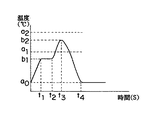
又、図5から図7に示す各値は、一例として、a0は室温、a1は接合材料の融点、本実施形態では接合材料は共晶半田であるので183℃、a2は230℃、b1は150℃、b2は220℃であり、t1は1秒、t2は3秒、t3は4秒、t4は10秒、t5は6秒である。
【0045】
特に電子部品6,7に加熱温度の制約がある場合、当該制約される加熱温度をa2としてこのa2以下に加熱上限温度b2を温度設定すれば良い。又、FPC5は、部品を実装していない上記裏面5bからのみ加熱されるため、電子部品6,7は最後に加熱されることになる。この点においても上記加熱制約があるときには有効である。
【0046】
又、半田溶融時における半田ボールの発生を抑える必要がある場合には、図5に示すように、同温を時刻t1から時刻t2まで維持する予熱動作を設けると好適である。一方、電子部品が比較的大きく半田ボールの影響が無視できるような場合では、図6に示すように、上記予熱動作を設けず、一気に半田を溶融させても良い。又、半田の溶融及び回路基板への電子部品の接合に要する時間の短縮を図りたい場合には、図7に示すように、予め予熱温度b1から開始して、半田接合終了後も温度b1を維持する方法も可能である。
【0047】
以上のように構成される電子部品接合装置101について、当該電子部品接合装置101の動作、つまり電子部品接合方法について以下に説明する。該電子部品接合方法、換言するとリフロー方法は、厚みが薄い回路基板に特に有効な方法であり、目安として1mm以下の厚みの基板に好適である。特に、本実施形態のように、フィルム状の回路基板、つまり上記FPC5は、温度制御に対する追従性が良く、より効果がある。回路基板の材質としては、1mm以下の回路基板ではガラスエポキシ樹脂や、紙フェノール樹脂が好ましく、フィルム状の回路基板ではポリイミドを用いたものが好ましい。これは0.01から0.1mm程度と非常に薄い回路基板でありながら、強度と耐熱性を併せ持っているからである。
【0048】
まず、回路基板、本例ではFPC5、に対応して上記吸着穴111が配置されている載置部材110をヒータ部121の載置部材設置面121aに置く。そして載置部材用吸引装置132を作動させ、ヒータ部121に開口する載置部材吸着用穴134を介して載置部材110を吸引し、載置部材110をヒータ部121に密着、固定する。次に、回路基板用吸引装置131を作動させた後、FPC5を載置部材110の表面110aに置き、ヒータ部121の回路基板吸着用穴133及び載置部材110の吸着穴111を介してFPC5を上記表面110aに密着、固定させる。この回路基板用吸引装置131によるFPC5の密着固定のための吸引は、例えば、圧力計131aにて検出される回路基板用吸引装置131による吸引圧力の100%値である0.9kPaに対して、90%値である0.8kPa程度の吸引圧力が検出されることでもって、上記密着固定の確認を行なうことができる。これによりヒータ部121に対し載置部材110が密着固定され、かつ載置部材110の表面110aにFPC5がなじんで密着保持され、ヒータ部121の熱が効率よくFPC5に伝わることになる。ヒータ部121による加熱動作は、上述した温度プロファイルに従い制御装置180により制御され、半田8が溶融して、FPC5上に電子部品6が半田にて接合される。該接合後、回路基板用吸引装置131の動作を停止して吸着を止め、載置部材110からFPC5が取り外される。
【0049】
上述した電子部品接合装置101によれば、加熱される一つの回路基板とほぼ同じ大きさにてなる載置部材110に上記回路基板を接触させて上記加熱装置120で加熱するようにしたことより、小型の回路基板に対してロスの発生を低減させることができ、かつ各種の回路基板に対応した加熱を個々に行うことができる。したがって、少量、多品種の回路基板について、従来に比べて高い生産性にて製造可能となる。
【0050】
具体的には、従来のリフロー炉においては、上記加熱に要する所定数量の回路基板当りの単位エネルギとして、20kW程度必要としていたのに対して、本第1実施形態の電子部品接合装置101においては、上記単位エネルギとして、1kW程度にまで削減することができる。
【0051】
又、加熱される一つの回路基板とほぼ同じ大きさにてなる載置部材110に上記回路基板を接触させて上記加熱装置120で加熱するようにしたことより、従来のような、雰囲気循環型のリフロー装置は不要となる。そして各電子部品接合装置101は、例えば35mm×35mmの大きさにてなるFPC5の場合、例えば35mm×35mmの大きさにて構成することができる。よって、従来に比べて非常にコンパクトな、回路基板の加熱接合装置を提供することができる。
【0052】
上述した実施形態の電子部品接合装置101では、載置部材110の表面110aには、一つのFPC5が載置され、載置部材110の大きさはFPC5の大きさと同じであるか、若しくは僅かに大きい。しかしながら、載置部材110に対する回路基板の大きさは、このような本実施形態の例に限定されるものではなく、例えば図8に示す電子部品接合装置102のように、上述の電子部品接合装置101を複数台、横方向に並設し、これら複数の載置部材110上に一つの回路基板を載置するようにしてもよい。又、並設する方向は、上記横方向に限定されるものではなく、縦方向、さらには縦、横両方向でもよい。又、一つの載置部材110の表面110aに複数のFPC5を載置してもよい。
【0053】
このように構成することで、回路基板の大きさに関係なく、本実施形態の電子部品接合装置101を適用することが可能となる。又、現状、セラミックスヒータ自体、大型のものがあまり存在せず、又、大型のセラミックスヒータの開発費が膨大であることに鑑みると、上述の並設構造は有効な手段である。
【0054】
又、上述の並設構造を採ることで、一つの回路基板における加熱領域の全域に対して一つの加熱制御を行うこともできるし、又、一つの回路基板における加熱領域内における複数の箇所においてそれぞれ異なる加熱制御を行うことも可能となり、汎用性を一層持ち合わせることができる。
【0055】
さらに又、より局部的に回路基板の加熱条件を変化させる必要がある場合には、図9に示す電子部品接合装置103のように、回路基板5の上方から光ビーム、レーザ、又はホットエア等を照射するように構成することもできる。尚、上述の図8及び図9では、上記電源部124、上記回路基板用吸引装置131、上記載置部材用吸引装置132、上記ヒータ部用冷却装置141、上記ベース部用冷却装置142、及び制御装置180の図示は、図1と同様に解せることから省略している。
【0056】
(第2実施形態)
次に、上述した電子部品接合装置101を用いて構成される電子部品実装装置(「実装システム」とも記載する)について説明する。尚、回路基板の一例として、上記FPC5を例にとる。
【0057】
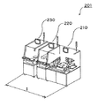
図11に示す上記実装システム201は、FPC5にクリーム半田8を塗布する半田供給装置210、FPC5へチップ部品6を装着する電子部品装着装置の一例である部品装着装置220、及び上記電子部品接合装置101を有し上記クリーム半田8を溶融させてチップ部品6をFPC5に接合させる加熱接合装置230を備え、半田供給装置210、部品装着装置220、加熱接合装置230の順にFPC5が搬送されるように、これらは配列されている。尚、上記IC7が予め実装されたFPC5が半田供給装置210に供給される。又、半田供給装置210は、半田印刷装置又は半田ディスペンス装置のいずれの構成でも良い。
【0058】
上述の電子部品接合装置101における説明にて述べたように、電子部品接合装置101では、回路基板を載置部材110上に吸着して加熱するように構成し、かつ一つの載置部材110の大きさは回路基板の大きさに対応していることから、上記加熱接合装置230の占める面積は、従来のリフロー装置に比べると格段に小さくなる。よって、上記実装システム201の全長Iは、本例の場合例えば約2.5mにおさめることができる。
【0059】
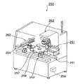
図10を参照して上記加熱接合装置230について説明する。
【0060】
加熱接合装置230は、上記電子部品接合装置101を備えた加熱部235と、前段の部品装着装置220からFPC5を当該加熱接合装置230に搬入するための搬入装置231と、当該加熱接合装置230からFPC5を次工程へ搬出するための搬出装置233と、上記搬入装置231から上記加熱部235へ、及び加熱部235から上記搬出装置233へFPC5の搬送を行う搬送装置232と、これらの構成部分の動作制御を行う制御装置236とを備える。
【0061】
上記搬入装置231には、上記FPC5を吸着保持し、搬送方向であるX方向へ駆動装置2311にて往復動する搬入台2312を備え、搬入装置231の動作は、制御装置236にて制御される。上記搬出装置233には、上記FPC5を吸着保持し、上記X方向へ駆動装置2331にて往復動する搬出台2332を備え、搬出装置233の動作は、制御装置236にて制御される。
【0062】
上記加熱部235は、第1ステージ235−1及び第2ステージ235−2の2つのステージから構成されており、第1ステージ235−1及び第2ステージ235−2のそれぞれは、図1に示す電子部品接合装置101を2台、縦方向、つまり図10に示すY方向に配列した構成にてなる。よって加熱部235では合計4台の電子部品接合装置101が使用されている。これは、当該実装システム201にて処理する1枚のFPC5が、電子部品接合装置101の上記載置部材110を2つ上記Y方向に並べた大きさに相当するからである。尚、当該実装システム201にて処理するFPC5の具体的なサイズは、35mm×70mmである。このように、上記ステージのサイズは、当該実装システム201の形態に限定されるものではなく、処理する回路基板の大きさに応じて決定すればよい。又、加熱部235に設ける上記ステージの数も本例に限定されるものではなく、一つ以上であればよく、実装システムに対して要求される処理能力に基づいて決定される。
【0063】
又、図10では、それぞれの上記ステージ235−1、235−2を構成する各電子部品接合装置101に備わる上記電源部124、上記回路基板用吸引装置131、上記載置部材用吸引装置132、上記ヒータ部用冷却装置141、及び上記ベース部用冷却装置142の図示は、図1と同様に解せることから省略しており、又、上記制御装置180は制御装置236に代わる。したがって、第1ステージ235−1及び第2ステージ235−2のそれぞれについて、上述した、制御装置180による電子部品接合装置101に対する温度制御と同じ温度制御が制御装置236の動作制御により実行される。
【0064】
上記搬送装置232は、上記搬入装置231の搬入台2312から上記加熱部235の第1ステージ235−1及び第2ステージ235−2へFPC5を搬送する搬入吸着装置2321と、第1ステージ235−1及び第2ステージ235−2から上記搬出装置233の搬出台2332へFPC5の搬送を行う搬出吸着装置2322と、上記搬入吸着装置2321及び上記搬出吸着装置2322を設けた搬送アーム2323を、FPC5の厚み方向でありX方向及びY方向に直交するZ方向へ移動させるZ−駆動装置2324と、該Z−駆動装置2324をY方向へ移動させるY−駆動装置2325と、該Y−駆動装置2325をX方向へ移動させるX−駆動装置2326と、を備える。又、上記搬入吸着装置2321及び上記搬出吸着装置2322には、図示を省略している、吸引装置が含まれる。このような構成を有する搬送装置232は、制御装置236にて動作制御される。
【0065】
さらに、当該加熱接合装置230には、加熱部235にて加熱中のFPC5から発生するヒュームを吸引するダクト2341を有する吸引装置234を備えている。
【0066】
以上のような構成を有する実装システム201における動作について、加熱接合装置230における動作を中心に、以下に説明する。
【0067】
部品装着装置220から搬送されたFPC5は、加熱接合装置230に備わる搬入装置231の搬入台2312上に供給される。搬送装置232に備わるX−駆動装置2326、Y−駆動装置2325、Z−駆動装置2324、及び搬入吸着装置2321がそれぞれ駆動され、FPC5は、搬入吸着装置2321にて吸着保持されて加熱部235の第1ステージ235−1上に載置され、吸着保持される。そして、FPC5は、第1ステージ235−1上に保持されながら、上記加熱装置120によって上記温度プロファイルに基づいて加熱、つまりリフロー動作が行われる。該加熱中に発生するヒュームは、吸引装置234のダクト2341で吸引される。
【0068】
次に当該加熱接合装置230に搬入される第2番目のFPC5も、上記第1番目のFPC5と同様に取り扱われるが、該第2番目のFPC5は、現在空いている第2ステージ235−2へ供給され、加熱、温度制御され、FPC5と上記チップ部品6との接合がなされる。さらに次の第3番目のFPC5については、搬入吸着231で吸着しておき、最初に搬送した第1番目のFPC5について第1ステージ235−1での加熱が終了し搬送装置232の搬出吸着装置2322にて第1ステージ235−1から搬出装置233の搬出台2332へ取り出された後、直ちに第1ステージ235−1へ供給され加熱される。
【0069】
上記搬出台2332へ載置され吸着されているFPC5は、保持され次工程へ搬出される。以上の動作を繰り返すことで、順次、FPC5が処理される。
【0070】
上述の加熱接合装置230を備えた実装システム201によれば、加熱接合装置230は、上述したように、従来に比べて非常にコンパクトに構成されることから、実装システム201の全体を従来に比べてコンパクト化することができる。
【0071】
上述の実装システム201は、図11に示すように、半田供給装置210、部品装着装置220、及び加熱接合装置230を、回路基板の搬送方向、つまり上記X方向に沿って列状に配置した構成にてなるが、実装システムの全体構成は上述の形態に限定されるものではなく、図12に示すようなロータリータイプの実装システム250を構成することもできる。
【0072】
上記実装システム250には、円形状で周縁部に作業部258を一定間隔にて設けたロータリーテーブル257が当該実装システム250の中央部分に間欠回転可能に装備され、該ロータリーテーブル257を取り囲みかつ上記作業部258の停止位置に対応して、回路基板へ半田を供給する半田供給装置261と、半田が供給された回路基板へチップ部品6を装着する部品装着装置262と、上述の電子部品接合装置101を備え上記半田を加熱し回路基板に上記チップ部品6を接合させる加熱接合装置263とが配置され、さらに当該実装システム250全体の動作制御を司る制御装置256が備わる。さらに又、前工程から当該実装システム250へ回路基板を搬入するための搬入装置251、当該実装システム250から次工程へ回路基板を搬出する搬出装置253、及び回路基板を上記作業部258へ搬送する搬送装置252も備わる。又、回路基板の加熱中に発生するヒュームを吸引する吸引装置も設けられている。
【0073】
このように構成される実装システム250は以下のように動作する。
【0074】
上記搬入装置251を介して回路基板が搬送装置252にて作業部258に載置され、ロータリーテーブル257の回転により半田供給装置261へ搬送される。半田供給装置261では、回路基板に半田が供給される。そして再びロータリーテーブル257が回転し、回路基板は部品装着装置262へ搬送される。部品装着装置262では、半田が供給されている回路基板へ上記チップ部品6が装着される。そして再びロータリーテーブル257が回転し、回路基板は加熱接合装置263へ搬送される。加熱接合装置263では、回路基板の加熱そして回路基板への部品の接合が行われる。そして再びロータリーテーブル257の回転により回路基板は搬出装置253へ搬送され、搬送装置252にて搬出装置253へ載置される。搬出装置253は回路基板を次工程へ搬出する。
【0075】
尚、例えば、第1番目の回路基板が加熱接合装置263にて加熱されているとき、第2番目の回路基板には部品装着装置262にて部品装着がなされ、第3番目の回路基板には半田供給装置261にて半田が供給される。このように複数の回路基板に対してそれぞれ異なる処理が同時になされる。
【0076】
上記実装システム250のように、ロータリーテーブル257を備えた形態を採ることで、実装システム250の横幅をさらに小さくすることができる。
【0077】
又、ロータリーテーブル257の停止位置を8分割にすると、半田供給装置261と部品装着装置262との間に、回路基板への半田の供給状態を検査するための認識カメラや、半田供給不備部分への半田追加用の装置をさらに設けることができ、有効活用することができる。又、加熱接合装置263は、作業部258内や、搬出装置253や、ロータリーテーブル257と搬出装置253との間に設けることもできる。
【0078】
上述した各実施形態では、回路基板としてFPC5を例に採っているので、回路基板の搬送は、回路基板を吸着保持する方法を採っている。しかしながら、回路基板が例えば1mm程度の厚みを有しかつ撓み等の変形が生じ難い基板である場合、図13に示すように、ブラケット301で支持された搬送レール302で回路基板310を搬送するように構成しても良い。この場合、加熱接合装置120は、上下駆動部303で回路基板310に密着させるが、該密着を安定させるために、搬送レール302に押さえ部材304を設けておくと良い。具体的には、図13における回路基板310の図示左右両端部を夫々の押さえ部材304により押さえることにより、回路基板310の下面をヒータ部121の上面に密着させることができる。
【0079】
(第3実施形態)
上述したように、各実施形態において使用される電子部品接合装置101では、FPC5は、回路基板用吸引装置131による吸引動作により載置部材110の表面110aに吸着保持されるが、そのための吸引用通路は、図4に示すようにヒータ部121を通過して上記回路基板用吸引装置131に至る。よって、載置部材110に吸着されているFPC5が加熱され、クリーム半田8が溶融したときに生じるヒュームの一部が上記吸引によりヒータ部121へ流れ込む可能性がある。又、載置部材110に吸着される回路基板には、該基板の厚み方向に沿って当該基板を貫通するスルーホールが形成された種類の回路基板もある。このようにスルーホールを有する回路基板では、ヒータ部121を通過するヒューム量は非常に多くなる。
【0080】
ヒータ部121に上記ヒュームが流入することで、ヒータ部121の清掃が必要となり、清掃作業のため設備を停止せざるを得ず、生産性の低下を招く結果となる。
【0081】
そこで以下に説明する第3実施形態における電子部品接合装置は、上述の第1実施形態における電子部品接合装置101の改良型であって、上記ヒュームの影響を防止し生産性の向上を図るものである。又、第2実施形態にて説明した実装システム201において、電子部品接合装置101に代えて以下の第3実施形態の電子部品接合装置を備えた構成を採ることもできる。
【0082】
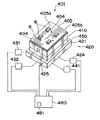
図14に示されたフレキシブル基板(FPC)405は、上述のFPC5と同様に、例えば液晶モジュールとマザー基板との接続を行うための基板であり、片面実装基板であり、当該FPC405の電子部品実装面405a(電子部品装着面の一例である)には、未硬化のクリーム半田8が塗布された箇所に複数の電子部品6やIC7が搭載されている。又、本実施形態では、FPC405の厚み方向に当該FPC405を貫通して複数のスルーホール貫通穴404が形成されている。又、上記部品実装面405aに対向する、当該FPC405の載置部材接触面405bにおいて配線が存在しない部分に対応して、上記配線のおよそ厚み分にて図16に示す凹部405cが形成される。上記スルーホール貫通穴404は、不要配線部分を断線する目的で設けられることから、通常、スルーホール貫通穴404と上記凹部405cとはつながった構造となる。
【0083】
第3実施形態における電子部品接合装置401は、図14に示すように、上記FPC405を載置する載置部材410と、該載置部材410を加熱して載置部材410に接触しているFPC405を加熱し、これにより部品をFPC405に接合するクリーム半田8を溶融させる加熱装置420とを備え、又、上記載置部材410と加熱装置420とに挟まれて配置される密着用部材450を有するのが好ましい。
【0084】
図15に示された載置部材410は、上述の載置部材110に相当する部材であり、FPC405を載置し保持する機能と、FPC405に熱を伝える機能とを併せ持ち、各種の回路基板に対応可能となるように容易に交換可能である。当該載置部材410は、アルミニウム、銅、マグネシウム、セラミック等の熱伝導性に優れた材料にてなるものが好ましい。特に3mm程度の厚みのアルミニウム材を用いると、安価で均熱性も図られ好適である。本実施形態では、当該載置部材410は、処理するFPC405の大きさに対応して、45mm×80mmの長方形の板材にてなる。
【0085】
さらに、FPC405の上記載置部材接触面405bが接する当該載置部材410の回路基板載置面410aには、FPC405を吸着保持するための複数の基板吸着穴411が開口している。本実施形態では、図16に示すように、基板吸着穴411は、FPC405に形成されているスルーホール貫通穴404と直接に連通するのを避けた位置に配置している。さらに、図16に示すように基板吸着穴411は、FPC405の載置部材接触面405bの凹部405cにもつながらない位置に配置されている。尚、このような配置条件を満たす限り、基板吸着穴411の数及び配置位置は、保持する回路基板に応じて決定すればよい。よって、基板吸着穴411は、上記載置部材接触面405bにおける、凹部405c及びスルーホール貫通穴404以外の吸着領域405dを吸着する。尚、該吸着領域405dは、通常平坦面であるが、凹状であってもよい。
【0086】
又、各基板吸着穴411は、上記基板載置面410aに対向する、当該載置部材410の密着用部材接触面410bに形成されている基板吸着溝412を介してつながっており、該基板吸着溝412は、載置部材410の側面410cに形成した吸引用開口415につながっている。該吸引用開口415は、回路基板用吸引装置431に直接接続される。よって、載置部材410の基板載置面410aに載置されているFPC405は、回路基板用吸引装置431の吸引動作により、基板載置面410aに吸着され保持される。又、上述のように、基板吸着穴411及び基板吸着溝412は、スルーホール貫通穴404の形成位置と合致しないように配置されて形成されていることにより、部品6の接合時にクリーム半田8から生じるヒュームについて、スルーホール貫通穴404を通して基板吸着穴404及び基板吸着溝412に流入することが防止されているが、仮に、上記スルーホール貫通穴404を通して基板吸着穴411及び基板吸着溝412に上記ヒュームが流入するような場合が発生しても、上記ヒュームは、上記吸引用開口415を介して回路基板用吸引装置431にて吸引される。このように第3実施形態では、上記ヒュームは、加熱装置を通過しない。
【0087】
又、スルーホール貫通穴404と基板吸着穴411とは直接につながっていないので、又、基板吸着穴411は上述のように吸着領域405dを吸着することから、基板吸着穴411による基板載置面410aへのFPC405の保持力は大きく、保持精度の向上を図ることができる。さらに、基板載置面410aに対してFPC405は、基板吸着穴411による局所的な吸引により保持されることから、基板載置面410aに例えば溝状に設けた吸引穴にて吸引する場合に比べてエアーリーク量を低減させることができる。よってこの点からも、基板載置面410aへのFPC405の保持精度の向上を図ることができる。
【0088】
さらに又、載置部材410の密着用部材接触面410bには、上記密着用部材450を間に挟み載置部材410をヒータ部421に密着保持させるための載置部材用吸着溝413が上記基板吸着溝412とは別個に設けられている。尚、載置部材用吸着溝413は、図示するように本実施形態では円形状の凹部にてなるが、その直径は、後述のヒータ部422に形成される載置部材吸引用通路422の直径よりも大きくしている。
【0089】
図17に示すように、密着用部材450は、載置部材410の汚れがヒータ部421に及ばないよう遮断する機能と、載置部材410に熱を伝える機能とを併せ持つシート状の部材であり、メンテナンス作業効率の向上のため容易に交換可能に構成される。密着用部材450は、アルミニウム、銅、マグネシウム、セラミック等の熱伝導性に優れた材料にてなるのが好ましい。特に0.05mm程度の厚みのアルミニウム材を用いると、安価で均熱性も図られ好適である。本実施形態では、密着用部材450は、処理するFPC405の大きさに対応して、45mm×80mmの長方形にてなる。又、図示するように、密着用部材450には、載置部材410の密着用部材接触面410bに存在する載置部材用吸着溝413と同一形状で同位置に、載置部材吸着穴451が当該密着用部材450の厚み方向に貫通して形成されている。尚、載置部材用吸着溝413及び載置部材吸着穴451にて、吸着用空間を構成する。
【0090】
このような密着用部材450を設けることで、載置部材410と下記ヒータ部421との密着性の向上を図るとともに、載置部材410の基板吸着溝412がヒータ部421に直接に接するのを防止して上記ヒュームがヒータ部421に付着するのを防止することができる。
【0091】
図18に示すヒータ部421は、昇降温に対する応答性が優れているセラミックヒータにてなり、電源部424からヒータ線へ電流が供給され発熱する仕組みとなっている。尚、上記ヒータ部421及び電源部424にて加熱装置420を構成している。本実施形態では、ヒータ部421は、0.5mmから5mm程度の厚さで、窒化珪素セラミック、コージライト、窒化アルミセラミック等の均熱性、熱伝導性に優れた材料にてなるものが好ましい。特に2mm程度の厚みの窒化珪索セラミック材を用いると、安価で均熱性も図られ好適である。本実施形態では、ヒータ部421は、処理するFPC405の大きさに対応して、55mm×90mmの長方形にてなる。又、ヒータ部421には、密着用部材450の載置部材吸着穴451に対応する位置にて、当該ヒータ部421をその厚み方向に貫通する載置部材吸引用通路422が形成されている。該載置部材吸引用通路422には、載置部材用吸引装置432が接続されている。よって、載置部材用吸引装置432が作動することで、載置部材吸引用通路422、載置部材吸着穴451、及び載置部材用吸着溝413の空気が吸引され、ヒータ部421の載置面421aに、密着用部材450を間に挟んで載置部材410が密着して吸着される。
【0092】
又、載置部材吸引用通路422は、本実施形態では円筒形の通路であるが、その直径を、上述した載置部材用吸着溝413及び載置部材吸着穴451に比して小さくしている。このように構成することで、載置部材吸引用通路422に対して、載置部材410において、より大きな吸着用空間つまり上記載置部材用吸着溝413を確保し、ヒータ部421への載置部材410の保持力の向上を図ることができる。
【0093】
ヒータ部421の温度は、温度センサ、例えばヒータ部421内に設けた熱電対425にて測定され、制御装置480へ送出される。電源部424は、制御装置480に接続されており、制御装置480は、熱電対425から供給される温度情報と、回路基板の温度制御用として予め設定された温度プロファイルとに基づいてヒータ部421の温度をフィードバック制御する。又、上記温度プロファイルに沿った温度制御を行うため、強制的にヒータ部421の冷却が可能なようにヒータ部421にはヒータ部用冷却装置441が接続されている。該ヒータ部用冷却装置441は、本実施形態では、気体、例えば空気をヒータ部421に供給し、ヒータ部121を強制的に冷却する。
【0094】
制御装置480は、上述した回路基板用吸引装置431、載置部材用吸引装置432、電源部424、及びヒータ部用冷却装置441に接続され、記憶部481に格納したプログラムに従い、これらの各構成部分の動作制御を行う。
【0095】
以上のように構成される電子部品接合装置401について、当該電子部品接合装置401の動作、つまり電子部品接合方法について以下に説明する。該電子部品接合装置401は、上述した電子部品接合装置101における場合と同様に、厚みが薄い回路基板を加熱保持するのに特に有効であり、目安として1mm以下の厚みの基板に好適である。
【0096】
まず、ヒータ部421の載置部材吸引用通路422に、密着用部材450の載置部材吸着穴451を対応させて、ヒータ部421の載置面421aに密着用部材450を載置する。さらに、載置部材吸着穴451に、載置部材410の載置部材用吸着溝413を対応させて、該密着用部材450上に載置部材410を載置する。そして、載置部材用吸引装置432を作動させて吸引動作にて、ヒータ部421の載置面421aに、密着用部材450を間に挟んで載置部材410を密着保持させる。次に、回路基板用吸引装置431を作動させた後、FPC405を載置部材410の回路基板載置面410aに置き、載置部材110の基板吸着穴411及び基板用吸着溝412を介してFPC405を上記回路基板載置面410aに密着、固定させる。
【0097】
ヒータ部421による加熱動作は、上述した温度プロファイルに従い制御装置480により制御される。該加熱動作により、クリーム半田8が溶融して、FPC405上に電子部品6が半田にて接合される。
【0098】
このとき、クリーム半田8から生じるヒュームは、FPC405のスルーホール貫通穴404を通り吸引されることもあるが、吸引されたヒュームは、載置部材110の基板吸着穴411及び基板用吸着溝412を通り排出されることから、ヒータ部421を汚すことはない。このように第3実施形態の電子部品接合装置401によれば、ヒータ部421の清掃は不要であり、清掃作業のため設備を停止することはなく、高い生産性を達成することができる。例えば、従来の装置では、ヒータ部の清掃として、装置運転時間24時間に対して、1回の清掃作業が必要であり、当該清掃作業に40分程度要し、その間装置を稼動させることができないという問題があるのに対して、本第3実施形態の電子部品接合装置401においては、ヒータ部421の清掃は行なったとしても、装置運転時間2〜3日に対して、1回の清掃作業を行なう程度で十分である。さらに、当該清掃作業は布等によるヒータ部421の表面の拭き取り作業程度となるため、数分間の作業となり装置の稼動に影響を与えることはない。
【0099】
上述のようにしてFPC405への部品6の接合が終了した後、回路基板用吸引装置431の動作を停止して吸着を止め、載置部材410からFPC405が取り外される。
【0100】
上述した電子部品接合装置101の場合と同様に、当該電子部品接合装置401においても、載置部材410の回路基板載置面410aに一つのFPC405が載置されるように、載置部材410の大きさはFPC405の大きさと同程度か、若しくは僅かに大きい。しかしながら、載置部材410に対する回路基板の大きさは、このような本実施形態の例に限定されるものではなく、図8を参照して説明したように、例えば上述の回路基板吸着保持装置401を複数台併設し、これら複数の載置部材410上に一つの回路基板を載置するようにしてもよい。
【0101】
(第4実施形態)
次に、本発明の第4実施形態にかかる電子部品接合装置の一例について説明する。本第4実施形態にかかる上記電子部品接合装置は、その基本的な構成は、上記第3実施形態の電子部品接合装置401と同様であるが、その載置部材における基板吸着穴の配置を電子部品の配置と関係させているという特徴を有している点において相違している。以下、この上記基板吸着穴の配置等の特徴に関する説明を図22を用いて説明する。
【0102】
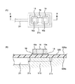
図22は、載置部材510と、当該載置部材510の上面である回路基板載置面510aに載置されるFPC505との関係を示す図であり、図22(A)は、電子部品6が装着された状態のFPC505の部分断面模式図であり、図22(B)は、載置部材510の部分断面模式図である。
【0103】
図22(A)に示すように、FPC505は、その上面である電子部品実装面505a(電子部品装着面の一例である)において、電子部品6が接合材料の一例であるクリーム半田8を介して装着されている。一方、FPC505における電子部品実装面505aと反対側の面である載置部材接触面505bにおいては、電子部品実装面505aにおけるクリーム半田8の配置領域に対応する領域である接合材料配置領域の一例である半田配置領域505eが設けられている。さらに、FPC505の載置部材接触面505bには、半田配置領域505eに隣接して配置された領域である吸着領域505dが設けられている。なお、この夫々の吸着領域505dにおいて、図示しない回路基板用吸引装置によりFPC505が吸着されることが可能となっている。また、夫々の吸着領域505dは、半田配置領域505eに重なることなく隣接して配置されているため、これらの吸着領域505dに対応する電子部品実装面505aにおける領域は、クリーム半田8の配置領域と重なることなく、隣接されて配置されている。
【0104】
また、図22(B)に示すように、載置部材510の回路基板載置面510aにおいては、FPC505が載置された場合に、FPC505の載置部材接触面505bにおける半田配置領域505eと接触して、当該接触による伝熱(すなわち、図示しない加熱ヒータの加熱による載置部材510を介しての伝熱)を行なうことができる伝熱部510bが形成されている。また、載置部材510の回路基板載置面510aには、この伝熱部510bに隣接するように基板吸着穴511が設けられており、また、夫々の基板吸着穴511の形成位置は、FPC505の載置部材接触面505bにおける夫々の吸着領域505dに対応している。
【0105】
このように、FPC505の載置部材接触面505bにおいて、半田配置領域505eと吸着領域505dとが設けられていること、及び、載置部材510の回路基板載置面510aにおいて、伝熱部510bと基板吸着穴511とが形成されていることにより、FPC505の載置部材接触面505dを、載置部材510の回路基板載置面510aに重ねるように載置した場合に、伝熱部510bと半田配置領域505eとを互いに接触させるように、図示しない回路基板用吸引装置に接続された夫々の基板吸着穴511でもって、夫々の吸着領域505dを吸着することができる。これにより、FPC505に反りや曲がりが生じているような場合であっても、半田配置領域505eの近傍に配置されている吸着領域505dを吸着することで、半田配置領域505eを伝熱部510bに確実に密着させることができ、伝熱部510bより半田配置領域505eへの伝熱効率を良好なものとすることができる。特に、FPC505が可撓性を有するというその機能特性により、載置部材510により吸着保持するような場合であっても、反りや曲がりが部分的に発生し、良好な吸着を行なうことができないような場合が考えられるが、このような場合であっても、電子部品6を接合すべき領域である半田配置領域505eのの近傍を吸着することで、他の領域での反りや曲がりの発生の有無に拘らず、半田配置領域505eを確実に伝熱部510bに接触されることができる。
【0106】
また、夫々の吸着領域505dは加熱する必要がない領域であるため、基板吸着穴511による吸着が行なわれて、伝熱が行なわれなくても、クリーム半田8の加熱溶融のための伝熱に対しての問題は生じない。従って、FPC505において、加熱をしなければならないクリーム半田8に確実かつ効率的に伝熱による加熱を行うことができる。なお、夫々の基板吸着穴511の形成幅は、載置部材510よりのFPC505への伝熱や、夫々の基板吸着穴511によるFPC505の吸着を考慮して、0.5mm〜1.0mm程度とすることが好ましい。また、半田配置領域505eと伝熱部510bとの確実な接触を行なうための吸着という観点から、夫々の吸着穴511の形成位置は、半田配置領域505eの端部から1,5mm程度離れた位置までの間に形成されることが好ましい。
【0107】
次に、このようなFPC505と載置部材510との配置関係の特徴を利用した、具体的な基板吸着穴511の配置例について、いくつかの実施例を用いて以下に説明する。なお、以降の夫々の実施例の説明においては、その説明の理解を容易とするために、電子部品と基板吸着穴等との配置関係に特に着目した図を用いるものとするが、これらの説明や図は、上記特徴を概念的に示す図22に基づいても理解されるものである。
【0108】
まず、図23(A)〜(C)に、FPC505の電子部品実装面505a側から見た電子部品と基板吸着穴との配置関係を示す模式平面図を示す。
【0109】
図23(A)に示すように、電子部品の一例であるチップ部品16は、その両端部に夫々電極部16aを備えており、FPC505の電子部品実装面505a(共に図示を省略している。以下、同じ)に配置形成された接合材料の一例である夫々の半田部18を夫々の電極部16aが介するように、チップ部品16がFPC505に装着されている。
【0110】
一方、載置部材510の回路基板載置面510a(共に図示を省略している。以下、同じ)には、図23(A)に示すように、基板吸着穴の一例であって、その表面に沿って溝状に形成された穴である基板吸着用溝部21が形成されている。この基板吸着用溝部21は、その上面全体が開口されており、図示しない回路基板用吸引装置に接続されて吸引されることにより、上記開口全体で、FPC505を吸着することが可能となっている。
【0111】
また、図23(A)に示すように、基板吸着用溝部21は、2つの基板吸着用溝部21a及び21bに分岐されており、基板吸着用溝部21aが、FPC505の電子部品実装面505aへのチップ部品16の投影された外形形状における長手方向の辺に、平行に略直線的に延在するように配置されるとともに、基板吸着用溝部21bが、上記外形形状における短い辺に平行に略直線的に延在するように配置されている。なお、夫々の基板吸着用溝部21a及び21bの配置位置は、夫々の半田部18の形成位置に近接するように配置されていいるものの、夫々の半田部18の上記形成位置とは互いに重なることはないように配置されている。
【0112】
このようにFPC505におけるチップ部品16の配置位置に関連させて、載置部材510に基板吸着用溝部21a及び21bが配置されて形成されていることにより、夫々の半田部18が配置形成されている領域に対応する領域(載置部材接触面505bにおける領域)を半田配置領域505e(図22参照)とし、夫々の基板吸着用溝部21a及び21bにより吸着される領域(載置部材接触面505bにおける領域)を吸着領域505d(図22参照)とすることができる。従って、夫々の基板吸着用溝部21a及び21bにて、夫々の吸着領域505dを吸着することにより、半田配置領域505eを載置部材510の回路基板載置面510aに確実に接触させることができ、載置部材510を介しての半田配置領域505eへの伝熱を確実に行なって、夫々の半田部18の加熱溶融を効率的に行なうことができる。また、基板吸着用溝部21a及び21bの上面全体が開口されていることにより、その吸着領域505dを拡大することあできるため、安定した吸着を実現することができる。さらに、基板吸着用溝部21a及び21bが略直線的に形成されていることより、その形成を容易なものとすることができるとともに、メンテナンスの際における清掃等の作業性を良好なものとすることができる。
【0113】
次に、図23(B)及び(C)は、図23(A)と同様なチップ部品16を用いるものの、その基板吸着用溝部21の配置が異なる例を示したものである。図23(B)においては、チップ部品16の上記投影された外形形状における長手方向の夫々の辺に平行にかつ略直線的に、2つの基板吸着用溝部21a及び21bが配置されており、図23(C)においては、上記外形形状における夫々の短い辺に平行に、2つの基板吸着用溝部21a及び21bが配置されている。図23(B)及び(C)のように、夫々の基板吸着用溝部21a及び21bが配置形成されるような場合であっても、上記図23(A)の場合と同様な効果を得ることができるとともに、夫々の基板吸着用溝部21aと21bとが互いに平行に配置形成されていることより、FPC505の吸着をより安定して行なうことができる。
【0114】
次に、図24(A)に、FPC505の電子部品実装面505a(図22参照)側から見たチップ部品16と基板吸着用溝部21との配置関係を示す模式平面図を示し、図24(A)におけるX−X断面における矢視断面図を図24(B)に示す。
【0115】
図24(A)に示すように、載置部材510の回路基板載置面510aに形成されている基板吸着用溝部21cは、図23の場合とは異なり、チップ部品16の上記外形形状の夫々の辺と平行にかつ略直線的に、上記外形形状を取り囲むように形成されている。このようにチップ部品16の上記外形形状を取り囲むように形成されていることにより、その内側に配置される半田配置領域505e(図22参照)をより均等な力でもって確実に載置部材510の回路基板載置面510aに接触させることができる。従って、載置部材510よりFPC505を介して夫々の半田部18に確実に伝熱して加熱することができ、夫々の半田部18の加熱溶融をより確実に行なうことができる。
【0116】
また、このように基板吸着用溝部21cが、チップ部品16の上記外形形状を取り囲むように配置形成されていることにより、その吸着領域505d(図22参照)の面積も大きくなって、これに対応して図示しない回路基板用吸引装置による吸引流量も増大する。このような吸引流量の増大に対応するために、図24(B)に示すように、基板吸着用溝部21cに接続して形成されている基板吸着用溝部21の形成深さが、基板吸着用溝部21cの形成深さよりも深くなるように、例えば、基板吸着用溝部21cの形成深さの2倍程度の深さとなるように、基板吸着用溝部21が形成されている。これにより、上記吸引流量の増大に対応することが可能となるとともに、基板吸着用溝部21cの上記吸引における流速が、基板吸着用溝部21の流速よりも大きくすることができ、基板吸着用溝部21cによるFPC505の吸着力を、基板吸着用溝部21の吸着力よりも大きくすることができる。よって、半田配置領域505eの周囲をより高い吸着力にて吸着して、半田配置領域505eをより確実に載置部材510の回路基板載置面510aに接触させることができ、上記伝熱における効率や確実性を高めることができる。
【0117】
なお、図24においては、基板吸着用溝部21の形成幅を変えずに、その形成深さを深くすることで、上記吸引流量の増大に対応しているが、このような場合にのみ限定されるものではない。例えば、図25に示すように、チップ部品16を取り囲むように形成されている基板吸着用溝部21cに接続されている基板吸着用溝部21dのように、その形成幅を基板吸着用溝部21cより大きくすることで、上記吸引流量増大に対応するような場合であってもよい。例えば、基板吸着用溝部21cの形成幅を、0.5mm程度として、これに対して、基板吸着用溝部21dの形成幅を、1.0mm程度とする。また、例えば、図26に示すように、基板吸着用溝部21cに接続されている基板吸着用溝部を、複数の、例えば、2つの基板吸着用溝部21eとして形成することで、上記吸引流量増大に対応するような場合であってもよい。
【0118】
なお、上記においては、チップ部品16の上記外形形状の周囲を吸着する基板吸着用溝部21cの吸引における流速が、その他の基板吸着用溝部21よりも大きくなるように形成されることについて説明したが、この流速は、載置部材510における上記吸引の経路、すなわち、図16に示される基板吸着溝412や吸引用開口415における流速よりも大きくなるように設定されることが望ましい。FPC505を吸着する位置にて、その吸引により流速を最大として吸着力を高めることにより、FPC505の吸着を確実なものとすることができるからである。
【0119】
次に、FPC505に複数のチップ部品16が装着配置された場合の基板吸着用溝部21の配置について、図27を用いて説明する。
【0120】
図27に示すように、複数のチップ部品16が整列配置されて狭隣接装着されているような場合にあっては、夫々のチップ部品16の間に個別に基板吸着用溝部21を形成することが困難な場合も少なくない。
【0121】
このような場合にあっては、図27に示すように、夫々のチップ部品16の整列配置の方向(すなわち、図示上下方向)に沿って略直線的に、夫々のチップ部品16をFPC505の表面に沿ってに挟むように、2つの基板吸着用溝部21a及び21bを互いに平行に配置形成する。これにより、夫々の基板吸着用溝部21a及び21bで挟まれた領域全体を、半田配置領域505eとみなして、この半田配置領域505eを載置部材510の回路基板載置面510aに接触させることで、伝熱加熱を行ない、夫々の半田部18の加熱溶融を行なうことができる。
【0122】
さらに、図28に示すように、夫々のチップ部品16が2列に整列配置されているような場合にあっては、夫々の整列配置の方向に沿って3つの基板吸着用溝部21a、21b、及び21cを形成することもできる。なお、図28に示すような夫々のチップ部品16の配置においては、例えば、図示左右方向に延在するように、夫々の基板吸着用溝部を配置することもできるが、このような場合であっても、半田配置領域505eを確実に載置部材510の回路基板載置面510aに接触させるために、夫々の基板吸着用溝部の間隔が広くなりすぎないことが望ましい。すなわち、図28における図示上下方向又は左右方向のいずれにも夫々の基板吸着用溝部を配置することができるような場合にあっては、夫々の基板吸着用溝部の間隔が狭くなるような配置を選択することが望ましい。
【0123】
あるいは、図29に示すように、チップ部品16の整列配置されている領域の両端部に、上記整列配置の方向沿いに2つの基板吸着用溝部21a及び21bを配置させて、夫々のチップ部品16の整列配置の列の間には、基板吸着穴21fを形成するような場合であってもよい。
【0124】
図28及び図29のいずれの場合であっても、夫々の基板吸着用溝部21a、21b、21cや、基板吸着穴21fにより、夫々のチップ部品16が配置されている領域を、確実に載置部材510の回路基板載置面510aに接触させることができ、当該接触によりFPC505を介しての夫々の半田部18の伝熱加熱を確実に行なうことができる。
【0125】
また、図30に示すように、互いに離間された2箇所の半田部18にてFPC505に整列配置されている夫々のチップ部品16に対しては、上記整列配置の方向沿いであって、夫々の半田部18の間に配置されるように、基板吸着用溝部21を形成することができる。このような場合にあっては、夫々の半田部18が形成されている領域が半田配置領域505eとなって、夫々の半田配置領域505eの間に吸着領域505dが配置されることとなる。
【0126】
このような基板吸着用溝部21の配置は、特に、夫々のチップ部品16の整列配置領域の周囲に、吸着領域505dが配置できないような場合に有効である。それとともに、実質的には、チップ部品16の真下でFPC505の吸着を行なうことができるため、夫々の半田部18の溶融のためのFPC505の吸着を安定して行なうことができる。
【0127】
また、図31に示すように、夫々のチップ部品16が整列配置されていないような場合であっても、夫々のチップ部品16が配置されている領域に沿って、2つの基板吸着用溝部21a及び21bが配置形成されるような場合であってもよい。
【0128】
次に、電子部品の一例としてQFP26がFPC505に装着されている場合における基板吸着用溝部の配置について、図32から図34を用いて以下に説明する。
【0129】
図32は、QFP26の模式的な構造を示す模式斜視図であるが、図32に示すように、QFP26は、その略正方形板状のパッケージを有する4辺に、端子部である複数のリード26aが設けられており、夫々のリード26aがFPC505に半田部28を介して装着されるという構成を有している。
【0130】
また、図33に示すように、FPC505の電子部品実装面505a(図22参照)においては、電子部品実装面505aへのQFP26の投影された外形形状の外周に沿って、複数の半田部28が形成されており、QFP26における夫々のリード26aは、夫々の半田部28に接続されている。また、夫々の半田部28の上記配置位置の外周に平行に、夫々の半田部28を取り囲むように、基板吸着用溝部21gが形成されている。このように基板吸着用溝部21gが形成されることにより、その内側の領域である夫々の半田部28の形成領域全体を、半田配置領域505e(図22参照)と見なして、この半田配置形成領域505eを載置部材510の回路基板載置面510aに確実に接触させることができる。よって、確実かつ効率的な夫々の半田部28の溶融を行なうことができる。
【0131】
また、図33においては、夫々の半田部28の配置位置の外周に基板吸着用溝部21gを形成する場合について説明したが、このような場合にのみ限定されるものではなく、例えば、図34に示すように、夫々の半田部28の上記配置位置の内周に基板吸着用溝部21hを形成するような場合であってもよい。上記内周における領域においても、FPC505を加熱する必要が無いため、吸着領域505d(図22参照)として利用することができるからである。なお、このような場合にあっては、上記内周に形成されている基板吸着用溝部21hに接続される基板吸着用溝部21は、夫々の半田部28が形成されていない位置、例えば、QFP26の夫々の隅部分に、位置されるように形成されることが望ましい。夫々の半田部28への伝熱に影響を与えないためである。
【0132】
なお、QFP26のサイズが大きく、より高い吸着力でもって確実に吸着する必要があるような場合にあっては、図33と図34とを組み合わせて、夫々の半田部28の配置位置の外周に基板吸着用溝部21gを、内周に基板吸着用溝部21hを、共に形成するような場合であってもよい。
【0133】
次に、電子部品の一例として、ベアIC36がFPC505に配置されているような場合における基板吸着穴の配置等について、図35を用いて説明する。
【0134】
図35(B)は、ベアIC36の模式的な構造を示す斜視図であり、図35(A)は、複数のベアIC36が、FPC505に装着されて接合されている状態を示す模式平面図である。
【0135】
図35(B)に示すように、ベアIC36は、その下面に接合材料の一例である複数のバンプ36aが形成されており、FPC505にベアIC36が配置された状態で、夫々のバンプ36aが加熱溶融されることにより、夫々のバンプ36aを介してベアIC36がFPC505に接合されるという構成を有している。
【0136】
また、図35(B)に示すように、ベアIC36の下面に形成されている夫々のバンプ36aを介して、ベアIC36の接合が行われるため、FPC505からの伝熱による夫々のバンプ36aの加熱溶融の際には、確実かつ効率的に夫々のバンプ36aに伝熱すること、及び、ベアIC36の実装位置を確実に保持することを目的として、ベアIC36の上面36bを押圧保持部材30で押圧保持しながら上記加熱溶融を行なうことが望ましい。なお、この押圧保持部材30は、昇降可能かつFPC505の表面沿いに移動可能とされており、FPC505の電子部品実装面505aにおける任意の位置に配置されたベアIC36に対して、上記押圧保持を行なうことが可能とされている。また、押圧保持部材30がこのように押圧保持の動作のみを行う場合に代えて、押圧保持部材30がその下方先端において、さらに吸着保持機能を有して、この押圧保持の動作とともに、ベアIC36の上面36bを吸着保持するような場合であってもよい。このような場合にあっては、さらに確実にベアIC36の保持及び押圧を行なうことができるからである。
【0137】
図35(A)に示すように、複数のベアIC36が配置されたFPC505は、その4隅近傍に配置された夫々の基板吸着穴31により吸着されることにより、載置部材510に保持される。このような状態で、押圧保持部材30とベアIC36との位置決めを行ない、当該位置決めの後、押圧保持部材30を下降させてベアIC36の上面36bを押圧して、その接合位置が保持された状態とする。それとともに、載置部材510より、FPC505を介して、夫々のバンプ36aを伝熱加熱して溶融させる。その後、伝熱加熱が停止されて夫々のバンプ36aが冷却されることにより、ベアIC36がFPC505に接合される。当該接合後、押圧保持部材30が上昇されて上記押圧保持が解除される。
【0138】
その他のベアIC36に対しても、上記同様な動作が繰り返し行われて、夫々のベアIC36がFPC505に接合することができる。
【0139】
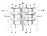
次に、FPC505が、複数の電子部品16が実装される電子部品実装領域を複数箇所有している場合における基板吸着用溝部の配置について、図36に示すFPC505の電子部品実装面505aの模式平面図を用いて説明する。
【0140】
図36に示すように、FPC505は、上記電子部品実装領域として、電子部品実装領域40a、40b、及び40cの3箇所の領域を有している。夫々の電子部品実装領域40a、40b、及び40cにおいては、複数の電子部品16が、互いに狭隣接されて装着されている。なお、本説明においては、夫々の電子部品実装領域40a、40b、及び40cにおいて、複数の電子部品16が装着されている場合について説明するが、上記電子部品実装領域に装着されている電子部品16の個数は複数に限定されるものではなく、1個のみの電子部品16が装着れているような場合であってもよい。また、装着されている夫々の電子部品16の種類についても、同じ種類に限定されるものではなく、異なる種類の電子部品16が同一の上記電子部品実装領域に装着されているような場合であってもよい。
【0141】
また、図36に示すように、電子部品実装領域40aを取り囲むように、かつ、電子部品実装領域40aの外周における各辺と平行かつ直線的に、図示しない載置部材の上面に、基板吸着用溝部41aが形成されており、同様に、電子部品実装領域40bを取り囲むように、基板吸着用溝部41bが形成されており、電子部品実装領域40cを取り囲むように、基板吸着用溝部41cが形成されている。また、夫々の基板吸着用溝部41a、41b、及び41cは、互いに基板吸着用溝部41により接続されている。
【0142】
このように夫々の基板吸着用溝部41a、41b、及び41cが配置形成されていることにより、FPC505における裏面(すなわち、載置部材接触面505b)における平面的に夫々の基板吸着用溝部41a、41b、及び41cに対応する夫々の領域を、吸着領域とすることができるとともに、夫々の吸着領域で囲まれた領域、すなわち、夫々の電子部品実装領域40a、40b、及び40cに対応する領域を、半田配置領域と見なすことができる。
【0143】
従って、夫々の基板吸着用溝部41a、41b、及び41cにより、夫々の吸着領域を吸着することにより、夫々の半田配置領域を、載置部材の上面に確実に接触されることができる。従って、載置部材よりFPC505における夫々の電子部品実装領域40a、40b、及び40cに確実かつ効率的に伝熱を行うことができ、より効率的な夫々の電子部品16の接合を行うことができる。
【0144】
なお、上記においては、夫々の電子部品実装領域40a、40b、及び40cを同時的に載置部材の表面に接触されて伝熱を行なう場合について説明したが、このような場合にのみ限定されるものではない。例えば、夫々の電子部品実装領域40a、40b、及び40cを取り囲むように形成されている夫々の基板吸着用溝部41a、41b、及び41cを、互いに接続させることなく、個別に吸着/吸着解除可能とするとともに、載置部材により、夫々の電子部品実装領域40a、40b、及び40cを個別に伝熱加熱可能とさせるような場合であってもよい。このような場合にあっては、夫々の電子部品実装領域40a、40b、及び40cを、個別に吸着することにより、個別に載置部材の表面に接触されて伝熱を行なうことができる。従って、特に、回路基板が、撓んだり、変形して曲げられたような場合に、夫々の電子部品実装領域40a、40b、及び40c毎に、個別に載置部材に接触させることができるため、より確実な伝熱を行なうことができ有効である。
【0145】
本発明は、添付図面を参照しながら好ましい実施形態に関連して充分に記載されているが、この技術の熟練した人々にとっては種々の変形や修正は明白である。そのような変形や修正は、添付した請求の範囲による本発明の範囲から外れない限りにおいて、その中に含まれると理解されるべきである。
【0146】
また、上記様々な実施形態のうちの任意の実施形態を適宜組み合わせることにより、それぞれの有する効果を奏するようにすることができる。
【0147】
【発明の効果】
本発明によれば、載置部材と加熱装置とを備え、一つの回路基板とほぼ同じ大きさにてなる載置部材に上記回路基板を接触させて上記加熱装置で加熱するようにしたことより、小型の回路基板に対してロスの発生を低減させることができ、かつ各種の回路基板に対応した加熱を個々に行うことができる。したがって、少量、多品種の回路基板について、従来に比べて高い生産性にて製造可能となる。
【0148】
又、上記回路基板を上記載置部材に吸着保持させる吸引装置を設けたことで、回路基板を載置部材に密着させることができ、回路基板の温度制御をより高い精度で行うことができる。
【0149】
さらに、上記吸引装置を直接接続する吸引用開口を上記載置部材に有することで、上記接合材料を溶融したとき該接合材料が上記加熱装置を汚すのを防止することができる。よって、加熱装置の清掃動作が不要となり、当該電子部品接合装置の稼動率を向上させることができる。
【0150】
上記載置部材が、さらに、当該載置部材に接触する上記回路基板の載置部材接触面における吸着領域を吸着し上記吸引用開口につながる基板吸着穴を備えていることにより、上記回路基板を上記載置部材に確実に密着させることができ、上記密着による伝熱加熱を確実かつ効率的に行なうことができる。
【0151】
密着用部材及び載置部材用吸引装置を備えることで、載置部材は、載置部材用吸引装置の吸引動作により加熱装置へ吸着保持させることができる。又、密着用部材を設けることで、上記吸着保持の際、加熱装置に対する載置部材の密着性を向上させることができる。
【0152】
密着用部材接触面及び密着用部材が吸着用空間を有することで、加熱装置に対する載置部材の吸着力を向上させることができる。
【0153】
上記回路基板の上記載置部材接触面において、上記電子部品装着面の上記接合材料の配置領域に対応する接合材料配置領域と、上記接合材料配置領域に隣接配置される上記吸着領域とが備えられ、上記載置部材は、その回路基板接触面において、上記接合材料配置領域に対応する伝熱部と、上記吸着領域に対応する上記基板吸着穴とを備えることにより、上記伝熱部と上記接合材料配置領域とを互いに接触させるように、上記基板吸着穴により上記吸着領域を吸着しながら、上記接触による上記伝達部より上記接合材配置領域への伝熱加熱を確実に行なうことができる。
【0154】
また、上記基板吸着穴と上記伝熱部とが隣接して配置されていることにより、上記基板吸着穴による吸着により、互いの確実な接触が要求される上記接合材料配置領域と上記伝熱部とを、より安定させて接触させることができる。
【0155】
これにより、上記回路基板に反りや曲がりが生じているような場合であっても、上記接合材料配置領域以外の領域の状態に拘らず、上記接合材料配置領域全体を確実に上記載置部材の上記伝熱部に接触させることができる。従って、上記電子部品の上記回路基板への接合を確実かつ効率的に行うことができる。
【0156】
上記基板吸着穴が、上記電子部品装着面への上記電子部品の投影された外形形状における少なくとも一辺に平行に延在するように、形成された溝状の穴であることにより、上記溝状の基板吸着穴の配置を上記電子部品の上記外形形状に関係付けることができるため、上記吸着をより確実かつ安定したものとすることができる。また、上記溝状の形状とされていることより、上記吸着領域を拡大させることができ、より安定した吸着を行なうことができる。
【0157】
本発明の別の態様によれば、上記回路基板が、1つの上記電子部品を上記回路基板に接合する互いに離間された2つの上記接合材料の上記配置領域を有し、上記載置部材接触面において、上記2つの配置領域に対応する夫々の上記接合材料配置領域と、上記夫々の接合材料配置領域の間に配置された上記吸着領域とを有するような場合であっても、上記載置部材において、上記夫々の接合材料配置領域に対応させた上記夫々の伝熱部と、上記吸着領域に対応させた上記基板吸着穴とを備えさせることにより、上記確実かつ安定した吸着を行なうことができるとともに、効率的な伝熱加熱を行なうことができる。
【0158】
又、上記回路基板が、複数の電子部品を整列配置させて備える場合や、1又は複数の電子部品が実装される複数の電子部品実装領域を備えるような場合であっても、上記電子部品の整列配置の方向や上記電子部品実装領域に関係させて、上記基板吸着用溝部や上記基板吸着穴を配置させることにより、上記確実かつ安定した吸着を行うことができ、効率的な伝熱加熱を行なうことができる。
【0159】
又、上記基板吸着穴が、上記吸引装置による吸引におけるその流速が、上記吸引用開口における流速よりも大きくなるように形成されていることにより、上記回路基板を吸着する位置での上記吸引の流速を高めることができるため、より確実に上記吸着を行なうことができる。
【0160】
又、厚みが0.02mmから1mmの範囲である回路基板や、フレキシブル基板にてなる回路基板では、上記加熱装置による加熱制御に対する基板の温度応答性が良いことから、各種の回路基板毎に、適切な温度制御にて加熱を行うことが可能となる。
【0161】
又、上記夫々の態様による効果を得ることができる電子部品接合装置を備える電子部品実装装置を提供することができ、又、上記夫々の態様による効果を得ることができる電子部品の回路基板への接合方法を提供することができる。
【図面の簡単な説明】
【図1】 本発明の第1実施形態における電子部品接合装置の構造の模式説明図である。
【図2】 図1に示す電子部品接合装置にて加熱されるのに好適な回路基板の斜視図である。
【図3】 図1に示す電子部品接合装置を構成する載置部材の斜視図である。
【図4】 図1に示す電子部品接合装置を構成する加熱装置の斜視図である。
【図5】 図1に示す電子部品接合装置にて実行される温度制御にて使用される温度プロファイルの一例を示すグラフである。
【図6】 図1に示す電子部品接合装置にて実行される温度制御にて使用される温度プロファイルの他の例を示すグラフである。
【図7】 図1に示す電子部品接合装置にて実行される温度制御にて使用される温度プロファイルのさらに別の例を示すグラフである。
【図8】 図1に示す電子部品接合装置の変形例を示す斜視図である。
【図9】 図1に示す電子部品接合装置の他の変形例を示す図である。
【図10】 図1に示す電子部品接合装置を利用して構成される加熱接合装置の斜視図である。
【図11】 図10に示す加熱接合装置を備えて構成される実装システムを示す斜視図である。
【図12】 図10に示す加熱接合装置を備えて構成される実装システムの他の例における斜視図である。
【図13】 図1に示す電子部品接合装置への回路基板の搬送装置の他の例を示す図である。
【図14】 図1に示す電子部品接合装置の他の実施形態を示す斜視図である。
【図15】 図14に示す載置部材の斜視図である。
【図16】 図14に示す電子部品接合装置の断面図である。
【図17】 図14に示す密着用部材の斜視図である。
【図18】 図14に示すヒータ部の斜視図である。
【図19】 従来の部品実装システムを示す斜視図である。
【図20】 従来のリフロー装置にてFPCの処理を行うとき、パレット上にFPCが配列された状態を示す図である。
【図21】 従来、回路基板内の局部領域のみを加熱する場合の装置構成を示す斜視図である。
【図22】 本発明の第4実施形態にかかる電子部品接合装置の部分断面模式図であり、(A)はFPCの部分断面模式図であり、(B)は載置部材の部分断面模式図である。
【図23】 上記第4実施形態における実施例を示す模式図であり、(A)〜(C)の夫々は、チップ部品と基板吸着用溝部との配置関係を示す模式平面図である。
【図24】 上記第4実施形態における実施例を示す模式図であり、(A)はチップ部品と基板吸着用溝部との配置関係を示す模式平面図であり、(B)は(A)におけるX−X断面の矢視断面図である。
【図25】 上記第4実施形態の実施例におけるチップ部品と基板吸着用溝部との配置関係を示す模式平面図である。
【図26】 上記第4実施形態の実施例におけるチップ部品と基板吸着用溝部との配置関係を示す模式平面図である。
【図27】 上記第4実施形態の実施例において、複数のチップ部品が整列配置されている場合におけるチップ部品と基板吸着用溝部との配置関係を示す模式平面図である。
【図28】 上記第4実施形態の実施例において、複数のチップ部品が複数列に整列配置されている場合におけるチップ部品と基板吸着用溝部との配置関係を示す模式平面図である。
【図29】 図28の場合における基板吸着用溝部のさらに別の配置を示す模式平面図である。
【図30】 図27の場合における基板吸着用溝部のさらに別の配置を示す模式平面図である。
【図31】 上記第4実施形態の実施例において、複数のチップ部品が整列配置されていない場合におけるチップ部品と基板吸着用溝部との配置関係を示す模式平面図である。
【図32】 QFPの構成を示す模式斜視図である。
【図33】 上記第4実施形態の実施例において、QFPと基板吸着用溝部との配置関係を示す模式平面図である。
【図34】 図33の場合における基板吸着用溝部のさらに別の配置を示す模式平面図である。
【図35】 上記第4実施形態の実施例において、(A)はFPC、基板吸着穴、及びベアICの配置関係を示す模式平面図であり、(B)はベアICの構成を示す模式斜視図である。
【図36】 上記第4実施形態の実施例において、複数の電子部品実装領域と基板吸着用溝部との配置関係を示す模式平面図である。
【符号の説明】
5…回路基板(FPC)、6…電子部品(チップ部品)、7…IC、8…半田、18…半田部、21…基板吸着用溝部、41…電子部品実装領域、101…電子部品接合装置、110…載置部材、120…加熱装置、121…ヒータ部、131…回路基板用吸引装置、141…ヒータ部用冷却装置、201…実装システム、230…加熱接合装置、250…実装システム、505…FPC、505a…電子部品実装面、505b…載置部材接触面、505d…吸着領域、505e…半田配置領域、510…載置部材、510a…回路基板載置面、510b…伝熱部、511…基板吸着穴。[0001]
BACKGROUND OF THE INVENTION
The present invention relates to an electronic component bonding apparatus and method for bonding an electronic component to a circuit board by a heating source, and an electronic component mounting apparatus including the electronic component bonding apparatus, and particularly, a small and thin type used for small mobile devices. The present invention relates to an electronic component bonding apparatus and method for manufacturing a circuit board, and an electronic component mounting apparatus.
[0002]
[Prior art]
Conventionally, in a liquid crystal module used for a mobile device or the like, an electronic component is mounted on a flexible substrate (FPC) in order to perform display control of a liquid crystal display unit and to electrically connect the liquid crystal module and the mother substrate. The FPC is mounted with the display control driver IC and chip components such as a capacitor. Since the connection portion of the driver IC has a narrow pitch, and contamination of the connection portion causes a decrease in the reliability of the liquid crystal module, the driver IC is usually mounted before mounting the chip component.
[0003]
After mounting the driver IC, as shown in FIG. 19, the
[0004]
In addition, when producing different types of FPC 5, each FPC 5 mounted with parts corresponding to each type is transported. In this case, the reflow apparatus for heating the furnace atmosphere is not productive and is necessary. It is more efficient to heat only the part. Therefore, a reflow apparatus using local heating by the light beam method as shown in FIG. 21 is effective. In particular, in order to prevent the light from being irradiated to a portion other than the necessary portion, it is effective to irradiate the light irradiated from the
[0005]
When producing the same kind of
[0006]
In addition, since the production equipment as shown in FIG. 19 is premised on processing a large substrate, the apparatus itself is large. Especially in a reflow apparatus that heats the atmosphere in the furnace, 3 to 5 m is required for soaking. The length is general, and when viewed from the size of a circuit board of about 2 to 30 mm, the equipment is too large and it is difficult to take flexible measures. In the system including the
[0007]
The above light beam method is effective in the case of the same component or a small number of components. However, as the functionality of the liquid crystal module increases, the number and types of
[0008]
On the other hand, instead of heating the atmosphere around the circuit board in order to cope with such a problem, the stage on which the circuit board is mounted is provided with a heating device, and the circuit board is heated through the stage. Thus, an apparatus has been devised that heats and melts solder (see, for example, Patent Document 1). In such an apparatus, since the circuit board is directly heated without heating the atmosphere around the circuit board, the energy required for heating from the apparatus is obtained by heating and melting the solder. It can be used efficiently.
[0009]
[Patent Document 1]
JP 2002-151553 A
[0010]
[Problems to be solved by the invention]
However, diversification of electronic components mounted on the circuit board and the circuit board is progressing more and more, especially in the circuit board that tends to be thinned, the circuit board itself is likely to be warped or bent, In the method of transferring heat to the circuit board through the stage, the contact between the stage and the circuit board may be insufficient, the heat transfer becomes insufficient, and the solder is heated and melted. There is a problem in that there may be cases where it cannot be performed reliably and efficiently.
[0011]
Accordingly, an object of the present invention is to solve the above-described problems, and an electronic component joining apparatus and method that can be manufactured with a higher productivity than conventional devices for a small amount and a variety of circuit boards, and the above-described electronic An object of the present invention is to provide an electronic component mounting apparatus including a component bonding apparatus.
[0012]
[Means for Solving the Problems]
In order to achieve the above object, the present invention is configured as follows.
[0015]
According to the first aspect of the present invention, the mounting member for mounting the circuit board on which the electronic component is mounted;
A heating device that heats the mounting member and heats the circuit board that is in contact with the mounting member to melt a bonding material that bonds the electronic component and the circuit board;
A circuit board suction device for adsorbing and holding the circuit board on the mounting member;
A mounting member suction device for adsorbing and holding the mounting member to the heating device,
The mounting member includes a substrate suction hole for sucking a suction region on the mounting member contact surface of the circuit board that contacts the mounting member, and the circuit board on the mounting member.For boardA circuit board suction passage for communicating with a suction opening directly connected to the suction device;
The heating device provides an electronic component bonding apparatus characterized in that the heating device is connected to the above-described suction member for a placement member and has a placement member suction passage for sucking the placement member.
[0016]
Of the present inventionSecond aspectA plurality of mounting members for mounting the circuit board on which the electronic component is mounted;
AboveThe mounting member is heated topluralA heating device that heats the circuit board in contact with the mounting member and melts a bonding material for bonding the electronic component and the circuit board;
UpCircuit board abovepluralAdsorb and hold on the mounting memberFor circuit boardWith suction device,
A mounting member suction device for adsorbing and holding the plurality of mounting members to the heating device;With
The mounting member described above isA substrate suction hole for sucking a suction region on the mounting member contact surface of the circuit board in contact with the mounting member;On the mounting memberFor circuit boardSuction opening for directly connecting a suction deviceA circuit board suction passage that communicates with
The heating device connects the heating device to the mounting member suction device described above, and has a mounting member suction passage for sucking the plurality of mounting members.There is provided an electronic component joining apparatus characterized by comprising:
[0018]
Of the present inventionThird aspectAccording to the present invention, the contact member that is sandwiched between the mounting member and the heating device and makes the mounting member and the heating device closely contact each otherTheFurther prepare1st aspect or 2nd aspectThe electronic component joining apparatus described in 1. is provided.
[0019]
Of the present inventionFourth aspectAccording to the above, the contact member contact surface of the placement member that contacts the contact member, and the contact member have a suction space that is sucked by the placement member suction device.Third aspectThe electronic component joining apparatus described in 1. is provided.
[0020]
Of the present invention5th aspectAccording to the above mounting member, in its circuit board contact surface,
A heat transfer section that conducts heat transfer by contact to the bonding material arrangement area on the placement member contact surface corresponding to the arrangement area of the bonding material on the electronic component mounting surface of the circuit board on which the electronic component is mounted;
The substrate adsorption for adsorbing the adsorption area arranged adjacent to the bonding material arrangement area on the placement member contact surface on the circuit board so as to bring the heat transfer section and the bonding material arrangement area into contact with each other. With holes1st aspect or 2nd aspectThe electronic component joining apparatus described in 1. is provided.
[0021]
Of the present inventionSixth aspectAccording to the present invention, the circuit board contact of the mounting member is such that the board suction hole extends parallel to at least one side of the outer shape of the electronic component projected onto the electronic component mounting surface of the circuit board. It is a groove-shaped hole formed on the surface5th aspectThe electronic component joining apparatus described in 1. is provided.
[0022]
Of the present invention7th aspectAccording to the above-mentioned mounting member,
Each said joining material in the said mounting member contact surface corresponding to the said arrangement | positioning area | region of the two said joining materials spaced apart from each other which joins said one electronic component in said electronic component mounting surface of said circuit board to said circuit board An arrangement region and the corresponding heat transfer section;
The suction area disposed between the respective bonding material arrangement areas on the placement member contact surface on the circuit board, and the corresponding board suction hole.5th aspect or 6th aspectThe electronic component joining apparatus described in 1. is provided.
[0023]
Of the present inventionEighth aspectAccording to the present invention, the board suction hole is formed in a groove-like shape formed on the circuit board contact surface of the mounting member in parallel with the direction of the arrangement of the circuit board on which the plurality of electronic components are arranged. Is a hole5th to 7th aspectsAn electronic component joining apparatus according to any one of the above is provided.
[0024]
Of the present inventionNinth aspectAccording to the above, the mounting member is the circuit board contact surface,
To a plurality of bonding material arrangement regions on the placement member contact surface corresponding to a plurality of electronic component mounting regions on which one or more electronic components are mounted on the electronic component mounting surface of the circuit board on which the electronic components are mounted A plurality of heat transfer parts that perform heat transfer by contact;
A plurality of the adsorption regions arranged adjacent to the respective bonding material arrangement regions on the placement member contact surface on the circuit board, the respective heat transfer portions and the respective bonding material arrangement regions are mutually connected. A plurality of the substrate suction holes to be sucked so as to be brought into contact with each other1st aspect or 2nd aspectThe electronic component joining apparatus described in 1. is provided.
[0025]
Of the present inventionTenth aspectAccording to the present invention, the substrate suction hole is formed such that the flow rate in the suction by the suction device is larger than the flow rate in the suction opening.1st to 9th aspectsAn electronic component joining apparatus according to any one of the above is provided.
[0026]
Of the present inventionEleventh aspectAccording to the first aspect, the circuit board has a thickness in the range of 0.02 mm to 1 mm.Tenth aspectAn electronic component joining apparatus according to any one of the above is provided.
[0027]
Of the present invention12th aspectAccording to the above, the circuit board is a flexible board1st aspect to 11th aspectAn electronic component joining apparatus according to any one of the above is provided.
[0028]
Of the present invention13th aspectAccording to the electronic component mounting apparatus for mounting the electronic component on the circuit board via the bonding material,
From the first aspect12th aspectAn electronic component mounting apparatus comprising the electronic component bonding apparatus according to any one of the above.
[0029]
Of the present invention14th aspectAccording to the above, the circuit board on which the electronic component to be bonded with the bonding material is mounted is mounted on the mounting member,
Adjacent to the bonding material arrangement region on the mounting member contact surface of the circuit board that contacts the mounting member, corresponding to the arrangement region of the bonding material on the electronic component mounting surface of the circuit board on which the electronic component is mounted. The suction areaThe suction through the circuit board suction passage by the circuit board suction device directly connected to the circuit board suction passage in the mounting memberAdsorb to bring the bonding material arrangement area into contact with the mounting member.In addition, while the above-described mounting member is sucked and held by the heating device by suction through the mounting member suction passage by the mounting member suction device connected to the mounting member suction passage in the heating device, Via the mounting member by the above heating deviceThere is provided an electronic component bonding method characterized by heating the circuit board in the bonding material arrangement region, melting the bonding material, and bonding the electronic component to the circuit board.
[0030]
DETAILED DESCRIPTION OF THE INVENTION
Hereinafter, an electronic component bonding apparatus, an electronic component bonding method, a circuit board, and an electronic component mounting apparatus, which are embodiments of the present invention, will be described with reference to the drawings. Here, the electronic component bonding method is a method executed by the electronic component bonding apparatus, the circuit board is a substrate bonded with electronic components by the electronic component bonding method, and the electronic component mounting apparatus is It is an apparatus provided with the said electronic component joining apparatus. Moreover, the same code | symbol is attached | subjected about the same component in each figure.
[0031]
In the following embodiments, the electronic component is a component that is surface-mounted on a circuit board and bonded to the circuit board by a bonding material, and corresponds to, for example, a
[0032]
(First embodiment)
1 to 4 show an electronic
[0033]
The electronic
[0034]
The mounting
[0035]
Further, as shown in FIG. 3, a
[0036]
The
[0037]
The
[0038]
The temperature of the
[0039]
The
[0040]
A circuit
[0041]
Further, a heater
[0042]
The circuit
[0043]
As the temperature profile, for example, forms shown in FIGS. 5 to 7 are conceivable. For example, the type of bonding material, the type and number of electronic components bonded on the circuit board, the material and thickness of the circuit board, etc. An optimum temperature profile is selected according to each parameter. As a selection method, various temperature profiles corresponding to the above parameters are stored in the
[0044]
5 to 7, as an example, a0 is room temperature, a1 is the melting point of the bonding material, and in this embodiment, the bonding material is eutectic solder, so 183 ° C, a2 is 230 ° C, and b1 is 150 ° C., b2 is 220 ° C., t1 is 1 second, t2 is 3 seconds, t3 is 4 seconds, t4 is 10 seconds, and t5 is 6 seconds.
[0045]
In particular, when the
[0046]
Further, when it is necessary to suppress the generation of solder balls at the time of melting the solder, it is preferable to provide a preheating operation for maintaining the same temperature from time t1 to time t2, as shown in FIG. On the other hand, when the electronic component is relatively large and the influence of the solder ball is negligible, as shown in FIG. 6, the preheating operation may not be provided and the solder may be melted at once. Further, when it is desired to shorten the time required for melting the solder and joining the electronic component to the circuit board, as shown in FIG. 7, the temperature b1 is started from the preheating temperature b1 in advance and the temperature b1 is set after the soldering is finished. A method of maintaining is also possible.
[0047]
Regarding the electronic
[0048]
First, the mounting
[0049]
According to the electronic
[0050]
Specifically, in the conventional reflow furnace, about 20 kW is required as a unit energy per a predetermined number of circuit boards required for the heating, whereas in the electronic
[0051]
Further, since the circuit board is brought into contact with the mounting
[0052]
In the electronic
[0053]
With this configuration, the electronic
[0054]
In addition, by adopting the above-mentioned parallel structure, one heating control can be performed over the entire heating area of one circuit board, and at a plurality of locations in the heating area of one circuit board. It is also possible to perform different heating controls, and the versatility can be further improved.
[0055]
Furthermore, when it is necessary to change the heating conditions of the circuit board more locally, a light beam, a laser, hot air, or the like is applied from above the
[0056]
(Second Embodiment)
Next, an electronic component mounting apparatus (also referred to as “mounting system”) configured using the electronic
[0057]
The mounting
[0058]
As described in the description of the electronic
[0059]
The
[0060]
The
[0061]
The carry-in
[0062]
The
[0063]
In FIG. 10, the
[0064]
The
[0065]
Further, the
[0066]
The operation in the mounting
[0067]
The
[0068]
Next, the
[0069]
The
[0070]
According to the mounting
[0071]
As shown in FIG. 11, the mounting
[0072]
The mounting
[0073]
The mounting
[0074]
The circuit board is placed on the working
[0075]
For example, when the first circuit board is heated by the
[0076]
By adopting a configuration including the rotary table 257 as in the mounting
[0077]
Further, when the stop position of the rotary table 257 is divided into eight parts, between the
[0078]
In each of the embodiments described above, the
[0079]
(Third embodiment)
As described above, in the electronic
[0080]
When the fumes flow into the
[0081]
Therefore, the electronic component bonding apparatus according to the third embodiment described below is an improved type of the electronic
[0082]
A flexible substrate (FPC) 405 shown in FIG. 14 is a substrate for connecting a liquid crystal module and a mother substrate, for example, as with the above-described
[0083]
As shown in FIG. 14, an electronic
[0084]
A mounting
[0085]
Furthermore, a plurality of substrate suction holes 411 for sucking and holding the
[0086]
Further, each
[0087]
Further, since the through-hole through
[0088]
Furthermore, on the contact
[0089]
As shown in FIG. 17, the
[0090]
By providing such a
[0091]
The
[0092]
In addition, the mounting
[0093]
The temperature of the
[0094]
The
[0095]
Regarding the electronic
[0096]
First, the
[0097]
The heating operation by the
[0098]
At this time, the fumes generated from the
[0099]
After the joining of the
[0100]
As in the case of the electronic
[0101]
(Fourth embodiment)
Next, an example of an electronic component bonding apparatus according to the fourth embodiment of the present invention will be described. The electronic component bonding apparatus according to the fourth embodiment has the same basic configuration as the electronic
[0102]
FIG. 22 is a diagram showing the relationship between the mounting
[0103]
As shown in FIG. 22A, the
[0104]
Further, as shown in FIG. 22B, when the
[0105]
As described above, the placement
[0106]
Further, since each of the
[0107]
Next, specific examples of the arrangement of the substrate suction holes 511 using the characteristics of the arrangement relationship between the
[0108]
First, FIGS. 23A to 23C are schematic plan views showing the arrangement relationship between the electronic component and the board suction hole as viewed from the electronic
[0109]
As shown in FIG. 23A, the
[0110]
On the other hand, the circuit
[0111]
As shown in FIG. 23A, the
[0112]
As described above, the
[0113]
Next, FIGS. 23B and 23C show an example in which the
[0114]
Next, FIG. 24A shows a schematic plan view showing the positional relationship between the
[0115]
As shown in FIG. 24A, the
[0116]
In addition, since the
[0117]
In FIG. 24, the increase in the suction flow rate is accommodated by increasing the formation depth without changing the formation width of the
[0118]
In the above description, it has been described that the flow rate in the suction of the
[0119]
Next, the arrangement of the
[0120]
As shown in FIG. 27, in the case where a plurality of
[0121]
In such a case, as shown in FIG. 27, each
[0122]
Furthermore, as shown in FIG. 28, in the case where the
[0123]
Alternatively, as shown in FIG. 29, two
[0124]
In either case of FIG. 28 and FIG. 29, the region where each
[0125]
Further, as shown in FIG. 30, the
[0126]
Such arrangement of the
[0127]
Further, as shown in FIG. 31, even if the
[0128]
Next, the arrangement of the substrate suction grooves when the
[0129]
FIG. 32 is a schematic perspective view showing a schematic structure of the
[0130]
As shown in FIG. 33, on the electronic
[0131]
Further, in FIG. 33, the case where the
[0132]
In addition, in the case where the size of the
[0133]
Next, as an example of the electronic component, the arrangement of the substrate suction holes in the case where the
[0134]
FIG. 35B is a perspective view showing a schematic structure of the
[0135]
As shown in FIG. 35B, the
[0136]
Further, as shown in FIG. 35B, since the
[0137]
As shown in FIG. 35A, the
[0138]
The same operation as described above is repeated for the other
[0139]
Next, with respect to the arrangement of the groove portions for substrate adsorption when the
[0140]
As shown in FIG. 36, the
[0141]
Further, as shown in FIG. 36, the substrate adsorbing area is arranged on the upper surface of a mounting member (not shown) so as to surround the electronic
[0142]
Since the respective
[0143]
Therefore, by adsorbing the respective adsorption regions by the respective
[0144]
In the above description, the case where the respective electronic
[0145]
Although the present invention has been fully described in connection with preferred embodiments with reference to the accompanying drawings, various variations and modifications will be apparent to those skilled in the art. Such changes and modifications are to be understood as being included therein, so long as they do not depart from the scope of the present invention according to the appended claims.
[0146]
In addition, by appropriately combining arbitrary embodiments of the various embodiments described above, it is possible to achieve the respective effects.
[0147]
【The invention's effect】
According to the present invention,A mounting member and a heating device are provided, and the circuit board is brought into contact with a mounting member that is approximately the same size as one circuit board and heated by the heating device. On the other hand, the generation of loss can be reduced, and heating corresponding to various circuit boards can be performed individually. Therefore, it is possible to manufacture a small amount and a wide variety of circuit boards with higher productivity than conventional ones.
[0148]
Further, by providing the suction device for adsorbing and holding the circuit board to the mounting member, the circuit board can be brought into close contact with the mounting member, and the temperature control of the circuit board can be performed with higher accuracy.
[0149]
further,By having the suction opening for directly connecting the suction device in the mounting member, it is possible to prevent the joining material from contaminating the heating device when the joining material is melted. Therefore, the cleaning operation of the heating device becomes unnecessary, and the operating rate of the electronic component joining device can be improved.
[0150]
UpThe mounting member further includes a substrate suction hole that sucks a suction region on the mounting member contact surface of the circuit board that contacts the mounting member and leads to the suction opening, thereby raising the circuit board. The contact member can be reliably brought into close contact, and heat transfer heating by the close contact can be reliably and efficiently performed.
[0151]
DenseBy providing the wearing member and the mounting member suction device, the mounting member can be sucked and held by the heating device by the suction operation of the mounting member suction device. In addition, by providing the adhesion member, the adhesion of the mounting member to the heating device can be improved during the adsorption holding.
[0152]
DenseSince the wearing member contact surface and the contact member have the space for suction, the suction force of the mounting member with respect to the heating device can be improved.
[0153]
UpThe mounting member contact surface on the circuit board includes a bonding material arrangement region corresponding to the bonding material arrangement region on the electronic component mounting surface, and the adsorption region arranged adjacent to the bonding material arrangement region. The mounting member includes, on the circuit board contact surface, the heat transfer portion corresponding to the bonding material arrangement region and the substrate suction hole corresponding to the suction region, whereby the heat transfer portion and the bonding member are provided. Heat transfer heating from the transmission part to the bonding material arrangement region by the contact can be performed reliably while adsorbing the adsorption region by the substrate adsorption hole so as to bring the material arrangement region into contact with each other.
[0154]
In addition, since the substrate suction hole and the heat transfer portion are arranged adjacent to each other, the bonding material placement region and the heat transfer portion that require reliable contact with each other due to suction by the substrate suction hole. Can be brought into contact with more stability.
[0155]
Thus, even when the circuit board is warped or bent, the entire bonding material arrangement region can be securely attached to the mounting member regardless of the state of the region other than the bonding material arrangement region. The heat transfer part can be contacted. Therefore, the electronic component can be reliably and efficiently joined to the circuit board.
[0156]
UpThe substrate suction hole is a groove-shaped hole formed so as to extend in parallel with at least one side of the outer shape projected of the electronic component on the electronic component mounting surface. Since the arrangement of the substrate suction holes can be related to the outer shape of the electronic component, the suction can be made more reliable and stable. Moreover, since it is set as the said groove shape, the said adsorption | suction area | region can be expanded and more stable adsorption | suction can be performed.
[0157]
According to another aspect of the present invention, the circuit board has the placement region of the two joining materials spaced apart from each other for joining one electronic component to the circuit board, and the placement member contact surface described above In the above, even in the case of having each of the bonding material arrangement areas corresponding to the two arrangement areas and the adsorption area arranged between the respective bonding material arrangement areas, In this case, the reliable and stable adsorption can be performed by providing the respective heat transfer portions corresponding to the respective bonding material arrangement regions and the substrate adsorption holes corresponding to the adsorption regions. At the same time, efficient heat transfer heating can be performed.
[0158]
In addition, even when the circuit board includes a plurality of electronic components arranged in an aligned manner or a plurality of electronic component mounting regions on which one or a plurality of electronic components are mounted, By placing the substrate suction groove and the substrate suction hole in relation to the direction of alignment and the electronic component mounting area, the reliable and stable suction can be performed, and efficient heat transfer heating can be performed. Can be done.
[0159]
Further, since the substrate suction hole is formed so that the flow rate in the suction by the suction device is larger than the flow rate in the suction opening, the suction flow rate at the position for sucking the circuit board. Therefore, the adsorption can be performed more reliably.
[0160]
In addition, in a circuit board having a thickness in the range of 0.02 mm to 1 mm and a circuit board made of a flexible board, the temperature responsiveness of the board to the heating control by the heating device is good. Heating can be performed with appropriate temperature control.
[0161]
In addition, an electronic component mounting apparatus including an electronic component bonding apparatus that can obtain the effects of the above aspects can be provided, and the electronic component that can obtain the effects of the above aspects can be applied to a circuit board. A bonding method can be provided.
[Brief description of the drawings]
FIG. 1 is a schematic explanatory diagram of the structure of an electronic component bonding apparatus according to a first embodiment of the present invention.
FIG. 2 is a perspective view of a circuit board suitable for being heated by the electronic component bonding apparatus shown in FIG.
3 is a perspective view of a mounting member constituting the electronic component bonding apparatus shown in FIG.
4 is a perspective view of a heating device constituting the electronic component bonding apparatus shown in FIG.
FIG. 5 is a graph showing an example of a temperature profile used in temperature control executed by the electronic component bonding apparatus shown in FIG. 1;
6 is a graph showing another example of a temperature profile used in temperature control executed in the electronic component bonding apparatus shown in FIG.
FIG. 7 is a graph showing still another example of a temperature profile used in temperature control executed in the electronic component bonding apparatus shown in FIG. 1;
FIG. 8 is a perspective view showing a modified example of the electronic component bonding apparatus shown in FIG.
FIG. 9 is a view showing another modification of the electronic component bonding apparatus shown in FIG. 1;
FIG. 10 is a perspective view of a heat bonding apparatus configured using the electronic component bonding apparatus shown in FIG.
11 is a perspective view showing a mounting system including the heat bonding apparatus shown in FIG.
12 is a perspective view of another example of a mounting system including the heat bonding apparatus shown in FIG.
13 is a view showing another example of a circuit board transfer device to the electronic component bonding apparatus shown in FIG. 1; FIG.
FIG. 14 is a perspective view showing another embodiment of the electronic component bonding apparatus shown in FIG. 1;
15 is a perspective view of the mounting member shown in FIG.
16 is a cross-sectional view of the electronic component bonding apparatus shown in FIG.
17 is a perspective view of the contact member shown in FIG. 14. FIG.
18 is a perspective view of the heater portion shown in FIG.
FIG. 19 is a perspective view showing a conventional component mounting system.
FIG. 20 is a diagram showing a state in which FPCs are arranged on a pallet when FPC processing is performed by a conventional reflow apparatus.
FIG. 21 is a perspective view showing an apparatus configuration in the case where only a local area in a circuit board is conventionally heated.
FIG. 22 is a partial cross-sectional schematic view of an electronic component bonding apparatus according to a fourth embodiment of the present invention, (A) is a partial cross-sectional schematic view of an FPC, and (B) is a partial cross-sectional schematic view of a mounting member. It is.
FIG. 23 is a schematic diagram showing an example in the fourth embodiment, and each of (A) to (C) is a schematic plan view showing an arrangement relationship between a chip component and a substrate suction groove.
24 is a schematic view showing an example of the fourth embodiment, FIG. 24 (A) is a schematic plan view showing an arrangement relationship between a chip component and a substrate suction groove, and FIG. 24 (B) is a schematic view of FIG. It is arrow sectional drawing of a XX cross section.
FIG. 25 is a schematic plan view showing the positional relationship between chip components and substrate suction grooves in the example of the fourth embodiment.
FIG. 26 is a schematic plan view showing the positional relationship between chip components and substrate suction grooves in the example of the fourth embodiment.
FIG. 27 is a schematic plan view showing an arrangement relationship between chip components and substrate suction grooves when a plurality of chip components are arranged in alignment in the example of the fourth embodiment.
FIG. 28 is a schematic plan view showing an arrangement relationship between chip components and substrate suction grooves when a plurality of chip components are arranged in a plurality of rows in the example of the fourth embodiment.
FIG. 29 is a schematic plan view showing still another arrangement of the substrate adsorption groove in the case of FIG.
30 is a schematic plan view showing still another arrangement of the substrate adsorption groove in the case of FIG. 27. FIG.
FIG. 31 is a schematic plan view showing the positional relationship between chip components and substrate suction grooves when a plurality of chip components are not aligned in the example of the fourth embodiment.
FIG. 32 is a schematic perspective view showing a configuration of a QFP.
FIG. 33 is a schematic plan view showing the positional relationship between the QFP and the substrate suction groove in the example of the fourth embodiment.
34 is a schematic plan view showing still another arrangement of the substrate suction groove portions in the case of FIG. 33. FIG.
FIG. 35A is a schematic plan view showing the positional relationship between an FPC, a substrate suction hole, and a bare IC in the example of the fourth embodiment, and FIG. 35B is a schematic perspective view showing the configuration of the bare IC. FIG.
FIG. 36 is a schematic plan view showing an arrangement relationship between a plurality of electronic component mounting areas and substrate suction grooves in the example of the fourth embodiment.
[Explanation of symbols]
DESCRIPTION OF
Claims (14)
上記載置部材を加熱して上記載置部材に接触している上記回路基板を加熱し上記電子部品と上記回路基板とを接合する接合材料を溶融させる加熱装置と、
上記回路基板を上記載置部材に吸着保持させる回路基板用吸引装置と、
上記載置部材を上記加熱装置に吸着保持させる載置部材用吸引装置とを備え、
上記載置部材は、当該載置部材に接触する上記回路基板の載置部材接触面における吸着領域を吸着する基板吸着穴と、当該載置部材に上記回路基板用吸引装置を直接接続する吸引用開口とを連通させる回路基板吸引用通路を有し、
上記加熱装置は、当該加熱装置を上記載置部材用吸引装置に接続し、上記載置部材を吸着する載置部材吸引用通路を有することを特徴とする電子部品接合装置。A mounting member for mounting a circuit board on which electronic components are mounted;
A heating device that heats the mounting member and heats the circuit board that is in contact with the mounting member to melt a bonding material that bonds the electronic component and the circuit board;
A circuit board suction device for adsorbing and holding the circuit board on the mounting member;
A mounting member suction device for adsorbing and holding the mounting member to the heating device,
The loading portion member is connected to the substrate suction holes for sucking the suction region of the mounting member contact surface of the circuit board in contact with the mounting member, the circuit board for the suction device to the mounting member directly sucked A circuit board suction passage for communicating with the opening for use,
The electronic device joining apparatus according to claim 1, wherein the heating device has a placement member suction passage for connecting the heating device to the placement member suction device and sucking the placement member.
上記複数の載置部材を加熱して上記複数の載置部材に接触している上記回路基板を加熱し上記電子部品と上記回路基板とを接合する接合材料を溶融させる加熱装置と、
上記回路基板を上記複数の載置部材に吸着保持させる回路基板用吸引装置と、
上記複数の載置部材を上記加熱装置に吸着保持させる載置部材用吸引装置とを備え、
上記載置部材は、当該載置部材に接触する上記回路基板の載置部材接触面における吸着領域を吸着する基板吸着穴と、当該載置部材に上記回路基板用吸引装置を直接接続する吸引用開口とを連通させる回路基板吸引用通路を有し、
上記加熱装置は、当該加熱装置を上記載置部材用吸引装置に接続し、上記複数の載置部材を吸着する載置部材吸引用通路を有することを特徴とする電子部品接合装置。A plurality of mounting members for mounting a circuit board on which electronic components are mounted;
A heating device that heats the plurality of placement members to heat the circuit board that is in contact with the plurality of placement members and melts a bonding material that joins the electronic component and the circuit board;
A circuit board suction device for adsorbing and holding the circuit board on the plurality of mounting members;
A mounting member suction device for adsorbing and holding the plurality of mounting members to the heating device;
The mounting member includes a substrate suction hole that sucks a suction region on the mounting member contact surface of the circuit board that contacts the mounting member, and a suction member that directly connects the circuit board suction device to the mounting member. A circuit board suction passage for communicating with the opening;
The electronic device joining apparatus according to claim 1, wherein the heating device includes a placement member suction passage for connecting the heating device to the placement member suction device and sucking the plurality of placement members.
上記電子部品が装着された上記回路基板の電子部品装着面における上記接合材料の配置領域に対応する上記載置部材接触面における接合材料配置領域への、接触による伝熱を行う伝熱部と、
上記回路基板の上記載置部材接触面における上記接合材料配置領域に隣接されて配置される上記吸着領域を、上記伝熱部と上記接合材料配置領域とを互いに接触させるように吸着する上記基板吸着穴とを備える請求項1又は2に記載の電子部品接合装置。The mounting member is a circuit board contact surface,
A heat transfer section that conducts heat transfer by contact to the bonding material arrangement area on the placement member contact surface corresponding to the arrangement area of the bonding material on the electronic component mounting surface of the circuit board on which the electronic component is mounted;
The said board | substrate adsorption | suction which adsorb | sucks the said adsorption | suction area | region arrange | positioned adjacent to the said bonding material arrangement | positioning area | region in the said mounting member contact surface on the said circuit board so that the said heat-transfer part and the said bonding | jointing material arrangement | positioning area may mutually contact. The electronic component joining apparatus according to claim 1, further comprising a hole.
上記回路基板の上記電子部品装着面における1つの上記電子部品を上記回路基板に接合する互いに離間された2つの上記接合材料の上記配置領域に対応する上記載置部材接触面における夫々の上記接合材料配置領域と、対応された上記伝熱部と、
上記回路基板の上記載置部材接触面における上記夫々の接合材料配置領域の間に配置された上記吸着領域と、対応された上記基板吸着穴とを備える請求項5又は6に記載の電子部品接合装置。The mounting member described above is
Each said joining material in the said mounting member contact surface corresponding to the said arrangement | positioning area | region of the two said joining materials spaced apart from each other which joins said one electronic component in said electronic component mounting surface of said circuit board to said circuit board An arrangement region and the corresponding heat transfer section;
The electronic component bonding according to claim 5 or 6, comprising the suction region disposed between the respective bonding material placement regions on the placement member contact surface on the circuit board, and the corresponding substrate suction hole. apparatus.
上記電子部品が装着された上記回路基板の電子部品装着面における1又は複数の上記電子部品が実装される複数の電子部品実装領域に対応する上記載置部材接触面における複数の接合材料配置領域への、接触による伝熱を行なう複数の伝熱部と、
上記回路基板の上記載置部材接触面における上記夫々の接合材料配置領域に隣接されて配置される複数の上記吸着領域を、上記夫々の伝熱部と上記夫々の上記接合材料配置領域とを互いに接触させるように、吸着する複数の上記基板吸着穴とを備える請求項1又は2に記載の電子部品接合装置。In the above circuit board contact surface, the placing member is
To a plurality of bonding material arrangement regions on the placement member contact surface corresponding to a plurality of electronic component mounting regions on which one or more electronic components are mounted on the electronic component mounting surface of the circuit board on which the electronic components are mounted A plurality of heat transfer parts that perform heat transfer by contact;
A plurality of the adsorption regions arranged adjacent to the respective bonding material arrangement regions on the placement member contact surface on the circuit board, the respective heat transfer portions and the respective bonding material arrangement regions are mutually connected. The electronic component bonding apparatus according to claim 1, further comprising a plurality of the substrate suction holes to be sucked so as to be brought into contact with each other.
請求項1から12のいずれか1つに記載の電子部品接合装置とを備えることを特徴とする電子部品実装装置。An electronic component mounting apparatus for mounting the electronic component on the circuit board via the bonding material;
An electronic component mounting apparatus comprising: the electronic component bonding apparatus according to claim 1.
上記電子部品が装着された上記回路基板の電子部品装着面における上記接合材料の配置領域に対応する、上記載置部材に接触する上記回路基板の載置部材接触面における接合材料配置領域に隣接されて配置された吸着領域を、上記載置部材中の回路基板吸引用通路と直接接続された回路基板用吸引装置による上記回路基板吸引用通路を通しての吸引により吸着して、上記接合材料配置領域を上記載置部材に接触させるとともに、上記加熱装置中の載置部材吸引用通路と接続された載置部材用吸引装置による上記載置部材吸引用通路を通しての吸引により上記載置部材を上記加熱装置に吸着保持させながら、上記加熱装置により上記載置部材を介して上記接合材料配置領域における上記回路基板の加熱を行い、上記接合材料を溶融させて、上記電子部品を上記回路基板に接合させることを特徴とする電子部品接合方法。A circuit board on which electronic components to be bonded with a bonding material are mounted is mounted on a mounting member,
Adjacent to the bonding material arrangement area on the mounting member contact surface of the circuit board that contacts the mounting member, corresponding to the arrangement area of the bonding material on the electronic component mounting surface of the circuit board on which the electronic component is mounted. The adsorbing region arranged in the above-described manner is adsorbed by suction through the circuit board suction passage by the circuit board suction device directly connected to the circuit board suction passage in the placement member, and the bonding material placement region is The above-mentioned mounting member is brought into contact with the above-mentioned mounting member, and the above-mentioned mounting member is sucked through the above-described mounting member suction passage by the mounting member suction device connected to the mounting member suction passage in the above heating device. While adsorbing and holding, the heating device heats the circuit board in the bonding material arrangement region through the mounting member, melts the bonding material, and Electronic component bonding method characterized by bonding the child part on the circuit board.
Applications Claiming Priority (1)
| Application Number | Priority Date | Filing Date | Title |
|---|---|---|---|
| US10/244,429 US6797926B2 (en) | 2001-09-21 | 2002-09-17 | Apparatus and method for bonding electronic component, circuit board, and electronic component mounting apparatus |
Publications (2)
| Publication Number | Publication Date |
|---|---|
| JP2004111901A JP2004111901A (en) | 2004-04-08 |
| JP4130140B2 true JP4130140B2 (en) | 2008-08-06 |
Family
ID=32296788
Family Applications (1)
| Application Number | Title | Priority Date | Filing Date |
|---|---|---|---|
| JP2003076069A Expired - Fee Related JP4130140B2 (en) | 2002-09-17 | 2003-03-19 | Electronic component joining apparatus and method, and electronic component mounting apparatus |
Country Status (1)
| Country | Link |
|---|---|
| JP (1) | JP4130140B2 (en) |
Families Citing this family (4)
| Publication number | Priority date | Publication date | Assignee | Title |
|---|---|---|---|---|
| JP4621595B2 (en) * | 2006-01-11 | 2011-01-26 | 株式会社東芝 | Manufacturing method of semiconductor device |
| JP2007250704A (en) * | 2006-03-15 | 2007-09-27 | Nippon Avionics Co Ltd | Soldering device and method of soldering area array type part using the same, and method of removing the area array type part |
| JP2009212431A (en) * | 2008-03-06 | 2009-09-17 | Seiko Epson Corp | Reflow device and method of manufacturing semiconductor device |
| JP5343988B2 (en) | 2011-01-31 | 2013-11-13 | 株式会社デンソー | Brazing equipment |
-
2003
- 2003-03-19 JP JP2003076069A patent/JP4130140B2/en not_active Expired - Fee Related
Also Published As
| Publication number | Publication date |
|---|---|
| JP2004111901A (en) | 2004-04-08 |
Similar Documents
| Publication | Publication Date | Title |
|---|---|---|
| JP4371619B2 (en) | Reflow device | |
| US7357288B2 (en) | Component connecting apparatus | |
| JP3855879B2 (en) | Carrier for conveying flexible printed circuit board and method for mounting electronic component on flexible printed circuit board | |
| JP4793187B2 (en) | Electronic component mounting system and electronic component mounting method | |
| JP4190611B2 (en) | Component mounting method and component mounting apparatus | |
| KR100919931B1 (en) | Apparatus and Method for laser soldering and Fabricating method of power semiconductor module using the same | |
| JP4130140B2 (en) | Electronic component joining apparatus and method, and electronic component mounting apparatus | |
| JP2012129300A (en) | Mounting device and mounting method of electronic component | |
| JP3981259B2 (en) | Substrate support jig | |
| JP5662855B2 (en) | Printed circuit board manufacturing apparatus and manufacturing method | |
| JP2007059652A (en) | Electronic component mounting method | |
| JP4769697B2 (en) | Printed circuit board manufacturing method, printed circuit board assembly manufacturing method, and printed circuit board warpage correction method | |
| US5462626A (en) | Method of bonding an external lead and a tool therefor | |
| JP2005223241A (en) | Apparatus and method for bonding electronic component, and apparatus for mounting the electronic component | |
| US20060273138A1 (en) | Soldering apparatus for printed circuit board, soldering method for printed circuit board and soldering cream printing unit for soldering printed circuit board | |
| JP3907005B2 (en) | Circuit board manufacturing apparatus and method | |
| JPH0964521A (en) | Solder feeder and feeding method | |
| JP4702237B2 (en) | Electronic component mounting apparatus and electronic component mounting method | |
| JP4743059B2 (en) | Electronic component mounting system and electronic component mounting method | |
| JP3902037B2 (en) | Manufacturing method of semiconductor device | |
| JPH08139096A (en) | Electronic component, mounting of electronic component and electronic component mounting device | |
| KR100573248B1 (en) | Chip on film bonding system | |
| JPH0992971A (en) | Method and apparatus for connecting multikind conformable circuit board | |
| JP2023015448A (en) | Electronic component assembling apparatus and electronic component structure manufacturing apparatus | |
| JP2001028381A (en) | Packaging method and device thereof |
Legal Events
| Date | Code | Title | Description |
|---|---|---|---|
| A621 | Written request for application examination |
Free format text: JAPANESE INTERMEDIATE CODE: A621 Effective date: 20051027 |
|
| A977 | Report on retrieval |
Free format text: JAPANESE INTERMEDIATE CODE: A971007 Effective date: 20071121 |
|
| A131 | Notification of reasons for refusal |
Free format text: JAPANESE INTERMEDIATE CODE: A131 Effective date: 20071211 |
|
| A521 | Written amendment |
Free format text: JAPANESE INTERMEDIATE CODE: A523 Effective date: 20080121 |
|
| A131 | Notification of reasons for refusal |
Free format text: JAPANESE INTERMEDIATE CODE: A131 Effective date: 20080219 |
|
| A521 | Written amendment |
Free format text: JAPANESE INTERMEDIATE CODE: A523 Effective date: 20080328 |
|
| TRDD | Decision of grant or rejection written | ||
| A01 | Written decision to grant a patent or to grant a registration (utility model) |
Free format text: JAPANESE INTERMEDIATE CODE: A01 Effective date: 20080422 |
|
| A01 | Written decision to grant a patent or to grant a registration (utility model) |
Free format text: JAPANESE INTERMEDIATE CODE: A01 |
|
| A61 | First payment of annual fees (during grant procedure) |
Free format text: JAPANESE INTERMEDIATE CODE: A61 Effective date: 20080520 |
|
| R150 | Certificate of patent or registration of utility model |
Free format text: JAPANESE INTERMEDIATE CODE: R150 |
|
| FPAY | Renewal fee payment (event date is renewal date of database) |
Free format text: PAYMENT UNTIL: 20110530 Year of fee payment: 3 |
|
| FPAY | Renewal fee payment (event date is renewal date of database) |
Free format text: PAYMENT UNTIL: 20110530 Year of fee payment: 3 |
|
| FPAY | Renewal fee payment (event date is renewal date of database) |
Free format text: PAYMENT UNTIL: 20120530 Year of fee payment: 4 |
|
| LAPS | Cancellation because of no payment of annual fees |