JP4129570B2 - Light emitting diode lighting device - Google Patents
Light emitting diode lighting device Download PDFInfo
- Publication number
- JP4129570B2 JP4129570B2 JP2001218049A JP2001218049A JP4129570B2 JP 4129570 B2 JP4129570 B2 JP 4129570B2 JP 2001218049 A JP2001218049 A JP 2001218049A JP 2001218049 A JP2001218049 A JP 2001218049A JP 4129570 B2 JP4129570 B2 JP 4129570B2
- Authority
- JP
- Japan
- Prior art keywords
- light
- emitting diode
- light emitting
- lens
- illuminating device
- Prior art date
- Legal status (The legal status is an assumption and is not a legal conclusion. Google has not performed a legal analysis and makes no representation as to the accuracy of the status listed.)
- Expired - Fee Related
Links
Images


Classifications
-
- F—MECHANICAL ENGINEERING; LIGHTING; HEATING; WEAPONS; BLASTING
- F21—LIGHTING
- F21K—NON-ELECTRIC LIGHT SOURCES USING LUMINESCENCE; LIGHT SOURCES USING ELECTROCHEMILUMINESCENCE; LIGHT SOURCES USING CHARGES OF COMBUSTIBLE MATERIAL; LIGHT SOURCES USING SEMICONDUCTOR DEVICES AS LIGHT-GENERATING ELEMENTS; LIGHT SOURCES NOT OTHERWISE PROVIDED FOR
- F21K9/00—Light sources using semiconductor devices as light-generating elements, e.g. using light-emitting diodes [LED] or lasers
- F21K9/20—Light sources comprising attachment means
- F21K9/23—Retrofit light sources for lighting devices with a single fitting for each light source, e.g. for substitution of incandescent lamps with bayonet or threaded fittings
- F21K9/233—Retrofit light sources for lighting devices with a single fitting for each light source, e.g. for substitution of incandescent lamps with bayonet or threaded fittings specially adapted for generating a spot light distribution, e.g. for substitution of reflector lamps
-
- F—MECHANICAL ENGINEERING; LIGHTING; HEATING; WEAPONS; BLASTING
- F21—LIGHTING
- F21V—FUNCTIONAL FEATURES OR DETAILS OF LIGHTING DEVICES OR SYSTEMS THEREOF; STRUCTURAL COMBINATIONS OF LIGHTING DEVICES WITH OTHER ARTICLES, NOT OTHERWISE PROVIDED FOR
- F21V29/00—Protecting lighting devices from thermal damage; Cooling or heating arrangements specially adapted for lighting devices or systems
- F21V29/50—Cooling arrangements
- F21V29/70—Cooling arrangements characterised by passive heat-dissipating elements, e.g. heat-sinks
- F21V29/74—Cooling arrangements characterised by passive heat-dissipating elements, e.g. heat-sinks with fins or blades
-
- F—MECHANICAL ENGINEERING; LIGHTING; HEATING; WEAPONS; BLASTING
- F21—LIGHTING
- F21V—FUNCTIONAL FEATURES OR DETAILS OF LIGHTING DEVICES OR SYSTEMS THEREOF; STRUCTURAL COMBINATIONS OF LIGHTING DEVICES WITH OTHER ARTICLES, NOT OTHERWISE PROVIDED FOR
- F21V7/00—Reflectors for light sources
- F21V7/0058—Reflectors for light sources adapted to cooperate with light sources of shapes different from point-like or linear, e.g. circular light sources
-
- F—MECHANICAL ENGINEERING; LIGHTING; HEATING; WEAPONS; BLASTING
- F21—LIGHTING
- F21V—FUNCTIONAL FEATURES OR DETAILS OF LIGHTING DEVICES OR SYSTEMS THEREOF; STRUCTURAL COMBINATIONS OF LIGHTING DEVICES WITH OTHER ARTICLES, NOT OTHERWISE PROVIDED FOR
- F21V7/00—Reflectors for light sources
- F21V7/04—Optical design
- F21V7/041—Optical design with conical or pyramidal surface
-
- F—MECHANICAL ENGINEERING; LIGHTING; HEATING; WEAPONS; BLASTING
- F21—LIGHTING
- F21Y—INDEXING SCHEME ASSOCIATED WITH SUBCLASSES F21K, F21L, F21S and F21V, RELATING TO THE FORM OR THE KIND OF THE LIGHT SOURCES OR OF THE COLOUR OF THE LIGHT EMITTED
- F21Y2107/00—Light sources with three-dimensionally disposed light-generating elements
- F21Y2107/10—Light sources with three-dimensionally disposed light-generating elements on concave supports or substrates, e.g. on the inner side of bowl-shaped supports
-
- F—MECHANICAL ENGINEERING; LIGHTING; HEATING; WEAPONS; BLASTING
- F21—LIGHTING
- F21Y—INDEXING SCHEME ASSOCIATED WITH SUBCLASSES F21K, F21L, F21S and F21V, RELATING TO THE FORM OR THE KIND OF THE LIGHT SOURCES OR OF THE COLOUR OF THE LIGHT EMITTED
- F21Y2115/00—Light-generating elements of semiconductor light sources
- F21Y2115/10—Light-emitting diodes [LED]
Description
【0001】
【発明の属する技術分野】
この発明は、複数の発光ダイオード、例えばフェースボンディング型の発光ダイオード又はレンズ付発光ダイオードなどの出射光を集光するように配列した、光強度の高い発光ダイオード照明装置に関する。
【0002】
【従来の技術】
昨今、LED(Light Emitting Diode)は、赤外光から紫外光まで各種の発光波長を有するものが製造され、光通信用、各種表示用、或いは各種照明用などに広く用いられている。
LEDの特長として、その発光スペクトルは、従来の他の光源に較べてスペクトル幅が狭い、すなわち単色性が高いこと、また、各種の発光波長を有するLEDを組み合わせて所望のスペクトルを選択できること、及び発光効率が高く発熱が少ないこと等が挙げられ、このような特長を生かしたLED照明装置の需要が高まってきている。
例えば、植物栽培において、特定の波長を有する光を大量に照射することによって植物の生育速度が著しく増加することが知られており、植物栽培農家は、特定の波長の強度の高い照明装置を必要としている。
また、生化学産業の分野においては、特定の波長、又は発光波長の異なる複数の光を同時に大量に照射し、特定の生化学反応を促進し、薬品等の生産効率を高めると言った用途に使用できる照明装置を必要としている。
さらに、表示、装飾、舞台といった照明分野においても、色彩、色調を任意に変えることができ、発光効率が高く発熱が少なく、かつ、遠方からも確認できる強度の高い照明装置を必要としている。
【0003】
このように、特定の波長の光を高強度で照明できるLED照明装置は、種々の産業分野で必要とされている。
しかしながら、LEDは半導体接合に電流を流すといった動作原理から生ずる制約があり、ハロゲンランプと比肩し得るような光強度の十分強いLEDチップを得ることは現在のところ困難である。また、光強度の高い半導体光源には、LD(Laser Diode)があるが、青色等の短波長LDは、光共振器の作製が難しく、入手困難か若しくは著しくコストが高いなどの欠点がある。
このように、光強度の高いLED照明装置が必要とされているが、いまだ十分な光強度を有するLED照明装置は実現されていない。
【0004】
【発明が解決しようとする課題】
上記課題に鑑み、本発明は、光強度の高い発光ダイオード照明装置を提供することを目的とする。
【0005】
【課題を解決するための手段】
上記目的を達成するために、本発明の発光ダイオード照明装置は、空隙を有するバルク型レンズと、光源とを備え、バルク型レンズは、円筒状の外側面と外に凸球面状の第一のレンズ面、及び、円筒状の内側面と凹球面状の第二のレンズ面を有していて、円筒状の外側面は反射面として機能するよう構成されて成り、光源は、複数の発光ダイオードが凹面上に配列されて成り、光源がバルク型レンズの空隙に内包されていることを特徴とする。
この構成によれば、バルク型レンズの空隙に、凹面上に密に配列した発光ダイオードを光源として内包するので、きわめて高効率の発光ダイオード照明装置が実現できる。
【0007】
さらに本発明では、発光ダイオード、とくにフェースボンディング型発光ダイオードの電極の固定部材に放熱を促進する冷却手段が設けられていることが好ましい。この冷却手段はペルチエー素子、またはヒートパイプであってよい。
これらの構成による冷却手段は冷却能力が高くないが、発熱が極めて少なく、かつ、熱放散の良いフェースボンディング型発光ダイオードを使用しているので、温度上昇を十分低く抑えることができ、ハロゲンランプ等で必要不可欠な嵩張る冷却装置を必要としない。従って、極めて高光強度で、コンパクトな照明装置を実現できる。
【0009】
【発明の実施の形態】
以下、本発明の実施の形態を、図面を用いて詳細に説明する。なお、実質的に同一の部材には同一の符号を用いて説明する。
はじめに、本発明の第1の実施の形態を説明する。
図1は本発明の発光ダイオード照明装置の第1の実施の形態を示す図であり、図1(A)は外観斜視図、図1(B)は(A)のA−A断面図である。なお図1(A)においては、見易くするために電極パターンは図示していない。
図1(A),(B)において、発光ダイオード照明装置10は、凹面状の端部を有する支持部11と、支持部11の凹面に密着された冷却部12と、冷却部12の凹面に密着された凹面14を有する基板13と、基板13の凹面14に設けられた電極パターン15と、この電極パターン15ボンディングされた複数の発光ダイオード16とで構成されており、凹面14は、焦点Pを有する2次曲面、例えば球面、放物面、楕円面、双曲面等である。
【0010】
発光ダイオードは本来発熱が少ないが、本実施の形態のように緻密に多数のLEDを配設すると、発熱の対策を講じなければならず、そのため基板13の裏側に密着して冷却部12を配置している。この冷却部12としては、ペルチエー素子等の電子冷却器を使用しても十分冷却でき、また、ヒートパイプを使用しても良い。また、放熱を促進するためのフィンを冷却部12に設け、自然または強制空冷しても良い。冷却部12の熱は支持部11からも放熱される。
基板13は、熱伝導性の高い材料、例えば、Al, Fe, Cu等の金属や、アクリル樹脂、ポリカーボネート、デルリン等の高分子材料、ガラス等から構成されており、基板13の凹面14は、研削加工、プレス加工後の研磨によって鏡面仕上げされている。なお、基板13の材料が導電性を有する場合には、鏡面仕上げした凹面に絶縁膜を形成して電極パターン15を形成する。この絶縁膜は、例えば、1mm以下のプラスチックフィルムシートの貼り付け、熱酸化、絶縁材料のメッキ,蒸着あるいはスパッタリング等により形成される。
また、基板13の電極パターン15は、例えば、ITO膜等からなる透明電極や、Al,Au,Ag等の金属からなる導電パターンにより形成される。
【0011】
ここで、フェースボンディング型発光ダイオードについて説明する。
発光ダイオードチップには、ワイヤボンディング型と、フェースボンディング型チップがある。ワイヤボンディング型チップは、pn接合に電流を印加する電極の一方又は両方と基板の電源電極との接続をボンディングワイヤで行うものである。このため、ワイヤボンディング型チップにおいては、ボンディングワイヤが発光を遮り、均一な光強度分布が得られないといった課題があり、また、チップの熱放散をボンディングワイヤを介して行うため、熱放散が悪く、チップ温度が上昇しやすいと言った課題がある。
【0012】
一方、フェースボンディング型チップは、pn接合に電流を印加する両方の電極をチップ裏面上に有しており、また、この電極はチップ裏面全体をほぼ占有する広い面積を有している。また、フェースボンディング型チップは、チップ裏面の電極を基板上の電極パターンに熱圧着することにより、電気的接続と固定を同時に行うことができる。従って、フェースボンディング型チップを使用すれば、ワイヤボンディングの必要が無くなり、工程が簡単化すると共に、ボンディングワイヤが無いから均一な光強度分布が得られ、また、基板との接触面積が大きいから、熱放散が良く、チップ温度が上昇し難い。本発明は上記したワイヤボンディング型チップとフェースボンディング型チップの何れも適用可能であるが、後者のチップがより有利であり、以下、フェースボンディング型発光ダイオードを例にとって説明する。
【0013】
図2は、本実施の形態で用いるフェースボンディング型発光ダイオードの構成を示す図である。
図において、フェースボンディング型発光ダイオード16は、サファイヤ等の透明基板17と、p又はn型導電性を有する半導体層18と、n又はp型導電性を有する半導体層19とを積層して構成されており、半導体層18と半導体層19とは、凹嵌部20を介して電気的に分離されている。凹嵌部20を介して電気的に分離されている半導体層18と半導体層19の下面には、それぞれ電極21,21が設けられており、電極21,21は同一平面内にある。
フェースボンディング型発光ダイオード16は、フェースボンディング型発光ダイオード16の電極21,21が基板13の電極15,15にボンディングされて固定されると共に、電気的接続も完了する。電極21,21及び電極15,15の面積はボンディングワイヤの径に較べれば遙かに面積が大きく、従って熱放散性がよい。
本発明の第1の実施の形態による発光ダイオード照明装置は、フェースボンディング型発光ダイオードを使用するので、光強度分布が均一であると共に、温度上昇が少ない。また、砲弾型レンズを用いたレンズ付LEDに比べてサイズが極めて小さいので、高密度に配設できる。
なお、図2に示した構成のフェースボンディング型発光ダイオード16に限らず、フェースボンディング型電極構造を有している発光ダイオードチップであればよく、例えば、透明部材でモールドされた表面実装型LED(SMD)等も同様に利用することができる。
【0014】
これらの構成からなる第1の実施の形態の発光ダイオード照明装置10によれば、全てのフェースボンディング型発光ダイオード16の発光が凹面14の焦点Pに集光し、焦点Pの光強度は、フェースボンディング型発光ダイオード16の個数に比例して強くなる。従って、点Pに物体をおけば、高強度のLED光を照射できる。また、焦点Pよりも離れた位置に物体を置けば点Pを光源とする高光強度の発散光を物体に照射できる。また凹部14の構造を凸状にすれば照射面積を広げることができる。
【0015】
次に、第1の実施の形態を利用した高強度の収束光を得るフェースボンディング型発光ダイオードの応用例について説明する。
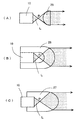
図3は、第1の実施の形態の発光ダイオード照明装置10を光源とする収束光形成の応用例を示す図であり、図3(A)は従来の光学レンズを用いた例、図3(B)はバルク型レンズを用いた例、図3(C)はレンズ状樹脂を用いた例を示す。
図3(A)において、発光ダイオード照明装置10に搭載した全ての発光ダイオードの発光Lが焦点Pに集光し、焦点Pを光源として、焦点距離だけ離して配設したレンズ25によって収束光線が形成される。
この構成によれば、発光ダイオード照明装置10に搭載した発光ダイオードの数に比例した強度の収束光が得られる。
図3(B)において、発光ダイオード照明装置10の焦点Pが、バルク型レンズ26の光源位置に一致するように配設されており、発光ダイオード照明装置10に搭載した全ての発光ダイオードの発光Lが、焦点Pに集光し、点Pを光源として、バルク型レンズ26により収束される。
【0016】
ここで、バルク型レンズについて説明する。バルク型レンズとは、発光体を内包するための空隙を有する例えば砲弾状のレンズで、空隙に内包したLED等の半導体発光素子の発光のほとんど全てを収束することができるもので、本出願人により開発されたものであり、その詳細については特願2001−20825号明細書が参照される。
図7は、バルク型レンズの構成を示す断面図である。
図において、バルク型レンズ70は、第1のレンズ面71と、第2のレンズ面72と、内側面73と、外側面74と、底面75の面から構成される、透明光学媒質76からなるバルク体である。第1のレンズ面71と第2のレンズ面72は、光のコリメート、収束又は発散と言った使用目的に応じたレンズ作用を有する曲面であり、図の例では、光学媒質76から見て、第1のレンズ面71は外に凸球面、第2のレンズ面72は凹球面である。内側面73と外側面74は、この例では、円筒面である。図は、LEDチップ77が支持台78上に支持されて、バルク型レンズ70に搭載されて発光し、その光束79が収束して出射している様子を示している。
【0017】
このバルク型レンズ70は、いわば、凸レンズ内に光源を内包している構造なので、光源に球面凸レンズを近づけて平行光線を形成する従来技術の場合に生ずる損失、すなわち、凸レンズの曲率半径と焦点距離の関係から定まる開口角以上の光束を収束することができないことによる損失が生じない。
また、光源に球面凸レンズを近づけて収束した場合には、レンズ面のフレネル反射光が空間に散逸してしまい、収束光として利用することができないが、バルク型レンズの場合には、バルク型レンズが凸レンズ内に光源を内包している構造であるので、第1のレンズ面71と第2のレンズ面72で生ずるフレネル反射光がバルク型レンズから散逸することが無く、その一部は、内側面73と外側面74及び底面75で反射して、再び第1のレンズ面71にもどって収束光となり、フレネル反射光の他の一部はLEDチップ77に戻り、LEDチップ77のpn接合で吸収されて再発光する。
従って、図3(B)の構成によれば、発光ダイオード照明装置10に搭載した発光ダイオードの発光をほとんど全て収束することができ、極めて効率良く高光強度の収束光が得られる。
【0018】
次に、図3(C)の構成を説明する。
図において、発光ダイオード照明装置10は、発光ダイオード照明装置10の発光面を覆ってレンズ状の透明又は半透明樹脂27が配設されている。
透明または半透明樹脂27は、透明または半透明プラスチック樹脂、透明性が高く適当な弾性を示すシリコーンポリマー、フッ素系ポリマー、熱可塑性エラストマー又は紫外線硬化性樹脂等である。
この構成によれば、発光ダイオード照明装置10に搭載した発光ダイオードの数に比例した高光強度の収束光が得られる。
【0019】
次に、本発明の発光ダイオード照明装置の第2の実施の形態を説明する。
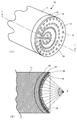
図4は本発明の発光ダイオード照明装置の第2の実施の形態を示す斜視図であり、図5は図4に示した発光ダイオード照明装置の断面図である。
図4において、発光ダイオード照明装置40は、第1の実施の形態における凹面状の基板13の代わりに、 環状の基板41を用い、環状の基板41の内面41a上にフェースボンディング型発光ダイオード16を環の円周方向に沿って配列したものであり、環央部には、環軸48を中心対称軸とした光の反射体43を備えている。また、環状の基板41は、図5に示したように放熱フィン41bを有していても良く、または図1で示したように、ペルチエー素子やヒートパイプ等の冷却手段を有していても良い。
【0020】
反射体43は、反射体43の環軸48を含む断面が環軸48に向かって凸状の2次曲線を有する回転曲面錐体であり、凸状の2次曲線はフェースボンディング型発光ダイオード16の取り付け位置を焦点とする放物線である。回転曲面錐体43は、光の出射方向、図においては右方向に頂点を有する。
反射体43は、筐体44の表面の一部を加工して形成し、環状の基板41は、基板41の環軸48を、反射体43の中心対称軸に一致させて筐体44にネジ止め固定されている例である。なお、反射体43を独立の部材として作製し、筐体44に取り付けてもよい。
【0021】
環状の基板41の内面41aは、絶縁体又は表面を絶縁体で覆った導体で構成されており、フェースボンディング型発光ダイオード16は、内面41a上に設けられた電源供給用の電極パターン42にボンディングして固定され、かつ電気的に接続されている。
電極パターン42は、リード線46に接続しており、取付固定部45の背面に設けた外部電源接続端子47に接続されている。
取付固定部45は、ネジ部45aを有し、ソケットにねじ込み固定できる。または、外部電源への接続は、ソケットに差し込んで固定する方式でも良い。
【0022】
これらの構成からなる第2の実施の形態の照明装置40によれば、図5に示すように、各発光ダイオード16から有限の発散角を有して発光した発光Lは、環軸48を含む面内の発散角に応じて反射体43の稜線43a上の異なった位置に入射する。稜線43aは、発光ダイオード16の取り付け位置を焦点とする放物線形状を有するから、稜線43aの異なった位置に入射した各発光は、各々、環軸48方向に反射され、高光強度の平行光線が得られる。
【0023】
次に、本発明の第2の実施の形態の他の例を説明する。
図6は、第2の実施の形態の他の例を示す斜視図である。
この例は、第2の実施の形態と比べ、反射体の形状が異なる。
図において、反射体53は、反射体53の環軸48を含む断面の稜線43aが環軸48に向かって凸状の2次曲線を有し、この2次曲線は発光ダイオード16の取り付け位置を焦点とする放物線形状を有しており、この2次曲線を2辺とする複数の曲平面53bからなる曲面角錐体である。
曲平面53bは、各々のフェースボンディング型発光ダイオード16の発光面と対向する位置に、フェースボンディング型発光ダイオード16の数だけ設けるのが好ましい。
【0024】
この構成からなる第2の実施の形態の照明装置50によれば、各々の発光ダイオード16から有限の発散角を有して発光した光は、環軸48を含む面内の発散角、及び環軸48に垂直な面内の発散角に応じて反射体53の各々の曲平面53b上の異なった位置に入射し、各々の曲平面53b上の異なった位置に入射した各々の発光は、曲平面53bが環軸48に向かって発光ダイオード16の取り付け位置を焦点とする放物線形状を有する2次曲線を2辺とする曲平面であるから、各々、環軸48方向に反射されて高光強度の平行光線が得られる。
【0025】
なお、上記第1及び第2の実施の形態において、発光波長の異なる発光ダイオードを複数取り混ぜて使用し、個々の発光ダイオードの発光を独立に制御すれば、所望の色相、色調の発光が得られることは明らかであり、また、反射体43,53の表面に微細な凹凸を設けることにより、所望の色相、色調の発光が得られることも明白である。
また、上記第1及び第2の実施の形態において、発光ダイオードとして、フェースボンディング型発光ダイオードを使用しているが、LEDチップの周囲を透明樹脂で凸レンズ形状にモールドした、いわゆるレンズ付発光ダイオードを用いて発光ダイオード照明装置を構成し、このようにして構成した照明装置をバルク型レンズに内包して搭載し得ることは明らかである。
本発明の照明装置は、光強度が高いので、遠方からも確認できることを必要とする信号機、あるいは表示装置などに使用すれば極めて有用である。
【0026】
【発明の効果】
上記説明から理解されるように、本発明の発光ダイオード照明装置によれば、高光強度の発光ダイオード照明装置が得られる。
特定の波長のLED光を大量に照射することが必要な、植物育成、生化学の分野、また、表示、装飾、舞台といった照明分野に使用すれば極めて有用である。
また、遠方からも確認できることが必要な信号機、あるいは表示装置に使用すれば極めて有用である。
【図面の簡単な説明】
【図1】本発明の発光ダイオード照明装置の第1の実施の形態を示すもので、(A)は外観斜視図、(B)は(A)のA−A断面模式図である。
【図2】本発明で用いるフェースボンディング型発光ダイオードの構成を示す断面図である。
【図3】第1の実施の形態の発光ダイオード照明装置を光源とする収束光形成の応用例を示し、(A)は従来の光学レンズを用いた例、(B)はバルク型レンズを用いた例、(C)はレンズ状樹脂を用いた例の概略図である。
【図4】本発明の発光ダイオード照明装置の第2の実施の形態を示す斜視図である。
【図5】図4に示した発光ダイオード照明装置の断面図である。
【図6】第2の実施の形態の他の例を示す斜視図である。
【図7】バルク型レンズの構成を示す断面図である。
【符号の説明】
10 第1の実施の形態による発光ダイオード照明装置
11 支持部
12 冷却部
13 基板
14 凹面
15 電極パターン
16 フェースボンディング型発光ダイオードチップ
17 透明基板
18 p又はn型半導体層
19 n又はp型半導体層
20 凹嵌部
21 発光ダイオードチップ電極
25 凸レンズ
26 バルク型レンズ
27 レンズ状透明樹脂
40 第2の実施の形態による発光ダイオード照明装置
41 環状の基板
41a 環状の基板の内面
41b 冷却フィン
42 電極パターン
43,53 反射体
43a 反射体の稜線
44 筐体
45 取付固定部
45a ネジ部
47 外部電源接続端子
48 環軸
50 第2の実施の形態による他の発光ダイオード照明装置
53b 曲平面
P 焦点
L 光束[0001]
BACKGROUND OF THE INVENTION
The present invention relates to a light-emitting diode illuminating device having a high light intensity, which is arranged so as to collect emitted light, such as a plurality of light-emitting diodes, for example, a face-bonding light-emitting diode or a light-emitting diode with lens.
[0002]
[Prior art]
Nowadays, LEDs (Light Emitting Diodes) having various emission wavelengths from infrared light to ultraviolet light are manufactured and widely used for optical communication, various displays, various illuminations, and the like.
As a feature of the LED, its emission spectrum has a narrower spectrum width than other conventional light sources, that is, high monochromaticity, and that a desired spectrum can be selected by combining LEDs having various emission wavelengths, and The light emitting efficiency is high and heat generation is small, and the demand for LED lighting devices that take advantage of these features is increasing.
For example, in plant cultivation, it is known that the growth rate of plants is significantly increased by irradiating a large amount of light having a specific wavelength, and plant cultivation farmers need a lighting device with high intensity at a specific wavelength. It is said.
Also, in the field of the biochemical industry, it is used for applications such as irradiating a large amount of light with specific wavelengths or different emission wavelengths at the same time to promote specific biochemical reactions and increase the production efficiency of chemicals, etc. There is a need for a lighting device that can be used.
Further, in the lighting field such as display, decoration, and stage, there is a need for a lighting device that can change color and tone arbitrarily, has high luminous efficiency, little heat generation, and high intensity that can be confirmed from a distance.
[0003]
Thus, LED lighting devices that can illuminate light of a specific wavelength with high intensity are required in various industrial fields.
However, the LED has a limitation due to the operation principle of passing a current through the semiconductor junction, and it is difficult to obtain an LED chip with sufficiently high light intensity that can be compared with a halogen lamp. A semiconductor light source with high light intensity includes LD (Laser Diode), but short wavelength LDs such as blue have disadvantages that it is difficult to produce an optical resonator and are difficult to obtain or are extremely expensive.
Thus, although the LED lighting apparatus with high light intensity is required, the LED lighting apparatus which has still sufficient light intensity is not implement | achieved.
[0004]
[Problems to be solved by the invention]
In view of the above problems, an object of the present invention is to provide a light-emitting diode illuminating device with high light intensity.
[0005]
[Means for Solving the Problems]
In order to achieve the above object, a light-emitting diode illuminating device of the present invention includes a bulk-type lens having a gap and a light source, and the bulk-type lens has a cylindrical outer surface and a first convex spherical surface. The lens surface has a cylindrical inner surface and a concave spherical second lens surface, and the cylindrical outer surface is configured to function as a reflecting surface, and the light source includes a plurality of light emitting diodes. Are arranged on the concave surface, and the light source is included in the gap of the bulk type lens.
According to this configuration, since the light emitting diodes densely arranged on the concave surface are included as the light source in the gap of the bulk type lens, an extremely efficient light emitting diode illuminating device can be realized.
[0007]
Further, in the present invention, it is preferable that a cooling means for promoting heat dissipation is provided on a fixing member of an electrode of a light emitting diode, particularly a face bonding type light emitting diode. This cooling means may be a Peltier element or a heat pipe.
Although the cooling means with these configurations does not have a high cooling capacity, it uses a face-bonding type light emitting diode that generates very little heat and dissipates heat. It does not require the bulky cooling device that is indispensable. Therefore, it is possible to realize a compact lighting device with extremely high light intensity.
[0009]
DETAILED DESCRIPTION OF THE INVENTION
Hereinafter, embodiments of the present invention will be described in detail with reference to the drawings. Note that substantially the same members will be described using the same reference numerals.
First, a first embodiment of the present invention will be described.
FIG. 1 is a diagram showing a first embodiment of a light-emitting diode illuminating device of the present invention, FIG. 1 (A) is an external perspective view, and FIG. 1 (B) is a cross-sectional view taken along line AA of FIG. . In FIG. 1A, the electrode pattern is not shown for easy viewing.
1A and 1B, a light-emitting diode
[0010]
Light emitting diodes inherently generate little heat, but if a large number of LEDs are densely arranged as in the present embodiment, countermeasures for heat generation must be taken, and therefore the
The
Further, the
[0011]
Here, the face bonding type light emitting diode will be described.
Light emitting diode chips include a wire bonding type and a face bonding type chip. The wire bonding type chip is one in which one or both of electrodes for applying a current to a pn junction and a power supply electrode of a substrate are connected by a bonding wire. For this reason, in the wire bonding type chip, there is a problem that the bonding wire blocks light emission and a uniform light intensity distribution cannot be obtained, and heat dissipation of the chip is performed through the bonding wire, so heat dissipation is poor. There is a problem that the chip temperature tends to rise.
[0012]
On the other hand, the face bonding type chip has both electrodes for applying a current to the pn junction on the chip back surface, and this electrode has a wide area that substantially occupies the entire chip back surface. Further, the face bonding type chip can be electrically connected and fixed simultaneously by thermocompression bonding the electrode on the back surface of the chip to the electrode pattern on the substrate. Therefore, if a face bonding type chip is used, the need for wire bonding is eliminated, the process is simplified, a uniform light intensity distribution is obtained because there is no bonding wire, and the contact area with the substrate is large. The heat dissipation is good and the chip temperature is hard to rise. The present invention can be applied to either the wire bonding type chip or the face bonding type chip described above, but the latter chip is more advantageous. Hereinafter, a face bonding type light emitting diode will be described as an example.
[0013]
FIG. 2 is a diagram showing a configuration of a face-bonding type light emitting diode used in the present embodiment.
In the figure, a face bonding type
In the face bonding type
Since the light emitting diode illuminating device according to the first embodiment of the present invention uses a face bonding type light emitting diode, the light intensity distribution is uniform and the temperature rise is small. Moreover, since the size is extremely small as compared with the LED with a lens using a bullet-type lens, it can be arranged with high density.
2 is not limited to the face bonding type
[0014]
According to the light-emitting
[0015]
Next, an application example of a face bonding type light emitting diode that obtains high intensity convergent light using the first embodiment will be described.
FIG. 3 is a diagram showing an application example of convergent light formation using the light-emitting
In FIG. 3A, the light emission L of all the light-emitting diodes mounted on the light-emitting
According to this configuration, convergent light having an intensity proportional to the number of light emitting diodes mounted on the light emitting
In FIG. 3B, the focal point P of the light-emitting
[0016]
Here, the bulk type lens will be described. A bulk lens is, for example, a bullet-shaped lens having a gap for containing a light emitter, and can converge almost all of the light emission of a semiconductor light emitting device such as an LED enclosed in the gap. The details of this have been developed by Japanese Patent Application No. 2001-20825.
FIG. 7 is a cross-sectional view showing the configuration of the bulk lens.
In the figure, the
[0017]
Since this
In addition, when a spherical convex lens is brought close to a light source and converged, Fresnel reflected light on the lens surface is scattered into space and cannot be used as convergent light. However, in the case of a bulk type lens, a bulk type lens is used. Since the light source is included in the convex lens, the Fresnel reflected light generated on the
Therefore, according to the configuration of FIG. 3B, almost all of the light emission of the light emitting diodes mounted on the light emitting
[0018]
Next, the configuration of FIG. 3C will be described.
In the figure, the light emitting
The transparent or
According to this configuration, convergent light with high light intensity proportional to the number of light emitting diodes mounted on the light emitting
[0019]
Next, a second embodiment of the light-emitting diode illuminating device of the present invention will be described.
FIG. 4 is a perspective view showing a second embodiment of the light-emitting diode illuminating device of the present invention, and FIG. 5 is a cross-sectional view of the light-emitting diode illuminating device shown in FIG.
In FIG. 4, the light-emitting
[0020]
The
The
[0021]
The inner surface 41a of the
The
The
[0022]
According to the
[0023]
Next, another example of the second embodiment of the present invention will be described.
FIG. 6 is a perspective view showing another example of the second embodiment.
In this example, the shape of the reflector is different from that of the second embodiment.
In the drawing, the
It is preferable to provide the
[0024]
According to the
[0025]
In the first and second embodiments, if a plurality of light emitting diodes having different light emission wavelengths are mixed and used, and light emission of each light emitting diode is controlled independently, light emission of a desired hue and color tone can be obtained. Obviously, it is also obvious that light emission having a desired hue and tone can be obtained by providing fine irregularities on the surfaces of the
In the first and second embodiments, a face bonding type light emitting diode is used as the light emitting diode. However, a so-called lens light emitting diode in which the periphery of the LED chip is molded into a convex lens shape with a transparent resin is used. It is obvious that a light-emitting diode illuminating device can be used, and the illuminating device thus configured can be included in a bulk type lens and mounted.
Since the illumination device of the present invention has a high light intensity, it is extremely useful when used for a traffic light or a display device that requires confirmation from a distance.
[0026]
【The invention's effect】
As understood from the above description, according to the light-emitting diode illuminating device of the present invention, a light-emitting diode illuminating device with high light intensity can be obtained.
It is extremely useful when used in the fields of plant growth and biochemistry, and in the lighting field such as display, decoration, and stage, where it is necessary to irradiate a large amount of LED light of a specific wavelength.
Further, it is extremely useful when used for a traffic light or display device that needs to be confirmed from a distance.
[Brief description of the drawings]
1A and 1B show a first embodiment of a light-emitting diode illuminating device of the present invention, in which FIG. 1A is an external perspective view, and FIG. 1B is a schematic cross-sectional view taken along line AA in FIG.
FIG. 2 is a cross-sectional view showing a configuration of a face-bonding type light emitting diode used in the present invention.
FIGS. 3A and 3B show an application example of convergent light formation using the light-emitting diode illuminating apparatus of the first embodiment as a light source, FIG. 3A shows an example using a conventional optical lens, and FIG. (C) is a schematic diagram of an example using a lenticular resin.
FIG. 4 is a perspective view showing a second embodiment of the light-emitting diode illuminating device of the present invention.
5 is a cross-sectional view of the light-emitting diode illuminating device shown in FIG.
FIG. 6 is a perspective view showing another example of the second embodiment.
FIG. 7 is a cross-sectional view showing a configuration of a bulk type lens.
[Explanation of symbols]
DESCRIPTION OF
Claims (3)
上記バルク型レンズは、円筒状の外側面と外に凸球面状の第一のレンズ面、及び、円筒状の内側面と凹球面状の第二のレンズ面を有していて、上記円筒状の外側面は反射面として機能するよう構成されて成り、 The bulk type lens has a cylindrical outer surface, a first convex spherical lens surface, and a cylindrical inner surface and a concave second lens surface. The outer surface of is configured to function as a reflective surface,
上記光源は、複数の発光ダイオードが凹面上に配列されて成り、 The light source comprises a plurality of light emitting diodes arranged on a concave surface,
上記光源が、上記バルク型レンズの上記空隙に内包されていること特徴とする、発光ダイオード照明装置。 The light-emitting diode illuminating device, wherein the light source is included in the gap of the bulk lens.
Priority Applications (1)
| Application Number | Priority Date | Filing Date | Title |
|---|---|---|---|
| JP2001218049A JP4129570B2 (en) | 2001-07-18 | 2001-07-18 | Light emitting diode lighting device |
Applications Claiming Priority (1)
| Application Number | Priority Date | Filing Date | Title |
|---|---|---|---|
| JP2001218049A JP4129570B2 (en) | 2001-07-18 | 2001-07-18 | Light emitting diode lighting device |
Publications (2)
| Publication Number | Publication Date |
|---|---|
| JP2003031005A JP2003031005A (en) | 2003-01-31 |
| JP4129570B2 true JP4129570B2 (en) | 2008-08-06 |
Family
ID=19052285
Family Applications (1)
| Application Number | Title | Priority Date | Filing Date |
|---|---|---|---|
| JP2001218049A Expired - Fee Related JP4129570B2 (en) | 2001-07-18 | 2001-07-18 | Light emitting diode lighting device |
Country Status (1)
| Country | Link |
|---|---|
| JP (1) | JP4129570B2 (en) |
Cited By (1)
| Publication number | Priority date | Publication date | Assignee | Title |
|---|---|---|---|---|
| US9713476B2 (en) | 2007-09-25 | 2017-07-25 | Polyzen Inc. | Multi-layer film welded articulated balloon |
Families Citing this family (33)
| Publication number | Priority date | Publication date | Assignee | Title |
|---|---|---|---|---|
| US7320632B2 (en) | 2000-06-15 | 2008-01-22 | Lednium Pty Limited | Method of producing a lamp |
| AUPQ818100A0 (en) | 2000-06-15 | 2000-07-06 | Arlec Australia Limited | Led lamp |
| CA2488904A1 (en) * | 2002-06-14 | 2003-12-24 | Lednium Pty Ltd | A lamp and method of producing a lamp |
| TW200510772A (en) * | 2003-09-02 | 2005-03-16 | Delta Electronics Inc | Polarized light source |
| DE10344547A1 (en) * | 2003-09-24 | 2005-08-11 | Warnking Elektrotechnik Gmbh | Room lighting source, is arranged with circuit board crossing long axis of light source |
| JP4804429B2 (en) * | 2003-12-05 | 2011-11-02 | 三菱電機株式会社 | Light emitting device and lighting apparatus using the same |
| KR100731454B1 (en) * | 2003-12-05 | 2007-06-21 | 미츠비시덴키 가부시키가이샤 | Light emitting device and illumination instrument using the same |
| CA2591569A1 (en) * | 2003-12-16 | 2005-06-30 | 1662801 Ontario Inc. | Lighting assembly, heat sink and heat recovery system therefor |
| US7040782B2 (en) * | 2004-02-19 | 2006-05-09 | Gelcore, Llc | Off-axis parabolic reflector |
| US7237927B2 (en) * | 2004-06-17 | 2007-07-03 | Osram Sylvania Inc. | Light emitting diode lamp with conically focused light guides |
| JP4693152B2 (en) * | 2005-04-27 | 2011-06-01 | シチズン電子株式会社 | Light emitting diode |
| JP4607811B2 (en) * | 2006-04-18 | 2011-01-05 | 株式会社小糸製作所 | Lighting fixtures for vehicles |
| EP2031295A1 (en) * | 2007-08-29 | 2009-03-04 | Asetronics AG | Medical, in particular dental treatment lamp |
| DE102007053790B3 (en) * | 2007-11-12 | 2009-05-07 | Siteco Beleuchtungstechnik Gmbh | LED luminaire for the design of the light distribution |
| JPWO2009125618A1 (en) * | 2008-04-11 | 2011-08-04 | ハリソン東芝ライティング株式会社 | Light emitting device |
| JP2009266863A (en) * | 2008-04-22 | 2009-11-12 | Minami Kk | Led light-emitting object |
| US8013501B2 (en) | 2008-06-04 | 2011-09-06 | Forever Bulb, Llc | LED-based light bulb device |
| US8186852B2 (en) | 2009-06-24 | 2012-05-29 | Elumigen Llc | Opto-thermal solution for multi-utility solid state lighting device using conic section geometries |
| EP2339224B1 (en) * | 2009-12-22 | 2016-10-26 | Zumtobel Lighting GmbH | Assembly for emitting light |
| JP2011222942A (en) * | 2010-04-12 | 2011-11-04 | Tyntek Corp | Reflective light-emitting diode lamp |
| JP2012022802A (en) * | 2010-07-12 | 2012-02-02 | Harison Toshiba Lighting Corp | Light source device |
| EP2450612B1 (en) * | 2010-11-08 | 2014-04-30 | LG Innotek Co., Ltd. | Lighting apparatus |
| WO2012092140A2 (en) | 2010-12-30 | 2012-07-05 | Elumigen Llc | Light assembly having light sources and adjacent light tubes |
| JP5640751B2 (en) * | 2011-01-11 | 2014-12-17 | 東芝ライテック株式会社 | lighting equipment |
| JP2012226943A (en) * | 2011-04-19 | 2012-11-15 | Panasonic Corp | Lighting fixture |
| CN102767704A (en) * | 2011-05-04 | 2012-11-07 | 鼎元光电科技股份有限公司 | Reverse type lamp |
| DK2718616T3 (en) | 2011-06-09 | 2016-01-25 | Elumigen Llc | The semiconductor lighting device, which uses hot channels in a housing |
| DE102012109146A1 (en) * | 2012-09-27 | 2014-03-27 | Osram Opto Semiconductors Gmbh | Ring light module and method for producing a ring light module |
| DE102012109149A1 (en) * | 2012-09-27 | 2014-03-27 | Osram Opto Semiconductors Gmbh | Ring light module and method for producing a ring light module |
| US9651219B2 (en) | 2014-08-20 | 2017-05-16 | Elumigen Llc | Light bulb assembly having internal redirection element for improved directional light distribution |
| CN108807359A (en) * | 2018-07-26 | 2018-11-13 | 中山市光圣半导体科技有限责任公司 | A kind of LED component and manufacturing method |
| DE102019135527A1 (en) * | 2019-12-20 | 2021-06-24 | BILTON International GmbH | Lighting device |
| WO2023021749A1 (en) * | 2021-08-17 | 2023-02-23 | 株式会社 レイマック | Lighting device for inspection |
-
2001
- 2001-07-18 JP JP2001218049A patent/JP4129570B2/en not_active Expired - Fee Related
Cited By (1)
| Publication number | Priority date | Publication date | Assignee | Title |
|---|---|---|---|---|
| US9713476B2 (en) | 2007-09-25 | 2017-07-25 | Polyzen Inc. | Multi-layer film welded articulated balloon |
Also Published As
| Publication number | Publication date |
|---|---|
| JP2003031005A (en) | 2003-01-31 |
Similar Documents
| Publication | Publication Date | Title |
|---|---|---|
| JP4129570B2 (en) | Light emitting diode lighting device | |
| US7275841B2 (en) | Utility lamp | |
| US8330342B2 (en) | Spherical light output LED lens and heat sink stem system | |
| JP4376289B2 (en) | Light irradiation device | |
| US9091420B2 (en) | Illumination apparatus | |
| US6527419B1 (en) | LED spotlight illumination system | |
| US6974234B2 (en) | LED lighting assembly | |
| US7766505B2 (en) | Light source assembly | |
| KR101377965B1 (en) | Lighting apparatus | |
| TW568989B (en) | Linear illuminating device | |
| JP3686660B2 (en) | Light irradiation device and optical unit | |
| US20060044806A1 (en) | Light emitting diode system packages | |
| US20050201100A1 (en) | Led lighting assembly | |
| US20100165635A1 (en) | Led unit | |
| JP5097916B2 (en) | Lighting device | |
| JP2008004415A (en) | Three dimensional light source body | |
| JP2009135080A (en) | Light source device | |
| JP4905751B2 (en) | Dental light irradiator | |
| US20040190290A1 (en) | Optical assembly for light emitting diode package | |
| JP2015111523A (en) | Lighting device and optical lens | |
| JP7088964B2 (en) | High irradiance lighting assembly | |
| JP2001007406A (en) | Light emitting diode array | |
| IE84147B1 (en) | A utility lamp | |
| IES84104Y1 (en) | A utility lamp | |
| CN111355119A (en) | Convergence integrated laser device |
Legal Events
| Date | Code | Title | Description |
|---|---|---|---|
| A621 | Written request for application examination |
Free format text: JAPANESE INTERMEDIATE CODE: A621 Effective date: 20040902 |
|
| A977 | Report on retrieval |
Free format text: JAPANESE INTERMEDIATE CODE: A971007 Effective date: 20070823 |
|
| A131 | Notification of reasons for refusal |
Free format text: JAPANESE INTERMEDIATE CODE: A131 Effective date: 20070904 |
|
| A521 | Request for written amendment filed |
Free format text: JAPANESE INTERMEDIATE CODE: A523 Effective date: 20071105 |
|
| TRDD | Decision of grant or rejection written | ||
| A01 | Written decision to grant a patent or to grant a registration (utility model) |
Free format text: JAPANESE INTERMEDIATE CODE: A01 Effective date: 20080415 |
|
| A01 | Written decision to grant a patent or to grant a registration (utility model) |
Free format text: JAPANESE INTERMEDIATE CODE: A01 |
|
| A61 | First payment of annual fees (during grant procedure) |
Free format text: JAPANESE INTERMEDIATE CODE: A61 Effective date: 20080502 |
|
| R150 | Certificate of patent or registration of utility model |
Free format text: JAPANESE INTERMEDIATE CODE: R150 |
|
| FPAY | Renewal fee payment (event date is renewal date of database) |
Free format text: PAYMENT UNTIL: 20110530 Year of fee payment: 3 |
|
| S202 | Request for registration of non-exclusive licence |
Free format text: JAPANESE INTERMEDIATE CODE: R315201 |
|
| FPAY | Renewal fee payment (event date is renewal date of database) |
Free format text: PAYMENT UNTIL: 20110530 Year of fee payment: 3 |
|
| R350 | Written notification of registration of transfer |
Free format text: JAPANESE INTERMEDIATE CODE: R350 |
|
| FPAY | Renewal fee payment (event date is renewal date of database) |
Free format text: PAYMENT UNTIL: 20110530 Year of fee payment: 3 |
|
| FPAY | Renewal fee payment (event date is renewal date of database) |
Free format text: PAYMENT UNTIL: 20110530 Year of fee payment: 3 |
|
| FPAY | Renewal fee payment (event date is renewal date of database) |
Free format text: PAYMENT UNTIL: 20120530 Year of fee payment: 4 |
|
| FPAY | Renewal fee payment (event date is renewal date of database) |
Free format text: PAYMENT UNTIL: 20120530 Year of fee payment: 4 |
|
| FPAY | Renewal fee payment (event date is renewal date of database) |
Free format text: PAYMENT UNTIL: 20120530 Year of fee payment: 4 |
|
| FPAY | Renewal fee payment (event date is renewal date of database) |
Free format text: PAYMENT UNTIL: 20120530 Year of fee payment: 4 |
|
| FPAY | Renewal fee payment (event date is renewal date of database) |
Free format text: PAYMENT UNTIL: 20130530 Year of fee payment: 5 |
|
| FPAY | Renewal fee payment (event date is renewal date of database) |
Free format text: PAYMENT UNTIL: 20130530 Year of fee payment: 5 |
|
| LAPS | Cancellation because of no payment of annual fees |