JP4127232B2 - Level shifter, level shift circuit, electro-optical device, and electronic apparatus - Google Patents
Level shifter, level shift circuit, electro-optical device, and electronic apparatus Download PDFInfo
- Publication number
- JP4127232B2 JP4127232B2 JP2004109223A JP2004109223A JP4127232B2 JP 4127232 B2 JP4127232 B2 JP 4127232B2 JP 2004109223 A JP2004109223 A JP 2004109223A JP 2004109223 A JP2004109223 A JP 2004109223A JP 4127232 B2 JP4127232 B2 JP 4127232B2
- Authority
- JP
- Japan
- Prior art keywords
- signal
- selection signal
- level
- becomes active
- sel
- Prior art date
- Legal status (The legal status is an assumption and is not a legal conclusion. Google has not performed a legal analysis and makes no representation as to the accuracy of the status listed.)
- Expired - Lifetime
Links
- 230000015654 memory Effects 0.000 claims description 69
- 239000003990 capacitor Substances 0.000 claims description 12
- 230000005764 inhibitory process Effects 0.000 claims description 3
- 238000010586 diagram Methods 0.000 description 16
- 239000004973 liquid crystal related substance Substances 0.000 description 14
- 238000006243 chemical reaction Methods 0.000 description 7
- 230000006870 function Effects 0.000 description 6
- 102100022375 Dentin matrix acidic phosphoprotein 1 Human genes 0.000 description 4
- 101000804518 Homo sapiens Cyclin-D-binding Myb-like transcription factor 1 Proteins 0.000 description 4
- 101000901629 Homo sapiens Dentin matrix acidic phosphoprotein 1 Proteins 0.000 description 4
- 239000011159 matrix material Substances 0.000 description 4
- 239000000758 substrate Substances 0.000 description 4
- 230000007257 malfunction Effects 0.000 description 3
- 239000010409 thin film Substances 0.000 description 3
- 230000008859 change Effects 0.000 description 2
- 230000000694 effects Effects 0.000 description 2
- 239000000463 material Substances 0.000 description 2
- 230000007704 transition Effects 0.000 description 2
- 230000009471 action Effects 0.000 description 1
- 230000005540 biological transmission Effects 0.000 description 1
- 230000015572 biosynthetic process Effects 0.000 description 1
- 230000001413 cellular effect Effects 0.000 description 1
- 239000003086 colorant Substances 0.000 description 1
- 230000008878 coupling Effects 0.000 description 1
- 238000010168 coupling process Methods 0.000 description 1
- 238000005859 coupling reaction Methods 0.000 description 1
- 239000000382 optic material Substances 0.000 description 1
- 230000009467 reduction Effects 0.000 description 1
Images


Classifications
-
- G—PHYSICS
- G09—EDUCATION; CRYPTOGRAPHY; DISPLAY; ADVERTISING; SEALS
- G09G—ARRANGEMENTS OR CIRCUITS FOR CONTROL OF INDICATING DEVICES USING STATIC MEANS TO PRESENT VARIABLE INFORMATION
- G09G3/00—Control arrangements or circuits, of interest only in connection with visual indicators other than cathode-ray tubes
- G09G3/20—Control arrangements or circuits, of interest only in connection with visual indicators other than cathode-ray tubes for presentation of an assembly of a number of characters, e.g. a page, by composing the assembly by combination of individual elements arranged in a matrix no fixed position being assigned to or needed to be assigned to the individual characters or partial characters
- G09G3/34—Control arrangements or circuits, of interest only in connection with visual indicators other than cathode-ray tubes for presentation of an assembly of a number of characters, e.g. a page, by composing the assembly by combination of individual elements arranged in a matrix no fixed position being assigned to or needed to be assigned to the individual characters or partial characters by control of light from an independent source
- G09G3/36—Control arrangements or circuits, of interest only in connection with visual indicators other than cathode-ray tubes for presentation of an assembly of a number of characters, e.g. a page, by composing the assembly by combination of individual elements arranged in a matrix no fixed position being assigned to or needed to be assigned to the individual characters or partial characters by control of light from an independent source using liquid crystals
- G09G3/3611—Control of matrices with row and column drivers
- G09G3/3685—Details of drivers for data electrodes
- G09G3/3688—Details of drivers for data electrodes suitable for active matrices only
-
- F—MECHANICAL ENGINEERING; LIGHTING; HEATING; WEAPONS; BLASTING
- F16—ENGINEERING ELEMENTS AND UNITS; GENERAL MEASURES FOR PRODUCING AND MAINTAINING EFFECTIVE FUNCTIONING OF MACHINES OR INSTALLATIONS; THERMAL INSULATION IN GENERAL
- F16C—SHAFTS; FLEXIBLE SHAFTS; ELEMENTS OR CRANKSHAFT MECHANISMS; ROTARY BODIES OTHER THAN GEARING ELEMENTS; BEARINGS
- F16C19/00—Bearings with rolling contact, for exclusively rotary movement
- F16C19/02—Bearings with rolling contact, for exclusively rotary movement with bearing balls essentially of the same size in one or more circular rows
- F16C19/14—Bearings with rolling contact, for exclusively rotary movement with bearing balls essentially of the same size in one or more circular rows for both radial and axial load
- F16C19/16—Bearings with rolling contact, for exclusively rotary movement with bearing balls essentially of the same size in one or more circular rows for both radial and axial load with a single row of balls
-
- F—MECHANICAL ENGINEERING; LIGHTING; HEATING; WEAPONS; BLASTING
- F16—ENGINEERING ELEMENTS AND UNITS; GENERAL MEASURES FOR PRODUCING AND MAINTAINING EFFECTIVE FUNCTIONING OF MACHINES OR INSTALLATIONS; THERMAL INSULATION IN GENERAL
- F16C—SHAFTS; FLEXIBLE SHAFTS; ELEMENTS OR CRANKSHAFT MECHANISMS; ROTARY BODIES OTHER THAN GEARING ELEMENTS; BEARINGS
- F16C33/00—Parts of bearings; Special methods for making bearings or parts thereof
- F16C33/30—Parts of ball or roller bearings
- F16C33/58—Raceways; Race rings
- F16C33/60—Raceways; Race rings divided or split, e.g. comprising two juxtaposed rings
-
- G—PHYSICS
- G09—EDUCATION; CRYPTOGRAPHY; DISPLAY; ADVERTISING; SEALS
- G09G—ARRANGEMENTS OR CIRCUITS FOR CONTROL OF INDICATING DEVICES USING STATIC MEANS TO PRESENT VARIABLE INFORMATION
- G09G2310/00—Command of the display device
- G09G2310/02—Addressing, scanning or driving the display screen or processing steps related thereto
- G09G2310/0264—Details of driving circuits
- G09G2310/0289—Details of voltage level shifters arranged for use in a driving circuit
-
- G—PHYSICS
- G09—EDUCATION; CRYPTOGRAPHY; DISPLAY; ADVERTISING; SEALS
- G09G—ARRANGEMENTS OR CIRCUITS FOR CONTROL OF INDICATING DEVICES USING STATIC MEANS TO PRESENT VARIABLE INFORMATION
- G09G2310/00—Command of the display device
- G09G2310/02—Addressing, scanning or driving the display screen or processing steps related thereto
- G09G2310/0264—Details of driving circuits
- G09G2310/0297—Special arrangements with multiplexing or demultiplexing of display data in the drivers for data electrodes, in a pre-processing circuitry delivering display data to said drivers or in the matrix panel, e.g. multiplexing plural data signals to one D/A converter or demultiplexing the D/A converter output to multiple columns
Description
本発明は、消費電力を低減することが可能なレベルシフタ、レベルシフト回路、電気光
学装置、及び電子機器に関する。
The present invention relates to a level shifter, a level shift circuit, an electro-optical device, and an electronic apparatus that can reduce power consumption.
近年、ブラウン管を備えた表示装置の代わりに、液晶や有機発光ダイオード等の電気光
学素子を備えた電気光学装置が普及しつつある。電気光学装置はパッシブマトリクス型と
アクティブマトリクス型に大別される。アクティブマトリクス型の電気光学装置は、行方
向に延在する走査線と、列方向に延在するデータ線との交差に対応して画素電極が形成さ
れる。更に、当該交差部分にあって画素電極とデータ線との間に、走査線に供給される走
査信号にしたがってオンオフする薄膜トランジスタが設けられる。加えて、画素電極に対
応する対向電極が設けられており、画素電極と対向電極との間には電気光学物質が介挿さ
れている。
In recent years, instead of a display device including a cathode ray tube, an electro-optical device including an electro-optical element such as a liquid crystal or an organic light emitting diode is becoming widespread. Electro-optical devices are roughly classified into a passive matrix type and an active matrix type. In the active matrix electro-optical device, pixel electrodes are formed corresponding to intersections between scanning lines extending in the row direction and data lines extending in the column direction. Further, a thin film transistor that is turned on and off in accordance with a scanning signal supplied to the scanning line is provided between the pixel electrode and the data line at the intersection. In addition, a counter electrode corresponding to the pixel electrode is provided, and an electro-optical material is interposed between the pixel electrode and the counter electrode.
電気光学物質や薄膜トランジスタを駆動するためには、比較的高い電圧が要求される。
一方、電気光学装置に、駆動の基準となるクロック信号や制御信号などを供給する外部制
御回路は、通常、CMOS回路で構成されるため、その論理信号の振幅は3〜5V程度で
ある。したがって、電気光学装置は、振幅変換回路(以下、単に「レベルシフタ」という
)を用いて、低振幅の論理信号を高振幅の論理信号に変換するのが一般的である。
In order to drive the electro-optic material and the thin film transistor, a relatively high voltage is required.
On the other hand, an external control circuit that supplies a clock signal, a control signal, or the like that serves as a driving reference to the electro-optical device is usually composed of a CMOS circuit, and the amplitude of the logic signal is about 3 to 5V. Therefore, an electro-optical device generally converts a low-amplitude logic signal into a high-amplitude logic signal using an amplitude conversion circuit (hereinafter simply referred to as “level shifter”).
このようなレベルシフタとしては、入力信号を交流結合により取り込むタイプのものが
知られている(例えば、特許文献1)。
ところで、レベルシフタは信号レベルを変換するものであるが、変換の対象となる信号
の作用によっては、常に動作する必要がないことがある。例えば、カラー表示の電気光学
装置においてはデータ線駆動回路からR,G,Bの各色に対応するデータ線信号を多重し
て1個の出力端子から出力し、多重されたデータ線信号をRGB用のデータ線に各々分配
するためにデマルチプレクサを用いることがある。デマルチプレクサは、排他的にアクテ
ィブとなるRGB用の色選択信号に従ってデータ線信号を各色のデータ線に出力する。こ
の場合、レベルシフタを用いて色選択信号の信号レベルを変換するのが一般的である。こ
のような場合、レベルシフタは、常に動作している必要はなく、入力される色選択信号が
アクティブとなる期間だけ動作していればよい。
By the way, the level shifter converts the signal level, but it may not always need to operate depending on the action of the signal to be converted. For example, in a color display electro-optical device, a data line signal corresponding to each color of R, G, B is multiplexed from a data line driving circuit and output from one output terminal, and the multiplexed data line signal is used for RGB. In some cases, a demultiplexer is used to distribute the data lines. The demultiplexer outputs data line signals to the data lines of the respective colors in accordance with RGB color selection signals that are exclusively active. In this case, the signal level of the color selection signal is generally converted using a level shifter. In such a case, the level shifter does not need to be always operated, and only needs to be operated during a period in which the input color selection signal is active.
一方、従来のレベルシフタは、電源が投入されると、一部のトランジスタが完全にオフ
していなので、ソース・ドレイン間に微小な電流が流れていた。このため、本来であれば
動作する必要がない期間に電力が消費されるという問題があった。
On the other hand, in the conventional level shifter, when the power is turned on, a part of the transistors are completely turned off, so that a minute current flows between the source and the drain. For this reason, there is a problem that power is consumed during a period when it is not necessary to operate.
本発明は上述した問題に鑑みてなされたものであり、消費電力の少ないレベルシフタ、
レベルシフト回路、電気光学装置、及び電子機器を提供することを解決課題とする。
The present invention has been made in view of the above-described problems, and is a level shifter with low power consumption.
It is an object to provide a level shift circuit, an electro-optical device, and an electronic apparatus.
本発明に係るレベルシフト回路は、時間軸に沿って順次、排他的にアクティブとなる複
数の選択信号SEL(1),SEL(2),…,SEL(N)(ただし、Nは正の整数)
が各々供給され、前記選択信号の信号レベルを変換して各々出力する複数のレベルシフタ
と、前記複数のレベルシフタの各々へ動作状態を制御する制御信号を供給する複数の制御
回路と、を備え、前記複数の選択信号SEL(1),SEL(2),…,SEL(N)は
、そのうちの選択信号SEL(N)がアクティブとなった後には選択信号SEL(1)が
アクティブとなるというが如く、その番号1,2,…,Nについて円環的にアクティブと
なり、前記複数の制御回路の各々は、
対応するレベルシフタに供給される選択信号SEL(t)(ただし、tは、1,2,…
,Nのいずれか)がアクティブとなる前にアクティブとなる先行選択信号SEL(t−1
)(ただし、t=1のときは、この(t−1)はNとする。)を用いて動作許可状態を指
示する前記制御信号を生成し、前記選択信号SEL(t)がアクティブとなった後にアク
ティブとなる後行選択信号SEL(t+1)(ただし、t=Nのときは、この(t+1)
は1とする。)を用いて対応する動作禁止状態を指示する前記制御信号を生成して、当該
制御信号を、対応するレベルシフタに供給することにより、当該レベルシフタの動作許可
及び動作禁止を、前記選択信号SEL(1),SEL(2),…,SEL(N)のみを用
いて行う、ことを特徴とする。
Level shift circuit according to the present invention, sequentially along the time axis, a plurality of the exclusive active selection signal SEL (1), SEL (2 ), ..., SEL (N) ( however, N is the positive integer)
There are respectively supplied, said comprising a plurality of level shifters for each converts the signal level of the selection signals, and a plurality of control circuits for supplying control signals for controlling the operating state to each of the plurality of level shifters, the The plurality of selection signals SEL (1), SEL (2),.
After the selection signal SEL (N) becomes active, the selection signal SEL (1)
As if it were active, the
Becomes, each of the plurality of control circuits,
Selection signal SEL (t) supplied to the corresponding level shifter (where t is 1, 2,...
, N) becomes a pre-selection signal SEL (t−1 ) that becomes active before it becomes active.
) (However, when t = 1, this (t−1) is N) , the control signal for instructing the operation permission state is generated, and the selection signal SEL (t) becomes active. The succeeding row selection signal SEL (t + 1) that becomes active after (when t = N, this (t + 1)
Is 1. ) And generates said control signal instructing the corresponding operation inhibition state by using, the
Permits operation of a level shifter by supplying a control signal to the corresponding level shifter
In addition, only the selection signals SEL (1), SEL (2),..., SEL (N) are used to prohibit operation.
It has carried out, characterized in that.
複数の選択信号は順次アクティブとなるので、レベルシフタは常に動作する必要はなく
、入力される選択信号がアクティブになる期間だけ動作すればよい。この発明によれば、
制御回路は、ある選択信号を基準としたとき、これに先行する先行選択信号を用いてレベ
ルシフタの動作を許可する一方、これに後行する後行選択信号を用いてレベルシフタの動
作を禁止する。従って、レベルシフタは必要な期間に動作し、不要な期間は動作を停止す
る。これにより、レベルシフタを常時動作させる場合と比較して消費電力を削減すること
ができる。
Since the plurality of selection signals are sequentially activated, the level shifter does not always have to operate, and only needs to operate during a period in which the input selection signal is active. According to this invention,
When a certain selection signal is used as a reference, the control circuit permits the operation of the level shifter using the preceding selection signal that precedes the selection signal, while prohibiting the operation of the level shifter using the subsequent selection signal that follows this. Therefore, the level shifter operates during a necessary period and stops operating during an unnecessary period. Thereby, power consumption can be reduced compared with the case where a level shifter is always operated.
ここで、前記先行選択信号は、対応するレベルシフタに供給される選択信号がアクティ
ブとなる直前にアクティブとなり、前記後行選択信号は、対応するレベルシフタに供給さ
れる選択信号がアクティブとなる直後にアクティブとなることが好ましい。この場合には
、
消費電力を最も効率良く削減することが可能となる。
Here, the preceding selection signal becomes active immediately before the selection signal supplied to the corresponding level shifter becomes active, and the subsequent selection signal becomes active immediately after the selection signal supplied to the corresponding level shifter becomes active. It is preferable that In this case,
The power consumption can be reduced most efficiently.
また、前記制御回路は、前記レベルシフタに供給される選択信号を用いて前記制御信号
を生成してもよいし、或いは、前記レベルシフタから出力される選択信号を用いて前記制
御信号を生成してもよい。制御回路は、対応するレベルシフタが動作する期間を特定でき
ればよいので、タイミングを特定する選択信号はレベル変換の前であっても後であっても
よい。
The control circuit may generate the control signal using a selection signal supplied to the level shifter, or may generate the control signal using a selection signal output from the level shifter. Good. Since the control circuit only needs to be able to specify the period during which the corresponding level shifter operates, the selection signal for specifying the timing may be before or after the level conversion.
また、上述したレベルシフト回路において、前記制御回路は動作状態を記憶するメモリ
回路を備え、前記メモリ回路は、前記先行選択信号がアクティブなると動作許可状態を記
憶し、前記後行選択信号がアクティブになると動作禁止状態を記憶し、記憶内容に応じた
信号を前記制御信号として出力することが好ましい。この場合は、メモリにレベルシフタ
の動作状態を記憶して、これに従ってレベルシフタを制御することができる。
In the above-described level shift circuit, the control circuit includes a memory circuit that stores an operation state. The memory circuit stores an operation permission state when the preceding selection signal becomes active, and the subsequent selection signal becomes active. In this case, it is preferable to store the operation prohibited state and output a signal corresponding to the stored content as the control signal. In this case, the operation state of the level shifter can be stored in the memory, and the level shifter can be controlled accordingly.
ここで、複数のメモリ回路のうち、所定のメモリ回路の記憶内容を動作許可状態にセッ
トし、他のメモリ回路の記憶内容を動作禁止状態にリセットする初期化動作を実行する初
期化手段を備えることが好ましい。レベルシフト回路に電源が投入された直後において、
メモリ回路の記憶内容は、一意に定めることができないため、全てのメモリ回路の記憶内
容が動作禁止状態を指示することもあり得る。この場合、全てのレベルシフタの動作は禁
止されるので、選択信号がアクティブになってもレベル変換が実行されない。この発明に
よれば、初期化手段を備えるので、そのような不都合を解消することができる。しかも、
初期化手段は、所定のメモリ回路の記憶内容のみを動作許可状態にセットするから、所定
のメモリ回路に対応するレベルシフタのみを動作させ、他のレベルシフタの動作を停止さ
せる。選択信号は順次アクティブとなるから、電源投入後に最初にアクティブとなる選択
信号が供給されるレベルシフタを動作させるように所定のメモリ回路を設定すればよい。
これによって、消費電力を削減しつつ、電源投入時の誤動作を防止することができる。
Here, an initialization unit is provided that performs an initialization operation of setting a memory content of a predetermined memory circuit to an operation-permitted state among a plurality of memory circuits and resetting a memory content of another memory circuit to an operation-inhibited state. It is preferable. Immediately after the power is turned on to the level shift circuit,
Since the memory contents of the memory circuit cannot be uniquely determined, the memory contents of all the memory circuits may indicate an operation prohibited state. In this case, since the operation of all level shifters is prohibited, the level conversion is not executed even if the selection signal becomes active. According to the present invention, since the initialization means is provided, such inconvenience can be solved. Moreover,
Since the initialization means sets only the stored contents of the predetermined memory circuit to the operation-permitted state, only the level shifter corresponding to the predetermined memory circuit is operated and the operations of the other level shifters are stopped. Since the selection signals are sequentially activated, a predetermined memory circuit may be set to operate the level shifter to which the selection signal that is activated first after power-on is supplied.
As a result, it is possible to prevent malfunction at power-on while reducing power consumption.
次に、本発明に係わるレベルシフタは、入力信号の信号レベルを変換して出力信号を出
力するレベルシフタであって、前記入力信号が一端に供給される第1容量素子と、一端が
前記第1容量素子の一端と接続される第2容量素子と、ゲートが前記第1容量素子の他端
と接続され、ソースが高電位供給線と接続される第1トランジスタと、ゲートが前記第2
容量素子の他端と接続され、ソースが低電位供給線と接続され、前記ドレインが第1トラ
ンジスタのドレインと接続される第2トランジスタと、前記高電位供給線と前記低電位供
給線から電源が供給され、制御信号に基づいて前記電源の供給を受けるか否かが制御され
、入力端と出力端とが前記第1トランジスタのゲートと接続される第1クロックドインバ
ータと、前記高電位供給線と前記低電位供給線から電源が供給され、制御信号に基づいて
前記電源の供給を受けるか否かが制御され、入力端と出力端が前記第2トランジスタのゲ
ートと接続される第2クロックドインバータと、前記第1トランジスタ及び前記第2トラ
ンジスタのドレインと入力端が接続され、出力端から前記出力信号を出力するインバータ
とを、備えることを特徴とする。
Next, a level shifter according to the present invention is a level shifter that converts the signal level of an input signal and outputs an output signal, the first capacitive element to which the input signal is supplied at one end, and the first capacitor at one end. A second capacitor connected to one end of the device; a gate connected to the other end of the first capacitor; a source connected to a high potential supply line; and a gate connected to the second capacitor.
A power source is connected to the other end of the capacitive element, a source is connected to the low potential supply line, the drain is connected to the drain of the first transistor, and the high potential supply line and the low potential supply line A first clocked inverter having an input terminal and an output terminal connected to a gate of the first transistor, and a high-potential supply line. Power is supplied from the low-potential supply line, and whether or not to receive the power supply is controlled based on a control signal, and a second clocked signal whose input terminal and output terminal are connected to the gate of the second transistor is controlled. An inverter; and an inverter connected to a drain and an input terminal of the first transistor and the second transistor and outputting the output signal from an output terminal. .
このレベルシフタによれば、第1クロックドインバータは第1トランジスタのゲートに
対してオフセット電圧(バイアス電圧)を付与する手段として機能し、第2クロックドイ
ンバータは第2トランジスタのゲートに対してオフセット電圧(バイアス電圧)を付与す
る手段として機能する。そして、第1及び第2クロックドインバータは、制御信号に基づ
いて前記電源の供給を受けるか否かが制御される。従って、外部から供給する制御信号に
よって給電/給電停止を制御することが可能となる。給電を停止すると、第1及び第2ク
ロックドインバータは動作を停止するので、オフセット電圧が供給されず、第1トランジ
スタ及び第2トランジスタの動作も停止し、更に、インバータも動作を停止する。この結
果、レベルシフタに貫通電流が流れなくなる。このレベルシフタによれば、動作状態を外
部から制御できるので、必要な期間にのみ動作させて、消費電力の低減を図ることができ
る。なお、上述したレベルシフト回路においては、このレベルシフタを用いることが好ま
しい。
According to this level shifter, the first clocked inverter functions as means for applying an offset voltage (bias voltage) to the gate of the first transistor, and the second clocked inverter functions as an offset voltage to the gate of the second transistor. It functions as means for applying (bias voltage). The first and second clocked inverters are controlled to receive the power supply based on a control signal. Therefore, it is possible to control power supply / power supply stop by a control signal supplied from the outside. When the power supply is stopped, the first and second clocked inverters stop operating, so that no offset voltage is supplied, the operations of the first transistor and the second transistor stop, and the inverter also stops operating. As a result, no through current flows through the level shifter. According to this level shifter, since the operation state can be controlled from the outside, it can be operated only during a necessary period to reduce power consumption. Note that this level shifter is preferably used in the level shift circuit described above.
次に、本発明に係わる電気光学装置は、上述したレベルシフト回路と、複数の走査線と
、複数のデータ線と、前記走査線と前記データ線との交差に対応して設けられた複数の電
気光学素子と、前記複数の走査線に走査信号を各々供給する走査線駆動回路と、前記複数
のデータ線に供給するデータ信号を生成するデータ線駆動回路と、所定数のデータ線ごと
に設けられた複数のデマルチプレクス回路とを備え、前記複数のデマルチプレクス回路の
各々は、前記レベルシフト回路から出力される複数の選択信号に基づいて前記所定数のデ
ータ線の中から選択した一のデータ線へ前記データ信号を出力する、ことを特徴とする。
Next, an electro-optical device according to the present invention includes a plurality of level shift circuits, a plurality of scanning lines, a plurality of data lines, and a plurality of scanning lines provided corresponding to the intersections of the scanning lines and the data lines. Provided for each of a predetermined number of data lines, an electro-optic element, a scanning line driving circuit for supplying scanning signals to the plurality of scanning lines, a data line driving circuit for generating data signals to be supplied to the plurality of data lines, Each of the plurality of demultiplexing circuits selected from the predetermined number of data lines based on a plurality of selection signals output from the level shift circuit. The data signal is output to the data line.
この発明によれば、レベルシフタ回路を用いて選択信号の信号レベルを変換した後、デ
マルチプレクサに出力する。レベルシフタ回路を構成するレベルシフタは、複数の選択信
号の各々が非アクティブとなる期間において、レベルシフタの貫通電流を低減することが
できるので、電気光学装置の消費電力を削減することができる。特に、データ線駆動回路
を電気光学パネル(例えば、液晶パネル)の外部に設ける場合、電気光学パネルの端端部
には、データ線駆動回路の出力信号を入力する入力端子を設ける必要がある。データ線の
本数が増加する程、入力端子の数は増加する。一方、入力端子間の短絡を防止するために
は、入力端子の数を減らすことが好ましい。そのためには、デマルチプレクサの倍率を上
げて選択信号の数を増やす必要がある。本発明によれば、消費電力を削減できるレベルシ
フト回路を採用するので、デマルチプレクサの倍率を上げる場合に、電気光学装置の消費
電力を大幅に削減することが可能となる。
According to the present invention, the signal level of the selection signal is converted using the level shifter circuit, and then output to the demultiplexer. Since the level shifter constituting the level shifter circuit can reduce the through current of the level shifter during a period in which each of the plurality of selection signals is inactive, the power consumption of the electro-optical device can be reduced. In particular, when the data line driving circuit is provided outside the electro-optical panel (for example, a liquid crystal panel), it is necessary to provide an input terminal for inputting an output signal of the data line driving circuit at the end of the electro-optical panel. As the number of data lines increases, the number of input terminals increases. On the other hand, in order to prevent a short circuit between the input terminals, it is preferable to reduce the number of input terminals. For this purpose, it is necessary to increase the number of selection signals by increasing the magnification of the demultiplexer. According to the present invention, since the level shift circuit capable of reducing the power consumption is employed, the power consumption of the electro-optical device can be greatly reduced when the magnification of the demultiplexer is increased.
また、本発明に係わる電気光学装置は、上述した初期化手段を備えたレベルシフト回路
と、複数の走査線と、複数のデータ線と、前記走査線と前記データ線との交差に対応して
設けられた複数の電気光学素子と、前記複数の走査線に走査信号を各々供給する走査線駆
動回路と、前記複数のデータ線に供給するデータ信号を生成するデータ線駆動回路と、所
定数のデータ線ごとに設けられた複数のデマルチプレクス回路と、前記レベルシフト回路
へ供給する前記複数の選択信号を生成するタイミング発生手段とを備え、前記複数のデマ
ルチプレクス回路の各々は、前記レベルシフト回路から出力される複数の選択信号に基づ
いて前記所定数のデータ線の中から選択した一のデータ線へ前記データ信号を出力し、前
記タイミング発生手段は、電源が投入されてから前記複数の選択信号を生成する前に初期
化信号を生成して前記初期化手段に供給し、前記初期化手段は前記初期化信号に従って前
記初期化動作を実行する、ことが好ましい。
The electro-optical device according to the present invention corresponds to a level shift circuit including the above-described initialization unit, a plurality of scanning lines, a plurality of data lines, and an intersection of the scanning lines and the data lines. A plurality of electro-optical elements provided; a scanning line driving circuit for supplying scanning signals to the plurality of scanning lines; a data line driving circuit for generating data signals to be supplied to the plurality of data lines; A plurality of demultiplexing circuits provided for each data line; and timing generation means for generating the plurality of selection signals to be supplied to the level shift circuit, wherein each of the plurality of demultiplexing circuits includes the level Outputting the data signal to one data line selected from the predetermined number of data lines based on a plurality of selection signals output from a shift circuit; It is preferable that an initialization signal is generated and supplied to the initialization unit before the plurality of selection signals are generated after being input, and the initialization unit performs the initialization operation according to the initialization signal. .
この発明によれば、タイミング発生手段は、電源が投入されてから前記複数の選択信号
を生成する前に初期化信号を生成するから、電源投入の直後から選択信号を正常に生成す
ることができる。この結果、電源投入時の画像の乱れをなくすことができる。
According to the present invention, the timing generation unit generates the initialization signal before generating the plurality of selection signals after the power is turned on, so that the selection signal can be generated normally immediately after the power is turned on. . As a result, it is possible to eliminate image disturbance when the power is turned on.
更に、前記タイミング発生手段は、垂直走査期間の始まりでアクティブとなる第1開始
信号を生成して前記走査線駆動回路へ供給し、水平走査期間の始まりでアクティブとなる
第2開始信号を生成してデータ線駆動回路へ供給し、前記初期化信号を生成して前記初期
化手段へ供給する代わりに前記第1開始信号又は第2開始信号を前記初期化手段へ供給し
、前記初期化手段は、前記タイミング発生手段から供給される前記第1開始信号又は前記
第2開始信号に従って前記初期化動作を実行することが好ましい。この発明によれば、タ
イミング発生手段は、初期化信号を生成する必要がないので、構成を簡易にすることがで
きる。
Further, the timing generating means generates a first start signal that becomes active at the start of a vertical scanning period, supplies the first start signal to the scanning line driving circuit, and generates a second start signal that becomes active at the start of a horizontal scanning period. Instead of generating the initialization signal and supplying it to the initialization means, the first start signal or the second start signal is supplied to the initialization means, and the initialization means It is preferable that the initialization operation is executed in accordance with the first start signal or the second start signal supplied from the timing generation means. According to the present invention, the timing generation unit does not need to generate an initialization signal, and thus the configuration can be simplified.
次に、本発明に係わる電子機器は、上述した電気光学装置を備える。この場合、電子機
器の消費電力を削減ですることができる。そのような電子機器としては、例えば、パーソ
ナルコンピュータ、携帯電話機、PDA等が該当する。
Next, an electronic apparatus according to the present invention includes the above-described electro-optical device. In this case, the power consumption of the electronic device can be reduced. Examples of such an electronic device include a personal computer, a mobile phone, and a PDA.
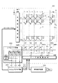
<1.第1実施形態>
図1は、本発明の第1実施形態に係る電気光学装置の電気的構成を示すブロック図であ
る。この電気光学装置は、電気光学物質として液晶を用いるものであり、液晶パネルAA
、タイミング発生回路400及び画像処理回路500を備える。液晶パネルAAは、薄膜
トランジスタ(Thin Film Transistor:以下、「TFT」と称する)、を形成した素子基
板と対向基板とを互いに電極形成面を対向させて、かつ、一定の間隙を保って貼付し、こ
の間隙に液晶が挟持されている。液晶パネルAAの素子基板上には、画像表示領域A、走
査線駆動回路100、データ線駆動回路200、レベルシフト回路300、及びデマルチ
プレクサDMP1〜DMPnが形成されている。
<1. First Embodiment>
FIG. 1 is a block diagram illustrating an electrical configuration of the electro-optical device according to the first embodiment of the invention. This electro-optical device uses liquid crystal as an electro-optical material, and has a liquid crystal panel AA.
The
この電気光学装置に供給される入力画像データDinは、例えば、3ビットパラレルの
形式である。タイミング発生回路400は、入力画像データDinに同期してYクロック
信号YCK、反転Yクロック信号YCKB、及びY転送開始パルスDYを生成して、走査
線駆動回路100に供給する。また、タイミング発生回路400は、入力画像データDi
nに同期してXクロック信号XCK、反転Xクロック信号XCKB、及びX転送開始パル
スDXを生成して、データ線駆動回路200に供給する。Y転送開始パルスDYは、垂直
走査周期のパルスであって、垂直走査期間の始まりから所定期間だけアクティブとなる。
一方、X転送開始パルスDXは、水平走査周期のパルスであって、水平走査期間の始まり
から所定期間だけアクティブとなる。
The input image data Din supplied to the electro-optical device has, for example, a 3-bit parallel format. The
In synchronization with n, an X clock signal XCK, an inverted X clock signal XCKB, and an X transfer start pulse DX are generated and supplied to the data line driving
On the other hand, the X transfer start pulse DX is a pulse having a horizontal scanning period and becomes active for a predetermined period from the start of the horizontal scanning period.
走査線駆動回路100は、シフトレジスタを備え、Y転送開始パルスDYを、Yクロッ
ク信号YCK及び反転Yクロック信号YCKBに同期して順次転送し、走査信号Y1、Y
2、…、Ymを順次生成する。
The scanning
2,..., Ym are sequentially generated.
画像処理回路500は、入力画像データDinに、液晶パネルAAの光透過特性を考慮
したガンマ補正等を施して出力画像データDoutを生成し、これをデータ線駆動回路2
00に供給する。データ線駆動回路200は、シフトレジスタ、ラッチ回路、及びDA変
換回路を備える。シフトレジスタは、X転送開始パルスDXを、Xクロック信号XCK及
び反転Yクロック信号YCKBに同期して順次転送し、ラッチパルスを生成する。ラッチ
回路は、ラッチパルスを用いて出力画像データDoutをラッチする。DA変換回路は、
ラッチ回路の出力信号をDA変換して、画像信号x1、x2、…、xnを各々生成する。
各画像信号x1、x2、…、xnにはR用、B用、G用の信号が時分割多重されている。
The
To 00. The data line driving
The output signal of the latch circuit is DA-converted to generate image signals x1, x2,.
Signals for R, B, and G are time-division multiplexed on each image signal x1, x2,..., Xn.
デマルチプレクサDMP1〜DMPnの各々は、TFTで構成される3個のスイッチS
W1、SW2、及びSW3を備える。スイッチSW1には高振幅選択信号RSEL’、ス
イッチSW2には高振幅選択信号GSEL’、スイッチSW3には高振幅選択信号BSE
L’が各々供給される。
Each of the demultiplexers DMP1 to DMPn includes three switches S composed of TFTs.
W1, SW2, and SW3 are provided. The switch SW1 has a high amplitude selection signal RSEL ′, the switch SW2 has a high amplitude selection signal GSEL ′, and the switch SW3 has a high amplitude selection signal BSE.
L ′ is supplied to each.
レベルシフト回路300は、低振幅選択信号RSEL、GSEL、及びBSELの信号
レベルを低振幅から高振幅に変換して、高振幅選択信号RSEL’、GSEL’、及びB
SEL’を各々生成する。低振幅選択信号RSEL、GSEL、及びBSELのLレベル
はVSSL、HレベルはVDDLであり、高振幅選択信号RSEL’、GSEL’、及び
BSEL’のLレベルはVSSH、HレベルはVDDHである。レベルシフト回路300
の詳細は後述する。
The
Each of SEL ′ is generated. The L level of the low amplitude selection signals RSEL, GSEL, and BSEL is VSSL and the H level is VDDL, and the L level of the high amplitude selection signals RSEL ′, GSEL ′, and BSEL ′ is VSSH, and the H level is VDDH.
Details will be described later.
次に、画像表示領域Aには、m(mは2以上の自然数)本の走査線2が、X方向に沿っ
て平行に配列して形成される一方、3n(nは2以上の自然数)本のデータ線3が、Y方
向に沿って平行に配列して形成されている。そして、走査線2とデータ線3との交差付近
においては、TFT50のゲートが走査線2に接続される一方、TFT50のソースがデ
ータ線3に接続されるとともに、TFT50のドレインが画素電極6に接続される。そし
て、各画素は、画素電極6と、対向基板に形成される対向電極と、これら両電極間に挟持
された液晶とによって構成される。この結果、走査線2とデータ線3との各交差に対応し
て、画素はマトリクス状に配列されることとなる。
Next, in the image display area A, m (m is a natural number of 2 or more)
また、TFT50のゲートが接続される各走査線2には、走査信号Y1、Y2、…、Y
mが、パルス的に線順次で印加されるようになっている。このため、ある走査線2に走査
信号が供給されると、当該走査線に接続されるTFT50がオンするので、データ線3か
ら所定のタイミングで供給されるデータ線信号X1、X2、…、X3nは、対応する画素
に順番に書き込まれた後、所定の期間保持されることとなる。
Further, each
m is applied in a pulse-sequential line-sequential manner. Therefore, when a scanning signal is supplied to a
各画素に印加される電位レベルに応じて液晶分子の配向や秩序が変化するので、光変調
による階調表示が可能となる。例えば、液晶を通過する光量は、ノーマリーホワイトモー
ドであれば、印加電位が高くなるにつれて制限される一方、ノーマリーブラックモードで
あれば、印加電位が高くなるにつれて緩和されるので、液晶表示装置全体では、画像信号
に応じたコントラストを持つ光が各画素毎に出射される。このため、所定の表示が可能と
なる。
Since the orientation and order of liquid crystal molecules change according to the potential level applied to each pixel, gradation display by light modulation becomes possible. For example, in the normally white mode, the amount of light passing through the liquid crystal is limited as the applied potential is increased. In the normally black mode, the amount of light is reduced as the applied potential is increased. As a whole, light having contrast according to the image signal is emitted for each pixel. For this reason, a predetermined display becomes possible.
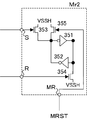
次に、レベルシフト回路300の詳細を説明する。図1に示すようにレベルシフト回路
300は、R用レベルシフタ321、G用レベルシフタ322、及びB用レベルシフタ3
23、並びにこれらの動作を制御する制御部310を備える。制御部310は、各レベル
シフタ321〜323の動作を制御する制御信号C1、C2、及びC3を生成する。
Next, details of the
23, and a
図2にレベルシフト回路300の詳細な構成を示す。G用レベルシフタ322及びB用
レベルシフタ323は、R用レベルシフタ321と同一の構成である。また、制御部31
0は、レベルシフタ321〜323に各々対応したR用メモリMr1、G用メモリMg1
、及びB用メモリMb1を備える。G用メモリMg1及びB用メモリMb1は、R用メモ
リMr1と同一の構成であり、セット端子Sとリセット端子Rを備える。これらのメモリ
は、対応するレベルシフタを各々制御する制御回路として機能する。
FIG. 2 shows a detailed configuration of the
0 is an R memory Mr1 and a G memory Mg1 corresponding to the
And B memory Mb1. The G memory Mg1 and the B memory Mb1 have the same configuration as the R memory Mr1, and include a set terminal S and a reset terminal R. These memories function as control circuits for controlling the corresponding level shifters.
R用レベルシフタ321において、コンデンサ(容量)331、332の一端には、低
振幅選択信号RSELが供給される。一方、コンデンサ331の他端は、Pチャネル型の
TFT341のゲートに、コンデンサ332の他端は、Nチャネル型のTFT342のゲ
ートに、それぞれ接続される。
In the
次に、TFT341のソースは、高位側電位VDDHの供給線に接続され、また、TFT
342のソースは、低位側電位VSSHの供給線に接続され、更に、TFT341及び12
4のドレインは共通接続されている。ここで、TFT341、342の共通ドレインをC
dと表記する。続いて、TFT341、342の共通ドレインCdは、インバータ343
の入力端子に接続される。インバータ343の出力端子から高振幅選択信号RSEL’が
出力される。
Next, the source of the
The source of 342 is connected to the supply line of the lower potential VSSH, and the
The drains of 4 are commonly connected. Here, the common drain of
Indicated as d. Subsequently, the common drain Cd of the
Connected to the input terminal. A high amplitude selection signal RSEL ′ is output from the output terminal of the
コンデンサ331の他端、すなわち、TFT341のゲートには、第1のオフセット回
路を構成するクロックドインバータ334によって、電圧Vofs1がオフセットされてい
る。同様に、コンデンサ332の他端(ゲートNin)には、第2のオフセット回路を構成
するクロックドインバータ335によって、電圧Vofs2がオフセットされる。電圧Vofs1
,及び電圧Vofs2はレベルシフタの出力状態に応じて変わる電位である。
The voltage Vofs1 is offset to the other end of the
, And the voltage Vofs2 are potentials that change according to the output state of the level shifter.
図3に、クロックドインバータ334及び335の回路図を示す。Nチャネル型のトラ
ンジスタN2には制御信号C1が供給される一方、Pチャネル型のトランジスタP2には
反転制御信号C1’が供給される。反転制御信号C1’は、インバータ336によって制
御信号C1を反転されたものである。従って、制御信号C1がアクティブになると、トラ
ンジスタP2及びN2がオン状態となり、クロックドインバータ334及び335が動作
して電流が流れる。一方、制御信号C1がアクティブになると、トランジスタP2及びN
2がオン状態となり、トランジスタP1及びN1が動作して貫通電流が流れる。一方、制
御信号C1が非アクティブになると、トランジスタP2及びN2がオフ状態となり、クロ
ックドインバータ334及び335の動作が停止するから、クロックドインバータ334
及び335における貫通電流が流れない。なお、制御信号C1がアクティブになると、図
2に示すTFT337及び339がオン状態となる。このため、TFT341、342のゲート端
子にはVSSHの電位が供給される。その結果共通ドレインCdはVDDHの電位となり、レベルシ
フタ321を構成する全てのTFTの貫通電流は流れない。
FIG. 3 shows a circuit diagram of the clocked
2 is turned on, the transistors P1 and N1 operate, and a through current flows. On the other hand, when the control signal C1 becomes inactive, the transistors P2 and N2 are turned off, and the operations of the clocked
And the through current at 335 does not flow. Note that when the control signal C1 becomes active, the
このように、クロックドインバータ334及び335、TFT337及び339は、制
御信号C1に基づいてレベル変換動作を実行するか否かを制御する機能を有する。レベル
変換動作を停止している期間は、R用レベルシフタ321は電力を消費しない。クロック
ドインバータ334及び335、TFT337及び339は、後述する制御部310と協
同して、R用レベルシフタ321の消費電力の削減に寄与する。
As described above, the clocked
低振幅選択信号RSELが長時間反転しないと、コンデンサ331及び332の一端に
おける微分波形の信号レベルは電圧Vofs1又はVofs2に収束していく。上述したように
、しきい値電圧VthPは、電圧Vofs1よりも低く設定され、しきい値電圧VthPは、電
圧Vofs1よりも低く設定される。したがって、TFT338及びTFT340を設けな
い回路では、低振幅選択信号RSELが長時間反転しないと、低振幅選択信号RSELの
論理レベルが遷移していないのに、高振幅選択信号RSEL’が反転することが起こりえ
る。TFT338及びTFT340はこのような誤動作を防止するために設けられている
。
If the low amplitude selection signal RSEL is not inverted for a long time, the signal level of the differential waveform at one end of the
低振幅選択信号RSELが低位側電位VSSLから高位側電位VDDLに遷移すると、その微
分波形の立ち上がりによってTFT341のゲート電位は、しきい値VthPを越えるので
TFT341がオフする一方、TFT342のゲート電位は、しきい値VthN以上となる
のでTFT342がオンする。このため、共通ドレインCdの電位は、Lレベルに相当す
る低位側電位VSSHとなる。よって、TFT340がオンする結果、TFT342のゲー
ト電位は、クロックドインバータ335によるオフセット電圧にかかわらず、高位側電位
VDDHに維持される。したがって、この後、低振幅選択信号RSELが長期間にわたって
高位側電位VDDLとなっても、TFT342のゲート電位は、しきい値VthNを下回るこ
とはない。一方、TFT338はオフであるので、TFT341のゲート電位は、低振幅
選択信号RSELの微分波形に電圧Vofs1をオフセットしたものとなる。
When the low amplitude selection signal RSEL transitions from the lower potential VSSL to the higher potential VDDL, the gate potential of the
また、低振幅選択信号RSELが高位側電位VDDLから低位側電位VSSLに遷移すると、
その微分波形の立ち下がりによってTFT341のゲート電位は、しきい値VthP以下と
なるのでTFT341がオンする。このため、共通ドレインCdの電位は、Hレベルに相
当する高位側電位VDDHとなる。よって、TFT338がオンする結果、TFT341の
ゲート電位は、クロックドインバータ334によるオフセット電圧にかかわらず、低位側
電位VSSHに維持される。したがって、この後、低振幅選択信号RSELが長期間にわた
って低位側電位VSSLとなっても、TFT341のゲート電位は、しきい値VthPを上回
ることはない。一方、TFT340はオフであるので、TFT342のゲート電位は、低
振幅選択信号RSELの微分波形に電圧Vofs2をオフセットしたものとなる。よって、
R用レベルシフタ321は、同一の論理レベルが長期間にわたる場合であっても、誤動作
することなく安定して動作する。
Further, when the low amplitude selection signal RSEL transitions from the higher potential VDDL to the lower potential VSSL,
Due to the fall of the differential waveform, the gate potential of the
The
次に、制御部310の一部であるR用メモリMr1について説明する。なお、G用メモ
リMg1及びB用メモリMb1は、R用メモリMr1と同様に構成されている。R用メモ
リMr1はインバータ351及び352によって構成されるラッチ回路と、TFT353
ならびにTFT354を備える。TFT353のゲートはセット端子Sに接続されている
。セット端子Sの信号レベルがHレベルになると、制御信号C1の論理レベルがHレベル
にセットされる。TFT354のゲートはリセット端子Rに接続されている。リセット端
子Rの信号レベルがHレベルになると、制御信号C1の論理レベルはLレベルにリセット
される。すなわち、R用メモリMr1は、SRフリップフロップ回路として機能する。
Next, the R memory Mr1 which is a part of the
In addition, a
上述したように低振幅選択信号は、RSEL→GSEL→BSEL→RSEL→GSE
L→BSEL…といったように、循環的にアクティブとなる。このように循環的にあくテ
ィティブとなる信号群の信号レベルを変換する場合には、常時、レベルシフタが動作する
必要はなく、対象となる信号がアクティブとなる期間にのみ動作すれば足りる。そこで、
制御部310は、ある低振幅選択信号が供給されるレベルシフタの動作を、当該低振幅選
択信号に先行する低振幅選択信号を用いて許可し、当該低振幅選択信号に後行する低振幅
選択信号を用いて禁止するように各制御信号を生成する。
As described above, the low amplitude selection signal is RSEL->GSEL->BSEL->RSEL-> GSE.
It becomes active cyclically, such as L → BSEL. Thus, when converting the signal level of the cyclically active signal group, it is not always necessary to operate the level shifter, and it is sufficient to operate only during a period in which the target signal is active. Therefore,
The
図4に、低振幅選択信号と制御信号のタイミングチャートを示す。R用メモリMr1の
セット端子Sには低振幅選択信号BSELが供給される一方、そのリセット端子Rには低
振幅選択信号GSELが供給される。したがって、時刻t3において低振幅選択信号BS
ELがアクティブになると、制御信号C1がHレベルとなり、その後、時刻t5において
低振幅選択信号GSELがアクティブになると、制御信号C1がLレベルとなる。この結
果、時刻t3から時刻t5までの期間T1において、制御信号C1がアクティブとなり、
R用レベルシフタが動作する。低振幅選択信号RSELがアクティブとなる期間T2は、
期間T1に含まれるため、R用レベルシフタ321は所期の目的を達成することができる
。
FIG. 4 shows a timing chart of the low amplitude selection signal and the control signal. The low amplitude selection signal BSEL is supplied to the set terminal S of the R memory Mr1, while the low amplitude selection signal GSEL is supplied to the reset terminal R thereof. Therefore, at time t3, the low amplitude selection signal BS
When EL becomes active, the control signal C1 becomes H level, and when the low amplitude selection signal GSEL becomes active at time t5, the control signal C1 becomes L level. As a result, in the period T1 from time t3 to time t5, the control signal C1 becomes active,
The R level shifter operates. The period T2 during which the low amplitude selection signal RSEL is active is
Since it is included in the period T1, the
一方、時刻t5から次に低振幅選択信号BSELがアクティブになる時刻t6までの期
間Trは、制御信号C1が非アクティブとなり、R用レベルシフタ231は動作を停止す
る。また、時刻t2から時刻t3の期間TrにおいてもR用レベルシフタ231は動作を
停止する。これらの期間Trにおいては貫通電流が「0」となるので、R用シフトレジス
タ321は、常時動作する場合と比較して、消費電力を2/3倍に削減することが可能と
なる。また、G用レベルシフタ322は期間Tgにおいて、B用レベルシフタ323は期
間Tbにおいて動作を停止するので、R用シフトレジスタ321と同様に、消費電力を2
/3倍に削減することが可能となる。
On the other hand, in the period Tr from time t5 to time t6 when the next low amplitude selection signal BSEL becomes active, the control signal C1 is inactive, and the R level shifter 231 stops its operation. Further, the R level shifter 231 also stops operating during the period Tr from time t2 to time t3. Since the through current is “0” during these periods Tr, the
/ 3 times as much as possible.
<2.第2実施形態>
図5は、本発明の第2実施形態に係る電気光学装置の主要部の電気的構成を示すブロッ
ク図である。この電気光学装置は、レベルシフト回路300の制御部310がマスターリ
セット信号MRSTでリセットされる点を除いて、第1実施形態の電気光学装置と同様に
構成されている。タイミング発生回路400は、電源投入の直後にアクティブとなるマス
ターリセット信号MRSTを生成する。なお、マスターリセット信号MRSTは、低振幅
選択信号RSEL、GSEL、及びBSELがアクティブとなる前にアクティブとなるこ
とが好ましい。
<2. Second Embodiment>
FIG. 5 is a block diagram showing the electrical configuration of the main part of the electro-optical device according to the second embodiment of the invention. This electro-optical device is configured in the same manner as the electro-optical device of the first embodiment, except that the
図6に、レベルシフト回路300の詳細な構成を示す。レベルシフタ321〜323は
、第1実施形態と同様に構成されている。一方、R用メモリMr2、G用メモリMg2、
及びB用メモリMb2はマスターリセット端子MRを備える点で第1実施形態の各メモリ
Mr1、Mg1、及びMb1と相違する。図7はR用メモリMr2の回路であり、図8は
G用メモリMg2及びB用メモリMb2の回路図である。まず、R用メモリMr2におい
ては、TFT353と並列にTFT355が追加されている。TFT355は、マスター
リセット端子MRの電位がHレベルになるとオン状態となり、制御信号C1をアクティブ
とする。一方、G用メモリMg2及びB用メモリMb2には、TFT354と並列にTF
T356が追加されている。TFT356は、マスターリセット端子MRの電位がHレベ
ルになるとオン状態となり、制御信号C1を非アクティブとする。
FIG. 6 shows a detailed configuration of the
And the memory for memory Mb2 are different from the memories Mr1, Mg1, and Mb1 of the first embodiment in that they include a master reset terminal MR. FIG. 7 is a circuit diagram of the R memory Mr2, and FIG. 8 is a circuit diagram of the G memory Mg2 and the B memory Mb2. First, in the R memory Mr2, a
T356 is added. The
上述した第1実施形態の制御部310において、各メモリMr1、Mg1、及びMb1
の初期状態は不定である。換言すれば、レベルシフタ321〜323に対して動作を許可
する制御信号C1〜C3を生成するとは限らない。このため、電源投入時において、制御
信号C1〜C3が総て非アクティブとなることがある。この場合、低振幅選択信号RSE
L、GSEL、BSELがアクティブになってもレベル変換は実行されない。もっとも、
1水平走査期間が経過すれば、各メモリMr1、Mg1、及びMb1のセット端子Sのレ
ベルが順次Hレベルとなるので、正常動作に復帰する。
In the
The initial state of is undefined. In other words, the control signals C1 to C3 that allow the
Even if L, GSEL, and BSEL become active, level conversion is not executed. However,
When one horizontal scanning period elapses, the level of the set terminal S of each of the memories Mr1, Mg1, and Mb1 sequentially becomes H level, so that normal operation is restored.
本実施形態によれば、マスターリセット信号MRSTを制御部310に供給する。する
と、R用メモリMr2においては、その記憶内容が動作許可状態にセットされ、G用メモ
リMg2及びB用メモリMb2においてはそれらの記憶内容が動作禁止状態にリセットさ
れる。この例では、電源投入の後に最初にアクティブとなる低振幅選択信号はRSELで
ある。従って、電源投入の直後であっても、レベルシフタ321〜323を安定して動作
させることが可能となる。この結果、表示画像の乱れを無くすことが可能となる。
According to the present embodiment, the master reset signal MRST is supplied to the
なお、マスターリセット信号MRSTとして、Y転送開始パルスDYを供給してもよい
。上述したようにY転送開始パルスDYは、垂直走査期間の始まりでアクティブとなる。
また、低振幅選択信号RSEL、GSEL、及びBSELは、各垂直走査期間においてY
転送開始パルスDYのアクティブ期間が終了した後にアクティブとなる。従って、Y転送
開始パルスDYをマスターリセット信号MRSTとして用いることによって、安定して動
作させることができる。更に、タイミング発生回路400はY転送開始パルスDYと独立
してマスターリセット信号MRSTを生成する必要がないので、タイミング発生回路40
0の構成を簡易にできる。また、マスターリセット信号MRSTとして、X転送開始パル
スDXを用いてもよい。X転送開始パルスDXは水平走査期間の始まりでアクティブとな
る信号であるが、各水平走査期間においてX転送開始パルスDXが非アクティブとなった
後、低振幅選択信号RSEL、GSEL、及びBSELはアクティブとなる。従って、X
転送開始パルスDXをマスターリセット信号MRSTとして用いても、安定して動作させ
ることができ、タイミング発生回路400の構成を簡易にできる。
Note that the Y transfer start pulse DY may be supplied as the master reset signal MRST. As described above, the Y transfer start pulse DY becomes active at the beginning of the vertical scanning period.
In addition, the low amplitude selection signals RSEL, GSEL, and BSEL are Y in each vertical scanning period.
It becomes active after the active period of the transfer start pulse DY ends. Therefore, stable operation can be achieved by using the Y transfer start pulse DY as the master reset signal MRST. Furthermore, since the
The configuration of 0 can be simplified. Further, an X transfer start pulse DX may be used as the master reset signal MRST. The X transfer start pulse DX is an active signal at the beginning of the horizontal scanning period, but the low amplitude selection signals RSEL, GSEL, and BSEL are active after the X transfer start pulse DX becomes inactive in each horizontal scanning period. It becomes. Therefore, X
Even if the transfer start pulse DX is used as the master reset signal MRST, it can be operated stably, and the configuration of the
<3.応用例>
(1)上述した第1及び第2実施形態において、制御部310は、低振幅選択信号RS
EL、GSEL、及びBSELに基づいて制御信号C1〜C3を生成したが、高振幅選択
信号RSEL’、GSEL’、及びBSEL’に基づいて制御信号C1〜C3を生成して
もよい。例えば、図1に示す第1実施形態の電気光学装置において、レベルシフト回路3
00の代わりに図9に示すレベルシフト回路300Aを用いてもよい。また、図5に示す
第2実施形態の電気光学装置において、レベルシフト回路300の代わりに図10に示す
レベルシフト回路300Bを用いてもよい。
<3. Application example>
(1) In the first and second embodiments described above, the
Although the control signals C1 to C3 are generated based on EL, GSEL, and BSEL, the control signals C1 to C3 may be generated based on the high amplitude selection signals RSEL ′, GSEL ′, and BSEL ′. For example, in the electro-optical device according to the first embodiment shown in FIG.
Instead of 00, a
(2)上述した第1及び第2実施形態、並びに応用例では、デマルチプレクサDMP1
〜DMPnとして1入力3出力のものを用いたが、その倍率は、3以上であれば任意であ
る。データ線駆動回路200を液晶パネルAAの外部に設ける場合には、画像信号x1、
x2、…を供給するために液晶パネルAAの端部に入力端子を設ける必要がある。そのよ
うな構成においては、入力端子間の短絡を防止するため入力端子数を低減することが重要
である。この場合、デマルチプレクサの倍率を上げるのが有効である。しかしながら、デ
マルチプレクサの倍率を上げると、選択信号の数が増加するので、レベルシフタの数も増
加して消費電力が増える。上述したレベルシフト回路は、選択信号の数が増加する程、消
費電力を削減することができる。
(2) In the first and second embodiments and application examples described above, the demultiplexer DMP1
Although 1
In order to supply x2,..., it is necessary to provide an input terminal at the end of the liquid crystal panel AA. In such a configuration, it is important to reduce the number of input terminals in order to prevent a short circuit between the input terminals. In this case, it is effective to increase the magnification of the demultiplexer. However, if the magnification of the demultiplexer is increased, the number of selection signals increases, so the number of level shifters also increases and power consumption increases. The level shift circuit described above can reduce power consumption as the number of selection signals increases.
例えば、1入力6出力のデマルチプレクサを用いる場合を想定する。図11は、1入力
6出力のデマルチプレクサに対応するレベルシフト回路300Cのブロックである。同図
に示すメモリM1〜M6は、図2に示すR用メモリMr1と同様の構成であり、レベルシ
フタ361〜366は、図2に示すR用レベルシフタ321と同様の構成である。
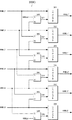
For example, assume that a 1-input 6-output demultiplexer is used. FIG. 11 is a block diagram of a
図12に、レベルシフト回路300Cのタイミングチャートを示す。この図に示すよう
に低振幅選択信号は、RSEL1→GSEL1→BSEL1→RSEL2→GSEL2→
BSEL2の順にアクティブとなり、このサイクルを繰り返する。ここで、レベルシフタ
332に着目すると、レベルシフタ332に対応するメモリM2のセット端子Sには低振
幅信号RSEL1が供給され、リセット端子Rには低振幅選択信号BSEL1が供給され
ている。従って、制御信号C2は、時刻t1において低振幅選択信号RSEL1がHレベ
ルになるとアクティブとなり、時刻t3において低振幅選択信号BSEL1がHレベルに
なると非アクティブになる。そして、時刻t2において再び低振幅選択信号RSEL1が
アクティブになるまで、制御信号C2は非アクティブとなる。制御信号C2が非アクティ
ブとなる期間は、レベルシフタ332の動作が停止して貫通電流が「0」となる。従って
、レベルシフタ332の消費電力は、常時動作する場合と比較して1/3倍に低減される
。
FIG. 12 shows a timing chart of the
It becomes active in the order of BSEL2, and this cycle is repeated. Here, paying attention to the
この例では、ある低振幅選択信号(例えば、GSEL1)がアクティブとなるタイミン
グの直前にアクティブとなる低振幅選択信号(例えば、RSEL1)を用いてメモリに動
作許可状態を記憶し、直後にアクティブとなる低振幅選択信号(例えば、BSEL1)用
いてメモリに動作禁止状態を記憶し、メモリの記憶内容に従ってある低振幅選択信号が供
給されるレベルシフタの動作が制御される。なお、直前、直後の低振幅選択信号の代わり
に2つ前、2つ後にアクティブとなる低振幅選択信号を用いて、メモリの記憶内容を書き
換えてもよい。要は、ある低振幅選択信号に先行してアクティブとなる先行選択信号を用
いてメモリに動作許可状態を記憶し、後行する後行選択信号を用いてメモリに動作禁止状
態を記憶し、メモリの記憶内容に従ってある低振幅選択信号が供給されるレベルシフタの
動作を制御すればよい。もっとも、直前、直後の低振幅選択信号を用いる場合が消費電力
の低減効果が最大であり。2つ前、2つ後にアクティブとなる低振幅選択信号を用いると
、貫通電流の停止期間が短くなるので消費電力の低減効果が減少する。
In this example, an operation permission state is stored in the memory using a low amplitude selection signal (for example, RSEL1) that becomes active immediately before a timing at which a certain low amplitude selection signal (for example, GSEL1) becomes active. The low-amplitude selection signal (for example, BSEL1) is used to store the operation prohibited state in the memory, and the operation of the level shifter to which a certain low-amplitude selection signal is supplied is controlled according to the stored contents of the memory. Note that the stored contents of the memory may be rewritten using a low amplitude selection signal that becomes active two before and after two instead of the immediately preceding and immediately following low amplitude selection signals. In short, an operation enabling state is stored in the memory using a preceding selection signal that becomes active prior to a certain low amplitude selection signal, and an operation prohibiting state is stored in the memory using a succeeding selection signal that follows. The operation of the level shifter to which a certain low amplitude selection signal is supplied may be controlled in accordance with the stored contents. However, the effect of reducing power consumption is greatest when the immediately preceding and immediately following low amplitude selection signals are used. When a low-amplitude selection signal that becomes active two times before and after two is used, the stop period of the through current is shortened, so that the effect of reducing power consumption is reduced.
また、この応用例においても、メモリM1〜M6として上述したマスターリセット端子
を備えたものを用いてもよく、この場合には、マスターリセット信号MRSTとしてY転
送開始パルスDY又はX転送開始パルスDXを用いてもよい。更に、上述した応用例と同
様に、メモリM1〜M6のセット端子S及びリセット端子Rに、高選択振幅信号を供給し
てもよい。
Also in this application example, the memories M1 to M6 having the above-described master reset terminal may be used. In this case, the Y transfer start pulse DY or the X transfer start pulse DX is used as the master reset signal MRST. It may be used. Further, similarly to the application example described above, a high selection amplitude signal may be supplied to the set terminal S and the reset terminal R of the memories M1 to M6.
<4.電子機器>
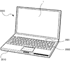
次に、本発明に係る電気光学装置を適用した電子機器について説明する。図13に、上
記各実施形態に係る電気光学装置を適用したモバイル型のパーソナルコンピュータの構成
を示す。パーソナルコンピュータ2000は、表示ユニットとしての電気光学装置1と本
体部2010を備える。本体部2010には、電源スイッチ2001及びキーボード20
02が設けられている。この電気光学装置は低消費電力で動作する。
<4. Electronic equipment>
Next, an electronic apparatus to which the electro-optical device according to the invention is applied will be described. FIG. 13 shows a configuration of a mobile personal computer to which the electro-optical device according to each of the above embodiments is applied. The
02 is provided. This electro-optical device operates with low power consumption.
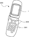
図14に、上記各実施形態に係る電気光学装置を適用した携帯電話機の構成を示す。携
帯電話機3000は、複数の操作ボタン3001及びスクロールボタン3002、ならび
に表示ユニットとしての電気光学装置を備える。スクロールボタン3002を操作するこ
とによって、電気光学装置に表示される画面がスクロールされる。この携帯電話機300
0によれば、電気光学装置の消費電力が削減されているので、1回の充電で長時間動作さ
せることが可能となる。
FIG. 14 shows a configuration of a mobile phone to which the electro-optical device according to each of the above embodiments is applied. A
According to 0, since the power consumption of the electro-optical device is reduced, it is possible to operate for a long time with one charge.
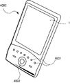
図15に、上記各実施形態に係る電気光学装置を適用した情報携帯端末(PDA:Pers
onal Digital Assistants)の構成を示す。情報携帯端末4000は、複数の操作ボタン
4001及び電源スイッチ4002、ならびに表示ユニットとしての電気光学装置を備え
る。電源スイッチ4002を操作すると、住所録やスケジュール帳といった各種の情報が
電気光学装置に表示される。
FIG. 15 shows a portable information terminal (PDA: Pers) to which the electro-optical device according to each of the above embodiments is applied.
onal Digital Assistants). The
なお、本発明に係る電気光学装置が適用される電子機器としては、図13から図15に
示したもののほか、デジタルスチルカメラ、液晶テレビ、ビューファインダ型、モニタ直
視型のビデオテープレコーダ、カーナビゲーション装置、ページャ、電子手帳、電卓、ワ
ードプロセッサ、ワークステーション、テレビ電話、POS端末、タッチパネルを備えた
機器等などが挙げられる。
The electronic apparatus to which the electro-optical device according to the present invention is applied includes those shown in FIGS. 13 to 15, a digital still camera, a liquid crystal television, a viewfinder type, a monitor direct view type video tape recorder, a car navigation system. Examples thereof include a device, a pager, an electronic notebook, a calculator, a word processor, a workstation, a videophone, a POS terminal, and a device equipped with a touch panel.
2…走査線、3…データ線、100…走査線駆動回路、200…データ線駆動回路、3
00…レベルシフト回路、310…制御部、321〜323…レベルシフタ、Mr1…R
用メモリ、Mg1…G用メモリ、Mb1…B用メモリ、C1〜C6…制御信号、DMP1
〜DMPn…デマルチプレクサ、RSEL、GSEL、BSEL…低振幅選択信号、
RSEL’、GSEL’、BSEL’…低振幅選択信号。
2 ... scanning line, 3 ... data line, 100 ... scanning line driving circuit, 200 ... data line driving circuit, 3
00 ... Level shift circuit, 310 ... Control unit, 321-323 ... Level shifter, Mr1 ... R
Memory, Mg1 ... G memory, Mb1 ... B memory, C1-C6 ... control signal, DMP1
~ DMPn ... demultiplexer, RSEL, GSEL, BSEL ... low amplitude selection signal,
RSEL ′, GSEL ′, BSEL ′... Low amplitude selection signal.
Claims (14)
(2),…,SEL(N)(ただし、Nは正の整数)が各々供給され、前記選択信号の信
号レベルを変換して各々出力する複数のレベルシフタと、
前記複数のレベルシフタの各々へ動作状態を制御する制御信号を供給する複数の制御回
路と、
を備え、
前記複数の選択信号SEL(1),SEL(2),…,SEL(N)は、そのうちの選
択信号SEL(N)がアクティブとなった後には選択信号SEL(1)がアクティブとな
るというが如く、その番号1,2,…,Nについて円環的にアクティブとなり、
前記複数の制御回路の各々は、
対応するレベルシフタに供給される選択信号SEL(t)(ただし、tは、1,2,…
,Nのいずれか)がアクティブとなる前にアクティブとなる先行選択信号SEL(t−1
)(ただし、t=1のときは、この(t−1)はNとする。)を用いて動作許可状態を指
示する前記制御信号を生成し、
前記選択信号SEL(t)がアクティブとなった後にアクティブとなる後行選択信号S
EL(t+1)(ただし、t=Nのときは、この(t+1)は1とする。)を用いて対応
する動作禁止状態を指示する前記制御信号を生成して、
当該制御信号を、対応するレベルシフタに供給することにより、
当該レベルシフタの動作許可及び動作禁止を、前記選択信号SEL(1),SEL(2
),…,SEL(N)のみを用いて行う、
ことを特徴とするレベルシフト回路。 Sequentially along the time axis, exclusively the active plurality of selection signals SEL (1), SEL
(2),..., SEL (N) (where N is a positive integer) , a plurality of level shifters for converting the signal level of the selection signal and outputting each of the level shifters;
A plurality of control circuits for supplying a control signal for controlling an operation state to each of the plurality of level shifters;
With
The plurality of selection signals SEL (1), SEL (2), ..., SEL (N) are selected from among them.
After the selection signal SEL (N) becomes active, the selection signal SEL (1) becomes active.
As you can see, the numbers 1, 2,...
Each of the plurality of control circuits includes:
Selection signal SEL (t) supplied to the corresponding level shifter (where t is 1, 2,...
, N) becomes a pre-selection signal SEL (t−1 ) that becomes active before it becomes active.
) (However, when t = 1, this (t−1) is N.) is used to generate the control signal indicating the operation permission state,
Subsequent selection signal S that becomes active after the selection signal SEL (t) becomes active
EL (t + 1) (however, when t = N, this (t + 1) is set to 1) to generate the control signal indicating the corresponding operation inhibition state,
By supplying the control signal to the corresponding level shifter ,
The selection signal SEL (1), SEL (2) is used to enable or disable the operation of the level shifter.
), ..., using only SEL (N),
A level shift circuit characterized by that.
アクティブとなる直前にアクティブとなり、前記後行選択信号SEL(t+1)は、対応
するレベルシフタに供給される選択信号がアクティブとなる直後にアクティブとなること
を特徴とする請求項1に記載のレベルシフト回路。 The preceding selection signal SEL (t−1) becomes active immediately before the selection signal supplied to the corresponding level shifter becomes active, and the subsequent selection signal SEL (t + 1) becomes the selection signal supplied to the corresponding level shifter. 2. The level shift circuit according to claim 1, wherein the level shift circuit becomes active immediately after the becomes active.
て又は加えて、
前記レベルシフタから出力される選択信号SEL’(1),SEL’(2),…,SE
L’(N)を用いて前記制御信号を生成することを特徴とする請求項1又は2に記載のレ
ベルシフト回路。 The control circuit replaces the selection signals SEL (1), SEL (2),..., SEL (N).
Or in addition,
Selection signal SEL output from the level shifter '(1), SEL' ( 2), ..., SE
The level shift circuit according to claim 1, wherein the control signal is generated using L ′ (N) .
前記メモリ回路は、前記先行選択信号SEL(t−1)がアクティブになると動作許可
状態を記憶し、前記後行選択信号SEL(t+1)がアクティブになると動作禁止状態を
記憶し、記憶内容に応じた信号を前記制御信号として出力する、
ことを特徴とする請求項1乃至3のうちいずれか1項に記載のレベルシフト回路。 The control circuit includes a memory circuit that stores an operation state;
The memory circuit stores an operation permission state when the preceding selection signal SEL (t−1) becomes active , and stores an operation prohibition state when the succeeding row selection signal SEL (t + 1) becomes active. Output the control signal as the control signal,
The level shift circuit according to any one of claims 1 to 3 , wherein the level shift circuit is configured as described above.
ベルを変換して各々出力する複数のレベルシフタと、
前記複数のレベルシフタの各々へ動作状態を制御する制御信号を供給する複数の制御回
路と、
を備え、
前記複数の制御回路の各々は、対応するレベルシフタに供給される選択信号がアクティ
ブとなる前にアクティブとなる先行選択信号を用いて動作許可状態を指示する前記制御信
号を生成し、前記選択信号がアクティブとなった後にアクティブとなる後行選択信号を用
いて対応する動作禁止状態を指示する前記制御信号を生成して、対応するレベルシフタに
供給し、
更に、
前記制御回路は動作状態を記憶するメモリ回路を備え、
前記メモリ回路は、前記先行選択信号がアクティブになると動作許可状態を記憶し、前
記後行選択信号がアクティブになると動作禁止状態を記憶し、記憶内容に応じた信号を前
記制御信号として出力し、
更に、
複数のメモリ回路のうち、所定のメモリ回路の記憶内容を動作許可状態にセットし、他
のメモリ回路の記憶内容を動作禁止状態にリセットする初期化動作を実行する初期化手段
を備えた、
ことを特徴とするレベルシフト回路。 A plurality of selection signals that are sequentially activated exclusively are supplied, and the signal level of the selection signal is supplied.
A plurality of level shifters that convert the bell and output each;
A plurality of control circuits for supplying a control signal for controlling an operation state to each of the plurality of level shifters.
Road,
With
In each of the plurality of control circuits, a selection signal supplied to a corresponding level shifter is activated.
The control signal for instructing the operation permission state using a preceding selection signal that becomes active before becoming
And a subsequent selection signal that becomes active after the selection signal becomes active is used.
The control signal for instructing the corresponding operation prohibition state is generated, and the corresponding level shifter is generated.
Supply
Furthermore,
The control circuit includes a memory circuit that stores an operation state;
The memory circuit stores an operation permission state when the preceding selection signal becomes active,
When the subsequent row selection signal becomes active, the operation prohibited state is stored, and the signal corresponding to the stored content is
Output as a control signal,
Furthermore,
Among the plurality of memory circuits, comprising an initialization means for performing an initialization operation of resetting the stored content of a predetermined memory circuit to set the operation enable state, the stored contents of the other memory circuits to the operation inhibition state,
Features and, Relais Berushifuto circuits that.
直前にアクティブとなり、前記後行選択信号は、対応するレベルシフタに供給される選択
信号がアクティブとなる直後にアクティブとなることを特徴とする請求項5に記載のレベ
ルシフト回路。 The preceding selection signal becomes active immediately before the selection signal supplied to the corresponding level shifter becomes active, and the subsequent selection signal becomes active immediately after the selection signal supplied to the corresponding level shifter becomes active. The level shift circuit according to claim 5 .
することを特徴とする請求項5又は6に記載のレベルシフト回路。 Wherein the control circuit, a level shift circuit according to claim 5 or 6, characterized in that to generate the control signals using the selection signal supplied to the level shifter.
成することを特徴とする請求項5又は6に記載のレベルシフト回路。 Wherein the control circuit, a level shift circuit according to claim 5 or 6, characterized in that to generate the control signals using the selection signal output from the level shifter.
複数の走査線と、
複数のデータ線と、
前記走査線と前記データ線との交差に対応して設けられた複数の電気光学素子と、
前記複数の走査線に走査信号を各々供給する走査線駆動回路と、
前記複数のデータ線に供給するデータ信号を生成するデータ線駆動回路と、
所定数のデータ線ごとに設けられた複数のデマルチプレクス回路と、
前記レベルシフト回路へ供給する前記複数の選択信号を生成するタイミング発生手段と
を備え、
前記複数のデマルチプレクス回路の各々は、前記レベルシフト回路から出力される複数
の選択信号に基づいて前記所定数のデータ線の中から選択した一のデータ線へ前記データ
信号を出力し、
前記タイミング発生手段は、電源が投入されてから前記複数の選択信号を生成する前に
初期化信号を生成して前記初期化手段に供給し、
前記初期化手段は前記初期化信号に従って前記初期化動作を実行する、
ことを特徴とする電気光学装置。 A level shift circuit according to any one of claims 5 to 8 ,
A plurality of scan lines;
Multiple data lines,
A plurality of electro-optic elements provided corresponding to the intersections of the scanning lines and the data lines;
A scanning line driving circuit for supplying a scanning signal to each of the plurality of scanning lines;
A data line driving circuit for generating a data signal to be supplied to the plurality of data lines;
A plurality of demultiplexing circuits provided for each predetermined number of data lines;
Timing generating means for generating the plurality of selection signals to be supplied to the level shift circuit,
Each of the plurality of demultiplexing circuits outputs the data signal to one data line selected from the predetermined number of data lines based on a plurality of selection signals output from the level shift circuit,
The timing generation unit generates an initialization signal before supplying the plurality of selection signals after power is turned on, and supplies the initialization signal to the initialization unit.
The initialization means executes the initialization operation in accordance with the initialization signal;
An electro-optical device.
生成して前記走査線駆動回路へ供給し、水平走査期間の始まりでアクティブとなる第2開
始信号を生成してデータ線駆動回路へ供給し、前記初期化信号を生成して前記初期化手段
へ供給する代わりに前記第1開始信号又は第2開始信号を前記初期化手段へ供給し、
前記初期化手段は、前記タイミング発生手段から供給される前記第1開始信号又は前記
第2開始信号に従って前記初期化動作を実行する、
ことを特徴とする請求項9に記載の電気光学装置。 The timing generating means generates a first start signal that becomes active at the start of a vertical scanning period, supplies the first start signal to the scanning line driving circuit, and generates a second start signal that becomes active at the start of a horizontal scanning period to generate data. Instead of supplying to the line drive circuit, generating the initialization signal and supplying it to the initialization means, supplying the first start signal or the second start signal to the initialization means;
The initialization unit executes the initialization operation according to the first start signal or the second start signal supplied from the timing generation unit.
The electro-optical device according to claim 9 .
入力信号の信号レベルを変換して出力信号を出力するレベルシフタであって、
前記入力信号が一端に供給される第1容量素子と、
一端が前記第1容量素子の一端と接続される第2容量素子と、
ゲートが前記第1容量素子の他端と接続され、ソースが高電位供給線と接続される第1
トランジスタと、
ゲートが前記第2容量素子の他端と接続され、ソースが低電位供給線と接続され、前記
ドレインが第1トランジスタのドレインと接続される第2トランジスタと、
前記高電位供給線と前記低電位供給線から電源が供給され、前記制御信号に基づいて前
記電源の供給を受けるか否かが制御され、入力端と出力端とが前記第1トランジスタのゲ
ートと接続される第1クロックドインバータと、
前記高電位供給線と前記低電位供給線から電源が供給され、前記制御信号に基づいて前
記電源の供給を受けるか否かが制御され、入力端と出力端が前記第2トランジスタのゲー
トと接続される第2クロックドインバータと、
前記第1トランジスタ及び前記第2トランジスタのドレインと入力端が接続され、出力
端から前記出力信号を出力するインバータとを、
備えたレベルシフタである、
ことを特徴とする請求項1乃至8のいずれか一項に記載のレベルシフト回路。 The level shifter is
A level shifter that converts the signal level of an input signal and outputs an output signal,
A first capacitor to which the input signal is supplied to one end;
A second capacitive element having one end connected to one end of the first capacitive element;
A first gate connected to the other end of the first capacitive element and a source connected to a high potential supply line.
A transistor,
A second transistor having a gate connected to the other end of the second capacitor, a source connected to a low potential supply line, and a drain connected to the drain of the first transistor;
Said high the potential supply line power from the low potential supply line is supplied, the control signal whether supplied with the power supply based on is controlled, and the gate of the input end and the output end of the first transistor A first clocked inverter connected;
Said high the potential supply line power from the low potential supply line is supplied, the control whether supplied with the power supply on the basis of a signal is controlled, connected to the input and output terminals and a gate of said second transistor A second clocked inverter,
An inverter connected to a drain and an input terminal of the first transistor and the second transistor and outputting the output signal from an output terminal;
It is a level shifter with
The level shift circuit according to any one of claims 1 to 8, wherein the level shift circuit is configured as described above .
複数の走査線と、
複数のデータ線と、
前記走査線と前記データ線との交差に対応して設けられた複数の電気光学素子と、
前記複数の走査線に走査信号を各々供給する走査線駆動回路と、
前記複数のデータ線に供給するデータ信号を生成するデータ線駆動回路と、
所定数のデータ線ごとに設けられた複数のデマルチプレクス回路とを備え、
前記複数のデマルチプレクス回路の各々は、前記レベルシフト回路から出力される複数
の選択信号に基づいて前記所定数のデータ線の中から選択した一のデータ線へ前記データ
信号を出力する、
ことを特徴とする電気光学装置。 A level shift circuit according to any one of claims 1 to 4 ,
A plurality of scan lines;
Multiple data lines,
A plurality of electro-optic elements provided corresponding to the intersections of the scanning lines and the data lines;
A scanning line driving circuit for supplying a scanning signal to each of the plurality of scanning lines;
A data line driving circuit for generating a data signal to be supplied to the plurality of data lines;
A plurality of demultiplexing circuits provided for each predetermined number of data lines,
Each of the plurality of demultiplexing circuits outputs the data signal to one data line selected from the predetermined number of data lines based on a plurality of selection signals output from the level shift circuit.
An electro-optical device.
Priority Applications (6)
| Application Number | Priority Date | Filing Date | Title |
|---|---|---|---|
| JP2004109223A JP4127232B2 (en) | 2004-04-01 | 2004-04-01 | Level shifter, level shift circuit, electro-optical device, and electronic apparatus |
| KR1020050020911A KR100714817B1 (en) | 2004-04-01 | 2005-03-14 | Level shifter, level shift circuit, electro-optical device, and electronic apparatus |
| US11/079,555 US7136311B2 (en) | 2004-04-01 | 2005-03-15 | Level shifter, level shift circuit, electro-optical device, and electronic apparatus |
| EP05006871A EP1585103A2 (en) | 2004-04-01 | 2005-03-30 | Level shifter, level shift circuit, electro-optical device, and electronic apparatus |
| TW094110345A TW200604981A (en) | 2004-04-01 | 2005-03-31 | Level shifter, level shift circuit, electro-optical device, and electronic apparatus |
| CNB2005100626105A CN100525106C (en) | 2004-04-01 | 2005-04-01 | Level shifter, level shift circuit, electro-optical device, and electronic apparatus |
Applications Claiming Priority (1)
| Application Number | Priority Date | Filing Date | Title |
|---|---|---|---|
| JP2004109223A JP4127232B2 (en) | 2004-04-01 | 2004-04-01 | Level shifter, level shift circuit, electro-optical device, and electronic apparatus |
Publications (2)
| Publication Number | Publication Date |
|---|---|
| JP2005292588A JP2005292588A (en) | 2005-10-20 |
| JP4127232B2 true JP4127232B2 (en) | 2008-07-30 |
Family
ID=34909461
Family Applications (1)
| Application Number | Title | Priority Date | Filing Date |
|---|---|---|---|
| JP2004109223A Expired - Lifetime JP4127232B2 (en) | 2004-04-01 | 2004-04-01 | Level shifter, level shift circuit, electro-optical device, and electronic apparatus |
Country Status (6)
| Country | Link |
|---|---|
| US (1) | US7136311B2 (en) |
| EP (1) | EP1585103A2 (en) |
| JP (1) | JP4127232B2 (en) |
| KR (1) | KR100714817B1 (en) |
| CN (1) | CN100525106C (en) |
| TW (1) | TW200604981A (en) |
Families Citing this family (13)
| Publication number | Priority date | Publication date | Assignee | Title |
|---|---|---|---|---|
| TWI344625B (en) * | 2005-03-08 | 2011-07-01 | Epson Imaging Devices Corp | Driving circuit of display device, driving circuit of electro-optical device, and electronic apparatus |
| US7830176B2 (en) * | 2006-07-27 | 2010-11-09 | Arm Limited | Controlling signal levels on a signal line within an integrated circuit |
| US20080117190A1 (en) * | 2006-11-22 | 2008-05-22 | Chien-Ru Chen | Method and driver for driving a display |
| KR20090050730A (en) * | 2007-11-16 | 2009-05-20 | 삼성전자주식회사 | Display device and control method of the same |
| JP4674280B2 (en) * | 2008-03-13 | 2011-04-20 | 奇美電子股▲ふん▼有限公司 | Demultiplexer, electronic device using the same, and liquid crystal display device |
| US9270273B2 (en) | 2011-10-28 | 2016-02-23 | Texas Instruments Incorporated | Level shifter |
| US8988960B2 (en) * | 2012-11-29 | 2015-03-24 | Nvidia Corporation | Technique for improving static random-access memory sense amplifier voltage differential |
| JP2014179723A (en) * | 2013-03-14 | 2014-09-25 | Seiko Epson Corp | Level shift circuit, electro-optical device and electronic apparatus |
| CN104253607B (en) * | 2013-06-25 | 2018-01-23 | 英业达科技有限公司 | Level adjusting circuit |
| US9607539B2 (en) * | 2014-12-31 | 2017-03-28 | Shenzhen China Star Optoelectronics Technology Co., Ltd. | Display panel capable of reducing a voltage level changing frequency of a select signal and drive circuit thereof |
| DE102016109118A1 (en) | 2016-05-18 | 2017-11-23 | Infineon Technologies Ag | Circuit architecture for a measuring device, a level converter circuit, a charge pumping stage and a charge pump and method for operating these |
| DE102016109114A1 (en) * | 2016-05-18 | 2017-11-23 | Infineon Technologies Ag | Circuit architecture for a measuring device, a level converter circuit, a charge pumping stage and a charge pump and method for operating these |
| JP6757352B2 (en) * | 2018-03-28 | 2020-09-16 | シャープ株式会社 | Active matrix board and display device |
Family Cites Families (15)
| Publication number | Priority date | Publication date | Assignee | Title |
|---|---|---|---|---|
| TW423162B (en) * | 1997-02-27 | 2001-02-21 | Toshiba Corp | Power voltage supplying circuit and semiconductor memory including the same |
| JPH11220380A (en) | 1998-02-03 | 1999-08-10 | Sony Corp | Level shift circuit |
| JP3858486B2 (en) * | 1998-11-26 | 2006-12-13 | セイコーエプソン株式会社 | Shift register circuit, electro-optical device and electronic apparatus |
| JP3473745B2 (en) * | 1999-05-28 | 2003-12-08 | シャープ株式会社 | Shift register and image display device using the same |
| JP3426541B2 (en) * | 1999-07-29 | 2003-07-14 | 株式会社 沖マイクロデザイン | Precharge control signal generation circuit |
| JP3588033B2 (en) * | 2000-04-18 | 2004-11-10 | シャープ株式会社 | Shift register and image display device having the same |
| JP2002175036A (en) * | 2000-12-07 | 2002-06-21 | Sanyo Electric Co Ltd | Active matrix display |
| JP3972735B2 (en) | 2001-06-26 | 2007-09-05 | セイコーエプソン株式会社 | Level shifter and electro-optical device using the same |
| JP3596540B2 (en) | 2001-06-26 | 2004-12-02 | セイコーエプソン株式会社 | Level shifter and electro-optical device using the same |
| TWI248056B (en) * | 2001-10-19 | 2006-01-21 | Sony Corp | Level converter circuits, display device and portable terminal device |
| JP3813538B2 (en) * | 2001-11-28 | 2006-08-23 | 富士通株式会社 | Level shifter |
| JP3791452B2 (en) * | 2002-05-02 | 2006-06-28 | ソニー株式会社 | Display device, driving method thereof, and portable terminal device |
| JP2004021096A (en) * | 2002-06-19 | 2004-01-22 | Sanyo Electric Co Ltd | Active matrix type display device |
| KR100432652B1 (en) | 2002-08-01 | 2004-05-22 | 삼성에스디아이 주식회사 | Level shifter and flat panel display |
| JP4326215B2 (en) | 2002-12-26 | 2009-09-02 | 株式会社 日立ディスプレイズ | Display device |
-
2004
- 2004-04-01 JP JP2004109223A patent/JP4127232B2/en not_active Expired - Lifetime
-
2005
- 2005-03-14 KR KR1020050020911A patent/KR100714817B1/en active IP Right Grant
- 2005-03-15 US US11/079,555 patent/US7136311B2/en active Active
- 2005-03-30 EP EP05006871A patent/EP1585103A2/en not_active Withdrawn
- 2005-03-31 TW TW094110345A patent/TW200604981A/en unknown
- 2005-04-01 CN CNB2005100626105A patent/CN100525106C/en active Active
Also Published As
| Publication number | Publication date |
|---|---|
| CN100525106C (en) | 2009-08-05 |
| JP2005292588A (en) | 2005-10-20 |
| KR20060043600A (en) | 2006-05-15 |
| EP1585103A2 (en) | 2005-10-12 |
| US7136311B2 (en) | 2006-11-14 |
| TWI304197B (en) | 2008-12-11 |
| US20050219192A1 (en) | 2005-10-06 |
| TW200604981A (en) | 2006-02-01 |
| KR100714817B1 (en) | 2007-05-04 |
| CN1677860A (en) | 2005-10-05 |
Similar Documents
| Publication | Publication Date | Title |
|---|---|---|
| KR100714817B1 (en) | Level shifter, level shift circuit, electro-optical device, and electronic apparatus | |
| JP5524283B2 (en) | Display device and portable terminal | |
| US7190342B2 (en) | Shift register and display apparatus using same | |
| JP5037680B2 (en) | Display device and portable terminal | |
| US8314764B2 (en) | Voltage amplifier and driving device of display device using the voltage amplifier | |
| JP4289410B2 (en) | Level shift circuit, electro-optical device, and level shift method | |
| JP2008140490A (en) | Shift register, scanning line drive circuit, electro-optical device, and electronic device | |
| WO2011148655A1 (en) | Shift register | |
| US7116307B2 (en) | Level converter circuit, display device and portable terminal device | |
| WO2011152121A1 (en) | Display device | |
| JP2007249106A (en) | Image display device | |
| KR20180066375A (en) | Shift Register and Display Device Using the same | |
| US8558852B2 (en) | Source driver, electro-optical device, and electronic instrument | |
| KR20040073327A (en) | Semiconductor device, electronic device having the same, and driving method of the same | |
| US20070159439A1 (en) | Liquid crystal display | |
| JP2002372957A (en) | Line driving circuit, electrooptical device and display device | |
| US8243000B2 (en) | Driving IC of liquid crystal display | |
| US7663422B1 (en) | Source driving circuit for preventing gamma coupling | |
| JP2006203503A (en) | Level shifter, drive method thereof, electro-optical device, drive method thereof, and electronic apparatus | |
| JP2011013420A (en) | Electro-optical device, method for driving the same, and electronic apparatus | |
| KR20210082798A (en) | Gate driving circuit and display device using the same | |
| JP4367342B2 (en) | Clocked inverter circuit, shift register, scanning line driving circuit, data line driving circuit, electro-optical device, and electronic apparatus | |
| JP2007219048A (en) | Electrooptical device and electronic equipment | |
| US20060028461A1 (en) | Shift register and display panel utilizing same | |
| JP2006079114A (en) | Line driving circuit, electrooptical device, and display device |
Legal Events
| Date | Code | Title | Description |
|---|---|---|---|
| RD04 | Notification of resignation of power of attorney |
Free format text: JAPANESE INTERMEDIATE CODE: A7424 Effective date: 20070403 |
|
| A977 | Report on retrieval |
Free format text: JAPANESE INTERMEDIATE CODE: A971007 Effective date: 20070709 |
|
| A131 | Notification of reasons for refusal |
Free format text: JAPANESE INTERMEDIATE CODE: A131 Effective date: 20070717 |
|
| A521 | Request for written amendment filed |
Free format text: JAPANESE INTERMEDIATE CODE: A523 Effective date: 20070905 |
|
| TRDD | Decision of grant or rejection written | ||
| A01 | Written decision to grant a patent or to grant a registration (utility model) |
Free format text: JAPANESE INTERMEDIATE CODE: A01 Effective date: 20080422 |
|
| A01 | Written decision to grant a patent or to grant a registration (utility model) |
Free format text: JAPANESE INTERMEDIATE CODE: A01 |
|
| A61 | First payment of annual fees (during grant procedure) |
Free format text: JAPANESE INTERMEDIATE CODE: A61 Effective date: 20080505 |
|
| FPAY | Renewal fee payment (event date is renewal date of database) |
Free format text: PAYMENT UNTIL: 20110523 Year of fee payment: 3 |
|
| R150 | Certificate of patent or registration of utility model |
Ref document number: 4127232 Country of ref document: JP Free format text: JAPANESE INTERMEDIATE CODE: R150 Free format text: JAPANESE INTERMEDIATE CODE: R150 |
|
| FPAY | Renewal fee payment (event date is renewal date of database) |
Free format text: PAYMENT UNTIL: 20120523 Year of fee payment: 4 |
|
| FPAY | Renewal fee payment (event date is renewal date of database) |
Free format text: PAYMENT UNTIL: 20120523 Year of fee payment: 4 |
|
| FPAY | Renewal fee payment (event date is renewal date of database) |
Free format text: PAYMENT UNTIL: 20130523 Year of fee payment: 5 |
|
| FPAY | Renewal fee payment (event date is renewal date of database) |
Free format text: PAYMENT UNTIL: 20140523 Year of fee payment: 6 |
|
| S531 | Written request for registration of change of domicile |
Free format text: JAPANESE INTERMEDIATE CODE: R313531 |
|
| R350 | Written notification of registration of transfer |
Free format text: JAPANESE INTERMEDIATE CODE: R350 |
|
| R250 | Receipt of annual fees |
Free format text: JAPANESE INTERMEDIATE CODE: R250 |
|
| S111 | Request for change of ownership or part of ownership |
Free format text: JAPANESE INTERMEDIATE CODE: R313113 |
|
| R350 | Written notification of registration of transfer |
Free format text: JAPANESE INTERMEDIATE CODE: R350 |
|
| R250 | Receipt of annual fees |
Free format text: JAPANESE INTERMEDIATE CODE: R250 |
|
| R250 | Receipt of annual fees |
Free format text: JAPANESE INTERMEDIATE CODE: R250 |
|
| R250 | Receipt of annual fees |
Free format text: JAPANESE INTERMEDIATE CODE: R250 |
|
| R250 | Receipt of annual fees |
Free format text: JAPANESE INTERMEDIATE CODE: R250 |
|
| R250 | Receipt of annual fees |
Free format text: JAPANESE INTERMEDIATE CODE: R250 |
|
| R250 | Receipt of annual fees |
Free format text: JAPANESE INTERMEDIATE CODE: R250 |
|
| R250 | Receipt of annual fees |
Free format text: JAPANESE INTERMEDIATE CODE: R250 |