JP4120237B2 - Demodulator and receiver - Google Patents
Demodulator and receiver Download PDFInfo
- Publication number
- JP4120237B2 JP4120237B2 JP2002053898A JP2002053898A JP4120237B2 JP 4120237 B2 JP4120237 B2 JP 4120237B2 JP 2002053898 A JP2002053898 A JP 2002053898A JP 2002053898 A JP2002053898 A JP 2002053898A JP 4120237 B2 JP4120237 B2 JP 4120237B2
- Authority
- JP
- Japan
- Prior art keywords
- frequency
- signal
- source
- oscillation
- oscillator
- Prior art date
- Legal status (The legal status is an assumption and is not a legal conclusion. Google has not performed a legal analysis and makes no representation as to the accuracy of the status listed.)
- Expired - Lifetime
Links
- 230000010355 oscillation Effects 0.000 claims description 319
- 238000012545 processing Methods 0.000 claims description 104
- 230000007480 spreading Effects 0.000 claims description 73
- 238000005070 sampling Methods 0.000 claims description 63
- 238000006243 chemical reaction Methods 0.000 claims description 41
- 230000007274 generation of a signal involved in cell-cell signaling Effects 0.000 claims description 22
- 238000004364 calculation method Methods 0.000 claims description 21
- 238000001228 spectrum Methods 0.000 claims description 19
- 238000001514 detection method Methods 0.000 claims description 14
- 230000005540 biological transmission Effects 0.000 claims description 11
- 238000004891 communication Methods 0.000 claims description 11
- 230000008859 change Effects 0.000 claims description 9
- 230000002093 peripheral effect Effects 0.000 claims description 8
- 238000005259 measurement Methods 0.000 claims description 3
- 230000000737 periodic effect Effects 0.000 claims description 3
- 230000006870 function Effects 0.000 description 41
- 238000000034 method Methods 0.000 description 34
- 230000001413 cellular effect Effects 0.000 description 28
- 230000015654 memory Effects 0.000 description 28
- 238000010586 diagram Methods 0.000 description 17
- 230000008569 process Effects 0.000 description 16
- 125000001261 isocyanato group Chemical group *N=C=O 0.000 description 11
- 238000012937 correction Methods 0.000 description 6
- 239000013078 crystal Substances 0.000 description 5
- 230000004044 response Effects 0.000 description 5
- 230000001360 synchronised effect Effects 0.000 description 5
- 230000003139 buffering effect Effects 0.000 description 4
- 230000010354 integration Effects 0.000 description 4
- 230000010363 phase shift Effects 0.000 description 4
- 230000001186 cumulative effect Effects 0.000 description 3
- 230000000295 complement effect Effects 0.000 description 2
- 230000003111 delayed effect Effects 0.000 description 2
- PCHJSUWPFVWCPO-UHFFFAOYSA-N gold Chemical compound [Au] PCHJSUWPFVWCPO-UHFFFAOYSA-N 0.000 description 2
- 239000010931 gold Substances 0.000 description 2
- 229910052737 gold Inorganic materials 0.000 description 2
- 238000011997 immunoflourescence assay Methods 0.000 description 2
- 238000012423 maintenance Methods 0.000 description 2
- 238000010897 surface acoustic wave method Methods 0.000 description 2
- 238000012546 transfer Methods 0.000 description 2
- 230000002238 attenuated effect Effects 0.000 description 1
- 239000000872 buffer Substances 0.000 description 1
- 239000003990 capacitor Substances 0.000 description 1
- 230000015556 catabolic process Effects 0.000 description 1
- 238000005314 correlation function Methods 0.000 description 1
- 230000007423 decrease Effects 0.000 description 1
- 230000003247 decreasing effect Effects 0.000 description 1
- 238000006731 degradation reaction Methods 0.000 description 1
- 230000000694 effects Effects 0.000 description 1
- 230000006872 improvement Effects 0.000 description 1
- 230000005855 radiation Effects 0.000 description 1
- 230000009467 reduction Effects 0.000 description 1
- 239000004576 sand Substances 0.000 description 1
- MEGPURSNXMUDAE-RLMOJYMMSA-N scopoline Chemical compound C([C@H](O1)C2)[C@@H]3N(C)[C@H]2[C@H]1[C@H]3O MEGPURSNXMUDAE-RLMOJYMMSA-N 0.000 description 1
- 230000008054 signal transmission Effects 0.000 description 1
- 230000002123 temporal effect Effects 0.000 description 1
Images


Classifications
-
- H—ELECTRICITY
- H03—ELECTRONIC CIRCUITRY
- H03J—TUNING RESONANT CIRCUITS; SELECTING RESONANT CIRCUITS
- H03J1/00—Details of adjusting, driving, indicating, or mechanical control arrangements for resonant circuits in general
- H03J1/0008—Details of adjusting, driving, indicating, or mechanical control arrangements for resonant circuits in general using a central processing unit, e.g. a microprocessor
- H03J1/0041—Details of adjusting, driving, indicating, or mechanical control arrangements for resonant circuits in general using a central processing unit, e.g. a microprocessor for frequency synthesis with counters or frequency dividers
- H03J1/005—Details of adjusting, driving, indicating, or mechanical control arrangements for resonant circuits in general using a central processing unit, e.g. a microprocessor for frequency synthesis with counters or frequency dividers in a loop
-
- H—ELECTRICITY
- H03—ELECTRONIC CIRCUITRY
- H03L—AUTOMATIC CONTROL, STARTING, SYNCHRONISATION OR STABILISATION OF GENERATORS OF ELECTRONIC OSCILLATIONS OR PULSES
- H03L7/00—Automatic control of frequency or phase; Synchronisation
- H03L7/06—Automatic control of frequency or phase; Synchronisation using a reference signal applied to a frequency- or phase-locked loop
- H03L7/16—Indirect frequency synthesis, i.e. generating a desired one of a number of predetermined frequencies using a frequency- or phase-locked loop
- H03L7/18—Indirect frequency synthesis, i.e. generating a desired one of a number of predetermined frequencies using a frequency- or phase-locked loop using a frequency divider or counter in the loop
- H03L7/183—Indirect frequency synthesis, i.e. generating a desired one of a number of predetermined frequencies using a frequency- or phase-locked loop using a frequency divider or counter in the loop a time difference being used for locking the loop, the counter counting between fixed numbers or the frequency divider dividing by a fixed number
- H03L7/193—Indirect frequency synthesis, i.e. generating a desired one of a number of predetermined frequencies using a frequency- or phase-locked loop using a frequency divider or counter in the loop a time difference being used for locking the loop, the counter counting between fixed numbers or the frequency divider dividing by a fixed number the frequency divider/counter comprising a commutable pre-divider, e.g. a two modulus divider
-
- H—ELECTRICITY
- H03—ELECTRONIC CIRCUITRY
- H03J—TUNING RESONANT CIRCUITS; SELECTING RESONANT CIRCUITS
- H03J2200/00—Indexing scheme relating to tuning resonant circuits and selecting resonant circuits
- H03J2200/11—Cellular receiver, e.g. GSM, combined with a GPS receiver
-
- H—ELECTRICITY
- H04—ELECTRIC COMMUNICATION TECHNIQUE
- H04B—TRANSMISSION
- H04B1/00—Details of transmission systems, not covered by a single one of groups H04B3/00 - H04B13/00; Details of transmission systems not characterised by the medium used for transmission
- H04B1/69—Spread spectrum techniques
- H04B1/707—Spread spectrum techniques using direct sequence modulation
- H04B2001/70706—Spread spectrum techniques using direct sequence modulation using a code tracking loop, e.g. a delay locked loop
Landscapes
- Engineering & Computer Science (AREA)
- Computer Hardware Design (AREA)
- Microelectronics & Electronic Packaging (AREA)
- Position Fixing By Use Of Radio Waves (AREA)
- Synchronisation In Digital Transmission Systems (AREA)
- Superheterodyne Receivers (AREA)
Description
【0001】
【発明の属する技術分野】
本発明は、所定の高周波信号を復調する復調装置、及びこの復調装置を適用した受信装置であっていわゆるGNSS(Global Navigation Satellites System)における衛星からの信号を受信して自己の位置及び速度を算出する受信装置に関する。
【0002】
【従来の技術】
近年、人工衛星を利用して地上における移動体の位置を測定するGNSSシステムが普及しつつある。このGNSSシステムとしては、例えば全地球測位システム(Global Positioning System;以下、GPSという。)がある。このGPSシステムにおいて、GPS衛星からの信号を受信するGPS受信機は、少なくとも4個以上のGPS衛星からの信号を受信して、その受信信号に基づいて当該GPS受信機の位置を算出し、ユーザに報知することが基本機能である。
【0003】
すなわち、GPS受信機は、各GPS衛星からの信号を復調して各GPS衛星の軌道情報を取得し、各GPS衛星の軌道及び時間情報と受信信号の遅延時間とに基づいて、当該GPS受信機の3次元位置を連立方程式によって導出するものである。なお、GPSシステムにおいて、受信信号を得るGPS衛星が少なくとも4個必要となるのは、GPS受信機が備える時計による内部時間とGPS衛星が備える原子時計による時間との間に誤差があり、その誤差の影響を除去した3次元位置と正確な時刻との4つの未知パラメータを算出するためには、少なくとも4個のGPS衛星からの擬似距離が必要となることによる。
【0004】
GPSシステムにおいては、民生用のGPS受信機を用いる場合には、GPS衛星(Navstar)からのL1帯、C/A(Clear and Acquisition)コードと呼ばれるスペクトラム拡散信号電波を受信して、測位演算を行う。
【0005】
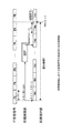
このL1帯、C/Aコードと呼ばれる送信信号は、送信信号速度、すなわち、チップレートが1.023MHzであり、例えばいわゆるGold符号等の符号長が1023の擬似ランダムノイズ(Pseudo-random Noise;PN)系列の拡散符号で、50bpsのデータを直接拡散した信号により、周波数が1575.42MHzの搬送波(以下、キャリアという。)に対して2相位相変調方式(Binary Phase Shift Keying;以下、BPSK変調方式という。)に基づく変調を施した信号である。この場合、符号長が1023であることから、C/Aコードは、図14中1段目に示すように、拡散符号が1023チップを1周期として、すなわち、1周期=1ミリ秒(msec)として、繰り返すものとなる。
【0006】
このC/Aコードの拡散符号は、GPS衛星毎に異なっているが、どのGPS衛星が、どの拡散符号を用いるかは、予めGPS受信機によって検知できるようになされている。また、GPS受信機は、後述する航法メッセージにより、どのGPS衛星からの信号をその地点及びその時点で受信することができるかが把握できるようになされている。そのため、GPS受信機は、例えば3次元測位であれば、その地点及びその時点で取得することができる少なくとも4個以上のGPS衛星からの電波を受信してスペクトラム逆拡散を施し、測位演算を行うことにより、自己の位置を算出する。
【0007】
また、GPS衛星からの信号データの1ビットは、同図中2段目に示すように、拡散符号の20周期分、すなわち、20ミリ秒単位として伝送される。すなわち、データの伝送速度は、上述したように、50bpsである。さらに、拡散符号の1周期分の1023チップは、ビットが"1"であるときと"0"であるときとでは、反転したものとなる。
【0008】
さらに、GPS衛星からの信号は、同図中3段目に示すように、30ビット、すなわち、600ミリ秒で1ワードを形成する。さらにまた、GPS衛星からの信号は、同図中4段目に示すように、10ワード、すなわち、6秒で1サブフレームを形成する。そして、GPS衛星からの信号には、同図中5段目に示すように、1サブフレームの先頭のワードに、データが更新されたときであっても常に規定のビットパターンとされるプリアンブルが挿入され、このプリアンブルに後続してデータが伝送されてくる。
【0009】
さらにまた、GPS衛星からの信号は、5サブフレーム、すなわち、30秒で1フレームを形成する。そして、GPS衛星からの信号においては、上述した航法メッセージが、この1フレームのデータ単位で伝送されてくる。
【0010】
この1フレームのデータのうちの始めの3個のサブフレームは、エフェメリス(Ephemeris)情報と呼ばれるGPS衛星固有の情報である。このエフェメリス情報には、GPS衛星の軌道を求めるためのパラメータと、GPS衛星からの信号の送出時刻とが含まれる。
【0011】
全てのGPS衛星は、原子時計を備えることによって共通の時刻情報を用いており、エフェメリス情報に含まれるGPS衛星からの信号の送出時刻は、原子時計の1秒単位とされている。また、GPS衛星の拡散符号は、原子時計に同期したものとして生成される。
【0012】
エフェメリス情報に含まれる軌道情報は、数時間毎に更新されるが、その更新が行われるまでは同一の情報となる。そのため、GPS受信機は、エフェメリス情報に含まれる軌道情報をメモリに保持しておくことにより、数時間は同じ軌道情報を精度よく使用することができる。なお、GPS衛星からの信号の送出時刻は、TOW(Time Of Week)情報として6秒毎に更新される。
【0013】
一方、1フレームのデータのうちの残りの2個のサブフレームの航法メッセージは、アルマナック(Almanac)情報と呼ばれる全てのGPS衛星から共通に送信される情報である。このアルマナック情報は、全情報を取得するために25フレーム分必要となるものであり、各GPS衛星のおおよその位置情報や、どのGPS衛星が使用可能であるのかを示す情報等から構成される。このアルマナック情報は、数日毎に更新されるが、その更新が行われるまでは同一の情報となる。そのため、GPS受信機は、アルマナック情報をメモリに保持しておくことにより、数日は同じ情報を精度よく使用することができる。しかし、GPS受信機は、精度は多少落ちるものの、数か月の間、同じアルマナック情報を使用することもできる。
【0014】
GPS受信機は、GPS衛星からの信号を受信して上述したデータを得るために、まず、キャリアを除去した後、受信しようとするGPS衛星で用いられているC/Aコードと同じ拡散符号を用いて、そのGPS衛星からの信号について、C/Aコードの位相同期をとることによってGPS衛星からの信号を捕捉し、スペクトラム逆拡散を行う。GPS受信機は、C/Aコードとの位相同期をとってスペクトラム逆拡散を行うと、ビットが検出され、GPS衛星からの信号に基づいて時刻情報等を含む航法メッセージを取得することが可能となる。
【0015】
GPS受信機は、GPS衛星からの信号の捕捉をC/Aコードの位相同期探索によって行うが、この位相同期探索として、自己が発生する拡散符号とGPS衛星からの受信信号の拡散符号との相関を検出し、例えば、その相関検出結果の相関値が予め定められた値よりも大きい場合に、両者が同期しているものと判定する。そして、GPS受信機は、同期がとれていないものと判定した場合には、何らかの同期手法を用いて、自己が発生する拡散符号の位相を制御し、受信信号の拡散符号と同期させるようにしている。
【0016】
ところで、GPS衛星からの信号は、上述したように、データを拡散符号で拡散した信号によってキャリアをBPSK変調方式に基づいて変調した信号である。したがって、GPS受信機は、GPS衛星からの信号を受信するには、拡散符号のみならず、キャリア及びデータの同期をとる必要があるが、拡散符号とキャリアの同期を独立に行うことはできない。
【0017】
また、GPS受信機は、通常、受信信号のキャリア周波数を数MHz以内の中間周波数(Intermediate Frequency;以下、IFという。)に変換することによって受信信号をIF信号に変換し、このIF信号で上述した同期検出処理を行う。このIF信号におけるキャリア(以下、IFキャリアという。)には、主に、GPS衛星の移動速度に応じたドップラシフトによる周波数誤差分と、受信信号をIF信号に変換する際にGPS受信機の内部で生成する局部発振器の周波数誤差分とが含まれる。
【0018】
したがって、GPS受信機においては、これらの周波数誤差要因によってIFキャリア周波数が未知であることから、その周波数のサーチが必要となる。また、拡散符号の1周期内での同期点(同期位相)は、GPS受信機とGPS衛星との位置関係に依存することに起因して未知であることから、GPS受信機においては、上述したように、何らかの同期手法が必要となる。
【0019】
従来のGPS受信機では、キャリアについての周波数サーチと、スライディング相関器による同期捕捉、DLL(Delay Locked Loop)及びコスタスループによる同期保持とを組み合わせた同期手法を用いている。以下、この同期手法について説明する。
【0020】
GPS受信機の拡散符号の発生器を駆動するクロックは、当該GPS受信機に用意されている基準周波数発振器を分周したものが一般に用いられる。この基準周波数発振器としては、高精度の水晶発振器が用いられ、GPS受信機は、この基準周波数発振器の出力に基づいて、GPS衛星からの受信信号をIF信号に変換するために用いる局部発振信号を生成する。
【0021】
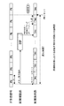
ここで、周波数サーチについての処理内容を図15に示す。GPS受信機は、拡散符号の発生器を駆動するクロック信号の周波数が、ある周波数f1であるときの拡散符号についての位相同期探索を行う。すなわち、GPS受信機は、拡散符号の位相を1チップずつ順次ずらしていくことによって各チップ位相のときのGPS衛星からの受信信号と拡散符号との相関を検出し、相関のピークを検出することにより、同期がとれる位相を検出する。また、GPS受信機は、クロック信号の周波数がf1であるときにおいて、1023チップ分の位相探索の全てで同期する位相が存在しない場合には、例えば基準周波数発振器に対する分周比を変化させ、クロック信号の周波数を他の周波数f2に変更し、同様に1023チップ分の位相探索を行う。GPS受信機は、このような動作を、クロック信号の周波数をステップ的に変化させて繰り返すことによって周波数サーチを実現する。
【0022】
そして、GPS受信機は、このような周波数サーチを行うことによって同期可能とされるクロック信号の周波数を検出すると、そのクロック信号の周波数で最終的な拡散符号の位相同期を行う。これにより、GPS受信機は、水晶発振器の発振周波数にずれがある場合であっても、GPS衛星からの信号を捕捉することが可能となる。
【0023】
しかしながら、このような従来の同期手法は、原理的には高速同期には不向きである。GPS受信機においては、拡散符号及びIFキャリアの同期に時間を要すると反応が遅くなり、使用上において不便を生じる。そのため、実際のGPS受信機においては、この欠点を補うため、多チャンネル化して並列処理によって同期捕捉までの時間を短縮している。
【0024】
一方、上述したスライディング相関を用いた手法に代わってスペクトラム拡散信号の同期捕捉を高速に行う手法としては、マッチドフィルタの利用がある。マッチドフィルタは、いわゆるトランスバーサルフィルタによってディジタル的に実現可能である。また、マッチドフィルタとしては、近年のDSP(Digital Signal Processor)に代表されるハードウェアの能力の向上により、高速フーリエ変換(Fast Fourier Transform;以下、FFTという。)を利用したディジタルマッチドフィルタによって拡散符号の同期を高速に行う手法が実現されている。後者は、古くから知られる相関計算の高速化手法に基づくものである。
【0025】
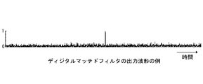
GPS受信機は、これらのマッチドフィルタを用いることにより、相関がある場合には、例えば図16に出力波形の1周期分を示すように、相関のピークを検出する。このピークの位置は、拡散符号の先頭を示すものである。GPS受信機は、このピークを検出することにより、同期を捕捉、すなわち、受信信号における拡散符号の位相を検出することができる。また、GPS受信機は、例えば上述したFFTを利用したディジタルマッチドフィルタを用い、FFTの周波数領域での操作を行うことにより、拡散符号の位相とともにIFキャリア周波数を検出することができる。そして、GPS受信機は、拡散符号の位相を擬似距離に換算し、少なくとも4個のGPS衛星が検出された場合には当該GPS受信機の位置を算出することができ、また、IFキャリア周波数に基づいて当該GPS受信機の速度を算出することができる。
【0026】
【発明が解決しようとする課題】
ところで、上述したC/Aコードを利用したGPS受信機においては、上述した発振器によって生成する発振信号の周波数である源発振周波数として、C/Aコードのチップレートである1.023MHzの倍数が用いられることが多い。例えば、GPS受信機においては、チップレートの16倍である16.368MHzを源発振周波数とした場合には、ベースバンド信号を処理するディジタル信号処理部の動作クロックを源発振器と同じ周波数である16.368MHzとし、GPS衛星からの受信信号をIF信号に変換するために用いる局部発振信号の周波数を16.368MHz×96=1571.328MHzとし、IF信号の周波数を4.092MHzとするのが典型的である。この場合、GPS受信機においては、源発振周波数を変更すると、IF信号の周波数が大きく変化することになる。
【0027】
例えば、GPS受信機においては、源発振周波数を単純に16.368MHzから16MHzに変更した場合には、IF信号の周波数は39.42MHzへと大幅に変更され、ベースバンド処理では対応しがたいものとなる。また、GPS受信機においては、他の例として、源発振周波数を16.4MHzに変更した場合には、IF信号の周波数は1.02MHzとなり、ベースバンド処理で十分対応できるものとなるが、ダウンコンバートするための帯域通過フィルタ(Band Pass Filter;以下、BPFという。)が4.092MHzを中心とする帯域固定である場合には、IF信号を大幅に減衰させてしまうことになる。
【0028】
また、GPS受信機においては、スペクトル拡散信号を復調するための上述したDLL及びコスタスループ、並びにIF信号を蓄積して所定のサンプリング周波数でサンプリングするためのサンプリングクロックに用いる源発振周波数に基づくNCO(Numeric Controlled Oscillator)の周波数範囲も変化することになる。
【0029】
このように、GPS受信機においては、源発振周波数を変更すると、ベースバンド処理に適応した対応ができなかった。
【0030】
ここで、GPS受信機の利用例としては、携帯電話機等の携帯端末をはじめとする所定の機能を有する電子機器に当該GPS受信機の機能を組み込むものがあげられる。この場合、電子機器には、クロック用にそれぞれ異なる独自の周波数を有する信号を生成する発振器が搭載されることから、GPS受信機の機能を実現するための構成部分であるGPSユニット用に新たに発振器を搭載することは、コストアップ及び電子機器の大型化につながる他、EMC(Electro Magnetic
Compatibility)の観点からは新たな不要輻射源にもなる。
【0031】
したがって、電子機器においては、GPSユニット用のクロックも当該電子機器に搭載されている発振器から得られるようにするのが好ましい。しかしながら、発振器の周波数は、電子機器によって異なることから、GPSユニットにおいては、どの発振周波数でも対応できるように、受信信号をIF信号にダウンコンバートする周波数変換部及びその他のディジタル信号処理部が設計されている必要がある。
【0032】
これらの問題は、GPS受信機の機能に限ったものではなく、GPS受信機の機能以外の所定の機能を実現する各種ユニットを所定の電子機器に組み込む場合に共通のものである。
【0033】
本発明は、このような実情に鑑みてなされたものであり、様々な発振周波数に対応することができ、また、所定の機能を有する電子機器に既に搭載されている発振器からの発振周波数を源発振周波数として利用することによってコストダウン及び小型化を図ることができる復調装置を提供することを目的とする。また、本発明は、この復調装置を適用し、本来の所定の機能とは異なる他の機能が組み込まれた受信装置を提供することを目的とする。
【0034】
【課題を解決するための手段】
上述した目的を達成する本発明にかかる復調装置は、所定の高周波信号を復調する復調装置であって、高周波信号の周波数を所定の中間周波数に変換する周波数変換手段と、この周波数変換手段によって得られた中間周波数を有する中間周波数信号に対する所定の信号処理を施す信号処理手段と、周波数変換手段及び信号処理手段に対する設定を行う設定手段とを備え、周波数変換手段は、所定の源発振器によって生成される所定の源発振信号に基づいて、高周波信号の周波数を所定の中間周波数に変換するための局部発振周波数を有する局部発振信号を生成する局部発振信号生成手段を有し、信号処理手段は、局部発振信号生成手段と源発振器を共用し、源発振器によって生成される源発振信号に基づいて、所定の周波数を有する信号を生成する信号生成手段を有し、局部発振信号生成手段は、源発振信号の源発振周波数に拘泥せずに中間周波数が所定の範囲内の値となるように、源発振器によって生成される源発振信号の任意の源発振周波数に応じて、設定手段を介して分周比が可変的に設定されることによって局部発振信号の局部発振周波数を可変とし、信号生成手段は、源発振器によって生成される源発振信号の任意の源発振周波数に応じて、設定手段を介して分周比が可変的に設定されることによって信号の周波数を可変とすることを特徴としている。
【0035】
このような本発明にかかる復調装置は、少なくとも局部発振信号生成手段と信号生成手段との源発振器を共用し、源発振信号の源発振周波数に拘泥せずに中間周波数が所定の範囲内の値となるように、任意の源発振周波数に応じて、少なくとも局部発振信号生成手段と信号生成手段との分周比が設定手段を介して可変的に設定される。
【0036】
また、上述した目的を達成する本発明にかかる受信装置は、衛星からの信号を受信して自己の位置及び速度を算出する測位ユニットが組み込まれた受信装置であって、衛星からの信号を受信する受信手段と、この受信手段によって受信した所定の高周波信号の周波数を所定の中間周波数に変換する周波数変換手段と、この周波数変換手段によって得られた中間周波数を有する中間周波数信号に対する所定の信号処理を施す信号処理手段と、周波数変換手段及び信号処理手段に対する設定を行う設定手段と、測位ユニットとは異なる所定の機能を実現する他のユニットの動作クロックを生成するために設けられ、所定の源発振信号を有する源発振信号を生成する源発振器とを備え、周波数変換手段は、源発振器によって生成される源発振信号に基づいて、高周波信号の周波数を中間周波数に変換するための局部発振周波数を有する局部発振信号を生成する局部発振信号生成手段を有し、信号処理手段は、局部発振信号生成手段と源発振器を共用し、源発振器によって生成される源発振信号に基づいて、所定の周波数を有する信号を生成する信号生成手段を有し、局部発振信号生成手段は、源発振信号の源発振周波数に拘泥せずに中間周波数が所定の範囲内の値となるように、源発振器によって生成される源発振信号の任意の源発振周波数に応じて、設定手段を介して分周比が可変的に設定されることによって局部発振信号の局部発振周波数を可変とし、信号生成手段は、源発振器によって生成される源発振信号の任意の源発振周波数に応じて、設定手段を介して分周比が可変的に設定されることによって信号の周波数を可変とすることを特徴としている。
【0037】
このような本発明にかかる受信装置は、測位ユニットにおける少なくとも局部発振信号生成手段と信号生成手段との源発振器を共用するとともに、この源発振器として、測位ユニットとは異なる所定の機能を実現する他のユニットの動作クロックを生成するために設けられた源発振器を共用し、源発振信号の源発振周波数に拘泥せずに中間周波数が所定の範囲内の値となるように、任意の源発振周波数に応じて、少なくとも局部発振信号生成手段と信号生成手段との分周比が設定手段を介して可変的に設定される。
【0038】
【発明の実施の形態】
以下、本発明を適用した具体的な実施の形態について図面を参照しながら詳細に説明する。
【0039】
この実施の形態は、人工衛星を利用して地上における移動体の位置を測定するいわゆるGNSS(Global Navigation Satellites System)システムの一種である全地球測位システム(Global Positioning System;以下、GPSという。)を適用したものであり、少なくとも4個以上のGPS衛星からの信号を受信して、その受信信号に基づいて自己の位置を算出するGPS受信機の機能が組み込まれた携帯電話機である。この携帯電話機は、GPS受信機の機能を実現するための構成部分であるGPSユニットによってL1帯、C/A(Clear and Acquisition)コードと呼ばれるスペクトラム拡散信号電波を受信信号として受信するものであって、GPSユニット用のクロックを生成するための発振器を通常の電話機能に必要となるクロックを生成するための発振器と共用し、この発振器の任意の発振周波数に応じて、GPSユニットにおける各部の設定を可変とすることにより、様々な発振周波数に対応することを可能とするとともに、コストダウン及び小型化を図ることができるものである。
【0040】
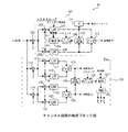
なお、この携帯電話機におけるGPSユニットは、図1に示すように、受信した受信信号を復調する際に、自己が発生する擬似ランダムノイズ(Pseudo-random Noise;PN)系列の拡散符号と受信信号における拡散符号との同期を捕捉する機能と、拡散符号と搬送波(以下、キャリアという。)との同期を保持する機能とを分離することにより、小さい回路規模のもとに、同期捕捉を高速化することができるものである。
【0041】
携帯電話機10は、同図に示すように、通常の電話機能を実現するユニットである電話ユニット11と、所定の発振周波数を有する発振信号D1を生成する水晶発振器(X'tal Oscillator;以下、XOという。)12と、このXO12とは異なる所定の発振周波数FOSCを有する発振信号D2を生成する温度補償型水晶発振器(Temperature Compensated X'tal Oscillator;以下、TCXOという。)13と、このTCXO13から供給される発振信号D2を逓倍(multiply)及び/又は分周(divide)する逓倍/分周器14とを備える。
【0042】
電話ユニット11は、例えば、受信した信号に対するベースバンド処理や音声変換処理といった通常の電話機能を実現する各部を総称したユニットである。この電話ユニット11は、TCXO13から供給される発振信号D2の発振周波数FOSCに基づくクロックを動作クロックとして用いて動作する。
【0043】
XO12は、例えば32.768kHz程度の所定の発振周波数を有する発振信号D1を生成する。XO12は、生成した発振信号D1を後述するRTC(Real Time Clock)28に供給する。
【0044】
TCXO13は、本来、電話ユニット11の動作クロックに用いるために設けられるものであって、XO12とは異なる例えば16.384MHz程度の所定の発振周波数FOSCを有する発振信号D2を生成する。TCXO13は、生成した発振信号D2を電話ユニット11、逓倍/分周器14、及び後述する周波数シンセサイザ19等に供給する。
【0045】
逓倍/分周器14は、後述するCPU(Central Processing Unit)27から供給される制御信号D3に基づいて、TCXO13から供給される発振信号D2を、所定の逓倍率で逓倍し、及び/又は所定の分周比で分周する。逓倍/分周器14は、逓倍及び/又は分周した発振信号D4を後述する同期捕捉部25、後述する同期保持部26、CPU27、後述するタイマ29、及び後述するメモリ30に供給する。
【0046】
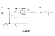
また、携帯電話機10は、GPS衛星から送信されてきたRF(Radio Frequency)信号を受信するアンテナ15と、このアンテナ15によって受信された受信RF信号D5を増幅するローノイズ・アンプ(Low Noise Amplifier;以下、LNAという。)16と、このLNA16によって増幅された増幅RF信号D6のうち所定の周波数帯域成分を通過させる帯域通過フィルタ(Band Pass Filter;以下、BPFという。)17と、このBPF17によって通過された増幅RF信号D7をさらに増幅する増幅器18と、TCXO13から供給される発振信号D2に基づいて所定の周波数FLOを有する局部発振信号D10を生成する周波数シンセサイザ19と、増幅器18によって増幅された所定の周波数FRFを有する増幅RF信号D8に対して周波数シンセサイザ19から供給された局部発振信号D10を乗算するミキサ20と、このミキサ20によって乗算されることによってダウンコンバートされた所定の周波数FIFを有する中間周波数(Intermediate Frequency;以下、IFという。)信号D11を増幅する増幅器21と、この増幅器21によって増幅された増幅IF信号D12のうち所定の周波数帯域成分を通過させる低域通過フィルタ(Low Pass Filter;以下、LPFという。)22と、このLPF22によって通過されたアナログ形式の増幅IF信号D13をディジタル形式の増幅IF信号D14に変換するアナログ/ディジタル変換器(Analog/Digital Converter;以下、A/Dという。)23とを備える。
【0047】
アンテナ15は、GPS衛星から送信されてきた周波数が1575.42MHzのキャリアが拡散されたRF信号を受信する。このアンテナ15によって受信された受信RF信号D5は、LNA16に供給される。
【0048】
LNA16は、アンテナ15によって受信された受信RF信号D5を増幅する。LNA16は、増幅した増幅RF信号D6をBPF17に供給する。
【0049】
BPF17は、いわゆるSAW(Surface Acoustic Wave)フィルタからなり、LNA16によって増幅された増幅RF信号D6のうち所定の周波数帯域成分を通過させる。このBPF17によって通過された増幅RF信号D7は、増幅器18に供給される。
【0050】
増幅器18は、BPF17によって通過された増幅RF信号D7をさらに増幅する。増幅器18は、増幅した所定の周波数FRF、すなわち、1575.42MHzの増幅RF信号D8をミキサ20に供給する。
【0051】
周波数シンセサイザ19は、CPU27から供給される制御信号D9による制御のもとに、TCXO13から供給される発振信号D2に基づいて所定の周波数FLOを有する局部発振信号D10を生成する。このとき、周波数シンセサイザ19は、詳細は後述するが、TCXO13によって生成される発振信号D2の発振周波数FOSCに応じて設定を可変とする。周波数シンセサイザ19は、生成した局部発振信号D10をミキサ20に供給する。
【0052】
ミキサ20は、増幅器18によって増幅された所定の周波数FRFを有する増幅RF信号D8に対して周波数シンセサイザ19から供給された局部発振信号D10を乗算することによって増幅RF信号D8をダウンコンバートし、例えば1.023MHz程度の所定の周波数FIFを有するIF信号D11を生成する。このミキサ20によって生成されたIF信号D11は、増幅器21に供給される。
【0053】
増幅器21は、ミキサ20によってダウンコンバートされたIF信号D11を増幅する。増幅器21は、増幅した増幅IF信号D12をLPF22に供給する。
【0054】
LPF22は、増幅器21によって増幅された増幅IF信号D12のうち所定の周波数よりも低域成分を通過させる。なお、LPF22は、詳細は後述するが、必要に応じて、TCXO13によって生成される発振信号D2の発振周波数FOSCに応じて通過周波数帯域等の特性を可変とする。このLPF22によって通過された増幅IF信号D13は、A/D23に供給される。
【0055】
A/D23は、LPF22によって通過されたアナログ形式の増幅IF信号D13をディジタル形式の増幅IF信号D14に変換する。このA/D23によって変換された増幅IF信号D14は、同期捕捉部25及び同期保持部26に供給される。
【0056】
なお、携帯電話機10においては、これらの各部のうち、LNA16、BPF17、増幅器18,21、周波数シンセサイザ19、ミキサ20、LPF22、及びA/D23は、アンテナ15によって受信された1575.42MHzの高い周波数を有する受信RF信号D5を、ディジタル信号処理が施しやすいように、例えば1.023MHz程度の低い周波数FIFを有する増幅IF信号D14にダウンコンバートする周波数変換部24として構成される。
【0057】
さらに、携帯電話機10は、自己が発生する拡散符号とA/D23から供給される増幅IF信号D14における拡散符号との同期捕捉及び増幅IF信号D14におけるキャリア周波数の検出を行う同期捕捉部25と、A/D23から供給される増幅IF信号D14における拡散符号とキャリアとの同期保持及びメッセージの復調を行う同期保持部26と、各部を統括的に制御して各種演算処理を行うCPU27と、XO12から供給される発振信号D1に基づいて時間を計測するRTC28と、CPU27の内部時計としてのタイマ29と、RAM(Random Access Memory)やROM(Read Only Memory)等からなるメモリ30とを備える。
【0058】
同期捕捉部25は、CPU27の制御のもとに、逓倍/分周器14から供給される逓倍及び/又は分周された発振信号D4に基づいて、A/D23から供給される増幅IF信号D14における拡散符号の同期捕捉を粗い精度で行うとともに、増幅IF信号D14におけるキャリア周波数の検出を行う。このとき、同期捕捉部25は、詳細は後述するが、TCXO13によって生成される発振信号D2の発振周波数FOSCに応じて設定を可変とする。同期捕捉部25は、検出したGPS衛星を識別するための衛星番号、拡散符号の位相、及びキャリア周波数を同期保持部26及びCPU27に供給する。
【0059】
同期保持部26は、CPU27の制御のもとに、逓倍/分周器14から供給される逓倍及び/又は分周された発振信号D4に基づいて、A/D23から供給される増幅IF信号D14における拡散符号とキャリアとの同期保持を行うとともに、増幅IF信号D14に含まれる航法メッセージの復調を行う。このとき、同期保持部26は、詳細は後述するが、TCXO13によって生成される発振信号D2の発振周波数FOSCに応じて設定を可変とする。また、同期保持部26は、同期捕捉部25から供給される衛星番号、拡散符号の位相、及びキャリア周波数を初期値として動作を開始する。同期保持部26は、複数のGPS衛星からの増幅IF信号D14についての同期保持を並列的に行い、検出した拡散符号の位相、キャリア周波数、及び航法メッセージをCPU27に供給する。
【0060】
CPU27は、同期保持部26から供給される拡散符号の位相、キャリア周波数、及び航法メッセージを取得し、これらの各種情報に基づいて、当該携帯電話機10の位置及び速度を算出するとともに、航法メッセージから得られるGPS衛星の正確な時間情報に基づいて、当該携帯電話機10の時間情報を補正するといったGPSに関する各種演算処理を行う。また、CPU27は、当該携帯電話機10の各部及び各種ペリフェラル、並びに外部との入出力(Input/Output)に関する制御を統括的に行う。
【0061】
RTC28は、XO12から供給される発振信号D1に基づいて、時間を計測する。このRTC28によって計測される時間情報は、GPS衛星の正確な時間情報が得られるまでの間に代用されるものであって、GPS衛星の正確な時間情報を得たCPU27がXO12を制御することによって適宜補正される。
【0062】
タイマ29は、CPU27の内部時計として機能するものであり、各部の動作に必要となる各種タイミング信号の生成及び時間参照に用いられる。例えば、携帯電話機10においては、同期捕捉部25が同期捕捉した拡散符号の位相に合わせて同期保持部26が後述する拡散符号発生器の動作を開始させるタイミングを、このタイマ29によって参照する。
【0063】
メモリ30は、RAMやROM等からなる。メモリ30においては、CPU27等による各種処理を行う際のワークエリアとしてRAMが用いられるとともに、入力した各種データをバッファリングする際や、演算過程で生成される中間データ及び演算結果データを保持する際にもRAMが用いられる。また、メモリ30においては、各種プログラムや固定データ等を記憶する手段としてROMが用いられる。
【0064】
なお、携帯電話機10においては、これらの同期捕捉部25、同期保持部26、CPU27、RTC28、タイマ29、メモリ30は、ベースバンド処理部として構成される。
【0065】
このような各部を備える携帯電話機10においては、少なくとも、XO12、TCXO13、アンテナ15、LNA16、及びBPF17を除く各部を、集積回路化した1チップからなる復調回路31として構成することができる。
【0066】
携帯電話機10は、通常の電話機能を実現するのは勿論のこと、GPSユニットを用いたGPS受信機として機能する場合には、少なくとも4個以上のGPS衛星からのRF信号を受信して、このRF信号を周波数変換部24によってIF信号に変換した後、同期捕捉部25によって拡散符号の同期捕捉及びキャリア周波数の検出を行い、同期保持部26によって拡散符号とキャリアとの同期保持及び航法メッセージの復調を行う。そして、携帯電話機10は、拡散符号の位相、キャリア周波数、及び航法メッセージに基づいて、CPU27によって当該携帯電話機10の位置及び速度を算出する。
【0067】
つぎに、携帯電話機10における同期捕捉部25及び同期保持部26について説明する。なお、携帯電話機10は、上述したように、同期捕捉の機能と同期保持の機能とを、同期捕捉部25及び同期保持部26に分離したものである。ここでは、このように機能を分離した理由についても併せて説明する。
【0068】
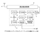
同期捕捉部25は、上述したように、IF信号における拡散符号の同期捕捉及びキャリア周波数の検出を高速に行う。同期捕捉部25は、拡散符号の同期捕捉を高速に行うためにマッチドフィルタを利用する。具体的には、同期捕捉部25は、マッチドフィルタとして、例えば図2に示すように、高速フーリエ変換(Fast Fourier Transform;以下、FFTという。)を利用したディジタルマッチドフィルタ50を用いることができる。
【0069】
具体的には、ディジタルマッチドフィルタ50は、同図に示すように、上述したアンテナ15及び周波数変換部24によって得られる増幅IF信号D14に対応するIF信号を、TCXO13によって生成される発振信号D2に基づく所定のサンプリング周波数で入力信号をサンプリングするサンプラ51によってサンプリングした上で入力する。ディジタルマッチドフィルタ50は、サンプラ51によってサンプリングされたIF信号をバッファリングするメモリ52と、このメモリ52によってバッファリングされたIF信号を読み出してFFT処理を施すFFT処理部53と、このFFT処理部53によってFFT処理が施されて得られた周波数領域信号をバッファリングするメモリ54と、GPS衛星からのRF信号における拡散符号と同じ拡散符号を発生する拡散符号発生器55と、この拡散符号発生器55によって発生された拡散符号に対してFFT処理を施すFFT処理部56と、このFFT処理部56によってFFT処理が施されて得られた周波数領域信号をバッファリングするメモリ57と、メモリ54にバッファリングされている周波数領域信号とメモリ57にバッファリングされている周波数領域信号とのうちいずれか一方の複素共役と他方とを乗算する乗算器58と、この乗算器58によって乗算された周波数領域信号に対して逆FFT(Inversed Fast Fourier Transform;以下、IFFTという。)処理を施すIFFT処理部59と、このIFFT処理部59によってIFFT処理が施されて得られた相関関数に基づいてGPS衛星からのRF信号における拡散符号と拡散符号発生器55によって発生された拡散符号との相関のピークを検出するピーク検出器60とを有する。
【0070】
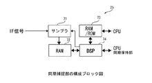
このようなディジタルマッチドフィルタ50は、実際には、FFT処理部53,56、拡散符号発生器55、乗算器58、IFFT処理部59、及びピーク検出器60の各部をDSP(Digital Signal Processor)によって実行されるソフトウェアとして実装される。すなわち、ディジタルマッチドフィルタ50を適用した同期捕捉部25は、例えば図3に示すように、上述したサンプラ51に相当するサンプラ71と、上述したメモリ52に相当するRAM72と、上述したメモリ54,57とDSPのプログラムエリア及びワークエリアとを含むRAM/ROM73と、上述したFFT処理部53,56、拡散符号発生器55、乗算器58、IFFT処理部59、及びピーク検出器60の処理を実行するDSP74とから構成される。
【0071】
同期捕捉部25は、例えば、1.023MHzのIF信号をサンプラ71によって4.096MHzでサンプリングし、DSP74によってディジタルマッチドフィルタ50と等価な演算を行うことにより、拡散符号の同期捕捉、すなわち、IF信号における拡散符号の位相検出を1/4チップの精度で行うことができる。また、この同期捕捉部25は、RAM72の容量が16ミリ秒分であるものとすると、DSP74によってFFTの周波数領域での操作を行うことにより、1/16kHz(±1/32kHz)の精度で、IF信号におけるキャリア(以下、IFキャリアという。)周波数を検出することができる。同期捕捉部25は、RAM72に記憶したIF信号には複数のGPS衛星からの信号が含まれていることから、各GPS衛星の拡散符号との相関を算出することにより、複数のGPS衛星を検出することができる。
【0072】
携帯電話機10は、この同期捕捉部25によって検出した少なくとも4個以上のGPS衛星に対する拡散符号の位相とキャリア周波数とに基づいて、当該携帯電話機10の位置と速度とを算出することができる。
【0073】
ただし、携帯電話機10においては、拡散符号の位相検出精度としての上述した1/4チップ、及びキャリア周波数の検出精度としての1/16kHzのもとに得られる当該携帯電話機10の位置及び速度の算出結果は十分な精度とは言い難いものである。携帯電話機10においては、精度を向上させるためには、サンプラ71によるサンプリング周波数を高くする、IF信号を記憶する時間長を長くする、といった処理が必要となるが、これにともない、RAM72等のメモリの容量が増大し、且つ、拡散符号の位相及びキャリア周波数を検出するまでの処理時間が長くなる事態が想定される。また、携帯電話機10においては、同期捕捉部25が外部から航法メッセージを受け取らないものとすると、少なくとも4個以上のGPS衛星からの航法メッセージを20ミリ秒毎に復調する必要があることから、DSP74は、常に、同期の検出と航法メッセージの復調とを極めて高速に行う必要がある。これらの問題は、ハードウェアのサイズの膨大化によるコストアップと消費電力の増大化を招来する。
【0074】
そこで、携帯電話機10においては、粗い精度での同期捕捉を同期捕捉部25によって行い、複数のGPS衛星の同期保持及び航法メッセージの復調を同期保持部26によって行う。
【0075】
同期捕捉部25は、検出したGPS衛星の衛星番号、その拡散符号の位相、及びキャリア周波数を同期保持部26に供給する。一方、同期保持部26は、同期捕捉部25から供給されるこれらの各種情報を初期値として動作を開始する。同期保持部26は、拡散符号の位相に基づいて、後述するDLL(Delay Locked Loop)の回路で生成する拡散符号の開始タイミングを合わせる。なお、携帯電話機10は、生成する拡散符号として、検出したGPS衛星の衛星番号に対応するものを設定する。このとき、携帯電話機10においては、ドップラシフト、及びTCXO13等の発振器によって生成される発振信号の発振周波数の誤差の影響を受けるが、基本的に拡散符号は1ミリ秒の周期で繰り返されるものであることから、DLLの回路で生成する拡散符号の開始タイミングは、1ミリ秒の整数倍ずらしても構わない。
【0076】
なお、IFキャリア周波数は、IF信号を上述したRAM72等のメモリに取り込むためのサンプリングクロックを生成しているTCXO13の誤差を含むことから、上述した分解能の問題を除去したとしても、正確な値、すなわち、キャリア周波数とドップラシフト量との和ではない。しかしながら、携帯電話機10においては、同期捕捉部25と同期保持部26とが同じ発振器、すなわち、TCXO13を発振源とするクロックで動作している場合には、両者で全く同じ周波数誤差を有することから、同期保持部26が同期捕捉部25によって検出されたIFキャリア周波数を初期値として動作を開始することには何らの問題がない。
【0077】
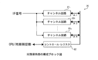
同期保持部26は、複数のGPS衛星の同期保持を並列的に行うことから、例えば図4に示すように、複数個の独立したチャンネル回路811,812,・・・,81Nを有する。チャンネル回路811,812,・・・,81Nは、それぞれ、コントロール・レジスタ82の設定によって同期捕捉部25による個々の検出結果に対して割り当てられる。
【0078】
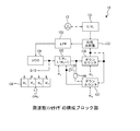
チャンネル回路811,812,・・・,81Nは、それぞれ、図5に示すように、従来のGPS受信機における同期捕捉及び同期保持の双方を実現するIFキャリア同期用のコスタスループ101と拡散符号同期用のDLL102とを組み合わせた回路と基本的には同様に構成される。
【0079】
すなわち、チャンネル回路811,812,・・・,81Nにおいては、それぞれ、同図に示すように、コスタスループ101には、上述したアンテナ15及び周波数変換部24によって得られる増幅IF信号D14に対応するIF信号に対して、後述する拡散符号発生器(PN Generator;以下、PNGという。)128によって発生された位相がP(Prompt)とされる拡散符号が乗算器103によって乗算された信号が入力される。一方、チャンネル回路811,812,・・・,81Nにおいては、それぞれ、DLL102には、上述したアンテナ15及び周波数変換部24によって得られる増幅IF信号D14に対応するIF信号が入力される。
【0080】
コスタスループ101においては、入力された信号に対して、NCO(Numeric Controlled Oscillator)104によって生成された再生キャリアのうちのサイン成分(同相成分)が乗算器105によって乗算される一方、NCO104によって生成された再生キャリアのうちのコサイン成分(直交成分)が乗算器106によって乗算される。コスタスループ101においては、乗算器105によって得られた同相成分の信号のうち所定の周波数帯域成分がLPF107によって通過され、この信号が位相検出器110、2値化回路111及び2乗和算出回路112に供給される。一方、コスタスループ101においては、乗算器106によって得られた直交成分の信号のうち所定の周波数帯域成分がLPF108によって通過され、この信号が位相検出器110及び2乗和算出回路112に供給される。コスタスループ101においては、LPF107,108のそれぞれから出力された信号に基づいて位相検出器110によって検出された位相情報がループフィルタ109を介してNCO104に供給される。また、コスタスループ101においては、LPF107,108のそれぞれから出力された信号が2乗和算出回路112に供給され、この2乗和算出回路112によって算出された2乗和(I2+Q2)が、位相がPとされる拡散符号についての相関値(P)として出力される。さらに、コスタスループ101においては、LPF107から出力された信号が2値化回路111に供給され、2値化されて得られた情報が航法メッセージとして出力される。
【0081】
一方、DLL102においては、入力されたIF信号に対して、PNG128によって発生された位相がPよりも進んだE(Early)とされる拡散符号が乗算器113によって乗算されるとともに、PNG128によって発生された位相がPよりも遅れたL(Late)とされる拡散符号が乗算器114によって乗算される。DLL102においては、乗算器113によって得られた信号に対して、コスタスループ101におけるNCO104によって生成された再生キャリアのうちのサイン成分が乗算器115によって乗算されるとともに、NCO104によって生成された再生キャリアのうちのコサイン成分が乗算器116によって乗算される。そして、DLL102においては、乗算器115によって得られた同相成分の信号のうち所定の周波数帯域成分がLPF117によって通過され、この信号が2乗和算出回路119に供給される。一方、DLL102においては、乗算器116によって得られた直交成分の信号のうち所定の周波数帯域成分がLPF118によって通過され、この信号が2乗和算出回路119に供給される。また、DLL102においては、乗算器114によって得られた信号に対して、コスタスループ101におけるNCO104によって生成された再生キャリアのうちのサイン成分が乗算器120によって乗算されるとともに、NCO104によって生成された再生キャリアのうちのコサイン成分が乗算器121によって乗算される。そして、DLL102においては、乗算器120によって得られた同相成分の信号のうち所定の周波数帯域成分がLPF122によって通過され、この信号が2乗和算出回路124に供給される。一方、DLL102においては、乗算器121によって得られた直交成分の信号のうち所定の周波数帯域成分がLPF123によって通過され、この信号が2乗和算出回路124に供給される。
【0082】
DLL102においては、2乗和算出回路119,124のそれぞれから出力された信号が位相検出器125に供給され、これらの信号に基づいて位相検出器125によって検出された位相情報がループフィルタ126を介してNCO127に供給され、さらに、NCO127によって生成された所定の周波数を有する信号に基づいて、PNG128によって各位相E,P,Lの拡散符号が発生される。さらに、DLL102においては、2乗和算出回路119によって算出された2乗和(I2+Q2)が、位相がEとされる拡散符号についての相関値(E)として出力される一方、2乗和算出回路124によって算出された2乗和(I2+Q2)が、位相がLとされる拡散符号についての相関値(L)として出力される。
【0083】
このように、IFキャリア同期用のコスタスループ101と拡散符号同期用のDLL102とを組み合わせた回路と同様に構成されるチャンネル回路811,812,・・・,81Nを有する同期保持部26においては、動作開始前に、GPS衛星の衛星番号、拡散符号の位相、及びキャリア周波数が初期値として設定される。この初期値の設定は、同期捕捉部25との間で直接的に通信を行うか、又は、同期捕捉部25及び当該同期保持部26を制御するCPU27を介して行うことによってなされる。
【0084】
このような同期保持部26は、以下のようにして拡散符号と同期を合わせる。すなわち、図6に示すように、同期捕捉部25がIF信号をRAM72等のメモリに取り込むタイミングでタイマを開始させ、同期捕捉部25がメモリに記憶しているIF信号に対して拡散符号の位相hを検出すると、同期保持部26は、この位相hの値を受け取った後、同じタイマによって1ミリ秒の整数倍からhだけずらした時点においてDLL102によって発生する拡散符号を開始させることにより、受信信号の拡散符号に位相を合わせる。なお、同図における"PN"は、PN系列の符号、すなわち、拡散符号を示している。
【0085】
ここで、従来のコスタスループとDLLとを組み合わせた回路においては、受信信号における拡散符号の位相が未知であることから、DLLによって発生するIFキャリア周波数と拡散符号の周期とを少しずらし、IF信号の拡散符号に対して位相をスライドしていく過程で、有意な強度の相関がある位相を検出していた。そのため、従来の回路においては、位相を検出するのに、最悪の場合、数kHzの範囲のキャリア周波数と符号長が1023の拡散符号における全ての位相とに対して検出を行うことから、同期を確立するまでにかなりの時間を要していた。
【0086】
これに対して、携帯電話機10においては、同期保持部26が従来の回路と基本的には同様の構成でありながら、同期保持部26が受け取った拡散符号の位相とIFキャリア周波数との初期値は真値から僅かにしかずれていないことから、有意な強度の相関がある位相は、誤差を含めても初期値の近辺に必ず存在する。したがって、同期保持部26は、従来の回路と同様に、まずコスタスループ101及びDLL102におけるループフィルタ109,126の制御を止めた状態にして、NCO104,127のそれぞれによって生成する信号を初期値の近辺で変化させながら有意な強度の相関を探索し、相関を検出した後には、ループフィルタ109,126のそれぞれからの制御に切り替える。これにより、同期保持部26は、DLL102による拡散符号の位相の同期確立、及びコスタスループ101によるキャリアの位相の同期確立を極めて短時間に行うことができ、以降、同期を保持し続けることができる。同期保持部26においては、IFキャリア周波数に対して、NCO104によって生成する再生キャリアの周波数を数十Hzの誤差範囲で初期値を設定できることから、LPF107,108,117,118,122,123、及びループフィルタ109,126の帯域幅を当初から狭くすることができ、S/N(Signal to Noise ratio)が高い状態で同期を確立することができる。
【0087】
携帯電話機10においては、同期保持部26を例えば1.023MHz×16=16.368MHzのクロックで動作させ、DLL102において拡散符号の位相を1/16.368MHzの時間分解能で検出すれば、1/16チップの精度で拡散符号の位相からGPS衛星までの擬似距離を算出することができ、また、コスタスループ101におけるNCO104を1Hz単位で制御できる構成にすれば、IFキャリア周波数の分解能は1Hzとなり、DLL102とコスタスループ101とによってこれらの精度で同期を保持することができる。
【0088】
以上のように、携帯電話機10においては、同期保持部26によって同期保持が行われると、DLL102によって発生する拡散符号の位相に基づいて、当該携帯電話機10の位置を連続的に算出して出力することができるとともに、コスタスループ101によって得られるIFキャリア周波数に基づいて、当該携帯電話機10の速度を連続的に算出して出力することができる。
【0089】
同期保持部26は、上述したように、同期捕捉部25から受け渡された拡散符号の位相及びIFキャリア周波数を初期値とすることにより、これらの初期値の近辺で有意な強度の相関が得られる位相を探索する。これは、携帯電話機10に搭載されているクロック源の発振器、すなわち、TCXO13が公称周波数に対して誤差を有することが1つの理由である。携帯電話機10においては、先に図2に示したFFTを利用したディジタルマッチドフィルタ50を用いて同期捕捉部25を構成した場合には、IF信号をメモリに記憶した後、DSPの処理時間分遅れて同期保持部26に検出結果が供給されることから、発振器の公称周波数FOSCとの誤差をΔFOSCとし、DSPの処理時間をT秒とすると、同期保持部26に検出結果が供給される時点では、T×ΔFOSC/FOSCの誤差が生じる。例えば、携帯電話機10においては、T=3秒とし、ΔFOSC/FOSCが±3ppmの範囲内とすると、±9マイクロ秒=約±9チップ以内の誤差が生じる。このように、携帯電話機10においては、DSPの処理時間が長くなると、その分誤差が大きくなる。
【0090】
また、携帯電話機10においては、GPS衛星と当該携帯電話機10との移動によって生じるキャリア周波数のドップラシフトも誤差を生じる要因となる。携帯電話機10においては、キャリアの周波数、すなわち、1575.42MHzをFRFとし、受信信号のドップラシフトをΔFDとすると、ドップラシフトによって拡散符号の周期、すなわち、1ミリ秒は、ほぼ(1−ΔFD/FRF)倍となり、例えば、+5〜−5kHzの範囲のドップラシフトが生じている場合には、3秒間で約−9.5〜9.5マイクロ秒=約−9.5〜9.5チップの誤差が生じる。
【0091】
これらの2つの例は、比較的現実に近い値であり、携帯電話機10においては、発振器の誤差とドップラシフトとの両者の要因を併せると、±20チップ程度の範囲内で誤差が生じることから、この範囲だけを探索して相関を検出すればよい。例えば、同期保持部26は、同期捕捉部25から供給される拡散符号の位相よりも20チップ分だけ早くDLL102によって発生する拡散符号を開始させ、そのときの拡散符号の周期として、NCO104,127の周波数設定を(1+5/1575.420)ミリ秒よりも長めに設定しておけば、IF信号に含まれるGPS衛星からの信号の拡散符号に対するスライドが+20チップだけずれた時点から開始され、適当な時間の間、拡散符号同士の位相がスライドしている状態で相関の有無を探索することができる。
【0092】
このように、従来においては、DLLとコスタスループとを用いて1023チップの範囲で、且つ、IFキャリア周波数についても発振器の誤差とドップラシフト量との範囲で変化させながら、相関検出を行っていたのに比較して、携帯電話機10においては、初期値のキャリア周波数が僅かな誤差しか有さず、相関を検出する範囲も数十分の1程度で済むことから、同期保持部26による同期確立に要する時間を極めて短時間とすることができる。
【0093】
以上のように、携帯電話機10は、同期捕捉の機能と同期保持の機能とを分離して構成することにより、同期捕捉部25によってIF信号に含まれるGPS衛星からの信号の拡散符号の位相及びIFキャリア周波数を高速に検出することができ、この検出結果に基づいて同期保持部26が速やかに同期保持動作に移行することができる。しかしながら、携帯電話機10においては、IF信号に含まれる微弱なGPS衛星の信号を検出するために処理シーケンスが増える場合、また、電力消費を抑制するために同期捕捉部25を低速のクロックで動作させている場合等には、同期捕捉部25での処理時間が長くなり、これにともない、同期保持部26による同期確立までに探索する範囲が広くなり、好ましくない。
【0094】
一般に、GPS受信機においては、周波数変換部における局部発振器とベースバンド処理部における信号処理のクロックを生成する源発振器として、共通の水晶発振器を用いるが、携帯電話機10においては、これと同様に、先に図1に示したように、周波数変換部24における局部発振器の源発振器と同期捕捉部25及び同期保持部26の動作クロックの源発振器とを、TCXO13に共通化する。そして、同期保持部26は、同期捕捉部25によって検出したIFキャリア周波数とTCXO13の公称値に基づく例えば1.023MHzの中間周波数FIFとの差分をΔFIFとし、1575.42MHzであるGPS衛星からの信号のキャリア周波数をFRFとし、同期捕捉部25がIF信号をメモリに取り込んでから同期捕捉処理に要した時間をT秒とし、拡散符号の位相をhとすると、図7に示すように、拡散符号の位相hをh+Δh(Δh=−T×ΔFIF/FRF)のように補正する。例えば、ΔFIF=+3kHz、T=10秒の場合には、Δh=−19マイクロ秒=約−19チップとなる。同期保持部26は、このような補正を行うことにより、TCXO13の発振周波数FOSCの誤差とドップラシフトとによって生じる拡散符号の位相のずれを極めて正確に補正することができ、同期捕捉部25による同期捕捉処理に時間を数十秒要した場合であっても、ほぼ1チップ程度の範囲での探索で同期を確立することができる。
【0095】
このような補正が可能な理由は、以下のとおりである。
【0096】
携帯電話機10においては、周波数変換部24によってGPS衛星からの信号の既知であるキャリア周波数FRFを既知である中間周波数FIFに変換するために、公称発振周波数FOSCのTCXO13に基づいて周波数シンセサイザ19によって局部発振周波数FLO=N×FOSC(Nは定数数、N>>1)を生成し、FIF=FRF−FLOとなるようにする。ここで、実際に受信するGPS衛星からの信号には、中間周波数FIFに対してTCXO13の発振周波数FOSCの誤差とドップラシフトとによって生じる誤差ΔFIFが加わったものである。すなわち、携帯電話機10においては、ドップラシフト量をΔFDとし、TCXO13による公称発振周波数との誤差をΔFOSCとすると、
FIF+ΔFIF=FRF+ΔFD−FLO=FRF+ΔFD−N×(FOSC+ΔFOSC)
となる。したがって、携帯電話機10においては、同期捕捉部25が検出するIFキャリア周波数は、
FIF+ΔFIF、ΔFIF=ΔFD−N×ΔFOSC
となる。ここで重要なことは、同期捕捉部25が検出することができるものはΔFIFのみであり、ΔFD,ΔFOSCは最初の同期捕捉の段階では未知であるということである。
【0097】
ここで、TCXO13によって拡散符号の1周期長である1ミリ秒を公称発振周波数でタイマがカウントした場合には、誤差ΔFOSCがあるために、実際には、1ミリ秒×FOSC/(FOSC+ΔFOSC)≒(1−ΔFOSC/FOSC)ミリ秒となる。一方、受信信号における拡散符号の1周期長さは、ドップラシフト量ΔFDにより、1ミリ秒×FRF/(FRF+ΔFD)≒(1−ΔFD/FRF)ミリ秒となる。したがって、受信信号における拡散符号の1周期長とTCXO13による公称発振周波数でカウントした1ミリ秒との比は、
(1−ΔFD/FRF)/(1−ΔFOSC/FOSC)≒1−ΔFD/FRF+ΔFOSC/FOSC
となる。さらに、この式における右辺は、変形すると、
1−ΔFIF/FRF+(ΔFOSC/FOSC)×(FIF/(N×FOSC))≒1−ΔFIF/FRF
となる。このように、携帯電話機10においては、同期捕捉部25にとって未知のパラメータであるΔFD,ΔFOSCを含まない形でかなり良好な近似をすることができる。
【0098】
この結果により、携帯電話機10においては、同期捕捉部25がIF信号をメモリに取り込んだ時点から同期捕捉処理を行い、検出した拡散符号の位相hが同期保持部26に供給されるまでの時間にT秒要した場合には、このT秒の間に同期捕捉部25が検出した拡散符号の位相から−T×ΔFIF/FRFだけずれることになる。したがって、同期保持部26は、図7に示したように、同期捕捉部25から供給された拡散符号の位相hに補正値Δh=−T×ΔFIF/FRFを加えたh+ΔhによってDLL102によって発生する拡散符号の開始タイミングを合わせることにより、同期捕捉処理時間に生じた拡散符号の位相のずれを補正することができ、これによってほぼ1チップ程度の範囲内において相関を検出することができ、極めて短時間に同期を確立することができる。携帯電話機10においては、補正値を例えばCPU27によって算出し、その算出結果を同期保持部26に供給し、同期保持部26によって位相を補正した後に、同期捕捉部25による同期捕捉処理を開始すればよい。
【0099】
このような拡散符号の位相を補正する手法において必要となる情報は、同期捕捉部25が検出したIFキャリア周波数のみであり、携帯電話機10においては、TCXO13の発振周波数FOSCの誤差もドップラシフト量も、情報として不要である。また、携帯電話機10においては、IFキャリア周波数に依存せず、FIF=FRO−FLOとなるように局部発振周波数FLOを設定する場合であっても、ΔFIFの符号を変更するのみで済む。
【0100】
さて、このような携帯電話機10は、上述したように、本来であれば電話ユニット11の動作クロックを生成するために設けられたTCXO13をGPSユニットが共用するものである。このTCXO13は、携帯電話機10の機種等によって発振周波数FOSCが多岐にわたるものである。そこで、携帯電話機10は、様々な発振周波数FOSCに対応するために、周波数変換部24及びベースバンド処理部における各部の設定を可変とする。
【0101】
具体的には、携帯電話機10は、周波数変換部24によって生成される増幅IF信号D14の周波数、すなわち、中間周波数FIFが、TCXO13によって生成する発振信号D2の発振周波数FOSCに拘泥せずに所定の範囲内の値となるように、少なくとも、周波数変換部23における周波数シンセサイザ19によって生成される局部発振信号D10の周波数である局部発振周波数FLOを可変とする。また、携帯電話機10は、ベースバンド処理部における同期保持部26として設けられるスペクトル拡散信号を復調するための上述したコスタスループ101及びDLL102のNCO104,127の周波数設定を可変とする。
【0102】
さらに、携帯電話機10においては、必要に応じて、周波数変換部24におけるLPF22の通過周波数帯域等の特性を可変とする。さらにまた、携帯電話機10は、同期捕捉部25における増幅IF信号D14を所定のサンプリング周波数でサンプリングするための上述したサンプラ71のサンプリングクロックに用いる後述するNCOの周波数範囲や、同期捕捉部25及び同期保持部26におけるコスタスループ101及びDLL102の上述したLPF107,108,117,118,122,123の通過周波数帯域等の特性、及び/又は上述したループフィルタ109,126の特性も可変とする。以下では、これらの各部について詳述する。
【0103】
まず、周波数変換部24における設定を可変とする基本的な手法について説明する。
【0104】
携帯電話機10においては、周波数FRFを有する増幅RF信号D8をダウンコンバートして周波数FIFを有するIF信号D11を生成するために、周波数シンセサイザ19における分周器の分周比を可変とすることにより、局部発振信号D10の周波数である局部発振周波数FLOを可変とする。
【0105】
具体的には、周波数シンセサイザ19は、例えば図8に示すように、CPU27によって可変的に設定される4つの設定値K1,K2,K3,K4によって分周比が可変とされるPLL(Phase Locked Loop)シンセサイザとして構成される。すなわち、この周波数シンセサイザ19は、TCXO13から供給される発振信号D2を所定の分周比で分周する分周器131と、この分周器131から供給される分周された発振信号と後述するダウンカウンタ136から供給される信号との位相を比較する位相比較器132と、この位相比較器132による比較結果信号のうち所定の周波数帯域成分を通過させるLPF133と、このLPF133によって通過された比較結果信号に基づいて所定の周波数を有する発振信号を生成する発振器である電圧制御発振器(Voltage Controlled Oscillator;以下、VCOという。)134と、このVCO134から供給される発振信号を外部からの制御によって"1"だけ異なる所定の2つの分周比で分周するパルススワロカウンタ135と、このパルススワロカウンタ135から供給される分周された信号に基づいて信号をダウンカウントするダウンカウンタ136と、後述するANDゲート140から供給される信号に基づいて信号をダウンカウントするダウンカウンタ137と、CPU27によって設定された設定値K1,K2,K3,K4を保持するレジスタやメモリ等の記憶素子138とを有する。この周波数シンセサイザ19の構成は、一般的によく用いられるものである。
【0106】
分周器131は、TCXO13から供給される発振信号D2を、CPU27によって記憶素子138に設定された設定値K1を用いて表される分周比1/K1で分周する。分周器131は、分周した発振信号を位相比較器132に供給する。この分周した発振信号は、PLLのリファレンスクロック周波数となる。
【0107】
位相比較器132は、分周器131から供給される分周された発振信号とダウンカウンタ136から供給される信号との位相を比較する。位相比較器132は、比較結果を示す比較結果信号をLPF133に供給する。
【0108】
LPF133は、PLLのループフィルタとして動作するものであり、位相比較器132から供給された比較結果信号のうち所定の周波数よりも低域成分を通過させる。このLPF133によって通過された比較結果信号は、VCO134に供給される。
【0109】
VCO134は、LPF133から供給された比較結果信号に基づいて所定の周波数を有する発振信号を生成する。このとき、VCO134の発振周波数は、比較結果信号の電圧に基づいて変化する。VCO134は、生成した発振信号をパルススワロカウンタ135に供給するとともに、上述した局部発振周波数FLOを有する局部発振信号D10として出力する。
【0110】
パルススワロカウンタ135は、ダウンカウンタ137から供給される2値信号に応じて、VCO134から供給される発振信号を、CPU27によって記憶素子138に設定された設定値K2を用いて表される分周比1/K2又は分周比1/(K2+1)で分周する。パルススワロカウンタ135の分周比は、ダウンカウンタ137から供給される2値信号が"1"であるときには1/K2とし、2値信号が"0"であるときには1/(K2+1)とする。パルススワロカウンタ135は、分周した信号をダウンカウンタ136に供給する。また、パルススワロカウンタ135は、分周した信号をANDゲート140を介してダウンカウンタ137に供給する。
【0111】
ダウンカウンタ136,137は、それぞれ、内部にカウンタを有する。ダウンカウンタ136,137は、それぞれ、カウンタによるカウント値を1つずつ減らし、カウント値が"0"のときには出力が"1"となり、それ以外のカウント値のときには出力が"0"となるものとし、プリセットイネーブル入力が"1"のとき、カウント値をCPU27によって記憶素子138に設定された設定値K3,K4に設定するものとする。ダウンカウンタ136からの出力とされる2値信号は、位相比較器132に供給されるとともに、自身及びダウンカウンタ137のプリセットイネーブル入力として用いられる。一方、ダウンカウンタ137からの出力とされる2値信号は、パルススワロカウンタ135に供給されるともに、インバータ139によって反転され、さらに、ANDゲート140によってこの反転信号とパルススワロカウンタ135から出力される信号との論理積がとられて得られた演算結果が自身に供給される。
【0112】
ダウンカウンタ136は、内部のカウンタをK3,K3−1,・・・,0とダウンカウントし、カウント値が"0"となったときに、当該ダウンカウンタ136及びダウンカウンタ137のプリセットイネーブル入力に"1"を供給し、当該ダウンカウンタ136及びダウンカウンタ137のカウント値を、それぞれ、K3,K4に戻す。一方、ダウンカウンタ137は、内部のカウンタをK4,K4−1,・・・,0とダウンカウントし、カウント値が"0"となる前までは"0"を出力し続ける。ダウンカウンタ137においては、カウント値が"0"となったときに、ANDゲート140の出力が"0"となり、次にダウンカウンタ136のカウント値が"0"となる。したがって、ダウンカウンタ137は、カウント値がK4に戻されるまで、カウント値を"0"、出力を"1"として停止する。ダウンカウンタ137からの出力とされる2値信号は、パルススワロカウンタ135の分周比を1/K2又は1/(K2+1)に切り替える役割を果たす。この一連のダウンカウンタ136,137及びパルススワロカウンタ135の動作により、ダウンカウンタ136からの出力は、VCO134からの出力を1/(K2×K3+K4)に分周したものとなる。
【0113】
記憶素子138は、CPU27によって設定された少なくとも4つの設定値K1,K2,K3,K4を保持する。この記憶素子138に保持された設定値K1は、上述したように、分周器131における分周比を決定するのに用いられ、設定値K2は、パルススワロカウンタ135における分周比を決定するのに用いられ、設定値K3は、ダウンカウンタ136における分周比を決定するのに用いられ、設定値K4は、ダウンカウンタ137における分周比を決定するのに用いられる。
【0114】
このような周波数シンセサイザ19は、4つの設定値K1,K2,K3,K4を固定値とするのではなく、CPU27によって可変的に設定されるものとする。この周波数シンセサイザ19においては、局部発振信号D10の局部発振周波数FLO、すなわち、VCO134によって生成される発振信号の周波数は、リファレンスクロック周波数の(K2×K3+K4)倍となる。
【0115】
これにより、周波数シンセサイザ19は、上述した増幅RF信号D8が有する特定の周波数FRF、すなわち、1575.42MHzに対する中間周波数FIFとして、例えば、4.069MHz±500kHz又は1.023MHz±500kHzといった周波数が可変とされた局部発振信号D10を生成することができる。なお、周波数シンセサイザ19は、増幅RF信号D8に対してダウンコンバートせずに直接ベースバンド処理を施す場合には、0MHz+500kHzといった中間周波数FIFを有する局部発振信号D10を生成することもできる。また、携帯電話機10は、中間周波数FIFにダウンコンバートする周波数FRFをVCO134の可変範囲において可変とすることにより、複数の無線に対応することも可能となる。
【0116】
なお、周波数シンセサイザ19は、設定値K1,K2,K3,K4をCPU27によって記憶素子138に設定するのではなく、集積回路端子の設定や外部インターフェースを通じて設定可能とする構成でもよい。
【0117】
ところで、携帯電話機10においては、このような周波数シンセサイザ19の設定に応じて生成された局部発振信号D10に基づいて、中間周波数FIFが決定される。したがって、携帯電話機10においては、上述した周波数変換部24におけるLPF22の特性を中間周波数FIFに応じたものとするように、必要に応じて、CPU27の制御のもとに、通過周波数帯域等の特性を可変とする。
【0118】
LPF22は、アナログフィルタ又はディジタルフィルタのいずれであってもよい。携帯電話機10においては、LPF22としてディジタルフィルタを用いた場合には、例えばA/D及びDSPによって構成することにより、周波数帯域等の特性をプログラマブルにすることが容易となる。また、携帯電話機10においては、LPF22としてアナログフィルタを用いた場合であっても、複数種類のコンデンサ及び抵抗をアナログスイッチによって選択的に切り替える構成とすることにより、容易に特性を可変とすることができる。なお、携帯電話機10においては、LPF22の代わりにBPFを設けてもよく、この場合であっても同様に可変とすることができる。
【0119】
つぎに、ベースバンド処理部における設定を可変とする基本的な手法について説明する。
【0120】
携帯電話機10においては、TCXO13によって発振する発振周波数FOSCとして特定の値を指定せず、例えば10〜20MHz程度のある周波数範囲内を許容し、周波数変換部24の動作クロックとベースバンド処理部におけるコスタスループ101及びDLL102に設けられるNCO104,127及び同期捕捉部25におけるサンプラ71のサンプリングクロックに用いる後述するNCOの動作クロックとを、TCXO13を共用することによって共通化する。
【0121】
ここで、携帯電話機10においては、ベースバンド処理部における同期保持部26として、コスタスループ101及びDLL102にNCO104,127が設けられたものを用いている。したがって、コスタスループ101は、NCO104の動作クロックを中間周波数FIF付近に合わせ込む必要があり、DLL102は、NCO127の動作クロックをほぼC/Aコードのチップレートである1.023MHz付近に合わせ込む必要がある。
【0122】
そこで、携帯電話機10においては、NCO104,127の分周比を可変とする。このとき、携帯電話機10においては、TCXO13の発振周波数FOSCと必要な周波数帯域とを考慮して、集積回路端子、CPU27又は外部インターフェースを通じてNCO104,127の分周比を設定可能とする。
【0123】
また、携帯電話機10においては、必要に応じて、コスタスループ101におけるLPF107,108の通過周波数帯域等の特性も可変とする。
【0124】
携帯電話機10においては、これらのLPF107,108の帯域幅を可変とするために、例えば図9に示すようにLPFを構成する。なお、同図においては、入力信号を1ビットであるものとしている。携帯電話機10においては、GPS衛星からの受信信号は熱雑音よりもかなり低いレベルであることから、アナログ/ディジタル変換を2値化で行ったとしても、S/Nの劣化は僅かである。
【0125】
同図(A)に示すLPFは、同図(B)に示すRCフィルタの伝達関数を差分近似した無限インパルス応答(Infinite Impulse Response;IIR)フィルタである。このLPFは、入力信号X[n]に対して2のべき乗kを乗算する乗算器141と、後述するレジスタ145から供給される信号Y[n−1]と2のべき乗kとを乗算する乗算器142と、レジスタ145から供給される信号Y[n−1]と乗算器142によって得られた信号kY[n−1]との差分をとる差分器143と、乗算器141によって得られた信号kX[n]と差分器143によって得られた信号(1−k)Y[n−1]とを加算する加算器144と、この加算器144によって得られたRCフィルタの差分近似式で表される信号を所定ビット長だけ保持するレジスタ145とからなる。なお、入力信号X[n]及び出力信号Y[n]における"n"は、離散的な時間を表すものである。
【0126】
このようなLPFにおいて、入力信号X[n]と出力信号Y[n]との関係は、
Y[n]=(1−k)Y[n−1]+kX[n]
となり、加算器144から出力される信号がこの関係を満たすものとなる。このLPFにおいては、サンプリング周波数をfsとすると、時定数tc、カットオフ周波数fcは、それぞれ、
tc=RC=1/(kfs)、
fc=1/(2πRC)=kfs/(2π)、
k=1/(RCfs)
となる。したがって、LPFにおいては、k=2−16とし、サンプリング周波数をfs=18.414MHzとすると、時定数tcは3.56ミリ秒、カットオフ周波数fcは44.7Hzとなる。
【0127】
このようなLPFにおいては、入力信号X[n]は1ビットであり、値が"1"又は"−1"とされるが、入力信号X[n]及び出力信号Y[n]において、レジスタ145をMビット長とし、"1"を"100・・・0"、"−1"を"000・・・0"とみなし、kを2−L(Lは整数)とすれば、kX[n]の演算を行う乗算器141は、(M−L)ビットの左シフトを行うバレルシフタによって実現することができ、kY[n]の演算を行う乗算器142は、Lビットの右シフトを行うバレルシフタによって実現することができる。例えば、レジスタ145を22ビット長とし、k=2−16とすると、乗算器141は、6ビットの左シフトを行うバレルシフタによって実現することができ、乗算器142は、16ビットの右シフトを行うバレルシフタによって実現することができる。したがって、LPFにおいては、Lを外部から設定可能とした場合には、カットオフ周波数fcをオクターブ単位で可変とすることができる。また、LPFにおいては、"0"を"010・・・0"とみなし、この値との大小比較によって出力信号Y[n]の符号判定を行うことができる。さらに、LPFにおいては、レジスタ145に保持されたビット列の最上位ビットを除いた残りのビット列の最上位ビットを反転して出力することにより、出力信号Y[n]の値は、2の補数となる。
【0128】
携帯電話機10においては、LPF107,108をこのように構成することにより、上述したkの値をCPU27による設定又は外部インターフェースを通じた設定を可能とした場合には、TCXO13の発振周波数FOSCを考慮した帯域幅の設定を容易に行うことができる。なお、携帯電話機10においては、DLL102におけるLPF117,118,122,123の帯域幅も可変とするのが好ましく、これらのLPF117,118,122,123も同図に示すように構成することができる。
【0129】
さらに、携帯電話機10においては、必要に応じて、コスタスループ101及びDLL102におけるNCO104,127の位相を制御するループフィルタ109,126の特性も可変とする。
【0130】
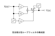
携帯電話機10においては、これらのループフィルタ109,126として、図9に示したLPFと同様に構成することもできるが、周波数オフセット、ランダム位相オフセットがある場合に最適フィルタとなる完全積分型のループフィルタとして構成することもできる。
【0131】
図10(A)に示す完全積分型のループフィルタの等価回路を同図(B)に示す。このループフィルタにおける伝達関数F(s)は、
F(s)=(1−sτ2)/(sτ1)、τ1=R1C、τ2=R2C
である。これを差分近似すると、入力信号X[n]と出力信号Y[n]との関係は、
Y[n]=Y[n−1]+a(X[n]−X[n−1])+bX[n]、
a=τ2/τ1、b=T/τ1
となる。ここで、Tはサンプリング周期であり、サンプリング周波数は、LPFのカットオフ周波数よりも十分高くする。上式より、ループフィルタで設定するパラメータは、a,bの2個となる。これらのパラメータa,bを、それぞれ、a=2A、b=2B(A,Bは整数)とすると、上式におけるaX[n]、aX[n−1]、bX[n]は、それぞれ、Aビット又はBビットだけ左シフトすることによって演算することができ、上式に示す演算は、図11に示すループフィルタによって実現することができる。
【0132】
したがって、ループフィルタにおいては、A,Bの値に対してCPU27による設定又は外部インターフェースを通じた設定を可能とした場合には、受信状況に応じて、当該ループフィルタの帯域幅及び応答速度を可変とすることができる。
【0133】
さらにまた、携帯電話機10においては、必要に応じて、同期捕捉部25におけるサンプラ71のサンプリングクロックを生成する手段としてNCOを用い、このNCOの周波数範囲も可変とする。
【0134】
すなわち、同期捕捉部25は、IF信号をサンプラ71によってC/Aコードの1周期である1ミリ秒の間に2046点以上の整数でサンプリングする必要がある。そのため、同期捕捉部25は、本件出願人が先に出願している特願2001−190658号及び特願2001−203193号に記載したように、2のべき乗個のサンプリング数でもってFFT処理を行うのが都合がよい。そこで、同期捕捉部25は、IF信号をサンプリングするためのサンプラ71をTCXO13から供給される発振信号D2に基づいて動作するNCOを用いて構成し、コスタスループ101及びDLL102と同様に、NCOに与えられる分周比を、集積回路端子の設定、CPU27による設定又は外部インターフェースを通じた設定を可変的に行うことによって任意のサンプリングクロックを実現することができる。
【0135】
以上のように、携帯電話機10においては、少なくとも周波数変換部24における周波数シンセサイザ19並びにコスタスループ101及びDLL102におけるNCO104,127の動作クロックを共用し、これらの周波数シンセサイザ19及びNCO104,127を、集積回路端子、CPU27又は外部インターフェースを通じて可変的に設定を行うことができるように構成するとともに、必要に応じて、周波数変換部24におけるLPF22、コスタスループ101及びDLL102におけるLPF107,108,117,118,122,123、及びコスタスループ101及びDLL102におけるループフィルタ109,126といった各種ディジタルフィルタ又はアナログフィルタや、同期捕捉部25におけるサンプラ71に設けられるNCOを、集積回路端子、CPU27又は外部インターフェースを通じて可変的に設定を行うことができるように構成することにより、TCXO13の発振周波数FOSCに左右されないGPS受信機の機能を組み込むことが可能となる。また、携帯電話機10においては、電話ユニット11とTCXO13を共用することにより、必要な発振器の個数を削減することができる。
【0136】
以下では、設定を可変とする上述した各部及びこれら以外の各部における具体的説明を行う。
【0137】
まず、周波数変換部24について説明する。
【0138】
周波数変換部24におけるLPF22(BPFでも可)は、アナログ的な構成をとることが殆どであることから、その特性は固定である場合が多い。携帯電話機10においては、中間周波数FIFに合わせてLPF22の通過周波数帯域等の特性を決定することから、復調回路31、すなわち、GPSユニットを先に図1に示した構成とし、TCXO13の発振周波数FOSCによらず中間周波数FIFがほぼ同じ周波数となるように、周波数変換部24における周波数シンセサイザ19の分周比を設定すれば問題はない。なお、携帯電話機10においては、特性が固定である場合のLPF22の観点からすると、中間周波数FIFの範囲は帯域外とならない程度に幅があってもよい。携帯電話機10においては、中間周波数FIFの範囲がTCXO13の発振周波数FOSCによらず目的の周波数に近い値に設定できるようにするには、上述した設定値K1の値を大きくし、位相比較器132による位相比較を行うリファレンスクロックの周波数を下げればよい。
【0139】
先に図8に示した周波数シンセサイザ19においては、リファレンスクロックをTCXO13の出力とし、TCXO13の発振周波数FOSCが18.414MHzである場合であって、例えば、上述した設定値K1,K2,K3,K4の値が、それぞれ、K1=18,K2=100,K3=15,K4=39の場合には、中間周波数FIFは1.023MHzとなり、設定値K1,K2,K3,K4の値が、それぞれ、K1=20,K2=100,K3=31,K4=49の場合には、中間周波数FIFは0.92MHzとなる。この例では、両者の間で中間周波数FIFの差が100kHz程度であることから、携帯電話機10においては、LPF22として通常のLPFを用いれば、両者の間で特性に差が生じることは特にない。
【0140】
また、周波数シンセサイザ19は、ベースバンド処理部やCPU等を含むディジタル信号処理を行う部分ではなく、アナログ信号処理を行うものとして設けられるのが通常であるが、分周器自体はディジタル信号処理を行うものである。そのため、携帯電話機10は、周波数シンセサイザ19における各分周器を上述したレジスタ138に設定された設定値に応じて分周するものとすることにより、集積回路端子、CPU27又は外部インターフェースを通じて分周比を可変的に設定することが可能となる。
【0141】
なお、携帯電話機10においては、上述したように、レジスタ138に対する設定値の設定を、集積回路端子、CPU27又は外部インターフェースを通じて行うが、レジスタ138に対する設定値の設定用のビット数が多い場合には、周波数シンセサイザ19を含む周波数変換部24とCPU27を含むベースバンド処理部とを接続するために必要なピン数が増加し、集積回路化する際には好ましくない。そこで、携帯電話機10においては、CPU27によってレジスタ138に対する設定値の読み出し及び書き込みを行う際に、所定の通信プロトコルに基づいたシリアル伝送を行うことにより、周波数シンセサイザ19を含む周波数変換部24とCPU27を含むベースバンド処理部とを接続するために必要なピン数を削減することができる。
【0142】
つぎに、ベースバンド処理部におけるDLL102に設けられるNCO127について説明する。
【0143】
携帯電話機10においては、RF信号がスペクトラム拡散信号であるため、拡散符号の同期を行うためのDLL102は、NCO127が拡散符号であるC/Aコードのチップレートである1.023MHz付近をカバーするように、TCXO13の発振周波数FOSCに応じて分周比を設定する。ここで、NCO127は、例えば図12に示すように構成することができる。
【0144】
すなわち、NCO127は、同図に示すように、TCXO13から供給される発振信号D2を所定の分周比で分周する分周器151,152と、後述するレジスタ155に保持される値の分解能を表すKビットのレジスタ値が設定されるレジスタ値設定部153と、このレジスタ値設定部153に設定されたレジスタ値とレジスタ155から読み出された値とを累積加算する加算器154と、この加算器154から供給される累積加算値を保持する有限長のレジスタ155と、分周器152から供給される分周された発振信号を所定の分周比で分周する分周器156と、CPU27によって設定された設定値N,M1,M2,M3を保持するレジスタやメモリ等の記憶素子157とを有する。
【0145】
分周器151は、TCXO13から供給される発振信号D2を、CPU27によって記憶素子157に設定された設定値M1を用いて表される分周比1/M1で分周する。分周器151は、分周した信号をレジスタ155に供給する。
【0146】
分周器152は、レジスタ155から読み出された値に応じて、TCXO13から供給される発振信号D2を、CPU27によって記憶素子157に設定された設定値M2を用いて表される分周比1/(M2−1)又は分周比1/M2又は分周比1/(M2+1)で分周する。分周器152は、分周した信号を分周器156に供給する。
【0147】
レジスタ値設定部153には、CPU27によって記憶素子157に設定された設定値Nが、レジスタ155に保持される値の分解能を表すKビットのレジスタ値として設定される。このレジスタ値Nは、2の補数で表され、正負の値をとるものである。レジスタ値設定部153に設定されたレジスタ値Nは、加算器154に供給される。
【0148】
加算器154は、レジスタ値設定部153に設定されたレジスタ値Nとレジスタ155から読み出された値とを加算する。加算器154は、加算して得られた累積加算値をレジスタ155に供給する。その結果、レジスタ155に保持される値は、レジスタ値Nの累積加算値となる。
【0149】
レジスタ155は、Kビットの有限長からなり、分周器151から供給される分周された発振信号をゲート信号としたタイミングに基づいて、加算器154から供給された累積加算値を保持する。このレジスタ155に保持された累積加算値は、分周器152における分周比を決定するのに用いられる。
【0150】
分周器156は、分周器152から供給される発振信号を、CPU27によって記憶素子157に設定された設定値M3を用いて表される分周比1/M3で分周する。分周器156は、分周した信号を再生キャリアとして出力する。
【0151】
記憶素子157は、CPU27によって設定された少なくとも4つの設定値N,M1,M2,M3を保持する。この記憶素子157に保持された設定値Nは、上述したように、レジスタ値設定部153に設定されるレジスタ値として用いられ、設定値M1は、分周器151における分周比を決定するのに用いられ、設定値M2は、分周器152における分周比を決定するのに用いられ、設定値M3は、分周器153における分周比を決定するのに用いられる。
【0152】
このようなNCO127は、4つの設定値N,M1,M2,M3を固定値とするのではなく、CPU27によって可変的に設定されるものとする。これにより、NCO127においては、周波数及び可変幅を設定することができる。ここで、NCO127においては、レジスタ155が有限長であることから、桁あふれが生じる場合がある。そこで、NCO127においては、レジスタ値設定部153に設定されたレジスタ値Nを加算器154によって累積加算していく際に、レジスタ155に保持される値の桁あふれがない場合には、分周器152によって分周比1/M2で分周するが、正の桁あふれが生じた場合には、分周器152の図示しないカウンタを"1"だけ多くカウントアップすることによって分周比1/(M2+1)で分周し、負の桁あふれが生じた場合には、分周器152のカウントアップを"1"だけ少なくすることによって分周比1/(M2−1)で分周する。したがって、NCO127は、レジスタ値設定部153に設定されるレジスタ値がN=0とされた場合には、TCXO13から供給される発振信号D2の発振周波数FOSCを1/(M2×M3)倍した周波数を有する再生キャリアを出力し、レジスタ値がN>0とされた場合には、レジスタ値がN=0とされた場合よりも高い周波数を有する再生キャリアを出力し、レジスタ値がN<0とされた場合には、レジスタ値がN=0とされた場合よりも低い周波数を有する再生キャリアを出力する。
【0153】
また、NCO127の周波数範囲は、拡散符号のチップレートにTCXO13の発振周波数FOSCの誤差と、送信側であるGPS衛星と受信側との相対速度の変化によって生じるドップラシフト量とを加えた範囲をカバーするように設定する。例えば、携帯電話機10においては、TCXO13を用いるものとすると、その発振周波数誤差が±約3ppm以内であれば、ドップラシフト量が±約3ppm以内であることから、全体としてNCO127の可変範囲が少なくとも1.023MHz±6ppm程度を含むものであればよい。
【0154】
つぎに、ベースバンド処理部におけるコスタスループ101に設けられるNCO104について説明する。
【0155】
RF信号は、例えば2相位相変調方式(Binary Phase Shift Keying;以下、BPSK変調方式という。)といったPSK変調方式に基づいて変調した信号又はPSK変調方式に基づいて変調した信号をスペクトラム拡散した信号であるが、IF信号におけるPSK信号のキャリアの同期を行うためのコスタスループ101は、NCO104が例えば周波数変換部24の設定によって1.023MHzとされる中間周波数FIF付近をカバーするように、TCXO13の発振周波数FOSCに応じて分周比を設定する。ここで、NCO104は、先に図12に示したNCO127と同様に構成することができる。
【0156】
NCO104の周波数範囲は、NCO127と同様に、中間周波数FIFにTCXO13の発振周波数FOSCの誤差と、送信側であるGPS衛星と受信側との相対速度の変化によって生じるドップラシフト量とを加えた範囲をカバーするように設定する。例えば、携帯電話機10においては、TCXO13を用いるものとすると、上述したように、その発振周波数誤差が±約3ppm以内であれば、ドップラシフト量が±約3ppm以内である。そのため、携帯電話機10においては、周波数変換部24によって1回でRF信号のキャリア周波数FRFを中間周波数FIFに変換する場合には、局部発振周波数FLOが周波数シンセサイザ19のリファレンスクロック周波数のL倍(Lは整数)とすれば、TCXO13の発振周波数FOSCの誤差による中間周波数FIFの誤差がL倍となることから、NCO104の可変範囲が少なくとも1.023MHz±3Lppm±3ppm程度を含むものであればよい。
【0157】
つぎに、ベースバンド処理部における同期捕捉部25に設けられるサンプラ71について説明する。
【0158】
携帯電話機10においては、同期捕捉部25を先に図3に示したように構成し、この同期捕捉部25によってスペクトラム拡散信号の拡散符号と同期をとるためのディジタルマッチドフィルタ処理を行う場合には、上述したように、IF信号をサンプラ71によってC/Aコードの1周期である1ミリ秒の間に2046点以上の整数でサンプリングする必要がある。ここで、携帯電話機10においては、IF信号をサンプリングするためのサンプリングクロックをTCXO13の発振周波数FOSCに基づいて生成するが、発振周波数FOSCによってサンプリング数が異なると、ディジタルマッチドフィルタ処理を行いにくくなる。
【0159】
しかしながら、携帯電話機10においては、先に図12に示したNCO127と同様の構成からなるNCOを用いてサンプラ71を構成してサンプリングクロックを生成させ、TCXO13の発振周波数FOSCに応じて、1ミリ秒あたりのサンプリング数が一定の整数値となるように、すなわち、一定のサンプリングレートとなるようにNCOを設定する。これにより、携帯電話機10においては、TCXO13の発振周波数FOSCに拘泥せずに、例えばソフトウェアで処理する場合にはディジタルマッチドフィルタ処理を同じ手順で行うことができる。
【0160】
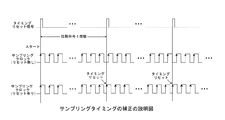
ところで、単純にサンプリングクロックをNCOによってのみ生成した場合には、TCXO13の発振周波数FOSCとNCOの周波数分解能との関係により、例えば図13中2段目に示すように、サンプリングする時間長によっては拡散符号の1周期あたりのサンプリング数に端数を生じ、タイミングが時間の経過とともにずれていく事態を生じ得る。この現象は、拡散符号の多周期にわたって信号処理を行う場合には好ましくないものである。この現象を回避するためには、NCOの周波数分解能を極めて高いものとする必要がある。
【0161】
そこで、携帯電話機10においては、例えば、同図中1段目に示すように、所定のタイミング信号生成手段によって拡散符号の1周期にほぼ一致するパルス状の周期的なタイミングリセット信号を生成し、同図中3段目に示すように、サンプリングクロックを生成させるサンプラ71におけるNCOを構成する先に図12に示した各分周器151,152,156とレジスタ155とをタイミングリセット信号に応じて1周期毎にリセットするといった動作を行うことにより、サンプリングするタイミングを初期化する。これにより、携帯電話機10においては、拡散符号の1周期におけるサンプリング数を常に同じものとし、且つ、サンプリングが行われるタイミングを各周期毎にほぼ同じものとすることができる。この場合、携帯電話機10においては、拡散符号の1周期内で生じた端数に起因して当該1周期の最後の部分でサンプリング間隔がずれるが、1周期毎にサンプリングのタイミングが補正されることから、NCOの周波数分解能を極めて高いものとする必要がない。
【0162】
ここで、携帯電話機10においては、拡散符号であるC/Aコードの周期に応じて、TCXO13の発振周波数FOSCの最小桁が決定される。すなわち、携帯電話機10においては、拡散符号であるC/Aコードの周期が1ミリ秒であることから、TCXO13の発振周波数FOSCの最小桁が1kHzであれば、NCOによって1周期にほぼ一致する周期的なタイミングリセット信号を容易に生成することができる。また、携帯電話機10においては、拡散符号の1周期である1ミリ秒間隔で、すなわち、1kHzのタイミングリセット信号を生成することにより、これらの処理を容易に行うことができる。したがって、携帯電話機10においては、TCXO13の発振周波数FOSCをある範囲内で自由度を持たせながらも最小桁を1kHzと指定することにより、例えばTCXO13の発振周波数FOSCが18.414MHzである場合には分周比を1/18414とする分周器を有するNCOによって容易に1ミリ秒間隔のタイミングリセット信号を生成することができる。
【0163】
なお、ここでは、発振周波数FOSCの最小桁を1kHzとするものとして説明したが、携帯電話機10においては、発振周波数FOSCの最小桁を1kHzの整数分の1としてもよい。この場合、携帯電話機10においては、1ミリ秒の整数倍間隔のタイミングリセット信号を生成することができ、例えばTCXO13の発振周波数FOSCが18.4145MHzである場合には分周比を1/336829とした分周器を有するNCOによって2ミリ秒間隔で、すなわち、C/Aコードの2周期長のタイミングリセット信号を生成することができる。このとき、携帯電話機10においては、拡散符号の1周期あたりのサンプリング数を一定の整数値とする上述した処理を、1周期長から2周期長に置き換え、FFT等の処理を2周期長のデータ単位で行うか、或いはデータを半分長ずつに分けて1周期長での処理を行うといったようにする。これにより、携帯電話機10においては、処理内容が若干増加するものの、C/Aコードの周期を単位とすることで処理がしやすくなる。
【0164】
また、携帯電話機10においては、ディジタルマッチドフィルタ処理が先に図2に示したFFTを利用したものである場合には、サンプリング数が2のべき乗個であることがFFT処理には都合がよいことから、TCXO13の発振周波数FOSCによって拡散符号の1周期あたりのサンプリング数が2のべき乗個となるようにサンプラ71を設定することにより、処理が極めて容易となる。
【0165】
さらに、携帯電話機10においては、拡散符号がいわゆるM系列又はM系列から生成されるいわゆるGold符号である場合には、符号長が2のべき乗−1であることから、TCXO13の発振周波数FOSCによってはサンプリング数を拡散符号の1周期あたり(2のべき乗−1)個とする方が容易な場合がある。ここで、ディジタルマッチドフィルタ処理が先に図2に示したFFTを利用したものである場合には、上述したように、サンプリング数が2のべき乗個であることが好ましいことから、携帯電話機10においては、符号長が2のべき乗−1である拡散符号を処理する場合には、拡散符号の1周期の中でダミーのビットを等間隔で挿入し、FFT処理を行うデータ数を2のべき乗個に合わせ込むようにしてもよい。
【0166】
例えば、携帯電話機10においては、C/Aコードの1周期である1ミリ秒で4092個のサンプリングを行った場合には、1/4周期、すなわち、1023個のサンプリングを行う毎に、1個のダミーデータを挿入すればよい。このとき、挿入するダミーデータは、当該ダミーデータの直前のビットと同じ値とするのが自然であるが、固定値としてもよい。
【0167】
なお、携帯電話機10においては、ディジタルマッチドフィルタ処理をソフトウェアとして実装する場合であって処理能力に余裕がある場合には、FFT処理を行う場合であっても、拡散符号の1周期あたりのサンプリング数を必ずしも2のべき乗個にする必要はなく、サンプリング数がある程度多めになるようにサンプラ71におけるNCOを設定し、ソフトウェアで処理する際に2のべき乗個となるように間引きしてから、間引きしたデータに対してFFT処理を行うようにしてもよい。
【0168】
つぎに、ベースバンド処理部又は周波数変換部24におけるLPFを含む各フィルタについて説明する。
【0169】
LPFを例えば先に図9(A)に示したようなディジタルフィルタとして構成した場合には、当該LPFの帯域は、多段階に設定することができる。同図に示すLPFにおいては、上述したように、サンプリング周波数をfsとすると、時定数tc、カットオフ周波数fcは、それぞれ、
tc=RC=1/(kfs)、
fc=1/(2πRC)=kfs/(2π)、
k=1/(RCfs)
となる。ここで、サンプリング周波数fsとTCXO13の発振周波数FOSCとが等しいものとすると、カットオフ周波数fcは、TCXO13の発振周波数FOSCに比例して変化するものとなる。
【0170】
したがって、このようなLPFを先に図5に示したコスタスループ101に適用した場合には、サンプリング周波数をfs=20MHzとすると、カットオフ周波数fcは、48.6Hzとなり、サンプリング周波数をfs=10MHzとすると、カットオフ周波数fcは、24.3Hzとなる。ここで、データの伝送速度が50bpsであり、且つ、NRZ(Non Return to Zero)信号であるGPS衛星からの信号に含まれるメッセージの主帯域幅が25Hzであるものとし、これを考慮すると、サンプリング周波数をfs=10MHzとした場合のカットオフ周波数fcである24.3Hzは、若干狭い。そこで、携帯電話機10においては、サンプリング周波数をfs=10MHzとした場合には、カットオフ周波数fcを1つ上げるようにする。
【0171】
また、携帯電話機10においては、LPFとして、先に図9(A)に示したもの以外にも、有限インパルス応答(Finite Impulse Response;FIR)フィルタや、他の構成のIIRフィルタを用いることも可能である。また、携帯電話機10においては、コスタスループ101以外の各部であっても、先に図1に示した周波数変換部24におけるA/D23の後段にLPFを配置することによって当該LPFをディジタルフィルタとして構成することもできる。さらに、携帯電話機10においては、LPFの代わりに中間周波数FIF付近を帯域の中心としたBPFを適用することもできる。携帯電話機10においては、LPF又はBPFを適用した場合であっても、中間周波数FIFがほぼ一定範囲に収まるように周波数シンセサイザ19を構成すると、TCXO13の発振周波数FOSCによってフィルタの帯域が変化することから、フィルタの帯域を可変としておくことはこのような場合にも有効である。
【0172】
このように、携帯電話機10においては、フィルタの帯域を可変可能とし、TCXO13の発振周波数FOSCに応じて、フィルタの設定を変化させることにより、フィルタの帯域を最適とした動作を行うことができる。
【0173】
ところで、携帯電話機10は、上述したように、GPS衛星からのスペクトラム拡散信号における拡散符号である1ミリ秒周期のC/Aコードの同期タイミングを計測することによって測位演算を行い、自己の位置を取得するものである。ここで、拡散符号の同期タイミングを計測するにあたっての計測の時間分解能は、上述した同期捕捉部25といった同期回路の動作クロック周波数に依存する。したがって、携帯電話機10においては、同期回路の動作クロックをTCXO13によって生成する場合には、計測の時間分解能はTCXO13の発振周波数FOSCに依存することになる。
【0174】
通常、GPS受信機においては、内部に設けられる時計に同期した基準タイミングを起点として、そこからC/Aコードの先頭がどれだけ遅延した位置に現れるかをカウンタによって計測し、当該GPS受信機の時計を基準にしたGPS衛星から当該GPS受信機までの電波の到達距離である擬似距離を算出する。ここで、GPS受信機においては、電波の到達時間が同一であっても、TCXO等の源発振器の発振周波数が異なればカウント値も異なることになる。
【0175】
そこで、携帯電話機10は、例えば先に図1に示したCPU27によってTCXO13の発振周波数FOSCに応じてカウント値を時間に換算する。これにより、携帯電話機10は、TCXO13の発振周波数FOSCが変化した場合であっても、正確な擬似距離の算出に容易に対応することができる。
【0176】
さて、これまでは、GPS衛星からの信号を含むスペクトラム拡散信号の復調回路及びGPS受信機の復調に関する部分についての対応について説明してきたが、携帯電話機10は、これら以外の各部についても、TCXO13の発振周波数FOSCに対する対応を施す。
【0177】
GPS受信機は、一般に、外部との通信等を行うために、例えば、所定のシリアルポートやUSB(Universal Serial Bus)ポート等の各種入出力インターフェース、上述したタイマ29のような制御用のタイマ、A/D、及びディジタル/アナログ変換器(Digital/Analog Converter;以下、D/Aという。)等の各種ペリフェラルを内蔵する。GPS受信機においては、これら各部の動作クロックも、周波数変換や同期を行う各部と同じ源発振器から生成するのが通常である。
【0178】
そこで、携帯電話機10においては、TCXO13の発振周波数FOSCにより、通信速度、時間及びサンプリング周波数等に影響が及ぶことから、発振周波数FOSCに応じて、各種入出力インターフェースの通信速度、タイマ29、並びにA/D及び/又はD/Aのサンプリング周波数の設定を変えるようにする。これにより、携帯電話機10は、各種ペリフェラルについても、TCXO13の発振周波数FOSCに拘泥せずに動作させることができる。
【0179】
以上のように、携帯電話機10は、GPSユニットに必要となる発振器を、本来であれば電話ユニット11のために設けられたTCXO13と共用し、TCXO13の発振周波数FOSCに応じて各部の設定を変更することにより、発振周波数FOSCの変化に依存しない動作を行うことができ、GPSユニットのための専用の発振器を設ける必要がないことから、発振器の個数を削減することができる。すなわち、携帯電話機10は、特定の周波数を発振しない源発振器を用いた場合であっても、源発振器の発振周波数に応じて各部の設定を可変とすることにより、発振周波数の変化に依存しない動作を行うことができ、発振器の個数を削減することができる。
【0180】
なお、携帯電話機11においては、電話ユニット11の他、例えばいわゆるブルートゥース(Bluetooth(登録商標))や無線LAN(Local Area Network)等の所定の無線システムに対応する無線ユニットが同じモジュール又は機器に搭載されている場合には、無線ユニット用又は信号処理用に当該無線ユニットが対応する無線の種別に応じた周波数を発振する発振器が存在することになる。この場合、携帯電話機10においては、無線ユニット用又は信号処理用に設けられる発振器をGPSユニットの源発振器とするようにしてもよい。勿論、携帯電話機10は、無線ユニット以外の他の機能を実現するユニットが搭載されている場合には、このユニット用に設けられる発振器をGPSユニットの源発振器とするようにしてもよい。
【0181】
ところで、携帯電話機10においては、TCXO13の発振周波数FOSCに応じた設定変更の対象として、上述したように、少なくとも周波数変換部24における周波数シンセサイザ19の分周比並びにコスタスループ101及びDLL102におけるNCO104,127の周波数範囲の他、必要に応じて、LPF等の各フィルタの特性、同期捕捉部25におけるサンプラ71のサンプリングクロック、及びその他の各種ペリフェラルがある。このように、携帯電話機10においては、TCXO13の発振周波数FOSCに応じて設定を可変とすべき箇所が多い。そのため、携帯電話機10においては、各部の最適な設定値を算出し、得られた各設定値を所定の外部インターフェース等を介して設定するのは煩雑である。
【0182】
そこで、携帯電話機10においては、TCXO13の発振周波数FOSCに応じた各設定値を算出するルーチンをCPU27が実行可能なプログラムとして内蔵しておき、外部インターフェースからはTCXO13の発振周波数FOSCのみを入力するとともに、入力した発振周波数FOSCに基づいてCPU27によって各設定値を算出し、CPU27によって各設定値を各部に対して自動的に設定することにより、設定の煩雑さを解消することができる。
【0183】
また、携帯電話機10においては、例えば上述したRTC28に対する動作クロックを供給するための32.768kHz程度の所定の発振周波数を有する発振信号を生成する上述したXO12といった他の既知周波数の発振器を備えている場合には、この発振器によって生成される発振信号をゲート信号として、ある一定期間で源発振器たるTCXO13からの出力パルスを簡易的にカウントする機能を持たせることにより、このカウント値に基づいて、おおよその発振周波数FOSCを当該携帯電話機10が把握することが可能となる。具体的には、携帯電話機10においては、XO12の精度を仮に±100ppmとすると、例えば10〜20MHz程度の周波数範囲を許容するTCXO13に対しては約±100ppmの精度、すなわち、約±1〜2kHzの誤差範囲で、TCXO13の発振周波数FOSCを推定することができる。また、携帯電話機10においては、XO12の精度がさらによい場合には、1kHz単位でのTCXO13の発振周波数FOSCの特定を行うことも十分可能となる。
【0184】
一般に利用される源発振器の発振周波数は、実際にはそれほど種類が多くはないことから、精度は高くなくともおおよその値を把握することができるならば、例えば、利用可能なTCXO13の発振周波数FOSCのテーブルを予めメモリ30に記憶させておくことにより、どの発振周波数の発振器かを確実に判別することができる。したがって、携帯電話機10においては、このような機能を当該携帯電話機10の電源がオン状態となると同時に作動するようにCPU27の初期ルーチンとして内蔵しておき、CPU27によってTCXO13の発振周波数FOSCを特定できるならば、CPU27による上述した各部に対する各設定値の設定動作と組み合わせることにより、完全に自動的に周波数変換部24における周波数シンセサイザ19、コスタスループ101及びDLL102におけるNCO104,127、LPF等の各フィルタ、同期捕捉部25におけるサンプラ71、及びその他の各種ペリフェラルに対する設定を行うことが可能となる。なお、携帯電話機10においては、ペリフェラルに関しては、通信速度が設定されない状態では外部からの制御が困難であることから、外部との入出力インターフェースの通信速度を自動設定することにより、外部との通信が可能となることは重要である。
【0185】
以上説明したように、携帯電話機10に組み込まれるGPSユニットにおいては、必要となるクロックの発振周波数が特定の周波数である必要がなくなることから、TCXO13等の大量に市販されている標準的な発振器を利用することができる。
【0186】
また、GPSユニットにおいては、必要な源発振器として、携帯電話機10等の電子機器に組み込む際に、本来であれば電話ユニット11といった他の機能を実現するユニットのために設けられたTCXO13等の発振器と共用することができ、当該GPSユニットのための専用の発振器を設ける必要がないことから、電子機器に搭載される発振器の個数を削減してコストダウン及び小型化を図ることができる。
【0187】
さらに、GPSユニットは、モジュール化又は上述した復調回路31のように集積回路化して構成する場合には、様々な源発振器が設けられた場合、すなわち、TCXO13の発振周波数FOSCが多様であっても、1種類のモジュール又は集積回路で対応することができる。したがって、GPSユニットは、様々な発振周波数の電子機器に搭載することができる汎用品として流通させることが可能となる。
【0188】
さらにまた、GPSユニットは、RF信号の周波数FRF及びIF信号の周波数FIFを可変とすることができることから、複数の無線周波数に対応することが可能となる。
【0189】
なお、本発明は、上述した実施の形態に限定されるものではない。例えば、上述した実施の形態では、GPS受信機の機能を実現するGPSユニットが組み込まれた携帯電話機10を用いて説明したが、本発明は、携帯電話機以外の電子機器にも容易に適用することができ、また、GPSユニット以外の他の機能を実現するユニットが組み込まれた電子機器であっても容易に適用することができる。
【0190】
また、上述した実施の形態では、スペクトラム拡散信号を復調するものとして説明したが、本発明は、スペクトラム拡散信号以外であっても、所定の高周波の信号を復調するものであれば、いかなるものでも適用することができる。
【0191】
さらに、上述した実施の形態では、GPS受信機の機能を実現するGPSユニットが組み込まれた携帯電話機10を用いて説明したが、本発明は、衛星を利用した測位システム、すなわち、GNSSシステムを適用した受信機の機能が組み込まれた電子機器であれば、いかなるものであっても適用することができる。GNSSシステムとしては、米国における上述したGPSシステムの他、旧ソ連邦におけるGLONASS(Global Navigation Satellites System)や、欧州を中心として開発が進められているGALILEO等があるが、本発明は、これら全てのGNSSシステムを適用することができるものである。
【0192】
このように、本発明は、その趣旨を逸脱しない範囲で適宜変更が可能であることはいうまでもない。
【0193】
【発明の効果】
以上詳細に説明したように、本発明にかかる復調装置は、所定の高周波信号を復調する復調装置であって、高周波信号の周波数を所定の中間周波数に変換する周波数変換手段と、この周波数変換手段によって得られた中間周波数を有する中間周波数信号に対する所定の信号処理を施す信号処理手段と、周波数変換手段及び信号処理手段に対する設定を行う設定手段とを備え、周波数変換手段は、所定の源発振器によって生成される所定の源発振信号に基づいて、高周波信号の周波数を所定の中間周波数に変換するための局部発振周波数を有する局部発振信号を生成する局部発振信号生成手段を有し、信号処理手段は、局部発振信号生成手段と源発振器を共用し、源発振器によって生成される源発振信号に基づいて、所定の周波数を有する信号を生成する信号生成手段を有し、局部発振信号生成手段は、源発振信号の源発振周波数に拘泥せずに中間周波数が所定の範囲内の値となるように、源発振器によって生成される源発振信号の任意の源発振周波数に応じて、設定手段を介して分周比が可変的に設定されることによって局部発振信号の局部発振周波数を可変とし、信号生成手段は、源発振器によって生成される源発振信号の任意の源発振周波数に応じて、設定手段を介して分周比が可変的に設定されることによって信号の周波数を可変とする。
【0194】
したがって、本発明にかかる復調装置は、少なくとも局部発振信号生成手段と信号生成手段との源発振器を共用し、源発振信号の源発振周波数に拘泥せずに中間周波数が所定の範囲内の値となるように、任意の源発振周波数に応じて、少なくとも局部発振信号生成手段と信号生成手段との分周比が設定手段を介して可変的に設定されることにより、様々な発振周波数に対応することができ、必要となる源発振周波数が特定の周波数である必要がなくなることから、源発振器として標準的な発振器を利用することができる。
【0195】
また、本発明にかかる受信装置は、衛星からの信号を受信して自己の位置及び速度を算出する測位ユニットが組み込まれた受信装置であって、衛星からの信号を受信する受信手段と、この受信手段によって受信した所定の高周波信号の周波数を所定の中間周波数に変換する周波数変換手段と、この周波数変換手段によって得られた中間周波数を有する中間周波数信号に対する所定の信号処理を施す信号処理手段と、周波数変換手段及び信号処理手段に対する設定を行う設定手段と、測位ユニットとは異なる所定の機能を実現する他のユニットの動作クロックを生成するために設けられ、所定の源発振信号を有する源発振信号を生成する源発振器とを備え、周波数変換手段は、源発振器によって生成される源発振信号に基づいて、高周波信号の周波数を中間周波数に変換するための局部発振周波数を有する局部発振信号を生成する局部発振信号生成手段を有し、信号処理手段は、局部発振信号生成手段と源発振器を共用し、源発振器によって生成される源発振信号に基づいて、所定の周波数を有する信号を生成する信号生成手段を有し、局部発振信号生成手段は、源発振信号の源発振周波数に拘泥せずに中間周波数が所定の範囲内の値となるように、源発振器によって生成される源発振信号の任意の源発振周波数に応じて、設定手段を介して分周比が可変的に設定されることによって局部発振信号の局部発振周波数を可変とし、信号生成手段は、源発振器によって生成される源発振信号の任意の源発振周波数に応じて、設定手段を介して分周比が可変的に設定されることによって信号の周波数を可変とする。
【0196】
したがって、本発明にかかる受信装置は、測位ユニットにおける少なくとも局部発振信号生成手段と信号生成手段との源発振器を共用するとともに、この源発振器として、測位ユニットとは異なる所定の機能を実現する他のユニットの動作クロックを生成するために設けられた源発振器を共用し、源発振信号の源発振周波数に拘泥せずに中間周波数が所定の範囲内の値となるように、任意の源発振周波数に応じて、少なくとも局部発振信号生成手段と信号生成手段との分周比が設定手段を介して可変的に設定されることにより、様々な発振周波数に対応することができ、必要となる源発振周波数が特定の周波数である必要がなくなることから、源発振器として標準的な発振器を利用することができる、また、所定の機能を有する電子機器に既に搭載されている発振器からの発振周波数を源発振周波数として利用することによってコストダウン及び小型化を図ることができる。
【図面の簡単な説明】
【図1】本発明の実施の形態として示す携帯電話機の構成を説明するブロック図である。
【図2】同携帯電話機が備える同期捕捉部として適用することができるFFTを利用したディジタルマッチドフィルタの構成を説明するブロック図である。
【図3】同携帯電話機が備える同期捕捉部として図2に示すディジタルマッチドフィルタを適用した場合における実際の実装例を説明するブロック図である。
【図4】同携帯電話機が備える同期保持部の構成を説明するブロック図である。
【図5】同携帯電話機が備える同期保持部が有するチャンネル回路の構成を説明するブロック図である。
【図6】同携帯電話機が備える同期保持部における拡散符号の位相合わせについて説明するための図である。
【図7】同携帯電話機が備える同期保持部における拡散符号の位相補正について説明するための図である。
【図8】同携帯電話機が備える周波数変換部が有する周波数シンセサイザの構成を説明するブロック図である。
【図9】LPFの構成を説明する図であって、(A)は、IIRフィルタの構成を示し、(B)は、RCフィルタの構成を示す図である。
【図10】完全積分型のループフィルタの等価回路の構成を説明する図であって、(A)は、ループフィルタの構成を示し、(B)は、(A)に示すループフィルタの等価回路の構成を示す図である。
【図11】完全積分型のループフィルタの構成を説明する図である。
【図12】同携帯電話機が備える同期保持部が有するNCOの構成を説明するブロック図である。
【図13】同携帯電話機が備える同期捕捉部が有するサンプラにおけるサンプリングタイミングの補正について説明するための図である。
【図14】GPS衛星からの信号の構成を説明する図である。
【図15】従来の拡散符号及びキャリアの同期処理を説明するための図であって、周波数サーチを説明するための図である。
【図16】ディジタルマッチドフィルタを用いて検出した相関値の時間変化を示す出力波形の例を説明する図である。
【符号の説明】
10 携帯電話機、 11 電話ユニット、 12 XO、 13 TCXO、 14 逓倍/分周器、 15 アンテナ、 16 LNA、 17 BPF、 18,21 増幅器、 19 周波数シンセサイザ、 20 ミキサ、 22,107,108,117,118,122,123,133 LPF、 23 A/D、 24 周波数変換部、 25 同期捕捉部、 26 同期保持部、 27 CPU、 28 RTC、 29 タイマ、 30,52,54,57 メモリ、 31 復調回路、 50 ディジタルマッチドフィルタ、 51,71 サンプラ、 53,56 FFT処理部、 55,128 拡散符号発生器、 58,103,105,106,113,114,115,116,120,121,141,142 乗算器、 59 IFFT処理部、 60 ピーク検出器、 72 RAM、 73 RAM/ROM、 74 DSP、 81,811,812,・・・,81N チャンネル回路、 82 コントロール・レジスタ、 101 コスタスループ、 102 DLL、 104,127NCO、 109,126 ループフィルタ、 110,125 位相検出器、 111 2値化回路、 112,119,124 2乗和算出回路、 131,151,152,156 分周器、 132 位相比較器、 134 VCO、 135 パルススワロカウンタ、 136,137 ダウンカウンタ、 138,157 記憶素子、 143 差分器、 144,154 加算器、 145,155 レジスタ、 153 レジスタ値設定部[0001]
BACKGROUND OF THE INVENTION
The present invention is a demodulator that demodulates a predetermined high-frequency signal, and a receiver to which the demodulator is applied, and receives a signal from a satellite in a so-called GNSS (Global Navigation Satellites System) and calculates its position and velocity. The present invention relates to a receiving device.
[0002]
[Prior art]
In recent years, GNSS systems that measure the position of a moving object on the ground using an artificial satellite are becoming widespread. As this GNSS system, for example, there is a global positioning system (hereinafter referred to as GPS). In this GPS system, a GPS receiver that receives signals from GPS satellites receives signals from at least four GPS satellites, calculates the position of the GPS receiver based on the received signals, and It is a basic function to notify to.
[0003]
In other words, the GPS receiver demodulates the signal from each GPS satellite to obtain the orbit information of each GPS satellite, and based on the orbit and time information of each GPS satellite and the delay time of the received signal, the GPS receiver Is derived by simultaneous equations. In the GPS system, at least four GPS satellites for obtaining received signals are required because there is an error between the internal time due to the clock provided in the GPS receiver and the time due to the atomic clock provided in the GPS satellite. This is because the pseudo distances from at least four GPS satellites are necessary to calculate the four unknown parameters of the three-dimensional position and the accurate time from which the influence of the above is removed.
[0004]
In the GPS system, when a consumer GPS receiver is used, a spread spectrum signal radio wave called a C / A (Clear and Acquisition) code is received from the GPS satellite (Navstar) and positioning calculation is performed. Do.
[0005]
The transmission signal called the L1 band and C / A code has a transmission signal speed, that is, a chip rate of 1.023 MHz, and a pseudo-random noise (PN) having a code length of 1023 such as a so-called Gold code. ) Binary phase shift keying (hereinafter referred to as BPSK modulation method) with respect to a carrier having a frequency of 1575.42 MHz (hereinafter referred to as carrier) using a signal obtained by directly spreading 50 bps data with a sequence spreading code. It is a signal that has been modulated based on. In this case, since the code length is 1023, as shown in the first stage in FIG. 14, the C / A code has a spreading code of 1023 chips as one period, that is, one period = 1 millisecond (msec). Will be repeated.
[0006]
The spreading code of this C / A code is different for each GPS satellite, but which GPS satellite uses which spreading code can be detected in advance by a GPS receiver. Further, the GPS receiver can grasp which GPS satellite can receive a signal at that point and at that point by a navigation message described later. Therefore, for example, in the case of three-dimensional positioning, a GPS receiver receives radio waves from at least four or more GPS satellites that can be acquired at that point and at that time, performs spectrum despreading, and performs positioning calculation Thus, the position of itself is calculated.
[0007]
One bit of the signal data from the GPS satellite is transmitted for 20 cycles of the spread code, that is, in units of 20 milliseconds, as shown in the second stage in the figure. That is, the data transmission rate is 50 bps as described above. Further, 1023 chips for one cycle of the spread code are inverted when the bit is “1” and when it is “0”.
[0008]
Further, the signal from the GPS satellite forms one word with 30 bits, that is, 600 milliseconds, as shown in the third row in FIG. Furthermore, the signal from the GPS satellite forms one subframe in 10 words, that is, 6 seconds, as shown in the fourth row in FIG. In the signal from the GPS satellite, as shown in the fifth row in the figure, a preamble that always has a prescribed bit pattern is added to the first word of one subframe even when data is updated. Inserted, and data is transmitted following this preamble.
[0009]
Furthermore, signals from GPS satellites form 5 subframes, ie, 1 frame in 30 seconds. And in the signal from a GPS satellite, the navigation message mentioned above is transmitted in the data unit of this 1 frame.
[0010]
The first three subframes of the data of one frame are information specific to GPS satellites called ephemeris information. The ephemeris information includes a parameter for obtaining the orbit of the GPS satellite and a transmission time of the signal from the GPS satellite.
[0011]
All GPS satellites use the common time information by providing an atomic clock, and the transmission time of the signal from the GPS satellite included in the ephemeris information is in units of one second of the atomic clock. Further, the spread codes of GPS satellites are generated in synchronization with the atomic clock.
[0012]
The trajectory information included in the ephemeris information is updated every few hours, but is the same information until the update is performed. Therefore, the GPS receiver can use the same orbit information accurately for several hours by holding the orbit information included in the ephemeris information in the memory. Note that the signal transmission time from the GPS satellite is updated every 6 seconds as TOW (Time Of Week) information.
[0013]
On the other hand, the navigation messages of the remaining two subframes in one frame of data are information transmitted in common from all GPS satellites called almanac information. This almanac information is required for 25 frames in order to acquire all information, and is composed of approximate position information of each GPS satellite, information indicating which GPS satellite can be used, and the like. This almanac information is updated every few days, but is the same information until the update is performed. Therefore, the GPS receiver can use the same information accurately for several days by holding the almanac information in the memory. However, the GPS receiver can use the same almanac information for several months, although the accuracy is somewhat reduced.
[0014]
In order to receive the signal from the GPS satellite and obtain the above-mentioned data, the GPS receiver first removes the carrier and then uses the same spreading code as the C / A code used by the GPS satellite to be received. Using the signal from the GPS satellite, the signal from the GPS satellite is captured by phase-synchronizing the C / A code and the spectrum is despread. When the GPS receiver performs spectrum despreading in phase synchronization with the C / A code, bits are detected, and a navigation message including time information and the like can be acquired based on a signal from a GPS satellite. Become.
[0015]
The GPS receiver captures a signal from a GPS satellite by a phase-locked search of a C / A code. As this phase-locked search, a correlation between a spread code generated by itself and a spread code of a received signal from a GPS satellite is performed. For example, when the correlation value of the correlation detection result is larger than a predetermined value, it is determined that the two are synchronized. If the GPS receiver determines that synchronization is not achieved, it uses some synchronization technique to control the phase of the spreading code generated by itself and synchronize it with the spreading code of the received signal. Yes.
[0016]
By the way, as described above, the signal from the GPS satellite is a signal obtained by modulating the carrier based on the BPSK modulation method with the signal obtained by spreading the data with the spreading code. Therefore, in order to receive a signal from a GPS satellite, the GPS receiver needs to synchronize not only the spreading code but also the carrier and data, but cannot synchronize the spreading code and the carrier independently.
[0017]
The GPS receiver usually converts the received signal into an IF signal by converting the carrier frequency of the received signal into an intermediate frequency (hereinafter referred to as IF) within several MHz, and the IF signal is used to convert the received signal into the IF signal. Perform the synchronization detection process. The carrier in the IF signal (hereinafter referred to as IF carrier) mainly includes a frequency error due to Doppler shift according to the moving speed of the GPS satellite, and an internal part of the GPS receiver when the received signal is converted into an IF signal. The frequency error of the local oscillator generated by
[0018]
Therefore, in the GPS receiver, since the IF carrier frequency is unknown due to these frequency error factors, it is necessary to search for the frequency. In addition, since the synchronization point (synchronization phase) within one cycle of the spread code is unknown due to dependence on the positional relationship between the GPS receiver and the GPS satellite, the GPS receiver described above Thus, some kind of synchronization method is required.
[0019]
A conventional GPS receiver uses a synchronization method that combines a frequency search for a carrier, synchronization acquisition by a sliding correlator, and synchronization maintenance by a DLL (Delay Locked Loop) and a Costas loop. Hereinafter, this synchronization method will be described.
[0020]
As a clock for driving a spread code generator of a GPS receiver, a clock obtained by dividing a reference frequency oscillator prepared in the GPS receiver is generally used. A high-precision crystal oscillator is used as the reference frequency oscillator, and the GPS receiver uses a local oscillation signal used to convert a received signal from a GPS satellite into an IF signal based on the output of the reference frequency oscillator. Generate.
[0021]
Here, FIG. 15 shows the processing contents for the frequency search. The GPS receiver performs a phase synchronization search for a spread code when the frequency of the clock signal that drives the spread code generator is a certain frequency f1. That is, the GPS receiver detects the correlation between the received signal from the GPS satellite and the spreading code at each chip phase by sequentially shifting the phase of the spreading code by one chip, and detects the correlation peak. Thus, a phase that can be synchronized is detected. In addition, when the frequency of the clock signal is f1, the GPS receiver changes the frequency division ratio with respect to the reference frequency oscillator, for example, if there is no phase that is synchronized in all the phase searches for 1023 chips. The frequency of the signal is changed to another frequency f2, and the phase search for 1023 chips is similarly performed. The GPS receiver implements a frequency search by repeating such an operation by changing the frequency of the clock signal stepwise.
[0022]
When the GPS receiver detects the frequency of the clock signal that can be synchronized by performing such a frequency search, the GPS receiver performs phase synchronization of the final spread code at the frequency of the clock signal. As a result, the GPS receiver can capture a signal from a GPS satellite even when there is a deviation in the oscillation frequency of the crystal oscillator.
[0023]
However, such a conventional synchronization method is not suitable for high-speed synchronization in principle. In the GPS receiver, if it takes time to synchronize the spread code and the IF carrier, the reaction becomes slow and inconvenience occurs in use. Therefore, in an actual GPS receiver, in order to compensate for this disadvantage, the time until synchronization acquisition is shortened by parallel processing by increasing the number of channels.
[0024]
On the other hand, as a technique for performing high-speed acquisition of a spread spectrum signal instead of the above-described technique using sliding correlation, a matched filter is used. The matched filter can be digitally realized by a so-called transversal filter. In addition, as a matched filter, a spread code is obtained by a digital matched filter using a fast Fourier transform (hereinafter referred to as FFT) due to an improvement in hardware capability represented by a recent DSP (Digital Signal Processor). A technique for performing high-speed synchronization is realized. The latter is based on a correlation calculation speed-up method that has been known for a long time.
[0025]
By using these matched filters, the GPS receiver detects a correlation peak, for example, as shown in FIG. 16 for one period of the output waveform when there is a correlation. The position of this peak indicates the beginning of the spread code. By detecting this peak, the GPS receiver can acquire synchronization, that is, detect the phase of the spread code in the received signal. Further, the GPS receiver can detect the IF carrier frequency together with the phase of the spread code by using the above-described digital matched filter using FFT and performing an operation in the frequency domain of the FFT. Then, the GPS receiver converts the phase of the spread code into a pseudorange, and can calculate the position of the GPS receiver when at least four GPS satellites are detected. Based on this, the speed of the GPS receiver can be calculated.
[0026]
[Problems to be solved by the invention]
By the way, in the GPS receiver using the C / A code described above, a multiple of 1.023 MHz which is the chip rate of the C / A code is used as the source oscillation frequency which is the frequency of the oscillation signal generated by the oscillator described above. It is often done. For example, in the GPS receiver, when 16.368 MHz, which is 16 times the chip rate, is used as the source oscillation frequency, the operation clock of the digital signal processing unit that processes the baseband signal is the same frequency as that of the source oscillator. .368 MHz, the frequency of the local oscillation signal used to convert the received signal from the GPS satellite to the IF signal is 16.368 MHz × 96 = 1571.328 MHz, and the frequency of the IF signal is typically 4.092 MHz. It is. In this case, in the GPS receiver, if the source oscillation frequency is changed, the frequency of the IF signal changes greatly.
[0027]
For example, in a GPS receiver, when the source oscillation frequency is simply changed from 16.368 MHz to 16 MHz, the frequency of the IF signal is significantly changed to 39.42 MHz, which is difficult to handle in baseband processing. It becomes. As another example, in the GPS receiver, when the source oscillation frequency is changed to 16.4 MHz, the frequency of the IF signal is 1.02 MHz, which can be adequately handled by baseband processing. When the band pass filter (BPF) for conversion is fixed to a band centered on 4.092 MHz, the IF signal is greatly attenuated.
[0028]
In the GPS receiver, the above-described DLL and Costas loop for demodulating the spread spectrum signal, and the NCO (NCO based on the source oscillation frequency used for the sampling clock for accumulating the IF signal and sampling at a predetermined sampling frequency) The frequency range of the Numeric Controlled Oscillator will also change.
[0029]
As described above, in the GPS receiver, when the source oscillation frequency is changed, it is not possible to cope with the baseband processing.
[0030]
Here, as an example of using the GPS receiver, there is an example in which the function of the GPS receiver is incorporated in an electronic device having a predetermined function such as a portable terminal such as a cellular phone. In this case, since the electronic device is equipped with an oscillator that generates a signal having a different frequency for each clock, it is newly added for the GPS unit, which is a component for realizing the function of the GPS receiver. In addition to increasing the cost and increasing the size of electronic equipment, mounting an oscillator also increases EMC (Electro Magnetic).
From the viewpoint of compatibility, it is also a new unnecessary radiation source.
[0031]
Therefore, in the electronic device, it is preferable that the clock for the GPS unit is also obtained from an oscillator mounted on the electronic device. However, since the frequency of the oscillator varies depending on the electronic device, the GPS unit is designed with a frequency converter and other digital signal processors that downconvert the received signal to an IF signal so that any oscillation frequency can be supported. Need to be.
[0032]
These problems are not limited to the function of the GPS receiver, but are common when various units that realize a predetermined function other than the function of the GPS receiver are incorporated in a predetermined electronic device.
[0033]
The present invention has been made in view of such circumstances, and can deal with various oscillation frequencies, and can also generate an oscillation frequency from an oscillator already mounted on an electronic device having a predetermined function. An object of the present invention is to provide a demodulator that can be reduced in cost and size by being used as an oscillation frequency. Another object of the present invention is to provide a receiving apparatus to which this demodulating apparatus is applied and other functions different from the original predetermined functions are incorporated.
[0034]
[Means for Solving the Problems]
A demodulating device according to the present invention that achieves the above-described object is a demodulating device that demodulates a predetermined high-frequency signal, obtained by the frequency converting means for converting the frequency of the high-frequency signal into a predetermined intermediate frequency, and the frequency converting means. A signal processing means for performing predetermined signal processing on the intermediate frequency signal having the intermediate frequency, and a setting means for setting the frequency conversion means and the signal processing means. The frequency conversion means is generated by a predetermined source oscillator. A local oscillation signal generating means for generating a local oscillation signal having a local oscillation frequency for converting the frequency of the high frequency signal to a predetermined intermediate frequency based on a predetermined source oscillation signal, and the signal processing means The oscillation signal generating means and the source oscillator are shared, and a signal having a predetermined frequency is generated based on the source oscillation signal generated by the source oscillator. The local oscillation signal generation means generates the source oscillation signal generated by the source oscillator so that the intermediate frequency becomes a value within a predetermined range regardless of the source oscillation frequency of the source oscillation signal. The local oscillation frequency of the local oscillation signal is made variable by variably setting the frequency division ratio through the setting means according to the arbitrary source oscillation frequency of the source, and the signal generation means is a source generated by the source oscillator According to the present invention, the frequency of the signal is made variable by variably setting the frequency dividing ratio according to an arbitrary source oscillation frequency of the oscillation signal.
[0035]
Such a demodulating device according to the present invention shares at least the source oscillator of the local oscillation signal generating means and the signal generating means, and the intermediate frequency is a value within a predetermined range regardless of the source oscillation frequency of the source oscillation signal. Thus, according to an arbitrary source oscillation frequency, at least the frequency division ratio between the local oscillation signal generation means and the signal generation means is variably set via the setting means.
[0036]
In addition, a receiving apparatus according to the present invention that achieves the above-described object is a receiving apparatus that incorporates a positioning unit that receives a signal from a satellite and calculates its position and velocity, and receives the signal from the satellite. Receiving means, a frequency converting means for converting a frequency of a predetermined high frequency signal received by the receiving means into a predetermined intermediate frequency, and a predetermined signal processing for the intermediate frequency signal having the intermediate frequency obtained by the frequency converting means A signal processing means for performing the operation, a setting means for setting the frequency conversion means and the signal processing means, and a unit for generating an operation clock of another unit that realizes a predetermined function different from the positioning unit. A source oscillator that generates a source oscillation signal having an oscillation signal, and the frequency conversion means converts the source oscillation signal generated by the source oscillator to Therefore, it has a local oscillation signal generation means for generating a local oscillation signal having a local oscillation frequency for converting the frequency of the high frequency signal to an intermediate frequency, and the signal processing means shares the local oscillation signal generation means and the source oscillator. And a signal generation means for generating a signal having a predetermined frequency based on the source oscillation signal generated by the source oscillator, and the local oscillation signal generation means is independent of the source oscillation frequency of the source oscillation signal. The frequency dividing ratio is variably set through the setting means according to an arbitrary source oscillation frequency of the source oscillation signal generated by the source oscillator so that the intermediate frequency becomes a value within a predetermined range. The local oscillation frequency of the local oscillation signal is made variable, and the signal generation means variably sets the frequency division ratio through the setting means according to an arbitrary source oscillation frequency of the source oscillation signal generated by the source oscillator It is characterized by a variable frequency signal by being.
[0037]
Such a receiving apparatus according to the present invention shares at least the local oscillator signal generating means and the signal generating means in the positioning unit, and realizes a predetermined function different from that of the positioning unit as the source oscillator. Any source oscillation frequency is used so that the intermediate frequency becomes a value within a predetermined range regardless of the source oscillation frequency of the source oscillation signal. Accordingly, at least the frequency division ratio between the local oscillation signal generating means and the signal generating means is variably set via the setting means.
[0038]
DETAILED DESCRIPTION OF THE INVENTION
Hereinafter, specific embodiments to which the present invention is applied will be described in detail with reference to the drawings.
[0039]
In this embodiment, a global positioning system (hereinafter referred to as GPS), which is a kind of GNSS (Global Navigation Satellites System) system that measures the position of a moving body on the ground using an artificial satellite. This is a mobile phone incorporating a function of a GPS receiver that receives signals from at least four or more GPS satellites and calculates its position based on the received signals. This mobile phone receives a spread spectrum signal radio wave called a L1 band, C / A (Clear and Acquisition) code as a received signal by a GPS unit which is a component for realizing the function of a GPS receiver. The oscillator for generating the clock for the GPS unit is shared with the oscillator for generating the clock necessary for the normal telephone function, and the setting of each part in the GPS unit is set according to the arbitrary oscillation frequency of this oscillator. By making it variable, it is possible to cope with various oscillation frequencies, and it is possible to achieve cost reduction and miniaturization.
[0040]
As shown in FIG. 1, the GPS unit in this cellular phone uses a pseudo-random noise (PN) sequence spreading code and a received signal generated by itself when demodulating the received received signal. By separating the function for capturing the synchronization with the spreading code and the function for maintaining the synchronization between the spreading code and the carrier (hereinafter referred to as a carrier), the synchronization acquisition is speeded up with a small circuit scale. It is something that can be done.
[0041]
As shown in the figure, the cellular phone 10 includes a telephone unit 11 which is a unit for realizing a normal telephone function, and a crystal oscillator (X'tal Oscillator; hereinafter referred to as XO) that generates an oscillation signal D1 having a predetermined oscillation frequency. 12) and a predetermined oscillation frequency F different from XO12.OSCA temperature-compensated crystal oscillator (Temperature Compensated X'tal Oscillator; hereinafter referred to as TCXO) 13 that generates an oscillation signal D2 having a frequency and an oscillation signal D2 supplied from the
[0042]
The telephone unit 11 is a unit that collectively refers to each unit that realizes a normal telephone function such as baseband processing and voice conversion processing for a received signal. This telephone unit 11 has an oscillation frequency F of the oscillation signal D2 supplied from the TCXO 13.OSCIt operates using a clock based on the above as an operation clock.
[0043]
The
[0044]
The
[0045]
The multiplier /
[0046]
The mobile phone 10 includes an
[0047]
The
[0048]
The
[0049]
The BPF 17 includes a so-called SAW (Surface Acoustic Wave) filter, and allows a predetermined frequency band component of the amplified RF signal D6 amplified by the
[0050]
The
[0051]
The
[0052]
The
[0053]
The
[0054]
The
[0055]
The A /
[0056]
In the mobile phone 10, among these units, the
[0057]
Furthermore, the mobile phone 10 includes a
[0058]
Under the control of the
[0059]
The
[0060]
The
[0061]
The
[0062]
The
[0063]
The
[0064]
In the mobile phone 10, the
[0065]
In the mobile phone 10 including such units, at least the units excluding the
[0066]
When the mobile phone 10 functions as a GPS receiver using a GPS unit as well as realizing a normal telephone function, it receives RF signals from at least four GPS satellites. After the RF signal is converted into an IF signal by the
[0067]
Next, the
[0068]
As described above, the
[0069]
Specifically, as shown in the figure, the digital matched
[0070]
In this digital matched
[0071]
The
[0072]
The mobile phone 10 can calculate the position and speed of the mobile phone 10 based on the phase of the spread code and the carrier frequency for at least four or more GPS satellites detected by the
[0073]
However, in the mobile phone 10, the position and speed of the mobile phone 10 obtained based on the above-described ¼ chip as the phase detection accuracy of the spread code and 1/16 kHz as the carrier frequency detection accuracy are calculated. The results are hard to say. In the cellular phone 10, in order to improve the accuracy, processing such as increasing the sampling frequency by the
[0074]
Therefore, in the mobile phone 10, the
[0075]
The
[0076]
Note that the IF carrier frequency includes an error of the
[0077]
Since the
[0078]
[0079]
That is, the
[0080]
In the
[0081]
On the other hand, in the
[0082]
In the
[0083]
Thus, a
[0084]
Such a
[0085]
Here, in the circuit combining the conventional Costas loop and the DLL, since the phase of the spreading code in the received signal is unknown, the IF carrier frequency generated by the DLL and the period of the spreading code are slightly shifted, and the IF signal In the process of sliding the phase with respect to the spread code, a phase having a significant intensity correlation was detected. Therefore, in the conventional circuit, in the worst case, the detection is performed for the carrier frequency in the range of several kHz and all the phases in the spreading code having a code length of 1023. It took quite a while to establish.
[0086]
On the other hand, in the mobile phone 10, the
[0087]
In the mobile phone 10, if the
[0088]
As described above, in the mobile phone 10, when synchronization holding is performed by the
[0089]
As described above, the
[0090]
In the mobile phone 10, a carrier frequency Doppler shift caused by the movement of the GPS satellite and the mobile phone 10 also causes an error. In the mobile phone 10, the carrier frequency, that is, 1575.42 MHz is set to F.RFAnd the Doppler shift of the received signal is ΔFDThen, the period of the spread code, that is, 1 millisecond is approximately (1-ΔF) by Doppler shift.D/ FRFFor example, when a Doppler shift in the range of +5 to -5 kHz occurs, an error of about -9.5 to 9.5 microseconds = about -9.5 to 9.5 chips in 3 seconds. Occurs.
[0091]
These two examples are values that are relatively close to reality. In the mobile phone 10, when both the error of the oscillator and the Doppler shift are combined, an error occurs within a range of about ± 20 chips. It is sufficient to search only this range and detect the correlation. For example, the
[0092]
Thus, in the past, correlation detection was performed using a DLL and a Costas loop while changing the IF carrier frequency in the range of the error of the oscillator and the amount of Doppler shift. In contrast, in the mobile phone 10, the initial carrier frequency has a slight error, and the range for detecting the correlation is only a few tenths. Therefore, synchronization establishment by the
[0093]
As described above, the mobile phone 10 is configured by separating the synchronization acquisition function and the synchronization holding function, so that the phase of the spread code of the signal from the GPS satellite included in the IF signal by the
[0094]
In general, in a GPS receiver, a common crystal oscillator is used as a source oscillator that generates a signal processing clock in a local oscillator and a baseband processing unit in a frequency conversion unit. As previously shown in FIG. 1, the source oscillator of the local oscillator in the
[0095]
The reason why such correction is possible is as follows.
[0096]
In the mobile phone 10, the carrier frequency F, which is a known signal from the GPS satellite, is obtained by the frequency converter 24.RFIs known intermediate frequency FIFTo convert to a nominal oscillation frequency FOSCThe local oscillating frequency F is generated by the
FIF+ ΔFIF= FRF+ ΔFD-FLO= FRF+ ΔFD-N × (FOSC+ ΔFOSC)
It becomes. Therefore, in the mobile phone 10, the IF carrier frequency detected by the
FIF+ ΔFIF, ΔFIF= ΔFD-N × ΔFOSC
It becomes. What is important here is that what the
[0097]
Here, if the timer counts 1 millisecond, which is one cycle length of the spread code, at the nominal oscillation frequency by the
(1-ΔFD/ FRF) / (1-ΔFOSC/ FOSC) ≒ 1-ΔFD/ FRF+ ΔFOSC/ FOSC
It becomes. Furthermore, if the right side of this equation is transformed,
1-ΔFIF/ FRF+ (ΔFOSC/ FOSC) X (FIF/ (N × FOSC)) ≒ 1-ΔFIF/ FRF
It becomes. Thus, in the mobile phone 10, ΔF, which is an unknown parameter for the synchronization capturing unit 25.D, ΔFOSCA fairly good approximation can be made without including.
[0098]
As a result, in the mobile phone 10, the synchronization acquisition process is performed from the time when the
[0099]
Information necessary for such a method of correcting the phase of the spread code is only the IF carrier frequency detected by the
[0100]
Now, as described above, in such a mobile phone 10, the GPS unit shares the
[0101]
Specifically, the mobile phone 10 uses the frequency of the amplified IF signal D14 generated by the
[0102]
Furthermore, in the mobile phone 10, characteristics such as the pass frequency band of the
[0103]
First, a basic method for making the setting in the
[0104]
In the mobile phone 10, the frequency FRFDownconverting the amplified RF signal D8 having the frequency FIFIn order to generate the IF signal D11 having the
[0105]
Specifically, the
[0106]
The
[0107]
The
[0108]
The
[0109]
The
[0110]
In response to the binary signal supplied from the
[0111]
Each of the down counters 136 and 137 has a counter inside. Each of the down counters 136 and 137 decreases the count value of the counter by one, and when the count value is “0”, the output is “1”, and when the count value is other than that, the output is “0”. When the preset enable input is “1”, the count value is set in the
[0112]
The down counter 136 sets the internal counter to K3, K3−1,..., 0, and when the count value reaches “0”, “1” is supplied to the preset enable inputs of the
[0113]
The
[0114]
Such a
[0115]
As a result, the
[0116]
The
[0117]
By the way, in the mobile phone 10, the intermediate frequency F is based on the local oscillation signal D 10 generated according to the setting of the frequency synthesizer 19.IFIs determined. Therefore, in the mobile phone 10, the characteristic of the
[0118]
The
[0119]
Next, a basic method for making the setting in the baseband processing unit variable will be described.
[0120]
In the mobile phone 10, the oscillation frequency F oscillated by the TCXO 13.OSCNo specific value is specified as, for example, within a certain frequency range of about 10 to 20 MHz, the operation clock of the
[0121]
Here, in the mobile phone 10, the
[0122]
Therefore, in the mobile phone 10, the frequency dividing ratio of the
[0123]
In the mobile phone 10, characteristics such as pass frequency bands of the
[0124]
In the cellular phone 10, in order to make the bandwidths of these
[0125]
The LPF shown in FIG. 6A is an Infinite Impulse Response (IIR) filter that approximates the transfer function of the RC filter shown in FIG. This LPF is a
[0126]
In such an LPF, the relationship between the input signal X [n] and the output signal Y [n] is
Y [n] = (1-k) Y [n-1] + kX [n]
Thus, the signal output from the
tc= RC = 1 / (kfs),
fc= 1 / (2πRC) = kfs/ (2π),
k = 1 / (RCfs)
It becomes. Therefore, in LPF, k = 2-16And the sampling frequency is fs= 18.414 MHz, time constant tcIs 3.56 milliseconds, cutoff frequency fcBecomes 44.7 Hz.
[0127]
In such an LPF, the input signal X [n] is 1 bit and the value is “1” or “−1”. In the input signal X [n] and the output signal Y [n], the
[0128]
In the mobile phone 10, when the
[0129]
Furthermore, in the mobile phone 10, the characteristics of the loop filters 109 and 126 that control the phases of the
[0130]
In the cellular phone 10, these
[0131]
An equivalent circuit of the complete integration type loop filter shown in FIG. 10A is shown in FIG. The transfer function F (s) in this loop filter is
F (s) = (1−sτ2) / (Sτ1), Τ1= R1C, τ2= R2C
It is. When this is approximated by a difference, the relationship between the input signal X [n] and the output signal Y [n] is
Y [n] = Y [n−1] + a (X [n] −X [n−1]) + bX [n],
a = τ2/ Τ1, B = T / τ1
It becomes. Here, T is a sampling period, and the sampling frequency is sufficiently higher than the cutoff frequency of the LPF. From the above equation, two parameters a and b are set by the loop filter. These parameters a and b are respectively set to a = 2.A, B = 2B(A and B are integers), aX [n], aX [n−1], and bX [n] in the above equation can be calculated by left-shifting by A or B bits, The calculation shown in the above equation can be realized by the loop filter shown in FIG.
[0132]
Therefore, in the loop filter, when the setting by the
[0133]
Furthermore, in the mobile phone 10, an NCO is used as means for generating a sampling clock of the
[0134]
That is, the
[0135]
As described above, in the mobile phone 10, at least the
[0136]
In the following, a specific description will be given of each of the above-described units whose settings are variable and other units.
[0137]
First, the
[0138]
Since the LPF 22 (or BPF is acceptable) in the
[0139]
In the
[0140]
In addition, the
[0141]
As described above, in the cellular phone 10, the setting value for the
[0142]
Next, the
[0143]
In the mobile phone 10, since the RF signal is a spread spectrum signal, the
[0144]
That is, the
[0145]
The
[0146]
The
[0147]
In the register
[0148]
The
[0149]
The
[0150]
The
[0151]
The
[0152]
Such an
[0153]
Further, the frequency range of the
[0154]
Next, the
[0155]
The RF signal is, for example, a signal modulated based on a PSK modulation method such as a binary phase shift keying (hereinafter referred to as BPSK modulation method) or a signal obtained by spectrum-spreading a signal modulated based on the PSK modulation method. However, the
[0156]
The frequency range of the
[0157]
Next, the
[0158]
In the mobile phone 10, when the
[0159]
However, in the mobile phone 10, the
[0160]
By the way, when the sampling clock is simply generated only by the NCO, the oscillation frequency F of the
[0161]
Therefore, in the mobile phone 10, for example, as shown in the first stage in the figure, a predetermined timing signal generating means generates a pulsed periodic timing reset signal that substantially matches one cycle of the spread code, As shown in the third stage in the figure, each of the
[0162]
Here, in the mobile phone 10, the oscillation frequency F of the
[0163]
Here, the oscillation frequency FOSCIn the mobile phone 10, the oscillation frequency F is assumed to be 1 kHz.OSCThe minimum digit of 1 may be set to 1 / integer of 1 kHz. In this case, the mobile phone 10 can generate a timing reset signal with an integer multiple interval of 1 millisecond, for example, the oscillation frequency F of the
[0164]
Further, in the cellular phone 10, when the digital matched filter process uses the FFT shown in FIG. 2 earlier, it is convenient for the FFT process that the sampling number is a power of two. To TCXO13 oscillation frequency FOSCThus, the processing becomes extremely easy by setting the
[0165]
Further, in the mobile phone 10, when the spreading code is a so-called M-sequence or a so-called Gold code generated from the M-sequence, the code length is a power of 2−1, and therefore the oscillation frequency F of the
[0166]
For example, in the mobile phone 10, when 4092 samplings are performed in 1 millisecond, which is one cycle of the C / A code, one cycle is performed every 1/4 cycle, ie, 1023 samplings. The dummy data may be inserted. At this time, the dummy data to be inserted is naturally the same value as the bit immediately before the dummy data, but may be a fixed value.
[0167]
In the cellular phone 10, when the digital matched filter process is implemented as software and there is a sufficient processing capability, the number of samplings per one period of the spread code even if the FFT process is performed. The NCO in the
[0168]
Next, each filter including the LPF in the baseband processing unit or the
[0169]
For example, when the LPF is configured as a digital filter as shown in FIG. 9A, the band of the LPF can be set in multiple stages. In the LPF shown in the figure, the sampling frequency is f as described above.sThen, the time constant tc, Cutoff frequency fcRespectively
tc= RC = 1 / (kfs),
fc= 1 / (2πRC) = kfs/ (2π),
k = 1 / (RCfs)
It becomes. Where sampling frequency fsAnd TCXO13 oscillation frequency FOSCAre equal to each other, the cutoff frequency fcIs the oscillation frequency F of the
[0170]
Therefore, when such an LPF is applied to the
[0171]
In addition, in the cellular phone 10, in addition to the LPF shown in FIG. 9A, a finite impulse response (FIR) filter or an IIR filter having another configuration can be used. It is. Further, in the cellular phone 10, even in each unit other than the
[0172]
Thus, in the mobile phone 10, the filter band can be varied, and the oscillation frequency F of the
[0173]
By the way, as described above, the mobile phone 10 performs positioning calculation by measuring the synchronization timing of the C / A code having a 1-millisecond period, which is a spread code in the spread spectrum signal from the GPS satellite, and determines its position. To get. Here, the time resolution of the measurement when measuring the synchronization timing of the spread code depends on the operation clock frequency of the synchronization circuit such as the
[0174]
Normally, in a GPS receiver, a reference timing synchronized with a clock provided in the inside is used as a starting point, and a counter is used to measure how far the head of the C / A code appears from there. A pseudo distance, which is an arrival distance of a radio wave from a GPS satellite to the GPS receiver with respect to the clock, is calculated. Here, in the GPS receiver, even if the arrival time of the radio wave is the same, the count value will be different if the oscillation frequency of the source oscillator such as TCXO is different.
[0175]
Therefore, for example, the cellular phone 10 uses the
[0176]
Up to now, the correspondence of the demodulation circuit of the spread spectrum signal including the signal from the GPS satellite and the part related to the demodulation of the GPS receiver has been described. However, the mobile phone 10 also has other parts of the
[0177]
In general, a GPS receiver is used to perform communication with the outside, for example, various input / output interfaces such as a predetermined serial port and a USB (Universal Serial Bus) port, a control timer such as the
[0178]
Therefore, in the mobile phone 10, the oscillation frequency F of the
[0179]
As described above, the cellular phone 10 shares the oscillator necessary for the GPS unit with the
[0180]
In the mobile phone 11, in addition to the telephone unit 11, a wireless unit corresponding to a predetermined wireless system such as a so-called Bluetooth (Bluetooth (registered trademark)) or a wireless LAN (Local Area Network) is mounted on the same module or device. If it is, there will be an oscillator that oscillates at a frequency corresponding to the type of radio that the radio unit corresponds to for the radio unit or signal processing. In this case, in the mobile phone 10, an oscillator provided for the radio unit or signal processing may be used as the source oscillator of the GPS unit. Of course, if the mobile phone 10 is equipped with a unit that realizes a function other than the radio unit, the oscillator provided for this unit may be the source oscillator of the GPS unit.
[0181]
By the way, in the mobile phone 10, the oscillation frequency F of the
[0182]
Therefore, in the mobile phone 10, the oscillation frequency F of the TCXO 13OSCA routine for calculating each set value according to the
[0183]
In addition, the cellular phone 10 includes an oscillator of another known frequency such as the above-described
[0184]
Since the oscillation frequency of the source oscillator that is generally used is not so many in practice, if an approximate value can be grasped even if the accuracy is not high, for example, the oscillation frequency F of the
[0185]
As described above, in the GPS unit incorporated in the mobile phone 10, since a necessary clock oscillation frequency does not have to be a specific frequency, a standard oscillator commercially available in large quantities such as the
[0186]
Further, in the GPS unit, an oscillator such as a
[0187]
Further, when the GPS unit is configured as a module or integrated into the
[0188]
Furthermore, the GPS unit is capable of receiving the frequency F of the RF signal.RFAnd the frequency F of the IF signalIFCan be made variable, so that a plurality of radio frequencies can be supported.
[0189]
The present invention is not limited to the embodiment described above. For example, in the above-described embodiment, the description has been given using the mobile phone 10 in which the GPS unit for realizing the function of the GPS receiver is incorporated. However, the present invention can be easily applied to electronic devices other than the mobile phone. In addition, even an electronic device in which a unit that realizes other functions than the GPS unit is incorporated can be easily applied.
[0190]
In the above-described embodiment, the spread spectrum signal is demodulated. However, the present invention is not limited to a spread spectrum signal, and any signal can be used as long as it can demodulate a predetermined high-frequency signal. Can be applied.
[0191]
Furthermore, in the above-described embodiment, the description has been given using the mobile phone 10 in which the GPS unit for realizing the function of the GPS receiver is incorporated. However, the present invention applies a positioning system using a satellite, that is, a GNSS system. Any electronic device in which the receiver function is incorporated can be applied. Examples of the GNSS system include the above-described GPS system in the United States, GLONASS (Global Navigation Satellites System) in the former Soviet Union, and GALILEO being developed mainly in Europe. The system can be applied.
[0192]
Thus, it goes without saying that the present invention can be modified as appropriate without departing from the spirit of the present invention.
[0193]
【The invention's effect】
As described above in detail, the demodulator according to the present invention is a demodulator that demodulates a predetermined high-frequency signal, and converts the frequency of the high-frequency signal into a predetermined intermediate frequency, and the frequency converter. Signal processing means for performing predetermined signal processing on the intermediate frequency signal having the intermediate frequency obtained by the above, and setting means for setting the frequency conversion means and the signal processing means. The frequency conversion means is provided by a predetermined source oscillator. A local oscillation signal generating means for generating a local oscillation signal having a local oscillation frequency for converting the frequency of the high-frequency signal into a predetermined intermediate frequency based on the generated source oscillation signal; A signal having a predetermined frequency based on the source oscillation signal generated by the source oscillator, sharing the local oscillation signal generating means and the source oscillator The local oscillation signal generating means generates a source oscillation generated by the source oscillator so that the intermediate frequency becomes a value within a predetermined range regardless of the source oscillation frequency of the source oscillation signal. The local oscillation frequency of the local oscillation signal is made variable by variably setting the division ratio through the setting means according to an arbitrary source oscillation frequency of the signal, and the signal generation means is generated by the source oscillator Depending on an arbitrary source oscillation frequency of the source oscillation signal, the frequency ratio of the signal is made variable by setting the frequency division ratio variably through the setting means.
[0194]
Therefore, the demodulating device according to the present invention shares at least the source oscillator of the local oscillation signal generating means and the signal generating means, and the intermediate frequency is a value within a predetermined range regardless of the source oscillation frequency of the source oscillation signal. Thus, according to an arbitrary source oscillation frequency, at least the frequency division ratio between the local oscillation signal generation means and the signal generation means is variably set via the setting means, thereby supporting various oscillation frequencies. Since the required source oscillation frequency does not need to be a specific frequency, a standard oscillator can be used as the source oscillator.
[0195]
A receiving device according to the present invention is a receiving device incorporating a positioning unit that receives a signal from a satellite and calculates its position and velocity, and a receiving means for receiving a signal from the satellite, A frequency converting means for converting a frequency of a predetermined high-frequency signal received by the receiving means into a predetermined intermediate frequency; and a signal processing means for performing predetermined signal processing on the intermediate frequency signal having the intermediate frequency obtained by the frequency converting means. A source oscillation having a predetermined source oscillation signal provided for generating an operation clock of a setting unit for setting the frequency conversion unit and the signal processing unit and another unit realizing a predetermined function different from the positioning unit And a frequency converter means for generating a high-frequency signal based on the source oscillation signal generated by the source oscillator. It has a local oscillation signal generation means for generating a local oscillation signal having a local oscillation frequency for converting the wave number to an intermediate frequency, and the signal processing means shares the local oscillation signal generation means and the source oscillator and is generated by the source oscillator. A signal generating means for generating a signal having a predetermined frequency based on the generated source oscillation signal, and the local oscillation signal generating means has an intermediate frequency within a predetermined range regardless of the source oscillation frequency of the source oscillation signal. Local oscillation of the local oscillation signal by variably setting the division ratio through the setting means according to the arbitrary source oscillation frequency of the source oscillation signal generated by the source oscillator so that The frequency is variable, and the signal generation means is configured to variably set the frequency dividing ratio via the setting means according to an arbitrary source oscillation frequency of the source oscillation signal generated by the source oscillator. The frequency and variable.
[0196]
Therefore, the receiving apparatus according to the present invention shares at least the local oscillator signal generating means and the signal generating means in the positioning unit with each other and realizes a predetermined function different from that of the positioning unit as the source oscillator. Share the source oscillator provided to generate the operation clock of the unit, and set the source oscillation frequency to an arbitrary source oscillation frequency so that the intermediate frequency becomes a value within the predetermined range regardless of the source oscillation frequency of the source oscillation signal. Accordingly, at least the frequency dividing ratio between the local oscillation signal generation means and the signal generation means is variably set via the setting means, so that various oscillation frequencies can be handled, and the required source oscillation frequency Therefore, a standard oscillator can be used as a source oscillator, and an electronic device having a predetermined function can be used. It is possible to reduce the cost and size by utilizing the oscillation frequency of the oscillator that is mounted as a source oscillation frequency.
[Brief description of the drawings]
FIG. 1 is a block diagram illustrating a configuration of a mobile phone shown as an embodiment of the present invention.
FIG. 2 is a block diagram illustrating a configuration of a digital matched filter using FFT that can be applied as a synchronization acquisition unit included in the mobile phone.
FIG. 3 is a block diagram for explaining an actual implementation example when the digital matched filter shown in FIG. 2 is applied as a synchronization acquisition unit included in the mobile phone;
FIG. 4 is a block diagram illustrating a configuration of a synchronization holding unit included in the mobile phone.
FIG. 5 is a block diagram illustrating a configuration of a channel circuit included in a synchronization holding unit included in the mobile phone.
FIG. 6 is a diagram for explaining phase alignment of spread codes in a synchronization holding unit provided in the mobile phone.
FIG. 7 is a diagram for explaining spread code phase correction in a synchronization holding unit included in the mobile phone;
FIG. 8 is a block diagram illustrating a configuration of a frequency synthesizer included in a frequency conversion unit included in the mobile phone.
9A and 9B are diagrams illustrating the configuration of an LPF, where FIG. 9A illustrates the configuration of an IIR filter and FIG. 9B illustrates the configuration of an RC filter.
10A and 10B are diagrams illustrating the configuration of an equivalent circuit of a complete integration type loop filter, where FIG. 10A shows the configuration of the loop filter, and FIG. 10B shows the equivalent circuit of the loop filter shown in FIG. FIG.
FIG. 11 is a diagram illustrating a configuration of a complete integration type loop filter.
FIG. 12 is a block diagram illustrating a configuration of an NCO included in a synchronization holding unit included in the mobile phone.
FIG. 13 is a diagram for explaining sampling timing correction in a sampler included in a synchronization capturing unit included in the mobile phone;
FIG. 14 is a diagram illustrating a configuration of a signal from a GPS satellite.
FIG. 15 is a diagram for explaining a conventional spreading code and carrier synchronization process and a diagram for explaining a frequency search;
FIG. 16 is a diagram illustrating an example of an output waveform showing a temporal change in a correlation value detected using a digital matched filter.
[Explanation of symbols]
10 cellular phones, 11 telephone units, 12 XO, 13 TCXO, 14 multiplier / divider, 15 antenna, 16 LNA, 17 BPF, 18, 21 amplifier, 19 frequency synthesizer, 20 mixer, 22, 107, 108, 117, 118, 122, 123, 133 LPF, 23 A / D, 24 Frequency conversion unit, 25 Synchronization acquisition unit, 26 Synchronization holding unit, 27 CPU, 28 RTC, 29 Timer, 30, 52, 54, 57 Memory, 31 Demodulation circuit , 50 digital matched filter, 51, 71 sampler, 53, 56 FFT processing unit, 55, 128 spreading code generator, 58, 103, 105, 106, 113, 114, 115, 116, 120, 121, 141, 142 multiplication 59 IFFT processing R & D, 60 peak detector, 72 RAM, 73 RAM / ROM, 74 DSP, 81, 811, 812, ..., 81N Channel circuit, 82 control register, 101 Costas loop, 102 DLL, 104, 127 NCO, 109, 126 loop filter, 110, 125 phase detector, 111 binarization circuit, 112, 119, 124 square sum calculation circuit, 131 , 151, 152, 156 frequency divider, 132 phase comparator, 134 VCO, 135 pulse swallow counter, 136, 137 down counter, 138, 157 storage element, 143 differentiator, 144, 154 adder, 145, 155 register, 153 Register value setting part
Claims (25)
上記高周波信号の周波数を所定の中間周波数に変換する周波数変換手段と、
上記周波数変換手段によって得られた上記中間周波数を有する中間周波数信号に対する上記所定の高周波信号の復調のための所定の信号処理を施す信号処理手段と、
上記周波数変換手段及び上記信号処理手段に対する設定を行う設定手段とを備え、
上記周波数変換手段は、所定の源発振器によって生成される所定の源発振信号に基づいて、上記高周波信号の周波数を所定の中間周波数に変換するために局部発振周波数にて局部発振信号を生成する局部発振信号生成手段を有し、
上記信号処理手段は、上記局部発振信号生成手段と上記源発振器を共用し、上記源発振器によって生成される上記源発振信号によって生成される発振信号に基づいて、上記中間周波数信号に対して上記所定の信号処理を施すための所定の周波数を有する信号を生成する信号生成手段と、
キャリアの同期を確立するキャリア同期手段と、
を有し、
上記局部発振信号生成手段は、上記源発振器によって生成される上記源発振信号の任意の源発振周波数に応じて上記設定手段が設定可能な複数のパラメータに基づいて、分周比が可変的に設定されることによって上記局部発振信号の局部発振周波数を可変とし、
上記キャリア同期手段に信号を供給する上記信号生成手段は、上記源発振器によって生成される上記源発振信号の任意の源発振周波数及び上記中間周波数に応じて、上記設定手段を介して分周比が可変的に設定されることによって上記信号の周波数を可変とすることを特徴とする復調装置。A demodulator that demodulates a predetermined high-frequency signal,
A frequency conversion means for converting the frequency of the high-frequency signal into a predetermined intermediate frequency;
Signal processing means for performing predetermined signal processing for demodulation of the predetermined high-frequency signal with respect to the intermediate frequency signal having the intermediate frequency obtained by the frequency conversion means;
Setting means for setting the frequency conversion means and the signal processing means,
The frequency converting means generates a local oscillation signal at a local oscillation frequency to convert the frequency of the high frequency signal to a predetermined intermediate frequency based on a predetermined source oscillation signal generated by a predetermined source oscillator. Having oscillation signal generating means;
The signal processing means shares the local oscillator signal generating means and the source oscillator, and based on the oscillation signal generated by the source oscillation signal generated by the source oscillator, the predetermined frequency with respect to the intermediate frequency signal. Signal generating means for generating a signal having a predetermined frequency for performing the signal processing ;
Carrier synchronization means for establishing carrier synchronization;
Have
The local oscillation signal generating means, based on a plurality of parameters the setting means is set according to an arbitrary source oscillation frequency of the source oscillation signal generated by the upper Symbol source oscillator, the frequency division ratio is variably The local oscillation frequency of the local oscillation signal is made variable by being set,
The signal generating means for supplying a signal to the carrier synchronizing means has a division ratio via the setting means in accordance with an arbitrary source oscillation frequency and intermediate frequency of the source oscillation signal generated by the source oscillator. A demodulating device characterized in that the frequency of the signal is made variable by being variably set.
上記信号処理手段は、
再生符号と入力された上記スペクトラム拡散信号に含まれる拡散符号との同期を確立するループ回路を有することを特徴とする請求項1記載の復調装置。The high frequency signal is a spread spectrum signal,
It said signal processing means,
Demodulator of claim 1, wherein the bearing established to Lulu-loop circuits to synchronize with the spreading code included in the spread spectrum signal is input as the playback code.
上記サンプリング手段は、上記源発振信号の任意の源発振周波数に応じて、上記設定手段を介して分周比が可変的に設定されることによって上記サンプリング周波数を可変とすることを特徴とする請求項1記載の復調装置。The signal processing means has sampling means for sampling the intermediate frequency signal at a predetermined sampling frequency based on the source oscillation signal generated by the source oscillator,
The sampling means makes the sampling frequency variable by variably setting a frequency division ratio via the setting means according to an arbitrary source oscillation frequency of the source oscillation signal. Item 10. A demodulator according to Item 1.
上記サンプリング手段は、拡散符号の1周期あたりのサンプリング数が一定の整数値となるように、上記源発振信号の任意の源発振周波数に応じて、上記設定手段を介して分周比が可変的に設定されることを特徴とする請求項9記載の復調装置。The high frequency signal is a spread spectrum signal,
The sampling means can divide the frequency dividing ratio via the setting means according to an arbitrary source oscillation frequency of the source oscillation signal so that the number of samples per one period of the spread code becomes a constant integer value. The demodulator according to claim 9, wherein the demodulator is set as follows.
上記源発振周波数の最小桁は、1kHzの整数分の1であり、
上記サンプリング手段は、上記拡散符号の1周期ではなく、上記拡散符号の1周期の整数倍あたりのサンプリング数が一定の整数値となるように、上記源発振信号の任意の源発振周波数に応じて、上記設定手段を介して分周比が可変的に設定されることを特徴とする請求項12記載の復調装置。One period of the spreading code of the high-frequency signal is 1 millisecond,
The minimum digit of the source oscillation frequency is 1 / integer of 1 kHz,
The sampling means does not depend on one cycle of the spreading code, but according to an arbitrary source oscillation frequency of the source oscillation signal so that the sampling number per integer multiple of one cycle of the spreading code becomes a constant integer value. 13. The demodulator according to claim 12, wherein the frequency division ratio is variably set through the setting means.
上記サンプリング手段は、上記拡散符号の1周期あたりのサンプリング数が(2のべき乗−1)個となるように設定され、上記拡散符号の1周期の中でダミーのビットを等間隔で挿入し、上記拡散符号の1周期内のデータ数を2のべき乗個とすることを特徴とする請求項10記載の復調装置。The spread spectrum signal has a code length that is a power of 2 minus 1,
The sampling means is set so that the number of samplings per cycle of the spreading code is (power of 2−1), and dummy bits are inserted at regular intervals in one cycle of the spreading code, 11. The demodulator according to claim 10, wherein the number of data in one cycle of the spread code is a power of two.
上記同期捕捉手段は、上記サンプリング手段を有することを特徴とする請求項10記載の復調装置。Synchronization acquisition means for performing synchronization acquisition for detecting a phase of a spread code in the intermediate frequency signal obtained by the frequency conversion means and detection of a carrier frequency in the intermediate frequency signal;
11. The demodulator according to claim 10, wherein the synchronization acquisition means includes the sampling means.
上記フィルタ手段は、上記源発振信号の任意の源発振周波数に応じて、上記設定手段を介して通過周波数帯域を含む特性が可変的に設定されることを特徴とする請求項1記載の復調装置。Each of the frequency conversion means and the signal processing means has filter means for passing a predetermined frequency band component of the input signal,
2. The demodulator according to claim 1, wherein the filter means variably sets a characteristic including a pass frequency band through the setting means according to an arbitrary source oscillation frequency of the source oscillation signal. .
上記周波数変換手段によって得られた上記中間周波数信号における拡散符号の位相を検出する同期捕捉と上記中間周波数信号におけるキャリア周波数の検出とを行う同期捕捉手段を備え、
上記同期捕捉手段は、上記源発振信号の任意の源発振周波数に応じて、位置算出のための情報となる拡散符号の同期タイミングを計測するにあたっての計測の時間分解能が上記設定手段を介して設定されることを特徴とする請求項1記載の復調装置。The high frequency signal is a spread spectrum signal received from a satellite to calculate its position,
Synchronization acquisition means for performing synchronization acquisition for detecting a phase of a spread code in the intermediate frequency signal obtained by the frequency conversion means and detection of a carrier frequency in the intermediate frequency signal;
The synchronization acquisition means sets, via the setting means, the time resolution of the measurement when measuring the synchronization timing of the spread code serving as information for position calculation according to the arbitrary source oscillation frequency of the source oscillation signal. The demodulator according to claim 1, wherein
上記源発振信号を動作クロックとして動作する内部時計手段と、
上記源発振信号を動作クロックとして動作する所定のペリフェラルとを備え、
上記入出力インターフェースの通信速度、上記内部時計手段、及び/又は上記ペリフェラルは、それぞれ、上記源発振信号の任意の源発振周波数に応じて、上記設定手段を介して可変的に設定されることを特徴とする請求項1記載の復調装置。Input / output interface means for communicating with the outside using the source oscillation signal as an operation clock; and
Internal clock means that operates using the source oscillation signal as an operation clock;
A predetermined peripheral that operates using the source oscillation signal as an operation clock,
The communication speed of the input / output interface, the internal clock means, and / or the peripheral are variably set via the setting means according to an arbitrary source oscillation frequency of the source oscillation signal. The demodulator according to claim 1.
少なくとも上記局部発振信号生成手段及び上記信号生成手段は、上記源発振器を共用することを特徴とする請求項1記載の復調装置。The source oscillator is provided to generate an operation clock of another unit that realizes a predetermined function,
2. The demodulator according to claim 1, wherein at least the local oscillation signal generating means and the signal generating means share the source oscillator.
上記設定手段は、外部から上記源発振器の上記源発振周波数のみを入力し、上記源発振周波数に基づいて、少なくとも上記局部発振信号生成手段及び上記信号生成手段における上記分周比並びに上記入出力インターフェース手段の通信速度をそれぞれ設定するための設定値を算出して設定することを特徴とする請求項1記載の復調装置。With the source oscillation signal as an operation clock, it comprises input / output interface means for communicating with the outside,
The setting means inputs only the source oscillation frequency of the source oscillator from the outside, and based on the source oscillation frequency, at least the local oscillation signal generation means, the frequency dividing ratio in the signal generation means, and the input / output interface 2. The demodulator according to claim 1, wherein a setting value for setting each of the communication speeds of the means is calculated and set.
上記設定手段は、電源がオン状態となると同時に上記源発振器によって生成される上記源発振信号をカウントして上記源発振器の上記源発振周波数を判別し、判別した上記源発振周波数に基づいて、少なくとも上記局部発振信号生成手段及び上記信号生成手段における上記分周比並びに上記入出力インターフェース手段の通信速度をそれぞれ設定することを特徴とする請求項20記載の復調装置。With the source oscillation signal as an operation clock, it comprises input / output interface means for communicating with the outside,
The setting means determines the source oscillation frequency of the source oscillator by counting the source oscillation signal generated by the source oscillator at the same time when the power source is turned on, and based on the determined source oscillation frequency, 21. The demodulator according to claim 20, wherein the frequency division ratio in the local oscillation signal generating means and the signal generating means and the communication speed of the input / output interface means are set.
上記衛星からの信号を受信する受信手段と、
上記受信手段によって受信した所定の高周波信号の周波数を所定の中間周波数に変換する周波数変換手段と、
上記周波数変換手段によって得られた上記中間周波数を有する中間周波数信号に対する上記所定の高周波信号の復調のための所定の信号処理を施す信号処理手段と、
上記周波数変換手段及び上記信号処理手段に対する設定を行う設定手段と、
上記測位ユニットとは異なる所定の機能を実現する他のユニットの動作クロックを生成するために設けられ、所定の源発振信号を有する源発振信号を生成する源発振器とを備え、
上記周波数変換手段は、上記源発振器によって生成される上記源発振信号に基づいて、上記高周波信号の周波数を上記中間周波数に変換するために局部発振周波数にて局部発振信号を生成する局部発振信号生成手段を有し、
上記信号処理手段は、上記局部発振信号生成手段と上記源発振器を共用し、上記源発振器によって生成される上記源発振信号によって生成される発振信号に基づいて、上記中間周波数信号に対して上記所定の信号処理を施すための所定の周波数を有する信号を生成する信号生成手段と、
キャリアの同期を確立するキャリア同期手段と、
を有し、
上記局部発振信号生成手段は、上記源発振器によって生成される上記源発振信号の任意の源発振周波数に応じて上記設定手段が設定可能な複数のパラメータに基づいて、分周比が可変的に設定されることによって上記局部発振信号の局部発振周波数を可変とし、
上記キャリア同期手段に信号を供給する上記信号生成手段は、上記源発振器によって生成される上記源発振信号の任意の源発振周波数及び上記中間周波数に応じて、上記設定手段を介して分周比が可変的に設定されることによって上記信号の周波数を可変とすることを特徴とする受信装置。A receiving device incorporating a positioning unit that receives a signal from a satellite and calculates its own position and velocity,
Receiving means for receiving a signal from the satellite;
Frequency conversion means for converting the frequency of a predetermined high-frequency signal received by the receiving means into a predetermined intermediate frequency;
Signal processing means for performing predetermined signal processing for demodulation of the predetermined high-frequency signal with respect to the intermediate frequency signal having the intermediate frequency obtained by the frequency conversion means;
Setting means for setting the frequency conversion means and the signal processing means;
A source oscillator that generates a source oscillation signal having a predetermined source oscillation signal, provided to generate an operation clock of another unit that realizes a predetermined function different from the positioning unit;
The frequency converting means generates a local oscillation signal at a local oscillation frequency based on the source oscillation signal generated by the source oscillator to convert the frequency of the high frequency signal to the intermediate frequency. Having means,
The signal processing means shares the local oscillator signal generating means and the source oscillator, and based on the oscillation signal generated by the source oscillation signal generated by the source oscillator, the predetermined frequency with respect to the intermediate frequency signal. Signal generating means for generating a signal having a predetermined frequency for performing the signal processing ;
Carrier synchronization means for establishing carrier synchronization;
Have
The local oscillation signal generating means, based on a plurality of parameters the setting means is set according to an arbitrary source oscillation frequency of the source oscillation signal generated by the upper Symbol source oscillator, the frequency division ratio is variably The local oscillation frequency of the local oscillation signal is made variable by being set,
The signal generating means for supplying a signal to the carrier synchronizing means has a frequency dividing ratio via the setting means in accordance with an arbitrary source oscillation frequency and intermediate frequency of the source oscillation signal generated by the source oscillator. A receiving apparatus characterized in that the frequency of the signal is made variable by being variably set.
Priority Applications (4)
| Application Number | Priority Date | Filing Date | Title |
|---|---|---|---|
| JP2002053898A JP4120237B2 (en) | 2002-02-28 | 2002-02-28 | Demodulator and receiver |
| US10/371,887 US7301377B2 (en) | 2002-02-28 | 2003-02-21 | Demodulation apparatus and receiving apparatus |
| US11/724,771 US7561638B2 (en) | 2002-02-28 | 2007-03-16 | Demodulation apparatus and receiving apparatus |
| US12/484,357 US8229460B2 (en) | 2002-02-28 | 2009-06-15 | Demodulation apparatus and receiving apparatus |
Applications Claiming Priority (1)
| Application Number | Priority Date | Filing Date | Title |
|---|---|---|---|
| JP2002053898A JP4120237B2 (en) | 2002-02-28 | 2002-02-28 | Demodulator and receiver |
Publications (3)
| Publication Number | Publication Date |
|---|---|
| JP2003258669A JP2003258669A (en) | 2003-09-12 |
| JP2003258669A5 JP2003258669A5 (en) | 2005-06-09 |
| JP4120237B2 true JP4120237B2 (en) | 2008-07-16 |
Family
ID=28665202
Family Applications (1)
| Application Number | Title | Priority Date | Filing Date |
|---|---|---|---|
| JP2002053898A Expired - Lifetime JP4120237B2 (en) | 2002-02-28 | 2002-02-28 | Demodulator and receiver |
Country Status (2)
| Country | Link |
|---|---|
| US (3) | US7301377B2 (en) |
| JP (1) | JP4120237B2 (en) |
Families Citing this family (42)
| Publication number | Priority date | Publication date | Assignee | Title |
|---|---|---|---|---|
| JP4177585B2 (en) * | 2002-02-25 | 2008-11-05 | ソニー株式会社 | GPS receiver and receiving method |
| US7136430B2 (en) * | 2003-03-31 | 2006-11-14 | Nortel Networks Limited | Digital receiver and method |
| US7561652B2 (en) * | 2003-04-22 | 2009-07-14 | Paul Kevin Hall | High frequency spread spectrum clock generation |
| US7362263B2 (en) * | 2003-09-04 | 2008-04-22 | Seiko Epson Corporation | Keeping accurate time for a hybrid GPS receiver and mobile phone when powered off |
| US7545764B1 (en) * | 2004-11-19 | 2009-06-09 | Cypress Semiconductor Corporation | Synchronized code recognition |
| JP4769452B2 (en) * | 2004-12-20 | 2011-09-07 | 古野電気株式会社 | Positioning signal receiver |
| JP4752402B2 (en) * | 2005-09-06 | 2011-08-17 | セイコーエプソン株式会社 | TERMINAL DEVICE, TERMINAL DEVICE CONTROL METHOD, TERMINAL DEVICE CONTROL PROGRAM, COMPUTER-READABLE RECORDING MEDIUM CONTAINING TERMINAL DEVICE CONTROL PROGRAM |
| US7881690B2 (en) * | 2006-04-07 | 2011-02-01 | Belair Networks Inc. | System and method for zero intermediate frequency filtering of information communicated in wireless networks |
| US8254865B2 (en) * | 2006-04-07 | 2012-08-28 | Belair Networks | System and method for frequency offsetting of information communicated in MIMO-based wireless networks |
| US20090117859A1 (en) * | 2006-04-07 | 2009-05-07 | Belair Networks Inc. | System and method for frequency offsetting of information communicated in mimo based wireless networks |
| US20070279279A1 (en) * | 2006-06-06 | 2007-12-06 | Honeywell International Inc. | System and method for enhancing the performance of satellite navigation receivers |
| FR2904498B1 (en) * | 2006-07-31 | 2010-05-07 | Cit Alcatel | SPACE NAVIGATION RECEIVER WITH NAVIGATION INFORMATION ASSISTED OPERATION |
| US7586382B2 (en) * | 2007-01-30 | 2009-09-08 | Sirf Technology, Inc. | Methods and systems for temperature related frequency drift compensation |
| US7477189B2 (en) * | 2007-01-30 | 2009-01-13 | Sirf Technology Holdings, Inc. | Methods and systems for acquisition, reacquisiton and tracking of weak navigational signals |
| EP2153242A1 (en) * | 2007-06-12 | 2010-02-17 | Nordnav Technologies AB | Gnss receiver |
| US8041310B2 (en) * | 2007-10-01 | 2011-10-18 | Telefonaktiebolaget Lm Ericsson (Publ) | Apparatus and methods for frequency control in a multi-output frequency synthesizer |
| US7667644B2 (en) * | 2007-10-09 | 2010-02-23 | Honeywell International Inc. | GPS receiver RAIM with slaved precision clock |
| US20090161655A1 (en) * | 2007-12-20 | 2009-06-25 | Qualcomm, Incorporated | Umb cell site modem architecture and methods |
| JP2009168451A (en) * | 2008-01-10 | 2009-07-30 | Panasonic Corp | Positioning apparatus |
| DE102008005981B4 (en) * | 2008-01-24 | 2010-07-15 | Atmel Automotive Gmbh | A receiver, method for receiving and using an in-phase signal and a quadrature-phase signal |
| ITTO20080368A1 (en) * | 2008-05-15 | 2009-11-16 | Selex Communications Spa | DIGITAL PHASE RING RING |
| JP2010011061A (en) * | 2008-06-26 | 2010-01-14 | Nippon Soken Inc | Wireless communication system |
| FR2937482B1 (en) * | 2008-10-21 | 2011-12-30 | St Microelectronics Sa | RECEIVER COMPRISING A DEVICE FOR CORRECTING THE DOPPLER EFFECT |
| TWI482433B (en) * | 2009-05-14 | 2015-04-21 | Princeton Technology Corp | Oscillation circuit, timing device, and electronic system utilizing the same |
| EP2267919B1 (en) * | 2009-06-23 | 2012-11-07 | Imec | EHF wireless communication receiver using beamforming with scalable number of antenna paths |
| JP5310333B2 (en) * | 2009-07-13 | 2013-10-09 | ソニー株式会社 | Reception device, signal processing method, and program |
| US8725092B2 (en) * | 2009-11-11 | 2014-05-13 | Nokia Corporation | Methods and apparatuses for frequency filtering for non-centered component carrier transmission |
| JP5267516B2 (en) * | 2010-07-14 | 2013-08-21 | ソニー株式会社 | Receiving device, receiving method, computer program, and portable terminal |
| JP2012042279A (en) * | 2010-08-17 | 2012-03-01 | Sony Corp | Receiver, receiving method, and computer program |
| FR2979506B1 (en) * | 2011-08-30 | 2013-08-30 | Bull Sas | METHOD FOR SYNCHRONIZING A CLUSTER OF SERVERS AND CLUSTER OF SERVERS USING THE METHOD |
| US8598924B2 (en) | 2012-02-13 | 2013-12-03 | Rf Monolithics, Inc. | Frequency-locked synthesizer with low power consumption and related system and method |
| US8644788B2 (en) | 2012-05-02 | 2014-02-04 | Skytraq Technology, Inc. | Signal receiver, portable computer and signal acquisition method used in satellite communication system |
| EP2811320A1 (en) * | 2013-06-05 | 2014-12-10 | Astrium Limited | Receiver and method for direct sequence spread spectrum signals |
| US9647719B2 (en) * | 2015-02-16 | 2017-05-09 | Federated Wireless, Inc. | Method, system, and apparatus for spectrum sensing of radar signals |
| US11490386B2 (en) * | 2015-10-05 | 2022-11-01 | Sony Semiconductor Solutions Corporation | Communication apparatus and method for controlling communication apparatus |
| CN107113613B (en) * | 2015-11-03 | 2021-06-22 | 国民技术股份有限公司 | Server, mobile terminal, network real-name authentication system and method |
| US10009167B2 (en) * | 2015-11-11 | 2018-06-26 | Taiwan Semiconductor Manufacturing Co., Ltd. | Carrier synchronization device |
| US10129014B2 (en) * | 2017-01-25 | 2018-11-13 | Samsung Electronics Co., Ltd. | System and method of performing initial timing synchronization of receivers of modulated signals |
| US10879952B2 (en) * | 2018-04-18 | 2020-12-29 | Huawei Technologies Co., Ltd. | Apparatus and receiver for performing synchronization in analog spread spectrum systems |
| US11137502B2 (en) * | 2018-05-29 | 2021-10-05 | Star Ally International Limited | Method and system for signal detection including positioning signals |
| US11316553B2 (en) * | 2020-02-07 | 2022-04-26 | Raytheon BBN Technologies, Corp. | Radio frequency clocked device |
| CN112968719B (en) * | 2021-02-25 | 2022-08-16 | 重庆两江卫星移动通信有限公司 | Multi-resolution communication signal synchronous capturing method, device, equipment and medium |
Family Cites Families (21)
| Publication number | Priority date | Publication date | Assignee | Title |
|---|---|---|---|---|
| US4785463A (en) * | 1985-09-03 | 1988-11-15 | Motorola, Inc. | Digital global positioning system receiver |
| US5230097A (en) * | 1990-03-09 | 1993-07-20 | Scientific-Atlanta, Inc. | Offset frequency converter for phase/amplitude data measurement receivers |
| JPH0461529A (en) | 1990-06-29 | 1992-02-27 | Mitsubishi Electric Corp | Spread spectrum demodulator |
| JPH0572316A (en) | 1991-09-11 | 1993-03-26 | Hitachi Ltd | Gps reception device signal processing method and device |
| JPH0661795A (en) | 1992-08-10 | 1994-03-04 | Sony Corp | Electronic channel selection device |
| US5535240A (en) * | 1993-10-29 | 1996-07-09 | Airnet Communications Corporation | Transceiver apparatus employing wideband FFT channelizer and inverse FFT combiner for multichannel communication network |
| US5909193A (en) * | 1995-08-31 | 1999-06-01 | Northrop Grumman Corporation | Digitally programmable radio modules for navigation systems |
| JPH0969758A (en) * | 1995-08-31 | 1997-03-11 | Sony Corp | Receiver |
| JPH1068768A (en) | 1996-08-27 | 1998-03-10 | Sony Corp | Receiver |
| US6249542B1 (en) * | 1997-03-28 | 2001-06-19 | Sirf Technology, Inc. | Multipath processing for GPS receivers |
| US6204807B1 (en) * | 1997-08-29 | 2001-03-20 | Seiko Instruments Inc. | Portable GPS positioning apparatus |
| US6041222A (en) | 1997-09-08 | 2000-03-21 | Ericsson Inc. | Systems and methods for sharing reference frequency signals within a wireless mobile terminal between a wireless transceiver and a global positioning system receiver |
| US7215967B1 (en) * | 1998-12-22 | 2007-05-08 | Telefonaktiebolaget Lm Ericsson (Publ) | System and method for fast cold start of a GPS receiver in a telecommunications environment |
| GB2351864B (en) * | 1999-07-05 | 2004-05-26 | Symmetricom Inc | A receiver for receiving rf pseudo-random encoded signals |
| JP2001285110A (en) | 2000-03-29 | 2001-10-12 | Clarion Co Ltd | Broadcast receiver |
| JP2001285033A (en) * | 2000-03-29 | 2001-10-12 | Sony Corp | Synthesizer receiver |
| DE10108110A1 (en) * | 2001-02-21 | 2002-08-29 | Philips Corp Intellectual Pty | Receiver and method for initially synchronizing a receiver to the carrier frequency of a desired channel |
| WO2003001698A1 (en) * | 2001-06-25 | 2003-01-03 | Sony Corporation | Spectrum spreading signal demodulation method and apparatus |
| US6914931B2 (en) * | 2001-09-26 | 2005-07-05 | The Aerospace Corporation | Spread spectrum receiver kalman filter residual estimator method |
| JP2003134076A (en) * | 2001-10-19 | 2003-05-09 | Fujitsu Ltd | Receiver in staff synchronization system |
| JP2003232844A (en) * | 2002-02-08 | 2003-08-22 | Sony Corp | Receiving device |
-
2002
- 2002-02-28 JP JP2002053898A patent/JP4120237B2/en not_active Expired - Lifetime
-
2003
- 2003-02-21 US US10/371,887 patent/US7301377B2/en active Active
-
2007
- 2007-03-16 US US11/724,771 patent/US7561638B2/en not_active Expired - Fee Related
-
2009
- 2009-06-15 US US12/484,357 patent/US8229460B2/en not_active Expired - Fee Related
Also Published As
| Publication number | Publication date |
|---|---|
| US7301377B2 (en) | 2007-11-27 |
| US20030219082A1 (en) | 2003-11-27 |
| US8229460B2 (en) | 2012-07-24 |
| US20070160169A1 (en) | 2007-07-12 |
| JP2003258669A (en) | 2003-09-12 |
| US20090258657A1 (en) | 2009-10-15 |
| US7561638B2 (en) | 2009-07-14 |
Similar Documents
| Publication | Publication Date | Title |
|---|---|---|
| JP4120237B2 (en) | Demodulator and receiver | |
| US7609903B2 (en) | Spread spectrum signal demodulating method and apparatus | |
| JP5310333B2 (en) | Reception device, signal processing method, and program | |
| US7053825B2 (en) | Communication device | |
| EP1480053B1 (en) | Gps receiver apparatus and receiving method | |
| JP4306693B2 (en) | Correlation detection device, correlation detection method, and reception device | |
| JP3956722B2 (en) | Matched filter device, correlation detection method, and receiver | |
| JP2003255036A (en) | Receiver | |
| JP3826808B2 (en) | Demodulator and receiver | |
| US8351470B2 (en) | Signal receiver, control method of signal receiver, and GPS device utilizing the signal receiver and method | |
| JP3864807B2 (en) | Correlation detection apparatus, correlation detection method, and reception apparatus | |
| US7388898B2 (en) | Communication device | |
| JP2005204079A (en) | Receiving method and apparatus | |
| US7333533B2 (en) | Communication device | |
| JP2003258681A (en) | Matched filter, correlation detecting method and receiver | |
| JPH0572316A (en) | Gps reception device signal processing method and device | |
| JP2006234847A (en) | Gps receiver and positioning method of gps receiver |
Legal Events
| Date | Code | Title | Description |
|---|---|---|---|
| A521 | Request for written amendment filed |
Free format text: JAPANESE INTERMEDIATE CODE: A523 Effective date: 20040903 |
|
| A621 | Written request for application examination |
Free format text: JAPANESE INTERMEDIATE CODE: A621 Effective date: 20040903 |
|
| A521 | Request for written amendment filed |
Free format text: JAPANESE INTERMEDIATE CODE: A523 Effective date: 20050513 |
|
| RD02 | Notification of acceptance of power of attorney |
Free format text: JAPANESE INTERMEDIATE CODE: A7422 Effective date: 20050513 |
|
| RD04 | Notification of resignation of power of attorney |
Free format text: JAPANESE INTERMEDIATE CODE: A7424 Effective date: 20050525 |
|
| A977 | Report on retrieval |
Free format text: JAPANESE INTERMEDIATE CODE: A971007 Effective date: 20060823 |
|
| A131 | Notification of reasons for refusal |
Free format text: JAPANESE INTERMEDIATE CODE: A131 Effective date: 20060829 |
|
| A521 | Request for written amendment filed |
Free format text: JAPANESE INTERMEDIATE CODE: A523 Effective date: 20061030 |
|
| A521 | Request for written amendment filed |
Free format text: JAPANESE INTERMEDIATE CODE: A523 Effective date: 20061116 |
|
| A02 | Decision of refusal |
Free format text: JAPANESE INTERMEDIATE CODE: A02 Effective date: 20070529 |
|
| A521 | Request for written amendment filed |
Free format text: JAPANESE INTERMEDIATE CODE: A523 Effective date: 20070725 |
|
| A911 | Transfer to examiner for re-examination before appeal (zenchi) |
Free format text: JAPANESE INTERMEDIATE CODE: A911 Effective date: 20070806 |
|
| A131 | Notification of reasons for refusal |
Free format text: JAPANESE INTERMEDIATE CODE: A131 Effective date: 20080219 |
|
| A521 | Request for written amendment filed |
Free format text: JAPANESE INTERMEDIATE CODE: A523 Effective date: 20080311 |
|
| TRDD | Decision of grant or rejection written | ||
| A01 | Written decision to grant a patent or to grant a registration (utility model) |
Free format text: JAPANESE INTERMEDIATE CODE: A01 Effective date: 20080401 |
|
| A01 | Written decision to grant a patent or to grant a registration (utility model) |
Free format text: JAPANESE INTERMEDIATE CODE: A01 |
|
| A61 | First payment of annual fees (during grant procedure) |
Free format text: JAPANESE INTERMEDIATE CODE: A61 Effective date: 20080414 |
|
| FPAY | Renewal fee payment (event date is renewal date of database) |
Free format text: PAYMENT UNTIL: 20110509 Year of fee payment: 3 |
|
| R151 | Written notification of patent or utility model registration |
Ref document number: 4120237 Country of ref document: JP Free format text: JAPANESE INTERMEDIATE CODE: R151 |
|
| FPAY | Renewal fee payment (event date is renewal date of database) |
Free format text: PAYMENT UNTIL: 20110509 Year of fee payment: 3 |
|
| FPAY | Renewal fee payment (event date is renewal date of database) |
Free format text: PAYMENT UNTIL: 20120509 Year of fee payment: 4 |
|
| R250 | Receipt of annual fees |
Free format text: JAPANESE INTERMEDIATE CODE: R250 |
|
| FPAY | Renewal fee payment (event date is renewal date of database) |
Free format text: PAYMENT UNTIL: 20130509 Year of fee payment: 5 |
|
| R250 | Receipt of annual fees |
Free format text: JAPANESE INTERMEDIATE CODE: R250 |
|
| FPAY | Renewal fee payment (event date is renewal date of database) |
Free format text: PAYMENT UNTIL: 20130509 Year of fee payment: 5 |
|
| R250 | Receipt of annual fees |
Free format text: JAPANESE INTERMEDIATE CODE: R250 |
|
| R250 | Receipt of annual fees |
Free format text: JAPANESE INTERMEDIATE CODE: R250 |
|
| R250 | Receipt of annual fees |
Free format text: JAPANESE INTERMEDIATE CODE: R250 |
|
| R250 | Receipt of annual fees |
Free format text: JAPANESE INTERMEDIATE CODE: R250 |
|
| R250 | Receipt of annual fees |
Free format text: JAPANESE INTERMEDIATE CODE: R250 |
|
| R250 | Receipt of annual fees |
Free format text: JAPANESE INTERMEDIATE CODE: R250 |
|
| R250 | Receipt of annual fees |
Free format text: JAPANESE INTERMEDIATE CODE: R250 |
|
| R250 | Receipt of annual fees |
Free format text: JAPANESE INTERMEDIATE CODE: R250 |
|
| EXPY | Cancellation because of completion of term |