JP4097950B2 - Distributed feedback laser device, semiconductor optical device, and distributed feedback laser device manufacturing method - Google Patents
Distributed feedback laser device, semiconductor optical device, and distributed feedback laser device manufacturing method Download PDFInfo
- Publication number
- JP4097950B2 JP4097950B2 JP2002033607A JP2002033607A JP4097950B2 JP 4097950 B2 JP4097950 B2 JP 4097950B2 JP 2002033607 A JP2002033607 A JP 2002033607A JP 2002033607 A JP2002033607 A JP 2002033607A JP 4097950 B2 JP4097950 B2 JP 4097950B2
- Authority
- JP
- Japan
- Prior art keywords
- layer
- diffraction grating
- distributed feedback
- feedback laser
- light distribution
- Prior art date
- Legal status (The legal status is an assumption and is not a legal conclusion. Google has not performed a legal analysis and makes no representation as to the accuracy of the status listed.)
- Expired - Fee Related
Links
Images


Classifications
-
- H—ELECTRICITY
- H01—ELECTRIC ELEMENTS
- H01S—DEVICES USING THE PROCESS OF LIGHT AMPLIFICATION BY STIMULATED EMISSION OF RADIATION [LASER] TO AMPLIFY OR GENERATE LIGHT; DEVICES USING STIMULATED EMISSION OF ELECTROMAGNETIC RADIATION IN WAVE RANGES OTHER THAN OPTICAL
- H01S5/00—Semiconductor lasers
- H01S5/10—Construction or shape of the optical resonator, e.g. extended or external cavity, coupled cavities, bent-guide, varying width, thickness or composition of the active region
- H01S5/1028—Coupling to elements in the cavity, e.g. coupling to waveguides adjacent the active region, e.g. forward coupled [DFC] structures
-
- H—ELECTRICITY
- H01—ELECTRIC ELEMENTS
- H01S—DEVICES USING THE PROCESS OF LIGHT AMPLIFICATION BY STIMULATED EMISSION OF RADIATION [LASER] TO AMPLIFY OR GENERATE LIGHT; DEVICES USING STIMULATED EMISSION OF ELECTROMAGNETIC RADIATION IN WAVE RANGES OTHER THAN OPTICAL
- H01S5/00—Semiconductor lasers
- H01S5/10—Construction or shape of the optical resonator, e.g. extended or external cavity, coupled cavities, bent-guide, varying width, thickness or composition of the active region
- H01S5/12—Construction or shape of the optical resonator, e.g. extended or external cavity, coupled cavities, bent-guide, varying width, thickness or composition of the active region the resonator having a periodic structure, e.g. in distributed feedback [DFB] lasers
-
- H—ELECTRICITY
- H01—ELECTRIC ELEMENTS
- H01S—DEVICES USING THE PROCESS OF LIGHT AMPLIFICATION BY STIMULATED EMISSION OF RADIATION [LASER] TO AMPLIFY OR GENERATE LIGHT; DEVICES USING STIMULATED EMISSION OF ELECTROMAGNETIC RADIATION IN WAVE RANGES OTHER THAN OPTICAL
- H01S5/00—Semiconductor lasers
- H01S5/10—Construction or shape of the optical resonator, e.g. extended or external cavity, coupled cavities, bent-guide, varying width, thickness or composition of the active region
- H01S5/18—Surface-emitting [SE] lasers, e.g. having both horizontal and vertical cavities
- H01S5/183—Surface-emitting [SE] lasers, e.g. having both horizontal and vertical cavities having only vertical cavities, e.g. vertical cavity surface-emitting lasers [VCSEL]
-
- H—ELECTRICITY
- H01—ELECTRIC ELEMENTS
- H01S—DEVICES USING THE PROCESS OF LIGHT AMPLIFICATION BY STIMULATED EMISSION OF RADIATION [LASER] TO AMPLIFY OR GENERATE LIGHT; DEVICES USING STIMULATED EMISSION OF ELECTROMAGNETIC RADIATION IN WAVE RANGES OTHER THAN OPTICAL
- H01S5/00—Semiconductor lasers
- H01S5/20—Structure or shape of the semiconductor body to guide the optical wave ; Confining structures perpendicular to the optical axis, e.g. index or gain guiding, stripe geometry, broad area lasers, gain tailoring, transverse or lateral reflectors, special cladding structures, MQW barrier reflection layers
- H01S5/2004—Confining in the direction perpendicular to the layer structure
Abstract
Description
【0001】
【発明の属する技術分野】
本発明は、主として光ファイバ通信に用いられる分布帰還型レーザ装置、分布帰還型レーザ装置を含む半導体光装置および分布帰還型レーザ装置の製造方法に関するものである。
【0002】
【従来の技術】
光ファイバ通信に用いられる分布帰還型レーザ装置は、共振器内に回折格子を有するレーザ装置であり、この回折格子の周期に対応した発振波長で発振するので、高速変調動作時においても単一縦モードで安定して動作する。このため、長距離または高いビットレートの光ファイバ通信に多く用いられている。分布帰還型レーザ装置の特性を大きく左右するパラメータの一つに光結合係数があり、このパラメータはレーザの閾値電流やスロープ効率といった静特性のみならず、雑音特性および動特性にも大きく影響する。
【0003】
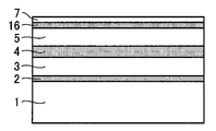
従来の分布帰還型レーザ装置としては、たとえば、図37および図38に示す装置がある(特開2000−114652号公報)。この分布帰還型レーザ装置120では、n導電型InP基板115の上に、下から順に(1)n導電型InPクラッド層116、(2)InGaAsP光閉じ込め層117,118、(3)活性層119、(4)InGaAsP光閉じ込め層120,121、(5)回折格子106、(6)p導電型InPクラッド層122、(7)p導電型InGaAsコンタクト層123が積層されている。
【0004】
図38(a)に示す分布帰還型レーザ装置における発振光であるレーザ光の装置の厚み方向に沿う光強度は、図38(b)に示すように、活性層を中心に上下に広がって分布する。図38(a)および図38(b)に示すように、回折格子高さh、すなわち波の振幅および回折格子106と活性層119との距離Hに強く依存する。
【0005】
【発明が解決しようとする課題】
しかし、回折格子高さhは、回折格子を形成する際のエッチング深さのばらつき等により大きく変動する。回折格子のエッチングは、幅0.2μm程度の微小な領域のエッチングであるため、エッチレートのウェハ面内ばらつきが大きく、また製造機会ごと、すなわちrun to runでの変動も大きい。このため、光結合係数は、回折格子高さhのばらつきの大きさに応じて変動することになる。さらに、実際には、これに加えて結晶成長における層厚ばらつきの影響も加えられる。たとえば、InGaAsP光閉じ込め層120,121が厚くなるか、またはInGaAsP光閉じ込め層118,120またはその外側の光閉じ込め層117,121が厚くなる場合、回折格子106と活性層119との距離Hが大きくなる。このため、回折格子と重なる光強度が減少し、光結合係数は小さくなる。このように、図37のような分布帰還型レーザ装置においては、製造時のわずかの膜厚変動や、組成変動に起因する屈折率変動により、光結合係数は大きくばらつき、分布帰還型レーザ装置を歩留りよく製造することは難しい。
【0006】
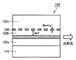
一方、上記の回折格子高さhのばらつきの影響を受けない分布帰還型レーザ装置として、たとえば、図39に示すような装置が提案されている(Journal of Lightwave Technology vol.7(1989) pp2072-2077)。この分布帰還型レーザ装置120では、InP基板115の上に、下から順に、(1)InPクラッド層122a、(2)活性層、(3)InPクラッド層122b、(4)回折格子106、(5)InPクラッド層122c、が積層されている。図39に示す分布帰還型レーザ装置の光結合係数は、2つの層厚dInP(InPクラッド層122bの厚み)およびdgrating、回折格子の屈折率および回折格子の断面形状により決定される。このため、上記回折格子が所定ピッチで桟状格子が配置される構造であれば、光結合係数は上述のエッチング深さに依存しない。したがって、図37に示した分布帰還型レーザ装置の光結合係数のばらつきの主要因である回折格子高さhに対応する要因がない。このため、図39に示す分布帰還型レーザ装置の光結合係数のばらつきは、図37に示す分布帰還型レーザ装置に比べれば小さい。
【0007】
しかしながら、層厚と屈折率とは成膜処理工程において決まるので、成膜処理装置における膜成長速度や組成の成膜処理機会ごとのばらつきや、各々の成膜処理装置固有の膜成長速度や組成の面内分布の影響を強く受ける。これらのばらつきの影響を受け、膜成長処理機会間において、またウェハ面内において光結合係数はばらつきをもつ。
【0008】
以後の説明において、成膜処理とは、(g1)下地膜と結晶方位の整合性を有するエピタキシャル膜を成長させる場合も、また(g2)結晶方位の整合性を問題にしないで結晶膜または非晶質膜を成膜する場合も含む。後者の(g2)の場合は、多結晶膜を堆積する場合等が対応する。
【0009】
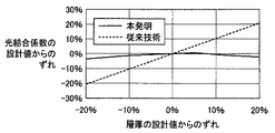
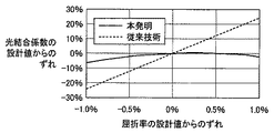
図40に、層厚dInPの変動に起因する光結合係数の設計値からのずれの計算結果を示す。また、図41に、層厚dgratingの変動に起因する光結合係数の設計値からのずれの計算結果を示す。さらに、図42に、回折格子の屈折率のばらつきに起因する光結合係数の設計値からのずれの計算結果を示す。これらの計算結果によれば、±25%の層厚変動、または±1%の屈折率変動により、光結合係数は±14〜25%も変動することが分かる。このような光結合係数のばらつきにより、分布帰還型レーザ装置の特性は大きくばらつき、その製造歩留りの向上が妨げられてきた。
【0010】
本発明は、成膜処理機会間ばらつき、成膜処理装置間ばらつきおよびウェハ面内ばらつきに起因する光結合係数の変動を抑制し、製造歩留りを向上させることができる分布帰還型レーザ装置、その分布帰還型レーザ装置とモノリシックに一体化された半導体光デバイス、および分布帰還型レーザ装置の製造方法を提供することを目的とする。
【0011】
【課題を解決するための手段】
本発明の分布帰還型レーザ装置は、半導体基板上に設けられ、活性層の両側に位置するクラッド層と、クラッド層のいずれか一方の中に、クラッド層と屈折率が異なり、光の出射方向に所定ピッチで、その出射方向に交差する方向に延びる桟状格子を有する回折格子とを備えるレーザ発振装置である。このレーザ発振装置は、回折格子と離れてクラッド層内に位置し、回折格子の組成と同じ組成を有する少なくとも一層の光分布調整層とを備える。
【0012】
この光分布調整層が回折格子を形成する前に成膜される場合には、回折格子が形成される膜と光分布調整層とは、同じ成膜処理装置中で形成される。この場合、成膜処理装置の膜形成における厚みと組成のばらつき傾向は、回折格子と光分布調整層とで同じになる。回折格子の桟状格子および光分布調整層は、屈折率がクラッド層などと比べて高い。このため、たとえば回折格子の厚さが厚く形成された場合、光分布調整層を配置しない場合、光の電界と回折格子との重なりは大きくなり、光結合係数は増大する。
【0013】
しかし、上記成膜処理装置により成膜された光分布調整層は、回折格子が形成される膜と同じ傾向でばらつくので、やはり厚くなる。光は屈折率が大きい部位に引き寄せられる性質があるため、光の電界強度分布は、上記光分布調整層が厚く形成された分だけ、光分布調整層に引き寄せられ、設計における分布よりも回折格子から遠ざけられる。この結果、光結合係数の増減がキャンセルされ、光結合係数の変動が抑制される。
【0014】
また、回折格子が形成された後に形成される光分布調整層の場合は、回折格子が形成される成膜した成膜処理装置などを用いて、やはり回折格子が形成される膜と同じばらつき傾向の光分布調整層を形成する。このため、上記と同様に、光結合係数の増減がキャンセルされ、光結合係数の変動が抑制される。
【0015】
ここで、回折格子は、通常、回折格子そのものをさす意味に用いるが、回折格子が形成されている層の意味に用いる場合もある。さらに、製造方法等の説明において回折格子膜というときには、回折格子が形成されることになる膜を意味する。
【0016】
なお、光分布調整層および回折格子の組成が同じとは、導電型を決める不純物を含めて同一の組成であってもよいし、導電型を決める不純物は互いに異なり、導電型を決める不純物以外の組成が同じであってもよい。導電型を決める不純物が異なる場合は、通常、一方はたとえばn導電型不純物を含み、他方はp導電型不純物を含む。以後の説明でも、光分布調整層および回折格子の組成が同じというとき、同様の意味とする。
【0017】
本発明の分布帰還型レーザ装置では、光分布調整層が、回折格子との間に活性層をはさむように位置することができる。
【0018】
この構成により、回折格子を形成するためのエッチング処理前に、光分布調整層と回折格子膜とを形成するので、同じ成膜処理装置内において連続して光分布調整層と回折格子膜とを成膜することができる。このため、確実に同じばらつき傾向を有する成膜処理装置により、光分布調整層と回折格子膜とを成膜するので、両方のばらつきが同じよう現れる。このため、光結合係数が増大した場合、光の電界強度分布は、光分布調整層の方にすなわち回折格子から遠ざけられるようにずれる。このような電界強度分布のずれは光結合係数の減少として作用するので、回折格子膜および光分布調整層の厚さ変動に起因する光結合係数の変動はキャンセルされる。このため、光結合係数の変動は抑制され、分布帰還型レーザ装置の特性のばらつきがなくなり、製造歩留りを向上させることができる。
【0019】
本発明の分布帰還型レーザ装置では、光分布調整層が、回折格子と活性層との間に位置することができる。
【0020】
上記構成の場合も、回折格子を形成するためのエッチング処理前に、光分布調整層と回折格子膜とを形成するので、同じ成膜処理装置内において連続して光分布調整層と回折格子膜とを成膜することができる。このため、確実に同じばらつき傾向を有する成膜処理装置により、光分布調整層と回折格子膜とを成膜するので、両方のばらつきが同じよう現れる。したがって、光結合係数の変動は抑制され、分布帰還型レーザ装置の特性のばらつきがなくなり、製造歩留りを向上させることができる。
【0021】
本発明の分布帰還型レーザ装置では、光分布調整層が、活性層との間に回折格子をはさむように位置することができる。
【0022】
この場合、活性層と回折格子とに挟まれるように位置する下側クラッド層と、回折格子と光分布調整層とに挟まれるように位置する上側クラッド層とが配置される。回折格子は、これら下側クラッド層と上側クラッド層とによって挟まれる。これら下側クラッド層と上側クラッド層とは、回折格子のエッチング処理の前後に形成されるので、同じ成膜処理装置内で連続して成膜することはできない。しかし、上記の2つのクラッド層は、同じばらつき傾向を有する成膜処理装置により形成されることができる。同じばらつき傾向を示す成膜処理装置として、たとえば(a1)同じ成膜処理装置、(a2)層厚の面内分布が類似している成膜処理装置、または(a3)同一構造の成膜処理装置を用いることができる。このような成膜処理装置を用いることにより、これら2つのクラッド層の厚みの設計値からのずれの割合の面内分布は、両方のクラッド層をほぼ同じにすることができる。
【0023】
下側クラッド層が厚くなった場合、他に何の対策もとっていなければ、活性層と回折格子との距離が大きくなるので、光結合係数は減少する。しかし、上側クラッド層も、上述のように下側クラッドと同じばらつき傾向を有する成膜処理装置により成膜されるので、その層厚が増大する。この結果、光の電界強度分布は、設計における位置よりも上側、すなわち回折格子に近づく。この電界強度分布の移動は、光結合係数の増大として作用する。この結果、両方のクラッド層の層厚変動に起因する光結合係数の変動は、キャンセルされ、光結合係数の変動は抑制される。
【0024】
本発明の分布帰還型レーザ装置では、光分布調整層が、回折格子との間に活性層をはさむように位置する第1の光分布調整層と、活性層との間に回折格子をはさむように位置する第2の光分布調整層とからなるようにできる。
【0025】
この構成により、第1の光分布調整層と回折格子膜とは、同じ成膜処理装置で連続処理のうちに成膜することができる。このため、上述の理由により、両方の厚さなど、ばらつきに起因する光結合係数の変動は互いにキャンセルして、光結合係数の変動は抑制される。
【0026】
また、回折格子の上側と下側に位置する2つのクラッド層は、たとえば上述の(a1)同じ成膜処理装置、(a2)層厚の面内分布が類似している成膜処理装置、または(a3)同一構造の成膜処理装置を用いることにより、その層厚など同じばらつき傾向とすることができる。この結果、両方のクラッド層の層厚などのばらつきに起因する光結合係数の変動は互いにキャンセルして、光結合係数の変動は抑制される。
【0027】
上記のように、光結合係数に影響を及ぼす4層が、その4層のうちで光結合係数への影響がキャンセルされる相手の層と組み合わされることにより、光結合係数の変動は抑制される。
【0028】
本発明の分布帰還型レーザ装置では、光分布調整層が、回折格子と活性層との間に位置する第3の光分布調整層と、活性層との間に回折格子をはさむように位置する第4の光分布調整層とからなるようにできる。
【0029】
この構成により、第3の光分布調整層と回折格子膜とは、同じ成膜処理装置で連続処理のうちに成膜することができる。このため、上述の理由により、両方の厚さばらつきに起因する光結合係数の変動は互いにキャンセルして、光結合係数の変動は抑制される。
【0030】
また、回折格子の上側と下側に位置する2つのクラッド層は、上述の(a1)、(a2)、または(a3)の成膜処理装置を用いることにより、その層厚など同じばらつき傾向とすることができる。この結果、両方のクラッド層の層厚などのばらつきに起因する光結合係数の変動は互いにキャンセルして、光結合係数の変動は抑制される。
【0031】
さらに、光結合係数に影響を及ぼす4層が、その4層のうちで光結合係数への影響がキャンセルされる相手の層と組み合わされることにより、光結合係数の変動は抑制される。
【0032】
本発明の分布帰還型レーザ装置では、光分布調整層の屈折率が、クラッド層の屈折率よりも高いようにできる。
【0033】
この構成により、光分布調整層が光の電界強度分布を、効果的に引き寄せることができる。
【0034】
本発明の分布帰還型レーザ装置では、回折格子が位相シフト部を有する。
【0035】
この構成により、この分布帰還型レーザ装置にさらに機能性や、レーザ発振の安定性をもたせることができる。
【0036】
本発明の分布帰還型レーザ装置では、回折格子の位相シフト部は、共振器の中央部に位置して媒質内波長の1/4に相当する位相をシフトさせることができる。
【0037】
この構成により、共振器の両端面に無反射コーティングを施すことにより、単一縦モードの歩留りを向上させることができる。
【0038】
本発明の分布帰還型レーザ装置では、半導体基板が不純物を含むInP基板であり、活性層がInGaAsP層であり、クラッド層が不純物を含むInP層であり、回折格子および光分布調整層が不純物を含むInGaAsP層であるようにできる。
【0039】
この構成により、従来の製造装置を用いて、InP/InGaAsP系の分布帰還型レーザ装置を歩留りよく製造することができる。
【0040】
本発明の半導体光装置は、上記のいずれかの分布帰還型レーザ装置と、他の光デバイスとを共通の半導体基板上にモノリシックに備える。
【0041】
この構成により、分布帰還型レーザ装置と、他の光デバイスとがモノリシックに一体化されているので、装置が小型化される。また、一連の処理工程で2つの装置を一体化して製造できるので、製造能率を大きく向上することができる。
【0042】
本発明の半導体光装置は、他の光デバイスが変調器であり、その変調器が分布帰還型レーザ装置の活性層から光を受ける吸収層を備えることができる。
【0043】
このモノリシックに一体化した装置では、電極間に電圧を印加し、活性層に電流を注入し、活性層の層に沿って発振させるとともに、回折格子などにより特定の波長選択がなされ特定波長の発振が継続する。発振した光は、活性層から変調器の吸収層に導波され、変調器の電極間に印加される電圧により変調をかけることができる。この分布帰還型レーザ装置には、上記のいずれかの分布帰還型レーザ装置が用いられるので、製造時のばらつきに起因する光結合係数の変動が大幅に抑制される。さらに、分布帰還型レーザ装置と変調器とがモノリシックに一体化されているので、装置が小型化される。また、一連の処理工程で2つの装置を一体化して製造できるので、製造能率を大きく向上することができる。
【0044】
本発明の分布帰還型レーザー装置の製造方法は、半導体基板上に設けた活性層の両側に位置するクラッド層と、クラッド層のいずれか一方の中に、クラッド層と屈折率が異なり、光の出射方向に所定ピッチで、その出射方向に交差する方向に延びる桟状格子が配置された回折格子と、回折格子と離れてクラッド層内に位置し、回折格子の組成と同じ組成を有する少なくとも一層の光分布調整層と、を有する分布帰還型レーザー装置の製造方法である。この製造方法では、少なくとも一層の光分布調整層の成膜処理と、回折格子を形成する膜の成膜処理とを、(a1)同じ成膜処理装置、(a2)層厚の面内分布が類似している成膜処理装置、および(a3)同一構造の成膜処理装置、のいずれかを用いて行う。
【0045】
この製造方法により、光分布調整層のばらつき傾向と、回折格子膜のばらつき傾向とを同じようにすることができる。このため、これら両方の製造時のばらつきに起因する光結合係数に及ぼす変動要因を、互いに相反させ、したがってキャンセルするようにすることができる。この結果、製造時のばらつきに起因する光結合係数の変動を抑制することができ、歩留りを向上させることができる。
【0046】
本発明の分布帰還型レーザー装置の製造方法では、光分布調整層が、回折格子を形成する膜をエッチング処理するために、回折格子を形成する膜を形成した成膜処理装置から取り出され、エッチング処理された後、成膜処理装置内で成膜されることができる。
【0047】
この構成により、エッチング処理のためにエッチング処理装置に装入され、そのエッチングの前後になされる成膜処理であっても、上記のように成膜処理装置を選ぶことにより、2つの成膜処理におけるばらつき傾向を同じようにすることができる。
【0048】
本発明の分布帰還型レーザー装置の製造方法では、回折格子および回折格子を含むクラッド層の形成において、回折格子の下層に相当する位置に下側クラッド層を形成し、下側クラッド層の上に、回折格子が形成される回折格子膜を形成し、その回折格子膜をエッチング処理して桟状格子を含む回折格子を形成し、さらにその回折格子の上に前記エッチングされた部分を埋め込むように上側クラッド層を形成するにあたり、下側クラッド層の成膜処理と、上側クラッド層の成膜処理とを、(a1)同じ成膜処理装置、(a2)層厚の面内分布が類似している成膜処理装置、および(a3)同一構造の成膜処理装置、のいずれかを用いて行うことができる。
【0049】
この構成により、回折格子を上下からはさむ上側クラッド層と下側クラッド層とを、同じばらつき傾向をもつように成膜することができる。このため、回折格子膜と光分布調整層との同じばらつき傾向に基づく光結合係数の変動抑制に加えて、これら両クラッド層の製造時のばらつきに起因する光結合係数に及ぼす変動要因を、互いにキャンセルするようにすることができる。この結果、製造時のばらつきに起因する光結合係数の変動を抑制することができ、歩留りを向上させることができる。
【0050】
【発明の実施の形態】
次に図面を用いて本発明の実施の形態について説明する。
【0051】
(実施の形態1)
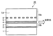
図1は、本発明の実施の形態1における分布帰還型レーザ装置を示す図である。図1において、n導電型InP基板1の上に、n導電型InGaAsP層2が位置し、さらにその上に、n導電型InP層3が設けられている。その上に活性層4を構成するInGaAsP層が位置し、その活性層4の上に、p導電型InP層5が設けられ、さらにその上にn導電型InGaAsP層からなる桟状格子が所定ピッチで配置された回折格子6が位置する。この桟状格子の間の溝を埋め込むように、p導電型InP層7,8が設けられている。
【0052】
InP層からなるクラッド層18a,18bは、活性層4を上下から挟んでいる。また、上記のn導電型InGaAsP層2が光分布調整層を構成する。図1に示すように、クラッド層18bは、n導電型InP基板1に接して位置する光分布調整層の上に接して配置されている。このように半導体基板1上に接して位置する光分布調整層の上に接してクラッド層が位置する場合も、半導体基板およびクラッド層の組成は同じであるので、光分布調整層はクラッド層内に位置するという。すなわち、光分布調整層がクラッド層(InP)と半導体基板(InP)とに挟まれる場合、光分布調整層は実質的にクラッド層内に配置されているとみることができる。
【0053】
また、以後の説明では、回折格子と、回折格子が形成されることになる回折格子膜とは、図面中で同じ符号によって表わされる。
【0054】
この分布帰還型レーザ装置では、活性層4に電流を注入し、活性層の層に沿って発振させるとともに、回折格子6の桟状格子ピッチなどにより特定の波長選択がなされ特定波長の発振が継続する。図1に示すように、発振中の光のうちから光を部分的に外部に取り出し、光ファイバ通信等に用いる。
【0055】
次に、上記分布帰還型レーザ装置の製造方法について説明する。図2に示すように、n導電型InP基板1の上に、下から順に、(1)光分布調整層となるn導電型InGaAsP層2、(2)n導電型InP層3、(3)InGaAsP層からなる活性層4、(4)p導電型InP層5、(5)回折格子が形成されるn導電型InGaAsP膜6、(6)p導電型InP層7、が形成される。
【0056】
これらの成膜処理において重要なことは、少なくとも、光分布調整層となるn導電型InGaAsP層2と、回折格子が形成されるn導電型InGaAsP膜6とは、同じばらつき傾向を持つ処理装置内で、そのばらつき傾向が変わらない処理機会、たとえば同一処理機会に形成されなければならない。すなわち、たとえばInPウェハを一枚ずつバッチ処理する場合には、そのInPウェハ上に、同じ成膜処理装置内で連続して、光分布調整層となるn導電型InGaAsP層2と、回折格子が形成されるn導電型InGaAsP膜6とを成膜する必要がある。ここで、ばらつき傾向が同じとは、ばらつく方向が同じで、かつそのばらつきの大きさが同じ程度であることをさす。また、面内ばらつきを問題にする場合には、ばらつきの方向も含めてばらつきの面内分布が類似していることをいう。
【0057】
上記の成膜処理方法としては、MOCVD法(Metal Organic Chemical Vapor Deposition:有機金属気相成長法 )、MBE法(Molecular Beam Epitaxy)、LPE法(Liquid Phase Epitaxy)を用いることができる。
【0058】
この後、図3に示すように、干渉露光法、電子ビーム露光法およびエッチングとにより、n導電型InGaAsP膜6と、p導電型InP層7とを所定ピッチの桟状格子となるように、パターニングする。この上に、上記ピッチ間の溝を埋め込むように、p導電型InP層8を成膜して分布帰還形レーザ装置が完成する。
【0059】
上記図1の分布帰還型レーザ装置の構成において、光分布調整層のn導電型InGaAsP層2は、回折格子の桟状格子を構成するn導電型InGaAsP層6と、導電型を決める不純物を含めて同じ組成である。上述したように、上記の2つの層は同じ処理機会に同じ処理装置内で相前後して形成されるために、両層の厚さおよび組成は同じばらつき傾向を示す。したがって、両層が屈折率の設計値からずれる割合は、両層ともほとんど同じである。たとえば、回折格子が形成されるInGaAsP層6が厚くなった場合、従来の分布帰還型レーザ発振装置では、回折格子と発振電界分布との重なりが増大して光結合係数は増大する。しかし、本実施の形態では、光分布調整層であるInGaAsP層2も、回折格子が形成されるInGaAsP膜6と同様の傾向で、設計厚に対して同じような割合で厚くなる。
【0060】
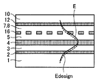
光は屈折率の高い領域に引き付けられるので、光分布調整層の厚みがばらついて厚くなった分だけ、光の電界強度分布は、設計における発振位置から光分布調整層の方に引き寄せられる。図4は、上記の光分布調整層であるInGaAsP層2が厚くなったことにより、導波路厚さ方向に沿った断面での光の電界強度分布がInGaAsP層2の側に引き寄せられたことを示す図である。破線は設計における電界強度分布Edesignを表し、実線が光分布調整層がばらついて厚くなった後の電界強度分布Eを示している。上記のような光電界強度分布のずれは、光結合係数を減少させる方向に作用する。この結果、光分布調整層における回折格子膜と同じ傾向の厚み変動は、回折格子における厚み変動に起因する光結合係数の変動を補償することができる。
【0061】
また、回折格子が形成されるInGaAsP膜6が薄くなった場合には、光分布調整層であるInGaAsP層2も、同じ傾向でばらつき、薄くなる。このとき、上記図4の場合と同じメカニズムが作用して光結合係数の変動を補償する。すなわち、図5に示すように、分布調整層が薄くなった分、導波路厚さ方向に沿う光の電界強度分布は、EdesignからEへと引き寄せられる。すなわち、設計における光電界強度分布よりも光分布調整層から斥けられ、回折格子側に引き寄せられる。
【0062】
上記は厚み変動に対してのみ説明したが、回折格子の桟状格子を構成するInGaAsP層6の組成変動に起因する屈折率変動が生じた場合でも、光分布調整層2がその変動を補償し、その結果、光結合係数の変動を補償する。
【0063】
上記のように、回折格子を形成する層において、組成変動や厚み変動があっても、これら変動に起因する光結合係数の変動を抑制することができる。これをまとめると次のように要約される。
(1)回折格子と同じ組成の光分布調整層を、回折格子との間に活性層をはさむように配置する。
(2)この光分布調整層の配置を含めて、分布帰還型レーザ装置を設計する。
(3)分布帰還型レーザ装置製造の際に、回折格子膜に、厚み変動や組成変動が生じる場合、光分布調整層も同じ傾向の厚み変動や組成変動が生じる。回折格子膜と、光分布調整層とで同じ傾向の厚み変動や組成変動が生じるためには、両層が同じばらつき傾向を示す成膜処理装置内で形成されるようにする。たとえば、同一バッチ処理において同じ成膜処理装置内で連続して形成されることが望ましい。回折格子膜のエッチング処理をはさんで、回折格子膜の成膜処理と、光分布調整層の成膜処理とが行われる場合には、回折格子膜の成膜処理と、光分布調整層の成膜処理とを、同じ成膜処理装置内で連続して行うことはできない。しかし、同じ成膜処理装置を用いたり、少なくとも同じようなばらつき傾向を示す成膜処理装置内で成膜することが望ましい。
(4)回折格子の厚み変動および組成変動に起因する光結合係数の変動と、光分布調整層の厚み変動および組成変動に起因する光結合係数の変動とがキャンセルして、光結合係数の変動が抑制される。この結果、分布帰還型レーザ装置の特性ばらつきを抑制することができ、歩留りの向上が得られる。
【0064】
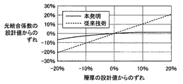
図6に、本発明の分布帰還型レーザ装置の回折格子に厚み変動が生じた場合の光結合係数の設計値からのずれの計算結果を示す。また、図7に、本発明の分布帰還型レーザ装置の回折格子に組成変動が生じ、そのために屈折率変動が生じた場合の光結合係数の設計値からのずれの計算結果を示す。図6および図7によれば、本発明の分布帰還型レーザ装置では、光結合係数の変動は従来に比較しておよそ1/8に抑制されている。この結果、分布帰還型レーザ装置の特性ばらつきを抑制することができる。
【0065】
なお、本実施の形態では、活性層の上側に回折格子が配置されるものとして説明したが、回折格子は活性層の下側にあってもよい。各半導体のn導電型とp導電型とを逆にしてもよい。また、回折格子の一部に回折格子の位相がシフトしている個所が1箇所または複数箇所あってもよい。回折格子の共振器の中央部分に媒質内波長の1/4に相当する位相シフトを設け、両端面に無反射コーティングを施すこともできる。この位相シフトと無反射コーティングとにより、単一縦モード歩留りを向上させることができる。
【0066】
本実施の形態では、InP/InGaAsP系の分布帰還型レーザ装置について説明した。しかし、たとえば、InP/AlGaInAs系の分布帰還型レーザ装置(第62回応用物理学会学術講演会(2001年)13p-B-15)などに適用することもできる。さらに、本実施の形態は、たとえば、変調器と分布帰還型レーザ装置とを共通基板上にモノリシックに集積化した装置(IEEE Journal of Quantum Electronics, vol.36(2000)pp909-915)における分布帰還型レーザ装置に適用することもできる。
【0067】
(実施の形態2)
図8は、本発明の実施の形態2における分布帰還型レーザ装置の構成を示す図である。本実施の形態では、光分布調整層12が回折格子16と活性層4との間に配置されている点に特徴がある。図8において、光分布調整層12と回折格子16とは、クラッド層18a内に配置されている。
【0068】
図8において、n導電型InP基板1の上に、n導電型InP層3が位置し、その上に活性層を構成するInGaAsP層4が設けられ、さらにその上にp導電型InP層5が位置する。そのp導電型InP層5の上に、光分布調整層のp導電型InGaAsP層12が位置し、その上にp導電型InP層7が設けられる。さらに、回折格子の桟状格子を構成するp導電型InGaAsP層16が配置されている。このp導電型InGaAsP層16を覆うように、p導電型InP層8,9が配置されている。回折格子の桟状格子を形成するp導電型InGaAsP層16と、光分布調整層のp導電型InGaAsP層12とは、導電型を決める不純物を含めて同じ組成である。
【0069】
この分布帰還型レーザ装置では、活性層4に電流を注入し、活性層に沿うように発振させるとともに、回折格子16の所定ピッチの桟状格子により特定の波長選択がなされ特定波長の発振が継続する。図8に示すように、発振中の光から部分的に外部に光を取り出し、光ファイバ通信等に用いる。
【0070】
次に、上記分布帰還型レーザ装置の製造方法について説明する。図9に示すように、n導電型InP基板1の上に、下から順に、(1)n導電型InP層3、(2)InGaAsP層からなる活性層4、(3)p導電型InP層5、(4)光布調整層となるp導電型InGaAsP層12、(5)p導電型InP層7、(6)回折格子が形成されるp導電型InGaAsP膜16、(7)p導電型InP層8、が形成される。
【0071】
これらの成膜処理において重要なことは、少なくとも、光分布調整層となるp導電型InGaAsP層12と、回折格子が形成されるp導電型InGaAsP膜16とは、同じばらつき傾向を持つ処理装置内で、そのばらつき傾向が変わらない処理機会、たとえば同一処理機会に形成されなければならない。すなわち、たとえばInPウェハを一枚ずつバッチ処理する場合には、そのInPウェハ上に、同じ成膜処理装置内で連続して、光分布調整層となるn導電型InGaAsP層2と、回折格子が形成されるn導電型InGaAsP膜16とを成膜する必要がある。ここで、ばらつき傾向が同じとは、ばらつく方向が同じで、かつそのばらつきの大きさが同じ程度であることをさす。また、面内ばらつきを問題にする場合には、ばらつきの方向も含めてばらつきの面内分布が類似していることをいう。
【0072】
上記の成膜処理方法としては、MOCVD法(Metal Organic Chemical Vapor Deposition:有機金属気相成長法 )、MBE法(Molecular Beam Epitaxy)、LPE法(Liquid Phase Epitaxy)を用いることができる。
【0073】
この後、図10に示すように、干渉露光法、電子ビーム露光法およびエッチングとにより、p導電型InGaAsP層16と、p導電型InP層8とを所定ピッチの桟状格子となるように、パターニングする。この上に、上記ピッチ間の溝を埋め込むように、p導電型InP層9を成膜して分布帰還形レーザ装置が完成する。
【0074】
図8の分布帰還型レーザ装置の構成において、光分布調整層InGaAsP12は、回折格子の桟状格子を構成するInGaAsP層16と同じ組成である。上記の2つの層は同じ処理機会に同じ処理装置内で連続して形成する。このために、両層の厚みおよび組成は同じばらつき傾向を示す。したがって、両層が屈折率の設計値からずれる割合は、両層ともほとんどである。たとえば、回折格子を構成するInGaAsP層16が厚くなった場合、従来の分布帰還型レーザ発振装置では光結合係数は増大する。しかし、本実施の形態では、光分布調整層であるInGaAsP層12も、回折格子の桟状格子を構成するInGaAsP層16と同様の傾向で同じ割合で厚くなる。
【0075】
上述のように、光は屈折率の高い領域に引き付けられるので、図11に示すように、光の電界強度分布は、回折格子16から遠ざけられ、p導電型InGaAsP層12のほうに引き寄せられる。このような光電界強度分布のずれは、光結合係数を減少させる方向に作用する。この結果、InGaAsP層16の層の厚み変動に起因する光結合係数のずれを抑制することができる。
【0076】
一方、回折格子が形成されるp導電型InGaAsP膜16が薄くなった場合には、光分布調整層であるp導電型InGaAsP層12も薄くなるようにばらつく。この結果、図12に示すように、導波路厚さ方向に沿う電界強度分布は回折格子側に引き寄せられる。図12の場合も、上記図4の場合と厚み変動に対して同じメカニズムが作用して光結合係数の変動を補償することができる。
【0077】
上記は厚み変動に対してのみ説明したが、回折格子の桟状格子を構成するInGaAsP層16の組成変動に起因する屈折率変動が生じた場合でも、光分布調整層12がその変動を補償し、その結果、光結合係数の変動を補償する。
【0078】
上記のように、回折格子を形成する層において、組成変動や厚み変動があっても、これら変動に起因する光結合係数の変動を抑制することができる。
【0079】
なお、本実施の形態では、活性層の上側に回折格子が配置されるものとして説明したが、回折格子は活性層の下側にあってもよい。半導体の導電型のn導電型とp導電型とを入れ換えてもよい。また、回折格子の一部に回折格子の位相がシフトしている個所が1箇所または複数箇所あってもよい。回折格子の共振器の中央部分に媒質内波長の1/4に相当する位相シフトを設け、両端面に無反射コーティングを施すこともできる。この位相シフトと無反射コーティングとにより、単一縦モード歩留りを向上させることができる。
【0080】
本実施の形態では、InP/InGaAsP系の分布帰還型レーザ装置について説明した。しかし、たとえば、InP/AlGaInAs系の分布帰還型レーザ装置などに適用することもできる。さらに、本実施の形態は、たとえば、変調器と分布帰還型レーザ装置とを共通基板上にモノリシックに集積化した装置における分布帰還型レーザ装置に適用することもできる。
【0081】
(実施の形態3)
図13は、本発明の実施の形態3における分布帰還型レーザ装置の構成を示す図である。本実施の形態では、光分布調整層12が、活性層4との間に回折格子16をはさむ位置に設けられている点に特徴がある。図13において、n導電型InP基板1の上に、n導電型InP層3が位置し、さらにその上に活性層4を構成するInGaAsP層が設けられている。活性層4の上に、p導電型InP層5が位置し、その上にp導電型InGaAsP膜から形成された回折格子16が位置する。その上に回折格子の桟状格子の間のエッチング溝を埋め込むように、p導電型InP層7が設けられ、その上に光分布調整層であるp導電型InGaAsP層12が位置する。このp導電型InGaAsP層12の上にはp導電型InP層9が設けられている。光分布調整層12はクラッド層18a内に配置されている。
【0082】
次に、上記分布帰還型レーザ装置の製造方法について説明する。まず、図14に示すように、n導電型InP基板1の上に、下から順に、(1)n導電型InP層3、(2)InGaAsP層からなる活性層4、(3)p導電型InP層5、(4)回折格子が形成されるp導電型InGaAsP膜16、(5)p導電型InP層7を形成する。
【0083】
この後、図15に示すように、干渉露光法、電子ビーム露光法およびエッチングとにより、p導電型InGaAsP膜16と、p導電型InP層7とをパターニングして、回折格子の桟状格子を形成する。この上に、回折格子のエッチング溝を埋め込むようにp導電型InP層8を形成し、さらにその上にp導電型InP層9を成膜して、図13に示す分布帰還型レーザ装置が完成する。
【0084】
重要なことは、少なくとも、活性層4と回折格子16とにはさまれるp導電型InP層5と、回折格子16と光分布調整層12とにはさまれるp導電型InP層7,8は、同じばらつき傾向を有する成膜処理装置により形成される必要がある。同じばらつき傾向を示す成膜処理装置として、(a1)同じ成膜処理装置、(a2)層厚の面内分布が類似している成膜処理装置、または(a3)同一構造の成膜処理装置を用いることができる。このような成膜処理装置を用いることにより、これらInP層の厚みの設計値からのずれの割合の面内分布は、両方のp導電型InP層でほぼ同じにすることができる。
【0085】
上記の成膜処理方法としては、MOCVD法(Metal Organic Chemical Vapor Deposition:有機金属気相成長法 )、MBE法(Molecular Beam Epitaxy)、LPE法(Liquid Phase Epitaxy)を用いることができる。
【0086】
たとえば、p導電型InP層5が厚くなった場合、活性層と回折格子との距離が増大するので、従来の装置では光結合係数は減少する。しかし、本実施の形態では、p導電型InP層7,8も、p導電型InP層5と同じ割合で厚くなる。このため、p導電型InP層7,8の厚み増大の効果により、図16に示すように、導波路厚み方向に沿う電界強度分布Eは、Edesignからずれて、回折格子の側に引き寄せられる。この電界強度分布の回折格子の側への引き寄せは、光結合係数を増加させるので、p導電型InP層5の厚み増加に伴う光結合係数の減少を補償することができる。
【0087】
一方、p導電型InP層5が薄くなった場合、活性層と回折格子との距離が減少するので、従来の装置では光結合係数は増大する。しかし、本実施の形態では、p導電型InP層7,8も、p導電型InP層5と同じ傾向で薄くなる。このため、図17に示すように、導波路厚み方向に沿う電界強度分布は、Edesignからずれて、活性層4の側、すなわち回折格子から遠い側へと移動させられる。したがって、この場合にも光結合係数の変動を補償することができる。
【0088】
図18に、本発明の分布帰還型レーザ装置において、InP層に厚み変動が生じた場合の光結合係数の設計値からのずれの計算結果を示す。図18によれば、本発明の分布帰還型レーザ装置では、光結合係数の変動は従来に比較しておよそ1/6に抑制されている。この結果、分布帰還型レーザ装置の特性ばらつきを抑制することができる。
【0089】
なお、本実施の形態では、活性層の上側に回折格子が配置されるとして説明したが、回折格子は活性層の下側にあってもよい。また、半導体の導電型のn導電型とp導電型とを入れ換えてもよい。また、回折格子の一部に回折格子の位相をシフトさせる個所が1箇所または複数箇所あってもよい。回折格子の共振器の中央部分に媒質内波長の1/4に相当する位相シフトを設け、両端面に無反射コーティングを施すこともできる。この位相シフトと無反射コーティングとの組合せにより、単一縦モード歩留りを向上させることができる。
【0090】
このほか、たとえば、InP/AlGaInAs系の分布帰還型レーザ装置などに適用することもできる。さらに、本発明は、たとえば、変調器と分布帰還型レーザ装置とを共通基板上にモノリシックに集積化した装置における分布帰還型レーザ装置に適用することもできる。
【0091】
(実施の形態4)
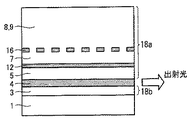
図19は、本発明の実施の形態4における分布帰還型レーザ装置を示す図である。本実施の形態では、分布帰還型レーザ装置に2つの光分布調整層2,12を設けた点に特徴がある。すなわち、実施の形態1の分布帰還型レーザ装置における光分布調整層2と、実施の形態3の分布帰還型レーザ装置における光分布調整層12とを備えている。光分布調整層2はInP層のクラッド層18b内に配置され、またはより具体的にはクラッド層18bとInP基板1との間に配置され、光分布調整層12はクラッド層18a内に配置されている。
【0092】
図19において、n導電型InP基板1の上に、第1の光分布調整層となるn導電型InGaAsP層2が位置し、その上にn導電型InP層3が設けられている。さらにその上に活性層のInGaAsP層4が位置し、その活性層の上にp導電型InP層5が設けられている。その上にn導電型InGaAsP層2と同じバンドギャップを有するn導電型InGaAsP層から形成された回折格子16が位置し、その上に回折格子の桟状格子の間の溝を埋め込むように、p導電型InP層7,8が設けられている。このp導電型InP層7,8の上には、第2の光分布調整層となるp導電型InGaAsP層12が位置し、その上にp導電型InP層10が設けられている。
【0093】
次に、図19に示す分布帰還型レーザ装置の製造方法について説明する。まず、図20に示すように、n導電型InP基板1の上に、下から順に、(1)n導電型InGaAsP層2、(2)n導電型InP層3、(3)InGaAsP活性層4、(4)p導電型InP層5、(5)n導電型InGaAsP層2と同一のバンドギャップを有するp導電型InGaAsP膜16、(6)p導電型InP層7を、同じ成膜処理において成膜する。この成長処理には、MOCVD法、MBE法、LPE法などを用いることができる。
【0094】
その後、干渉露光法や電子ビーム露光法と、エッチングにより、p導電型InGaAsP層16およびp導電型InP層7を、図21に示すように、所定のピッチで除去することにより所定ピッチの桟状格子を分布させることにより回折格子を形成する。この後、(7)p導電型InP層8を回折格子の桟状格子間の溝を埋め込むように形成し、さらに(8)p導電型InGaAsP層12を成膜し、この上に(9)p導電型InP層10を形成する。
【0095】
上記の成膜処理において、回折格子を形成するためのエッチング処理をはさんで、エッチング処理より前の第1の成膜処理と、エッチングより後の第2の成膜処理とは、(a1)同じ成膜処理装置、(a2)層厚の面内分布が類似している成膜処理装置、または(a3)同一構造の成膜処理装置を用いる。
【0096】
第1の光分布調整層であるn導電型InGaAsP層2と、回折格子が形成されるn導電型InGaAsP膜16とは、いずれも上記エッチング前に成膜処理される。このため、これら2つのn導電型InGaAsP層は、同一組成であり、また連続した成膜処理によって形成される。このため、層厚および組成、または屈折率の設計値からずれる割合は、これら2つのn導電型InGaAsP層において、ほぼ同じである。
【0097】
n導電型InGaAsP膜16が厚く形成された場合、従来の分布帰還レーザ装置では、光結合係数は増大する。しかし、本実施の形態では、n導電型InGaAsP層2も同じ割合で厚くなるため、導波路厚み方向に沿う電界強度分布は、設計における電界強度分布Edesignよりもn導電型InGaAsP層2の方に、すなわち回折格子から遠ざかる方向に引き寄せられる(図22)。このような電界強度分布のずれは、光結合係数を減少させる方向に作用するため、上記2つのn導電型InGaAsP層の厚みを適切に選ぶことにより、これら2つの厚み変動に起因する光結合係数の変動を抑制することができる。
【0098】
一方、n導電型InGaAsP膜16が薄く形成された場合、光結合係数は小さくなる。しかし、このときn導電型InGaAsP層2も、上記理由に基づき薄く形成される。このため、導波路厚さ方向に沿う電界強度分布は、回折格子の側に引き寄せられる(図23)。この電界強度分布の移動により、光結合係数は増大する。したがって、この場合も上記2つのn導電型InGaAsP層の厚みを適切に選ぶことにより、これら2つの層の厚み変動に起因する光結合係数の変動を補償することができる。
【0099】
また、回折格子をはさむp導電型InP層5とp導電型InP層7,8とは、上述のように(a1),(a2),(a3)の成膜処理装置によって成膜されるので、同様の層厚の面内分布となる。このため、これら2つの層の設計値に対してずれる割合の面内分布は、これら2つの層でほぼ同様である。
【0100】
したがって、p導電型InP層5が設計値より厚くなった場合、従来技術では光結合係数は減少する。しかし、本実施の形態では、p導電型InP層7,8も同じ割合で厚くなるので、導波路厚さ方向に沿う光電界強度分布Eは、設計における電界強度分布Edesignよりも回折格子側に引き寄せられる(図24)。この電界強度分布のずれは、光結合係数を増加させる方向に作用させ、2つの層の厚さの同じ傾向の変動に起因する光結合係数の変動は互いにキャンセルされる。この結果、製造時の層厚のばらつきに起因する光結合係数の変動は抑制される。
【0101】
一方、p導電型InP層5が設計値より薄くなった場合、従来技術では光結合係数は増大する。しかし、本実施の形態では、p導電型InP層7,8も同じ割合で薄くなるので、導波路厚さ方向に沿う光電界強度分布Eは、設計における電界強度分布Edesignよりも回折格子側から遠ざけられる(図25)。この電界強度分布のずれは、光結合係数を増加させる方向に作用させ、2つの層の厚さの同じ傾向の変動に起因する光結合係数の変動は互いにキャンセルされる。この結果、光結合係数は製造時の層厚のばらつきで大きく変動することがなくなる。
【0102】
上記のように、本実施の形態における分布帰還型レーザ装置の構成により、回折格子が形成される層の組成や厚み変動に起因する光結合係数の変動を抑制することができる。さらに、回折格子を挟んで位置するp導電型InP層の厚み変動に起因する光結合係数の変動も、両方のp導電型InP層の同傾向の厚み変動が光結合係数に対して相反する方向の作用を及ぼすので、光結合係数の変動の抑制が得られる。
【0103】
本実施の形態における光結合係数の変動抑制を定量的に計算で評価した結果を、図26〜図28に示す。図26は、p導電型InP層の厚みが変動した場合の光結合係数の設計値からのずれを示している。この図によれば、従来の装置に比較して、本実施の形態では、光結合係数はほとんど(1/2)に減少している。図27は、回折格子の厚みが変動した場合の光結合係数の設計値からのずれを示している。この図によれば、従来の装置に比較して本実施の形態の装置では、(1/2)以下に減少している。また、図28は、回折格子の屈折率が変動した場合の光結合係数の設計値からのずれを示している。この図によれば、従来の装置に比較して本実施の形態の装置では、(1/2)よりも大幅に減少している。
【0104】
本実施の形態においても、実施の形態1〜3と同様に、活性層の下方に回折格子を配置した分布帰還型レーザ装置であってもよい。また、半導体のn導電型とp導電型とを入れ換えてもよい。また、位相シフトが設けられた回折格子を有する分布帰還型レーザ装置であってもよい。また、他の材料系、たとえばInP/AlGaInAs系の分布帰還型レーザ装置であってもよい。さらに、変調器を集積化した分布帰還型レーザ装置であってもよい。
【0105】
(実施の形態5)
図29は、本発明の実施の形態5における分布帰還型レーザ装置を示す図である。本実施の形態では、実施の形態4と同様に、分布帰還型レーザ装置に2つの光分布調整層12a,12bを設けた点に特徴がある。すなわち、実施の形態2の分布帰還型レーザ装置における光分布調整層12aと、実施の形態3の分布帰還型レーザ装置における光分布調整層12bとを備えている。2つの光分布調整層12a,12bは、ともにクラッド層18a内に配置されている。
【0106】
図29において、n導電型InP基板1の上に、n導電型InP層3が位置し、その上に活性層のInGaAsP層4が設けられている。活性層の上にはp導電型InP層5が位置し、その上に第1の光分布調整層となるp導電型InGaAsP層12aが位置し、その上にp導電型InP層7が設けられている。そのp導電型InP層7の上には、回折格子16が位置し、次いでp導電型InP層8,9、および第2の光分布調整層となるp導電型InGaAsP層12bが位置し、その上にp導電型InP層10が設けられている。
【0107】
次に、図29に示す分布帰還型レーザ装置の製造方法について説明する。まず、図30に示すように、n導電型InP基板1の上に、下から順に、(1)n導電型InP層3、(2)InGaAsP活性層4、(3)p導電型InP層5、(4)p導電型InGaAsP層12a、(5)p導電型InP層7、(6)p導電型InGaAsP膜16、(7)p導電型InP層8、を同じ成膜処理装置において成膜する。この成長処理には、MOCVD法、MBE法、LPE法などを用いることができる。
【0108】
その後、干渉露光法や電子ビーム露光法と、エッチングとにより、p導電型InGaAsP膜16およびp導電型InP層8を、図31に示すように、パターニングして、桟状格子を形成する。この後、(8)p導電型InP層9を回折格子の桟状格子の間の溝を埋め込むように形成し、さらに(9)p導電型InGaAsP層12bを、次いで、この上に(10)p導電型InP層10を形成する。
【0109】
上記の成膜処理において、回折格子を形成するためのエッチング処理をはさんで、エッチング処理より前の第1の成膜処理と、エッチングより後の第2の成膜処理とは、(a1)同じ成膜処理装置、(a2)層厚の面内分布が類似している成膜処理装置、または(a3)同一構造の成膜処理装置を用いて行う。
【0110】
第1の光分布調整層であるp導電型InGaAsP層12aと、回折格子が形成されるp導電型InGaAsP膜16とは、いずれも上記エッチング前に成膜処理される。このため、これら2つのp導電型InGaAsP層は、また連続した成膜処理によって形成される。このため、層厚および組成、または屈折率の設計値からずれる割合は、これら2つのp導電型InGaAsP層において、ほぼ同じである。
【0111】
p導電型InGaAsP膜16が厚く形成された場合、従来の分布帰還レーザ装置では、光結合係数は増大する。しかし、本実施の形態では、p導電型InGaAsP層12aも、同じ割合で厚くなるため、導波路厚み方向に沿う電界強度分布Eは、設計における電界強度分布Edesignよりもp導電型InGaAsP層12aの側に、すなわち回折格子から遠ざかる方向に押される(図32)。このような電界強度分布のずれは、光結合係数を減少させる方向に作用するため、上記2つのp導電型InGaAsP膜の厚みを適切に選ぶことにより、これら2つの層の厚み変動に起因する光結合係数の変動を補償することができる。
【0112】
一方、p導電型InGaAsP膜16が薄く形成された場合、光結合係数は小さくなる。しかし、このときp導電型InGaAsP層12aも、上記理由に基づき薄く形成される。このため、導波路厚さ方向に沿う電界強度分布は、回折格子の側に引き寄せられる(図33)。この引き寄せにより、光結合係数は増大する。したがって、この場合も上記2つのp導電型InGaAsP層の厚みを適切に選ぶことにより、これら2つの層の厚み変動に起因する光結合係数の変動を補償することができる。
【0113】
また、回折格子をはさむp導電型InP層7とp導電型InP層8,9とは、上述のように(a1),(a2),(a3)の成膜処理装置によって成膜されるので、同様の層厚の面内分布となる。このため、これら2つの層の設計値に対してずれる割合の面内分布は、これら2つの層でほぼ同様である。
【0114】
したがって、p導電型InP層7が設計値より厚くなった場合、従来技術では光結合係数は減少する。しかし、本実施の形態では、p導電型InP層8,9も同じ割合で厚くなるので、導波路厚さ方向に沿う光電界強度分布Eは、設計における電界強度分布Edesignよりも回折格子側に引き寄せられる(図34)。この電界強度分布のずれは、光結合係数を増加させる方向に作用させ、2つの層の厚さの同じ傾向の変動に起因する光結合係数の変動は互いにキャンセルされる。この結果、光結合係数は製造時の層厚のばらつきで大きく変動することがなくなる。
【0115】
一方、p導電型InP層7が設計値より薄くなった場合、従来技術では光結合係数は増大する。しかし、本実施の形態では、p導電型InP層8,9も同じ割合で薄くなるので、導波路厚さ方向に沿う光電界強度分布Eは、設計における電界強度分布Edesignよりも回折格子側から遠ざけられる(図35)。この電界強度分布のずれは、光結合係数を増加させる方向に作用させ、2つの層の厚さの同じ傾向の変動に起因する光結合係数の変動は互いにキャンセルされる。この結果、光結合係数は製造時の層厚のばらつきで大きく変動することがなくなる。
【0116】
上記のように、本実施の形態における分布帰還型レーザ装置の構成により、回折格子が形成される層の組成や厚み変動に起因する光結合係数の変動を抑制することができる。さらに、回折格子を挟んで位置するp導電型InP層の厚み変動に起因する光結合係数の変動も、両方のp導電型InP層の同傾向の厚み変動が光結合係数に対して相反する方向の作用を及ぼすので、光結合係数の変動の抑制が得られる。
【0117】
本実施の形態においても、実施の形態1〜4と同様に、活性層の下方に回折格子を配置した分布帰還型レーザ装置であってもよいし、位相シフトが設けられた回折格子を有する分布帰還型レーザ装置であってもよい。また、他の材料系、たとえばInP/AlGaInAs系の分布帰還型レーザ装置であってもよい。さらに、変調器を集積化した分布帰還型レーザ装置であってもよい。
【0118】
(実施の形態6)
図36は、本発明の実施の形態6における半導体光装置を示す図である。図36において、分布帰還型レーザ装置20と、変調器30とが、図示していない半導体基板上に一体的にモノリシックに形成されている。分布帰還型レーザ装置20には、上記実施の形態1〜5に例示したいずれかの分布帰還形レーザ装置が用いられている。
【0119】
このモノリシックに一体化した装置では、電極25a,25b間に電圧を印加し、活性層4に電流を注入し、活性層の層に沿って発振させるとともに、回折格子6,16などにより特定の波長選択がなされ特定波長の発振が継続する。発振した光は、活性層4から変調器30の吸収層34に導波され、変調器の電極25a,25c間に印加される電圧により変調をかけることができる。
【0120】
分布帰還型レーザ装置には、実施の形態1〜5に例示したいずれかの分布帰還型レーザ装置が用いられるので、製造時のばらつきに起因する光結合係数の変動は大幅に抑制されている。さらに、分布帰還型レーザ装置と変調器とがモノリシックに一体化されているので、装置が小型化される。また、一連の処理工程で2つの装置を一体化して製造できるので、製造能率を向上することができる。
【0121】
上記において、本発明の実施の形態について説明を行ったが、上記に開示された本発明の実施の形態は、あくまで例示であって、本発明の範囲はこれら発明の実施の形態に限定されることはない。本発明の範囲は、特許請求の範囲の記載によって示され、さらに特許請求の範囲の記載と均等の意味および範囲内でのすべての変更を含むものである。
【0122】
【発明の効果】
本発明の分布帰還型レーザ装置およびその製造方法を用いることにより、製造時のばらつきに起因する光結合係数の変動を、同じばらつき傾向を有する成膜処理装置を選択するという簡単な手段により、抑制し、製造歩留りを向上させることができる。さらに、本発明の分布帰還型レーザ装置と他の光デバイスたとえば変調器とを、共通の半導体基板上にモノリシックに一体成形した半導体光装置を用いることにより、この半導体光装置を小型化し、また製造工程を連続化して製造コストを削減することができる。
【図面の簡単な説明】
【図1】 本発明の実施の形態1における分布帰還型レーザ装置を示す図である。
【図2】 図1の分布帰還型レーザ装置の製造方法において、回折格子膜の上にクラッド膜を成膜した状態を示す図である。
【図3】 回折格子膜とクラッド膜とをパターニングして回折格子を形成した状態を示す図である。
【図4】 回折格子膜が厚くなるようにばらついた場合において、光の電界強度分布が回折格子から遠ざかるようにずれることを示す図である。
【図5】 回折格子膜が薄くなるようにばらついた場合において、光の電界強度分布が回折格子に近づくようにずれることを示す図である。
【図6】 図1の分布帰還型レーザ装置の回折格子の層厚が変動した場合、光結合係数の設計値からのずれを計算した結果である。
【図7】 図1の分布帰還型レーザ装置の回折格子の屈折率が変動した場合、光結合係数の設計値からのずれを計算した結果である。
【図8】 本発明の実施の形態2における分布帰還型レーザ装置を示す図である。
【図9】 図8の分布帰還型レーザ装置の製造方法において、回折格子膜の上にクラッド膜を成膜した状態を示す図である。
【図10】 回折格子膜とクラッド膜とをパターニングして回折格子を形成した状態を示す図である。
【図11】 回折格子膜が厚くなるようにばらついた場合に、光の電界強度分布が回折格子から遠ざかるようにずれることを示す図である。
【図12】 回折格子膜が薄くなるようにばらついた場合に、光の電界強度分布が回折格子に近づくようにずれることを示す図である。
【図13】 本発明の実施の形態3における分布帰還型レーザ装置を示す図である。
【図14】 図13の分布帰還型レーザ装置の製造方法において、回折格子膜の上にクラッド膜を成膜した状態を示す図である。
【図15】 回折格子膜とクラッド膜とをパターニングして回折格子を形成した状態を示す図である。
【図16】 回折格子の下側に位置する下側クラッド層が厚くなるようにばらついた場合に、光の電界強度分布が回折格子に近づくようにずれることを示す図である。
【図17】 回折格子の下側に位置する下側クラッド層が薄くなるようにばらついた場合に、光の電界強度分布が回折格子から遠ざかるようにずれることを示す図である。
【図18】 図13の分布帰還型レーザ装置の上側クラッド層の膜厚が変動した場合、光結合係数の設計値からのずれを計算した結果である。
【図19】 本発明の実施の形態4における分布帰還型レーザ装置を示す図である。
【図20】 図19の分布帰還型レーザ装置の製造方法において、回折格子膜の上にクラッド膜を成膜した状態を示す図である。
【図21】 回折格子膜とクラッド膜とをパターニングして回折格子を形成した状態を示す図である。
【図22】 回折格子が厚くなるようにばらついた場合に、光の電界強度分布が回折格子から遠ざかるようにずれることを示す図である。
【図23】 回折格子が薄くなるようにばらついた場合に、光の電界強度分布が回折格子に近づくようにずれることを示す図である。
【図24】 回折格子の下側に位置する下側クラッド層が厚くなるようにばらついた場合に、光の電界強度分布が回折格子に近づくようにずれることを示す図である。
【図25】 回折格子の下側に位置する下側クラッド層が薄くなるようにばらついた場合に、光の電界強度分布が回折格子から遠ざかるようにずれることを示す図である。
【図26】 図19の分布帰還型レーザ装置において、下側クラッド層が変動した場合の、光結合係数の設計値からのずれの計算結果である。
【図27】 図19の分布帰還型レーザ装置において、回折格子の厚さが変動した場合の、光結合係数の設計値からのずれの計算結果である。
【図28】 図19の分布帰還型レーザ装置において、回折格子の屈折率が変動した場合の、光結合係数の設計値からのずれの計算結果である。
【図29】 本発明の実施の形態5における分布帰還型レーザ装置を示す図である。
【図30】 図29の分布帰還型レーザ装置の製造方法において、回折格子膜の上にクラッド膜を成膜した状態を示す図である。
【図31】 回折格子膜とクラッド膜とをパターニングして回折格子を形成した状態を示す図である。
【図32】 回折格子が厚くなるようにばらついた場合に、光の電界強度分布が回折格子から遠ざかるようにずれることを示す図である。
【図33】 回折格子が薄くなるようにばらついた場合に、光の電界強度分布が回折格子から遠ざかるようにずれることを示す図である。
【図34】 回折格子の下側に位置する下側クラッド層が厚くなるようにばらついた場合に、光の電界強度分布が回折格子に近づくようにずれることを示す図である。
【図35】 回折格子の下側に位置する下側クラッド層が薄くなるようにばらついた場合に、光の電界強度分布が回折格子から遠ざかるようにずれることを示す図である。
【図36】 本発明の実施の形態6における半導体光装置を示す図である。
【図37】 従来の分布帰還型レーザ装置を示す図である。
【図38】 (a)は活性層と回折格子との間の距離が光結合係数に影響することを示す図であり、(b)は波状回折格子の高さが光結合係数に影響することを示す図である。
【図39】 従来の他の分布帰還型レーザ装置を示す図である。
【図40】 図39に示す分布帰還型レーザ装置において、活性層と回折格子との間の距離を決めるクラッド層の厚みが変動したときの光結合係数の設計値からのずれの計算結果である。
【図41】 図39に示す分布帰還型レーザ装置において、回折格子の厚み変動による光結合係数の設計値からのずれの計算結果である。
【図42】 図39に示す分布帰還型レーザ装置において、回折格子の屈折率変動による光結合係数の設計値からのずれの計算結果である。
【符号の説明】
1 n導電型InP基板、2 n導電型InGaAsP層(光分布調整層)、3 n導電型InP層、4 InGaAsP活性層、5 p導電型InGaAsP層、6 n導電型InGaAsP回折格子または回折格子膜、7,8,9,10 p導電型InP層、12,12a,12b p導電型InGaAsP層(光分布調整層)、16 p導電型InGaAsP回折格子または回折格子膜、18a,18b クラッド層、20 分布帰還型レーザ装置、25a,25b,25c 電極、30 変調器、34 吸収層、E 実際の電界強度分布、Edesign 設計における電界強度分布。[0001]
BACKGROUND OF THE INVENTION
The present invention relates to a distributed feedback laser device mainly used for optical fiber communication, a semiconductor optical device including the distributed feedback laser device, and a method of manufacturing the distributed feedback laser device.
[0002]
[Prior art]
A distributed feedback laser device used for optical fiber communication is a laser device having a diffraction grating in a resonator, and oscillates at an oscillation wavelength corresponding to the period of the diffraction grating. Operates stably in mode. For this reason, it is often used for long-distance or high bit rate optical fiber communications. One of the parameters that greatly affects the characteristics of the distributed feedback laser device is an optical coupling coefficient. This parameter greatly affects not only the static characteristics such as the threshold current and slope efficiency of the laser, but also noise characteristics and dynamic characteristics.
[0003]
As a conventional distributed feedback laser apparatus, for example, there is an apparatus shown in FIGS. 37 and 38 (Japanese Patent Laid-Open No. 2000-114652). In this distributed
[0004]
As shown in FIG. 38B, the light intensity along the thickness direction of the laser beam, which is the oscillation light in the distributed feedback laser device shown in FIG. To do. As shown in FIGS. 38A and 38B, the diffraction grating height h, that is, the amplitude of the wave and the distance H between the diffraction grating 106 and the
[0005]
[Problems to be solved by the invention]
However, the diffraction grating height h varies greatly due to variations in etching depth when the diffraction grating is formed. Since the etching of the diffraction grating is an etching of a very small region having a width of about 0.2 μm, the variation in the etching rate within the wafer surface is large, and the fluctuation at every manufacturing opportunity, that is, run to run is also large. For this reason, the optical coupling coefficient fluctuates in accordance with the magnitude of variation in the diffraction grating height h. Furthermore, in practice, in addition to this, the influence of variation in layer thickness in crystal growth is also added. For example, when the InGaAsP
[0006]
On the other hand, as a distributed feedback laser device that is not affected by variations in the diffraction grating height h, for example, a device as shown in FIG. 39 has been proposed (Journal of Lightwave Technology vol.7 (1989) pp2072- 2077). In this distributed
[0007]
However, since the layer thickness and the refractive index are determined in the film forming process, the film growth rate and composition in the film forming apparatus vary depending on the film forming process opportunity, and the film growth rate and composition specific to each film forming apparatus. It is strongly influenced by the in-plane distribution. Under the influence of these variations, the optical coupling coefficient varies between film growth processing opportunities and within the wafer surface.
[0008]
In the following description, the film forming process refers to (g1) the case where an epitaxial film having crystal orientation matching with the underlying film is grown, or (g2) a crystal film or non-crystalline film without causing crystal orientation matching to be a problem. This includes the case where a crystalline film is formed. The latter case (g2) corresponds to the case where a polycrystalline film is deposited.
[0009]
FIG. 40 shows the layer thickness d.InPThe calculation result of the deviation | shift from the design value of the optical coupling coefficient resulting from the fluctuation | variation of is shown. FIG. 41 shows the layer thickness d.gratingThe calculation result of the deviation | shift from the design value of the optical coupling coefficient resulting from the fluctuation | variation of is shown. Further, FIG. 42 shows the calculation result of the deviation from the design value of the optical coupling coefficient due to the variation in the refractive index of the diffraction grating. According to these calculation results, it can be seen that the optical coupling coefficient varies by ± 14 to 25% due to ± 25% layer thickness variation or ± 1% refractive index variation. Due to such variations in the optical coupling coefficient, the characteristics of the distributed feedback laser device are greatly varied, and improvement of the manufacturing yield has been hindered.
[0010]
The present invention relates to a distributed feedback laser device capable of suppressing fluctuations in the optical coupling coefficient caused by variations in film formation processing opportunities, variations in film formation processing devices, and variations in the wafer surface, and improving manufacturing yield, and distribution thereof An object of the present invention is to provide a semiconductor optical device monolithically integrated with a feedback laser apparatus and a method for manufacturing a distributed feedback laser apparatus.
[0011]
[Means for Solving the Problems]
The distributed feedback laser device of the present invention is provided on a semiconductor substrate and has a refractive index different from that of the clad layer located on both sides of the active layer and the clad layer, and the light emitting direction. And a diffraction grating having a beam-like grating extending in a direction intersecting the emission direction at a predetermined pitch. The laser oscillation device includes at least one light distribution adjusting layer that is located in the cladding layer apart from the diffraction grating and has the same composition as the diffraction grating.The
[0012]
When the light distribution adjusting layer is formed before forming the diffraction grating, the film on which the diffraction grating is formed and the light distribution adjusting layer are formed in the same film forming apparatus. In this case, the variation tendency of the thickness and the composition in the film formation of the film forming apparatus is the same between the diffraction grating and the light distribution adjusting layer. The beam-like grating of the diffraction grating and the light distribution adjusting layer have a higher refractive index than that of the cladding layer or the like. For this reason, for example, when the diffraction grating is formed thick, if the light distribution adjustment layer is not disposed, the overlap between the electric field of the light and the diffraction grating increases, and the optical coupling coefficient increases.
[0013]
However, since the light distribution adjusting layer formed by the film forming apparatus varies in the same tendency as the film on which the diffraction grating is formed, it is still thick. Since light has the property of being attracted to a part having a high refractive index, the electric field intensity distribution of light is attracted to the light distribution adjusting layer by the amount of the light distribution adjusting layer formed thicker, and the diffraction grating than the distribution in the design. Away from. As a result, the increase / decrease of the optical coupling coefficient is canceled, and the fluctuation of the optical coupling coefficient is suppressed.
[0014]
Also, in the case of a light distribution adjusting layer formed after the diffraction grating is formed, the same variation tendency as that of the film on which the diffraction grating is formed is also obtained by using a film forming processing apparatus on which the diffraction grating is formed. The light distribution adjusting layer is formed. For this reason, similarly to the above, increase / decrease in the optical coupling coefficient is canceled, and fluctuations in the optical coupling coefficient are suppressed.
[0015]
Here, the diffraction grating is generally used to mean the diffraction grating itself, but may be used to mean a layer in which the diffraction grating is formed. Furthermore, in the description of the manufacturing method and the like, the term “diffraction grating film” means a film on which a diffraction grating is to be formed.
[0016]
The composition of the light distribution adjusting layer and the diffraction grating may be the same, including the impurity that determines the conductivity type, or the impurities that determine the conductivity type are different from each other, and the impurities other than the impurity that determines the conductivity type. The composition may be the same. When impurities determining the conductivity type are different, usually one includes, for example, an n conductivity type impurity and the other includes a p conductivity type impurity. In the following description, when the light distribution adjusting layer and the diffraction grating have the same composition, the same meaning is assumed.
[0017]
In the distributed feedback laser device of the present invention, the light distribution adjusting layer can be positioned so that the active layer is sandwiched between the diffraction grating and the active layer.The
[0018]
With this configuration, since the light distribution adjusting layer and the diffraction grating film are formed before the etching process for forming the diffraction grating, the light distribution adjusting layer and the diffraction grating film are continuously formed in the same film forming apparatus. A film can be formed. For this reason, since the light distribution adjusting layer and the diffraction grating film are formed by the film forming apparatus having the same tendency of variation, both variations appear the same. For this reason, when the optical coupling coefficient increases, the electric field intensity distribution of light shifts toward the light distribution adjusting layer, that is, away from the diffraction grating. Since such a deviation in the electric field strength distribution acts as a decrease in the optical coupling coefficient, the fluctuation in the optical coupling coefficient due to the thickness fluctuation of the diffraction grating film and the light distribution adjusting layer is cancelled. For this reason, fluctuations in the optical coupling coefficient are suppressed, and variations in characteristics of the distributed feedback laser device are eliminated, so that the manufacturing yield can be improved.
[0019]
In the distributed feedback laser device of the present invention, the light distribution adjustment layer can be positioned between the diffraction grating and the active layer.The
[0020]
Even in the case of the above configuration, since the light distribution adjusting layer and the diffraction grating film are formed before the etching process for forming the diffraction grating, the light distribution adjusting layer and the diffraction grating film are continuously formed in the same film forming apparatus. Can be formed. For this reason, since the light distribution adjusting layer and the diffraction grating film are formed by the film forming apparatus having the same tendency of variation, both variations appear the same. Therefore, the fluctuation of the optical coupling coefficient is suppressed, the variation of the characteristics of the distributed feedback laser device is eliminated, and the manufacturing yield can be improved.
[0021]
In the distributed feedback laser device of the present invention, the light distribution adjusting layer can be positioned so as to sandwich the diffraction grating between the active layer and the active layer.The
[0022]
In this case, a lower cladding layer positioned so as to be sandwiched between the active layer and the diffraction grating, and an upper cladding layer positioned so as to be sandwiched between the diffraction grating and the light distribution adjusting layer are disposed. The diffraction grating is sandwiched between the lower cladding layer and the upper cladding layer. Since the lower clad layer and the upper clad layer are formed before and after the etching process of the diffraction grating, they cannot be continuously formed in the same film forming apparatus. However, the two clad layers can be formed by a film forming apparatus having the same variation tendency. For example, (a1) the same film forming apparatus, (a2) a film forming apparatus having a similar in-plane distribution of layer thickness, or (a3) a film forming process having the same structure. An apparatus can be used. By using such a film forming apparatus, the in-plane distribution of the deviation ratio from the design values of the thicknesses of these two cladding layers can be made substantially the same for both cladding layers.
[0023]
When the lower clad layer is thick, unless any other measures are taken, the distance between the active layer and the diffraction grating increases, and the optical coupling coefficient decreases. However, since the upper clad layer is also formed by the film forming apparatus having the same variation tendency as the lower clad as described above, the layer thickness increases. As a result, the electric field intensity distribution of light approaches the position above the design, that is, the diffraction grating. This movement of the electric field strength distribution acts as an increase in the optical coupling coefficient. As a result, fluctuations in the optical coupling coefficient due to fluctuations in the thickness of both cladding layers are canceled and fluctuations in the optical coupling coefficient are suppressed.
[0024]
In the distributed feedback laser device of the present invention, the light distribution adjustment layer sandwiches the diffraction grating between the first light distribution adjustment layer positioned so as to sandwich the active layer between the diffraction grating and the active layer. And a second light distribution adjusting layer located atRu.
[0025]
With this configuration, the first light distribution adjusting layer and the diffraction grating film can be formed in a continuous process using the same film forming apparatus. For this reason, for the reasons described above, fluctuations in the optical coupling coefficient due to variations such as the thicknesses of both are canceled out, and fluctuations in the optical coupling coefficient are suppressed.
[0026]
The two clad layers positioned on the upper side and the lower side of the diffraction grating include, for example, (a1) the same film formation processing apparatus, (a2) the film formation processing apparatus with similar in-plane distribution of layer thickness, or (A3) By using a film forming apparatus having the same structure, the same variation tendency such as the layer thickness can be obtained. As a result, fluctuations in the optical coupling coefficient due to variations in the thicknesses of both cladding layers are canceled out, and fluctuations in the optical coupling coefficient are suppressed.
[0027]
As described above, the fluctuation of the optical coupling coefficient is suppressed by combining the four layers that affect the optical coupling coefficient with the counterpart layer whose influence on the optical coupling coefficient is canceled among the four layers. .
[0028]
In the distributed feedback laser device of the present invention, the light distribution adjusting layer is positioned so that the diffraction grating is sandwiched between the active layer and the third light distribution adjusting layer positioned between the diffraction grating and the active layer. And a fourth light distribution adjusting layer..
[0029]
With this configuration, the third light distribution adjusting layer and the diffraction grating film can be formed in a continuous process using the same film forming apparatus. For this reason, for the reasons described above, fluctuations in the optical coupling coefficient due to both thickness variations are canceled out, and fluctuations in the optical coupling coefficient are suppressed.
[0030]
Further, the two clad layers positioned on the upper side and the lower side of the diffraction grating have the same variation tendency such as the layer thickness by using the above-described film forming apparatus (a1), (a2), or (a3). can do. As a result, fluctuations in the optical coupling coefficient due to variations in the thicknesses of both cladding layers are canceled out, and fluctuations in the optical coupling coefficient are suppressed.
[0031]
Furthermore, the fluctuation of the optical coupling coefficient is suppressed by combining the four layers that affect the optical coupling coefficient with the counterpart layer whose influence on the optical coupling coefficient is canceled among the four layers.
[0032]
In the distributed feedback laser device of the present invention, the refractive index of the light distribution adjusting layer can be made higher than the refractive index of the cladding layer.The
[0033]
With this configuration, the light distribution adjusting layer can effectively draw the electric field intensity distribution of light.
[0034]
In the distributed feedback laser device of the present invention, the diffraction grating has a phase shift unit.The
[0035]
With this configuration, the distributed feedback laser device can be further provided with functionality and stability of laser oscillation.
[0036]
In the distributed feedback laser device of the present invention, the phase shift unit of the diffraction grating is located at the center of the resonator and can shift the phase corresponding to ¼ of the wavelength in the medium.Ru.
[0037]
With this configuration, the yield of the single longitudinal mode can be improved by applying anti-reflection coating to both end faces of the resonator.
[0038]
In the distributed feedback laser device of the present invention, the semiconductor substrate is an InP substrate containing impurities, the active layer is an InGaAsP layer, the cladding layer is an InP layer containing impurities, and the diffraction grating and the light distribution adjusting layer contain impurities. Can be an InGaAsP layer containingThe
[0039]
With this configuration,Made ofAn InP / InGaAsP type distributed feedback laser device can be manufactured with a high yield using the manufacturing apparatus.
[0040]
A semiconductor optical device of the present invention includes any of the above distributed feedback laser devices and another optical device monolithically on a common semiconductor substrate.The
[0041]
With this configuration, the distributed feedback laser device and the other optical device are monolithically integrated, so that the size of the device is reduced. Moreover, since two apparatuses can be integrated and manufactured in a series of processing steps, the manufacturing efficiency can be greatly improved.
[0042]
In the semiconductor optical device of the present invention, the other optical device may be a modulator, and the modulator may include an absorption layer that receives light from the active layer of the distributed feedback laser device.The
[0043]
In this monolithically integrated device, a voltage is applied between the electrodes, current is injected into the active layer, and oscillation is performed along the active layer, and a specific wavelength is selected by a diffraction grating, etc. Will continue. The oscillated light is guided from the active layer to the absorption layer of the modulator, and can be modulated by a voltage applied between the electrodes of the modulator. Since any one of the distributed feedback laser devices described above is used for this distributed feedback laser device, fluctuations in the optical coupling coefficient due to manufacturing variations are greatly suppressed. Furthermore, since the distributed feedback laser device and the modulator are monolithically integrated, the size of the device can be reduced. Moreover, since two apparatuses can be integrated and manufactured in a series of processing steps, the manufacturing efficiency can be greatly improved.
[0044]
The distributed feedback laser device manufacturing method of the present invention includes a clad layer positioned on both sides of an active layer provided on a semiconductor substrate and a clad layer having a refractive index different from that of the clad layer. A diffraction grating having a predetermined pitch in the emission direction and extending in a direction intersecting the emission direction is disposed, and at least one layer having the same composition as the composition of the diffraction grating, located in the cladding layer apart from the diffraction grating And a light distribution adjustment layer of the distributed feedback laser device. In this manufacturing method, the film forming process of at least one light distribution adjusting layer and the film forming process of the film forming the diffraction grating are the same as (a1) the same film forming apparatus and (a2) the in-plane distribution of the layer thickness. Using either a similar film forming apparatus or (a3) film forming apparatus having the same structureYeah.
[0045]
By this manufacturing method, the variation tendency of the light distribution adjusting layer and the variation tendency of the diffraction grating film can be made the same. For this reason, the fluctuation factors exerted on the optical coupling coefficient due to both manufacturing variations can be made to contradict each other, and therefore cancelled. As a result, fluctuations in the optical coupling coefficient due to manufacturing variations can be suppressed, and yield can be improved.
[0046]
In the method of manufacturing the distributed feedback laser device according to the present invention, the light distribution adjustment layer is taken out from the film forming apparatus having the film forming the diffraction grating and etched to etch the film forming the diffraction grating. After being processed, the film can be formed in a film forming apparatus.The
[0047]
With this configuration, two film forming processes can be performed by selecting the film forming apparatus as described above even if the film forming process is performed before and after the etching process. The variation tendency in can be made the same.
[0048]
In the method of manufacturing the distributed feedback laser device of the present invention, in forming the diffraction grating and the clad layer including the diffraction grating, the lower clad layer is formed at a position corresponding to the lower layer of the diffraction grating, and the lower clad layer is formed on the lower clad layer. Forming a diffraction grating film on which the diffraction grating is formed, etching the diffraction grating film to form a diffraction grating including a beam-like grating, and further embedding the etched portion on the diffraction grating In forming the upper clad layer, the film formation process of the lower clad layer and the film formation process of the upper clad layer are similar to (a1) the same film formation processing apparatus and (a2) the in-plane distribution of the layer thickness. Can be performed using any one of (a3) a film-forming processing apparatus having the same structureThe
[0049]
With this configuration, the upper clad layer and the lower clad layer that sandwich the diffraction grating from above and below can be formed so as to have the same variation tendency. For this reason, in addition to suppressing the fluctuation of the optical coupling coefficient based on the same variation tendency of the diffraction grating film and the light distribution adjusting layer, the fluctuation factors affecting the optical coupling coefficient due to the variations in the manufacturing of both clad layers can be compared with each other. You can cancel it. As a result, fluctuations in the optical coupling coefficient due to manufacturing variations can be suppressed, and yield can be improved.
[0050]
DETAILED DESCRIPTION OF THE INVENTION
Next, embodiments of the present invention will be described with reference to the drawings.
[0051]
(Embodiment 1)
FIG. 1 is a diagram showing a distributed feedback laser apparatus according to
[0052]
The cladding layers 18a and 18b made of InP layers sandwich the
[0053]
In the following description, the diffraction grating and the diffraction grating film on which the diffraction grating is to be formed are represented by the same reference numerals in the drawings.
[0054]
In this distributed feedback laser device, current is injected into the
[0055]
Next, a method for manufacturing the distributed feedback laser device will be described. As shown in FIG. 2, on the n-conducting
[0056]
What is important in these film-forming processes is that at least the n-conducting
[0057]
As the film forming method, MOCVD (Metal Organic Chemical Vapor Deposition), MBE (Molecular Beam Epitaxy), LPE (Liquid Phase Epitaxy) can be used.
[0058]
Thereafter, as shown in FIG. 3, the n-conductivity
[0059]
In the configuration of the distributed feedback laser device of FIG. 1, the n-conduction
[0060]
Since light is attracted to a region having a high refractive index, the electric field intensity distribution of the light is drawn toward the light distribution adjusting layer from the oscillation position in the design by the amount that the thickness of the light distribution adjusting layer varies. FIG. 4 shows that the electric field intensity distribution of the light in the section along the waveguide thickness direction is attracted to the
[0061]
Further, when the
[0062]
Although the above has been described only with respect to the thickness variation, even when the refractive index variation due to the composition variation of the
[0063]
As described above, even if there is a composition variation or thickness variation in the layer forming the diffraction grating, the variation in the optical coupling coefficient due to these variations can be suppressed. This can be summarized as follows.
(1) A light distribution adjusting layer having the same composition as that of the diffraction grating is disposed so as to sandwich the active layer between the diffraction grating.
(2) A distributed feedback laser device is designed including the arrangement of the light distribution adjusting layer.
(3) When a thickness variation or composition variation occurs in the diffraction grating film during the production of the distributed feedback laser device, the thickness variation and composition variation of the same tendency also occur in the light distribution adjustment layer. In order to cause the same thickness variation and composition variation between the diffraction grating film and the light distribution adjusting layer, both layers are formed in a film forming apparatus that exhibits the same variation tendency. For example, it is desirable that the films are continuously formed in the same film forming apparatus in the same batch process. When the film formation process of the diffraction grating film and the film formation process of the light distribution adjustment layer are performed across the etching process of the diffraction grating film, the film formation process of the diffraction grating film and the light distribution adjustment layer The film forming process cannot be performed continuously in the same film forming apparatus. However, it is desirable to use the same film forming apparatus or to form a film in a film forming apparatus that exhibits at least the same tendency to vary.
(4) Variation in optical coupling coefficient due to variation in optical coupling coefficient due to thickness variation and composition variation of diffraction grating and variation in optical coupling coefficient due to variation in thickness and composition variation of light distribution adjusting layer Is suppressed. As a result, variation in characteristics of the distributed feedback laser device can be suppressed, and yield can be improved.
[0064]
FIG. 6 shows the calculation result of the deviation from the design value of the optical coupling coefficient when the thickness variation occurs in the diffraction grating of the distributed feedback laser apparatus of the present invention. FIG. 7 shows the calculation result of the deviation from the design value of the optical coupling coefficient when the composition fluctuation occurs in the diffraction grating of the distributed feedback laser apparatus of the present invention and the refractive index fluctuation occurs. According to FIGS. 6 and 7, in the distributed feedback laser device of the present invention, the fluctuation of the optical coupling coefficient is suppressed to about 1/8 compared with the conventional case. As a result, variation in characteristics of the distributed feedback laser device can be suppressed.
[0065]
In this embodiment, the diffraction grating is disposed on the upper side of the active layer. However, the diffraction grating may be on the lower side of the active layer. The n conductivity type and the p conductivity type of each semiconductor may be reversed. Further, there may be one or a plurality of locations where the phase of the diffraction grating is shifted in a part of the diffraction grating. It is also possible to provide a phase shift corresponding to ¼ of the wavelength in the medium at the center of the resonator of the diffraction grating, and to apply antireflection coating to both end faces. This phase shift and anti-reflective coating can improve single longitudinal mode yield.
[0066]
In the present embodiment, an InP / InGaAsP type distributed feedback laser device has been described. However, the present invention can also be applied to, for example, an InP / AlGaInAs-based distributed feedback laser device (the 62nd Japan Society of Applied Physics (2001) 13p-B-15). Furthermore, the present embodiment is a distributed feedback in a device (IEEE Journal of Quantum Electronics, vol. 36 (2000) pp909-915) in which a modulator and a distributed feedback laser device are monolithically integrated on a common substrate. It can also be applied to a mold laser device.
[0067]
(Embodiment 2)
FIG. 8 is a diagram showing the configuration of the distributed feedback laser apparatus according to the second embodiment of the present invention. The present embodiment is characterized in that the light
[0068]
In FIG. 8, an n conductivity
[0069]
In this distributed feedback laser device, a current is injected into the
[0070]
Next, a method for manufacturing the distributed feedback laser device will be described. As shown in FIG. 9, on the n-conductivity
[0071]
What is important in these film forming processes is that at least the p-conduction
[0072]
As the film forming method, MOCVD (Metal Organic Chemical Vapor Deposition), MBE (Molecular Beam Epitaxy), LPE (Liquid Phase Epitaxy) can be used.
[0073]
Thereafter, as shown in FIG. 10, the p-conduction
[0074]
In the configuration of the distributed feedback laser device of FIG. 8, the light distribution adjustment layer InGaAsP12 has the same composition as the
[0075]
As described above, since light is attracted to a region having a high refractive index, the electric field intensity distribution of the light is moved away from the
[0076]
On the other hand, when the p-conduction
[0077]
Although only the thickness variation has been described above, even when the refractive index variation due to the composition variation of the
[0078]
As described above, even if there is a composition variation or thickness variation in the layer forming the diffraction grating, the variation in the optical coupling coefficient due to these variations can be suppressed.
[0079]
In this embodiment, the diffraction grating is disposed on the upper side of the active layer. However, the diffraction grating may be on the lower side of the active layer. The n conductivity type and the p conductivity type of the semiconductor conductivity type may be interchanged. Further, there may be one or a plurality of locations where the phase of the diffraction grating is shifted in a part of the diffraction grating. It is also possible to provide a phase shift corresponding to ¼ of the wavelength in the medium at the center of the resonator of the diffraction grating, and to apply antireflection coating to both end faces. This phase shift and anti-reflective coating can improve single longitudinal mode yield.
[0080]
In the present embodiment, an InP / InGaAsP type distributed feedback laser device has been described. However, it can also be applied to, for example, an InP / AlGaInAs-based distributed feedback laser device. Furthermore, this embodiment can also be applied to, for example, a distributed feedback laser apparatus in an apparatus in which a modulator and a distributed feedback laser apparatus are monolithically integrated on a common substrate.
[0081]
(Embodiment 3)
FIG. 13 is a diagram showing a configuration of a distributed feedback laser apparatus according to
[0082]
Next, a method for manufacturing the distributed feedback laser device will be described. First, as shown in FIG. 14, (1) an n-conductivity
[0083]
Thereafter, as shown in FIG. 15, the p-conductivity-
[0084]
What is important is that at least the p-conduction
[0085]
As the film forming method, MOCVD (Metal Organic Chemical Vapor Deposition), MBE (Molecular Beam Epitaxy), LPE (Liquid Phase Epitaxy) can be used.
[0086]
For example, when the p-conductivity
[0087]
On the other hand, when the p-conductivity
[0088]
FIG. 18 shows the calculation result of the deviation from the design value of the optical coupling coefficient when the thickness variation occurs in the InP layer in the distributed feedback laser device of the present invention. According to FIG. 18, in the distributed feedback laser apparatus of the present invention, the fluctuation of the optical coupling coefficient is suppressed to about 1/6 compared with the conventional case. As a result, variation in characteristics of the distributed feedback laser device can be suppressed.
[0089]
In this embodiment, the diffraction grating is disposed on the upper side of the active layer. However, the diffraction grating may be on the lower side of the active layer. Further, the n conductivity type and the p conductivity type of the semiconductor conductivity type may be interchanged. Further, there may be one place or a plurality of places where the phase of the diffraction grating is shifted in a part of the diffraction grating. It is also possible to provide a phase shift corresponding to ¼ of the wavelength in the medium at the center of the resonator of the diffraction grating, and to apply antireflection coating to both end faces. The combination of this phase shift and antireflective coating can improve single longitudinal mode yield.
[0090]
In addition, for example, the present invention can be applied to an InP / AlGaInAs-based distributed feedback laser device. Furthermore, the present invention can also be applied to, for example, a distributed feedback laser apparatus in an apparatus in which a modulator and a distributed feedback laser apparatus are monolithically integrated on a common substrate.
[0091]
(Embodiment 4)
FIG. 19 is a diagram showing a distributed feedback laser apparatus according to
[0092]
In FIG. 19, an n-conducting
[0093]
Next, a method for manufacturing the distributed feedback laser device shown in FIG. 19 will be described. First, as shown in FIG. 20, (1) n-conductivity
[0094]
Thereafter, the p-conductivity-
[0095]
In the above film forming process, the first film forming process before the etching process and the second film forming process after the etching, with the etching process for forming the diffraction grating, being (a1) The same film forming apparatus, (a2) film forming apparatuses having similar in-plane distribution of layer thickness, or (a3) film forming apparatus having the same structure are used.
[0096]
N-conductivity
[0097]
n conductivity type InGaAsP film16In the conventional distributed feedback laser device, the optical coupling coefficient increases. However, in this embodiment, the n-conductivity
[0098]
On the other hand, n conductivity type InGaAsP film16When is formed thin, the optical coupling coefficient becomes small. However, at this time, the n-conductivity
[0099]
Further, the p-conduction
[0100]
Therefore, when the p-conductivity
[0101]
On the other hand, when the p-conductivity
[0102]
As described above, the configuration of the distributed feedback laser device according to the present embodiment can suppress fluctuations in the optical coupling coefficient due to fluctuations in the composition and thickness of the layer in which the diffraction grating is formed. Furthermore, the fluctuation of the optical coupling coefficient due to the thickness fluctuation of the p-conduction type InP layer located across the diffraction grating is also in the direction in which the same thickness fluctuation of both p-conduction type InP layers is opposite to the optical coupling coefficient. Therefore, the fluctuation of the optical coupling coefficient can be suppressed.
[0103]
The results of quantitatively evaluating the suppression of fluctuation of the optical coupling coefficient in the present embodiment are shown in FIGS. FIG. 26 shows the deviation of the optical coupling coefficient from the design value when the thickness of the p-conduction type InP layer varies. According to this figure, compared with the conventional device, in this embodiment, the optical coupling coefficient is almost reduced to (1/2). FIG. 27 shows a deviation from the design value of the optical coupling coefficient when the thickness of the diffraction grating varies. According to this figure, compared with the conventional apparatus, the apparatus according to the present embodiment is reduced to (1/2) or less. FIG. 28 shows a deviation from the design value of the optical coupling coefficient when the refractive index of the diffraction grating varies. According to this figure, compared with the conventional apparatus, the apparatus according to the present embodiment has a significant decrease from (1/2).
[0104]
In this embodiment, similarly to
[0105]
(Embodiment 5)
FIG. 29 is a diagram showing a distributed feedback laser apparatus according to
[0106]
In FIG. 29, an n conductivity
[0107]
Next, a method for manufacturing the distributed feedback laser device shown in FIG. 29 will be described. First, as shown in FIG. 30, (1) n-conductivity
[0108]
Thereafter, the p-conductivity-
[0109]
In the above film forming process, the first film forming process before the etching process and the second film forming process after the etching, with the etching process for forming the diffraction grating, being (a1) This is performed using the same film forming apparatus, (a2) film forming apparatuses having similar in-plane distributions of layer thicknesses, or (a3) film forming apparatuses having the same structure.
[0110]
The p-conduction
[0111]
When the p-conductivity
[0112]
On the other hand, when the p-conductivity
[0113]
Further, the p-conductivity-
[0114]
Therefore, when the p-conductivity
[0115]
On the other hand, when the p-conductivity
[0116]
As described above, the configuration of the distributed feedback laser device according to the present embodiment can suppress fluctuations in the optical coupling coefficient due to fluctuations in the composition and thickness of the layer in which the diffraction grating is formed. Furthermore, the fluctuation of the optical coupling coefficient due to the thickness fluctuation of the p-conduction type InP layer located across the diffraction grating is also in the direction in which the same thickness fluctuation of both p-conduction type InP layers is opposite to the optical coupling coefficient. Therefore, the fluctuation of the optical coupling coefficient can be suppressed.
[0117]
Also in the present embodiment, as in the first to fourth embodiments, a distributed feedback laser device in which a diffraction grating is arranged below the active layer may be used, or a distribution having a diffraction grating provided with a phase shift. A feedback laser device may be used. Also, other material systems such as an InP / AlGaInAs system distributed feedback laser device may be used. Further, it may be a distributed feedback laser device in which a modulator is integrated.
[0118]
(Embodiment 6)
FIG. 36 is a diagram showing a semiconductor optical device according to the sixth embodiment of the present invention. In FIG. 36, the distributed
[0119]
In this monolithically integrated device, a voltage is applied between the
[0120]
Since any one of the distributed feedback laser devices exemplified in the first to fifth embodiments is used as the distributed feedback laser device, the fluctuation of the optical coupling coefficient due to the variation at the time of manufacture is greatly suppressed. Furthermore, since the distributed feedback laser device and the modulator are monolithically integrated, the size of the device can be reduced. Moreover, since two apparatuses can be integrated and manufactured in a series of processing steps, manufacturing efficiency can be improved.
[0121]
Although the embodiments of the present invention have been described above, the embodiments of the present invention disclosed above are merely examples, and the scope of the present invention is limited to these embodiments. There is nothing. The scope of the present invention is indicated by the description of the scope of claims, and further includes meanings equivalent to the description of the scope of claims and all modifications within the scope.
[0122]
【The invention's effect】
By using the distributed feedback laser device of the present invention and the manufacturing method thereof, fluctuations in the optical coupling coefficient due to manufacturing variations can be suppressed by a simple means of selecting a film forming apparatus having the same variation tendency. In addition, the manufacturing yield can be improved. Further, by using a semiconductor optical device in which the distributed feedback laser device of the present invention and another optical device such as a modulator are monolithically integrated on a common semiconductor substrate, the semiconductor optical device is miniaturized and manufactured. It is possible to reduce the manufacturing cost by continuing the process.
[Brief description of the drawings]
FIG. 1 is a diagram showing a distributed feedback laser device according to a first embodiment of the present invention.
2 is a view showing a state in which a cladding film is formed on a diffraction grating film in the method of manufacturing the distributed feedback laser apparatus of FIG.
FIG. 3 is a diagram showing a state in which a diffraction grating is formed by patterning a diffraction grating film and a clad film.
FIG. 4 is a diagram showing that the electric field intensity distribution of light shifts away from the diffraction grating when the diffraction grating film varies so as to increase in thickness.
FIG. 5 is a diagram showing that the electric field intensity distribution of light shifts closer to the diffraction grating when the diffraction grating film varies so as to be thin.
6 is a result of calculating a deviation from the design value of the optical coupling coefficient when the layer thickness of the diffraction grating of the distributed feedback laser apparatus of FIG. 1 varies.
7 is a result of calculating a deviation from the design value of the optical coupling coefficient when the refractive index of the diffraction grating of the distributed feedback laser device of FIG. 1 varies.
FIG. 8 is a diagram showing a distributed feedback laser device according to a second embodiment of the present invention.
9 is a view showing a state in which a cladding film is formed on a diffraction grating film in the method of manufacturing the distributed feedback laser apparatus of FIG.
FIG. 10 is a diagram showing a state where a diffraction grating is formed by patterning a diffraction grating film and a cladding film.
FIG. 11 is a diagram showing that the electric field intensity distribution of light shifts away from the diffraction grating when the diffraction grating film varies in thickness.
FIG. 12 is a diagram showing that the electric field intensity distribution of light shifts so as to approach the diffraction grating when the diffraction grating film varies so as to become thin.
FIG. 13 is a diagram showing a distributed feedback laser device according to a third embodiment of the present invention.
14 is a view showing a state in which a clad film is formed on a diffraction grating film in the method of manufacturing the distributed feedback laser apparatus of FIG.
FIG. 15 is a diagram showing a state in which a diffraction grating is formed by patterning a diffraction grating film and a clad film.
FIG. 16 is a diagram showing that the electric field intensity distribution of light shifts closer to the diffraction grating when the lower clad layer located on the lower side of the diffraction grating varies in thickness.
FIG. 17 is a diagram showing that the electric field intensity distribution of light shifts away from the diffraction grating when the lower clad layer located on the lower side of the diffraction grating varies so as to be thin.
18 shows the result of calculating the deviation from the design value of the optical coupling coefficient when the film thickness of the upper cladding layer of the distributed feedback laser device of FIG. 13 varies.
FIG. 19 is a diagram showing a distributed feedback laser device according to a fourth embodiment of the present invention.
20 is a diagram showing a state in which a cladding film is formed on the diffraction grating film in the method of manufacturing the distributed feedback laser apparatus of FIG.
FIG. 21 is a diagram showing a state where a diffraction grating is formed by patterning a diffraction grating film and a clad film.
FIG. 22 is a diagram showing that the electric field intensity distribution of light shifts away from the diffraction grating when the diffraction grating varies in thickness.
FIG. 23 shows the distribution of the electric field intensity of the light when the diffraction grating varies so as to become thin.ApproachFIG.
FIG. 24 is a diagram showing that the electric field intensity distribution of light shifts so as to approach the diffraction grating when the lower clad layer located on the lower side of the diffraction grating varies in thickness.
FIG. 25 is a diagram showing that the electric field intensity distribution of light shifts away from the diffraction grating when the lower clad layer located on the lower side of the diffraction grating varies so as to be thin.
26 is a calculation result of deviation from the design value of the optical coupling coefficient when the lower clad layer fluctuates in the distributed feedback laser device of FIG.
FIG. 27 is a calculation result of deviation from the design value of the optical coupling coefficient when the thickness of the diffraction grating varies in the distributed feedback laser device of FIG.
FIG. 28 is a calculation result of deviation from the design value of the optical coupling coefficient when the refractive index of the diffraction grating varies in the distributed feedback laser device of FIG.
FIG. 29 is a diagram showing a distributed feedback laser apparatus according to a fifth embodiment of the present invention.
30 is a view showing a state in which a cladding film is formed on the diffraction grating film in the method of manufacturing the distributed feedback laser apparatus of FIG. 29. FIG.
FIG. 31 is a diagram showing a state where a diffraction grating is formed by patterning a diffraction grating film and a clad film.
FIG. 32 is a diagram showing that the electric field intensity distribution of light shifts away from the diffraction grating when the diffraction grating varies in thickness.
FIG. 33 is a diagram showing that the electric field intensity distribution of light shifts away from the diffraction grating when the diffraction grating varies in a thin manner.
FIG. 34 is a diagram showing that the electric field intensity distribution of light shifts closer to the diffraction grating when the lower clad layer located on the lower side of the diffraction grating varies so as to increase in thickness.
FIG. 35 is a diagram showing that the electric field intensity distribution of light shifts away from the diffraction grating when the lower clad layer located on the lower side of the diffraction grating varies so as to be thin.
FIG. 36 is a diagram showing a semiconductor optical device in a sixth embodiment of the present invention.
FIG. 37 is a diagram showing a conventional distributed feedback laser device.
FIG. 38A is a diagram showing that the distance between the active layer and the diffraction grating affects the optical coupling coefficient, and FIG. 38B is that the height of the waved diffraction grating affects the optical coupling coefficient. FIG.
FIG. 39 is a diagram showing another conventional distributed feedback laser device.
40 is a calculation result of the deviation from the design value of the optical coupling coefficient when the thickness of the cladding layer that determines the distance between the active layer and the diffraction grating varies in the distributed feedback laser device shown in FIG. 39. .
FIG. 41 is a calculation result of deviation from the design value of the optical coupling coefficient due to the thickness variation of the diffraction grating in the distributed feedback laser device shown in FIG. 39;
FIG. 42 is a calculation result of deviation from the design value of the optical coupling coefficient due to the refractive index variation of the diffraction grating in the distributed feedback laser device shown in FIG.
[Explanation of symbols]
1 n conductivity type InP substrate, 2 n conductivity type InGaAsP layer (light distribution adjustment layer), 3 n conductivity type InP layer, 4 InGaAsP active layer, 5 p conductivity type InGaAsP layer, 6 n conductivity type InGaAsP diffraction grating or
Claims (11)
前記回折格子と離れて前記クラッド層内に位置し、前記回折格子の組成と同じ組成を有する少なくとも一層の光分布調整層とを備え、前記光分布調整層が、前記活性層との間に前記回折格子をはさむように位置する、分布帰還型レーザ装置。A clad layer provided on a semiconductor substrate and positioned on both sides of the active layer, and the clad layer has a refractive index different from that of the clad layer, and has a predetermined pitch in the light emission direction, and its emission direction A laser oscillation device comprising a diffraction grating having a beam-like grating extending in a direction intersecting with
At least one light distribution adjusting layer located in the cladding layer apart from the diffraction grating and having the same composition as that of the diffraction grating, and the light distribution adjusting layer between the active layer and the active layer. A distributed feedback laser device positioned so as to sandwich a diffraction grating .
前記回折格子と離れて前記クラッド層内に位置し、前記回折格子の組成と同じ組成を有する少なくとも一層の光分布調整層とを備え、前記光分布調整層が、前記回折格子との間に前記活性層をはさむように位置する第1の光分布調整層と、前記活性層との間に前記回折格子をはさむように位置する第2の光分布調整層とからなる、分布帰還型レーザ装置。A clad layer provided on a semiconductor substrate and positioned on both sides of the active layer, and the clad layer has a refractive index different from that of the clad layer, and has a predetermined pitch in the light emission direction, and its emission direction A laser oscillation device comprising a diffraction grating having a beam-like grating extending in a direction intersecting with
At least one light distribution adjusting layer located in the cladding layer apart from the diffraction grating and having the same composition as the composition of the diffraction grating, and the light distribution adjusting layer between the diffraction grating and the light distribution adjusting layer A distributed feedback laser device comprising: a first light distribution adjustment layer positioned so as to sandwich an active layer; and a second light distribution adjustment layer positioned so as to sandwich the diffraction grating between the active layer .
前記回折格子と離れて前記クラッド層内に位置し、前記回折格子の組成と同じ組成を有する少なくとも一層の光分布調整層とを備え、前記光分布調整層が、前記回折格子と前記活性層との間に位置する第3の光分布調整層と、前記活性層との間に前記回折格子をはさむように位置する第4の光分布調整層とからなる、分布帰還型レーザ装置。A clad layer provided on a semiconductor substrate and positioned on both sides of the active layer, and the clad layer has a refractive index different from that of the clad layer, and has a predetermined pitch in the light emission direction, and its emission direction A laser oscillation device comprising a diffraction grating having a beam-like grating extending in a direction intersecting with
At least one light distribution adjusting layer located in the cladding layer apart from the diffraction grating and having the same composition as the composition of the diffraction grating, the light distribution adjusting layer comprising the diffraction grating, the active layer, and A distributed feedback laser device comprising: a third light distribution adjusting layer positioned between and a fourth light distribution adjusting layer positioned so as to sandwich the diffraction grating between the active layer .
前記少なくとも一層の光分布調整層の成膜処理と、前記回折格子を形成する膜の成膜処理とを、(a1)同じ成膜処理装置、(a2)層厚の面内分布が類似している成膜処理装置、および(a3)同一構造の成膜処理装置、のいずれかを用いて行うとともに、前記光分布調整層が、前記回折格子を形成する膜をエッチング処理するために、前記回折格子を形成する膜を形成した成膜処理装置から取り出され、エッチング処理された後、前記成膜処理装置内で成膜される、分布帰還型レーザー装置の製造方法。The clad layer located on both sides of the active layer provided on the semiconductor substrate and the clad layer have a refractive index different from that of the clad layer, with a predetermined pitch in the light emitting direction, and in the emitting direction. A diffraction grating in which cross-shaped gratings extending in the intersecting direction are disposed, and at least one light distribution adjusting layer located in the cladding layer apart from the diffraction grating and having the same composition as the composition of the diffraction grating, A method of manufacturing a distributed feedback laser device, comprising:
The film forming process of the at least one light distribution adjusting layer and the film forming process of the film forming the diffraction grating are similar to each other in (a1) the same film forming apparatus and (a2) the in-plane distribution of the layer thickness. And (a3) a film forming apparatus having the same structure, and the light distribution adjusting layer performs the diffraction process for etching the film forming the diffraction grating. A method for manufacturing a distributed feedback laser apparatus , wherein the film is taken out from a film forming apparatus in which a film forming a lattice is formed, etched, and then formed in the film forming apparatus .
前記下側クラッド層の成膜処理と、前記上側クラッド層の成膜処理とを、(a1)同じ成膜処理装置、(a2)層厚の面内分布が類似している成膜処理装置、および(a3)同一構造の成膜処理装置、のいずれかを用いて行う、請求項10に記載の分布帰還型レーザー装置の製造方法。In the formation of the diffraction grating and the cladding layer including the diffraction grating, a diffraction grating in which a lower cladding layer is formed at a position corresponding to a lower layer of the diffraction grating, and a diffraction grating is formed on the lower cladding layer Forming a film, etching the diffraction grating film to form a diffraction grating including a cross-shaped grating, and further forming an upper cladding layer so as to embed the etched portion on the diffraction grating,
The film formation process of the lower clad layer and the film formation process of the upper clad layer are (a1) the same film formation apparatus, (a2) the film formation apparatus with similar in-plane distribution of layer thickness, The method of manufacturing a distributed feedback laser device according to claim 10 , wherein the method is performed using any one of (a3) and a film forming apparatus having the same structure.
Priority Applications (6)
| Application Number | Priority Date | Filing Date | Title |
|---|---|---|---|
| JP2002033607A JP4097950B2 (en) | 2002-02-12 | 2002-02-12 | Distributed feedback laser device, semiconductor optical device, and distributed feedback laser device manufacturing method |
| TW091116345A TW557620B (en) | 2002-02-12 | 2002-07-23 | Distributed feedback laser device |
| US10/206,217 US6912239B2 (en) | 2002-02-12 | 2002-07-29 | Distributed feedback laser device |
| DE10245544A DE10245544B4 (en) | 2002-02-12 | 2002-09-30 | Distributed feedback laser device |
| KR1020020063520A KR100572745B1 (en) | 2002-02-12 | 2002-10-17 | Distributed feedback laser device |
| CNB021473390A CN1224146C (en) | 2002-02-12 | 2002-10-18 | Distribution feed-back type laser device |
Applications Claiming Priority (1)
| Application Number | Priority Date | Filing Date | Title |
|---|---|---|---|
| JP2002033607A JP4097950B2 (en) | 2002-02-12 | 2002-02-12 | Distributed feedback laser device, semiconductor optical device, and distributed feedback laser device manufacturing method |
Publications (3)
| Publication Number | Publication Date |
|---|---|
| JP2003234540A JP2003234540A (en) | 2003-08-22 |
| JP2003234540A5 JP2003234540A5 (en) | 2005-08-04 |
| JP4097950B2 true JP4097950B2 (en) | 2008-06-11 |
Family
ID=27654887
Family Applications (1)
| Application Number | Title | Priority Date | Filing Date |
|---|---|---|---|
| JP2002033607A Expired - Fee Related JP4097950B2 (en) | 2002-02-12 | 2002-02-12 | Distributed feedback laser device, semiconductor optical device, and distributed feedback laser device manufacturing method |
Country Status (6)
| Country | Link |
|---|---|
| US (1) | US6912239B2 (en) |
| JP (1) | JP4097950B2 (en) |
| KR (1) | KR100572745B1 (en) |
| CN (1) | CN1224146C (en) |
| DE (1) | DE10245544B4 (en) |
| TW (1) | TW557620B (en) |
Families Citing this family (7)
| Publication number | Priority date | Publication date | Assignee | Title |
|---|---|---|---|---|
| KR100679372B1 (en) | 2005-02-25 | 2007-02-05 | 엘에스전선 주식회사 | Laser diode having buried grating and fabricating method therefor |
| CN1333500C (en) * | 2005-07-27 | 2007-08-22 | 清华大学 | Multi-sectional-distribution feedback semiconductor laser |
| US7575943B2 (en) * | 2005-12-06 | 2009-08-18 | Electronics And Telecommunications Research Institute | Quantum dot laser diode and method of manufacturing the same |
| US8050525B2 (en) * | 2006-10-11 | 2011-11-01 | Futurewei Technologies, Inc. | Method and system for grating taps for monitoring a DWDM transmitter array integrated on a PLC platform |
| US8069020B2 (en) * | 2007-09-19 | 2011-11-29 | Tokyo Electron Limited | Generating simulated diffraction signal using a dispersion function relating process parameter to dispersion |
| JP5177285B2 (en) | 2009-03-30 | 2013-04-03 | 富士通株式会社 | Optical element and manufacturing method thereof |
| JP6155770B2 (en) * | 2013-03-29 | 2017-07-05 | 富士通株式会社 | Optical element and optical module |
Family Cites Families (23)
| Publication number | Priority date | Publication date | Assignee | Title |
|---|---|---|---|---|
| JPS61222189A (en) * | 1985-03-15 | 1986-10-02 | Sharp Corp | Semiconductor laser |
| JPS63208290A (en) * | 1987-02-25 | 1988-08-29 | Hitachi Ltd | Semiconductor laser device |
| US5177758A (en) * | 1989-06-14 | 1993-01-05 | Hitachi, Ltd. | Semiconductor laser device with plural active layers and changing optical properties |
| JP2550721B2 (en) * | 1989-08-30 | 1996-11-06 | 三菱電機株式会社 | Single wavelength semiconductor laser and manufacturing method thereof |
| JPH04105386A (en) * | 1990-08-24 | 1992-04-07 | Nec Corp | Wavelength variable semiconductor laser |
| JPH04291780A (en) * | 1991-03-20 | 1992-10-15 | Fujitsu Ltd | Semiconductor light emitting apparatus |
| EP0526128B1 (en) * | 1991-07-24 | 1997-06-11 | Sharp Kabushiki Kaisha | A method for producing a distributed feedback semiconductor laser device |
| JP2982422B2 (en) * | 1991-09-20 | 1999-11-22 | 三菱電機株式会社 | Semiconductor laser and method of manufacturing the same |
| JPH05175586A (en) * | 1991-12-24 | 1993-07-13 | Fujitsu Ltd | Semiconductor wavelength variable element |
| JPH0621574A (en) * | 1992-07-03 | 1994-01-28 | Fujikura Ltd | Semiconductor laser and its manufacture |
| US5295150A (en) * | 1992-12-11 | 1994-03-15 | Eastman Kodak Company | Distributed feedback-channeled substrate planar semiconductor laser |
| JP3368607B2 (en) * | 1993-02-04 | 2003-01-20 | 住友電気工業株式会社 | Distributed feedback semiconductor laser |
| DE69415576T2 (en) * | 1993-03-15 | 1999-06-17 | Canon Kk | Optical devices and optical transmission systems using them |
| JP3429340B2 (en) * | 1993-10-12 | 2003-07-22 | 松下電器産業株式会社 | Semiconductor laser and method of manufacturing the same |
| US5619523A (en) * | 1995-09-08 | 1997-04-08 | David Sarnoff Research Center, Inc. | Semiconductor distributed feedback laser diode |
| JP3387746B2 (en) * | 1996-07-31 | 2003-03-17 | キヤノン株式会社 | Semiconductor laser capable of polarization modulation of bent channel stripe |
| JPH10209555A (en) * | 1997-01-17 | 1998-08-07 | Fujikura Ltd | Surface emission type semiconductor laser |
| JPH11243256A (en) * | 1997-12-03 | 1999-09-07 | Canon Inc | Distributed feedback type semiconductor laser and driving thereof |
| JPH11233898A (en) * | 1997-12-03 | 1999-08-27 | Canon Inc | Distributed feedback type semiconductor laser and driving method thereof |
| JP2000114652A (en) * | 1998-10-05 | 2000-04-21 | Nippon Telegr & Teleph Corp <Ntt> | Semiconductor laser |
| EP1043818B1 (en) * | 1999-04-09 | 2011-07-20 | Mitsui Chemicals, Inc. | Semiconductor laser device, semiconductor laser module, rare-earth-element-doped optical fiber amplifier and fiber laser |
| JP2000357841A (en) * | 1999-04-09 | 2000-12-26 | Mitsui Chemicals Inc | Semiconductor laser element, semiconductor laser module, rare earth element added optical fiber amplifier and fiber laser |
| JP3745985B2 (en) * | 2001-01-24 | 2006-02-15 | 古河電気工業株式会社 | Complex coupled type distributed feedback semiconductor laser device |
-
2002
- 2002-02-12 JP JP2002033607A patent/JP4097950B2/en not_active Expired - Fee Related
- 2002-07-23 TW TW091116345A patent/TW557620B/en not_active IP Right Cessation
- 2002-07-29 US US10/206,217 patent/US6912239B2/en not_active Expired - Lifetime
- 2002-09-30 DE DE10245544A patent/DE10245544B4/en not_active Expired - Lifetime
- 2002-10-17 KR KR1020020063520A patent/KR100572745B1/en active IP Right Grant
- 2002-10-18 CN CNB021473390A patent/CN1224146C/en not_active Expired - Fee Related
Also Published As
| Publication number | Publication date |
|---|---|
| DE10245544A1 (en) | 2003-08-28 |
| US20030152126A1 (en) | 2003-08-14 |
| CN1224146C (en) | 2005-10-19 |
| TW557620B (en) | 2003-10-11 |
| CN1438743A (en) | 2003-08-27 |
| KR100572745B1 (en) | 2006-04-25 |
| DE10245544B4 (en) | 2005-08-11 |
| KR20030068373A (en) | 2003-08-21 |
| JP2003234540A (en) | 2003-08-22 |
| US6912239B2 (en) | 2005-06-28 |
Similar Documents
| Publication | Publication Date | Title |
|---|---|---|
| US8705583B2 (en) | Semiconductor laser | |
| US6426515B2 (en) | Semiconductor light-emitting device | |
| US6292503B1 (en) | Ridge type semiconductor laser of laterally-coupled distributed feedback and method of manufacturing the same | |
| US8457452B2 (en) | Integrated semiconductor optical device | |
| EP0546743A1 (en) | Distributed phase shift semiconductor laser | |
| EP1073169A1 (en) | Distributed feedback type semiconductor laser device having gradually-changed coupling coefficient | |
| JPH02205092A (en) | Semiconductor device laser and its manufacture | |
| JP4097950B2 (en) | Distributed feedback laser device, semiconductor optical device, and distributed feedback laser device manufacturing method | |
| US6084901A (en) | Semiconductor laser device | |
| US6853661B2 (en) | Gain-coupled semiconductor laser device lowering blue shift | |
| JP3173582B2 (en) | Distributed feedback semiconductor laser | |
| JP4447222B2 (en) | Distributed feedback semiconductor laser | |
| JPH0548214A (en) | Distributed reflection type semiconductor laser | |
| JPH0555689A (en) | Distributed reflection type semiconductor laser provided with wavelength control function | |
| JPH077232A (en) | Optical semiconductor device | |
| JPH0548200A (en) | Outside resonator type variable wavelength semiconductor laser | |
| WO2022259448A1 (en) | Semiconductor laser and method for making same | |
| JP3251191B2 (en) | Semiconductor optical device used for optical communication | |
| JP3750665B2 (en) | Semiconductor laser and manufacturing method thereof | |
| JP3251615B2 (en) | Semiconductor laser device | |
| JP2917695B2 (en) | Method for manufacturing optical semiconductor device | |
| JP4024319B2 (en) | Semiconductor light emitting device | |
| US20040151224A1 (en) | Distributed feedback semiconductor laser oscillating at longer wavelength mode and its manufacture method | |
| JPH084178B2 (en) | Method for manufacturing distributed Bragg reflection semiconductor laser | |
| JPH0529708A (en) | Semiconductor laser device and manufacture thereof |
Legal Events
| Date | Code | Title | Description |
|---|---|---|---|
| A521 | Request for written amendment filed |
Free format text: JAPANESE INTERMEDIATE CODE: A523 Effective date: 20050105 |
|
| A621 | Written request for application examination |
Free format text: JAPANESE INTERMEDIATE CODE: A621 Effective date: 20050105 |
|
| A977 | Report on retrieval |
Free format text: JAPANESE INTERMEDIATE CODE: A971007 Effective date: 20071108 |
|
| A131 | Notification of reasons for refusal |
Free format text: JAPANESE INTERMEDIATE CODE: A131 Effective date: 20071120 |
|
| A521 | Request for written amendment filed |
Free format text: JAPANESE INTERMEDIATE CODE: A523 Effective date: 20080121 |
|
| TRDD | Decision of grant or rejection written | ||
| A01 | Written decision to grant a patent or to grant a registration (utility model) |
Free format text: JAPANESE INTERMEDIATE CODE: A01 Effective date: 20080304 |
|
| A61 | First payment of annual fees (during grant procedure) |
Free format text: JAPANESE INTERMEDIATE CODE: A61 Effective date: 20080312 |
|
| R150 | Certificate of patent or registration of utility model |
Ref document number: 4097950 Country of ref document: JP Free format text: JAPANESE INTERMEDIATE CODE: R150 Free format text: JAPANESE INTERMEDIATE CODE: R150 |
|
| FPAY | Renewal fee payment (event date is renewal date of database) |
Free format text: PAYMENT UNTIL: 20110321 Year of fee payment: 3 |
|
| FPAY | Renewal fee payment (event date is renewal date of database) |
Free format text: PAYMENT UNTIL: 20110321 Year of fee payment: 3 |
|
| FPAY | Renewal fee payment (event date is renewal date of database) |
Free format text: PAYMENT UNTIL: 20120321 Year of fee payment: 4 |
|
| FPAY | Renewal fee payment (event date is renewal date of database) |
Free format text: PAYMENT UNTIL: 20130321 Year of fee payment: 5 |
|
| FPAY | Renewal fee payment (event date is renewal date of database) |
Free format text: PAYMENT UNTIL: 20130321 Year of fee payment: 5 |
|
| FPAY | Renewal fee payment (event date is renewal date of database) |
Free format text: PAYMENT UNTIL: 20140321 Year of fee payment: 6 |
|
| R250 | Receipt of annual fees |
Free format text: JAPANESE INTERMEDIATE CODE: R250 |
|
| R250 | Receipt of annual fees |
Free format text: JAPANESE INTERMEDIATE CODE: R250 |
|
| R250 | Receipt of annual fees |
Free format text: JAPANESE INTERMEDIATE CODE: R250 |
|
| R250 | Receipt of annual fees |
Free format text: JAPANESE INTERMEDIATE CODE: R250 |
|
| R250 | Receipt of annual fees |
Free format text: JAPANESE INTERMEDIATE CODE: R250 |
|
| S111 | Request for change of ownership or part of ownership |
Free format text: JAPANESE INTERMEDIATE CODE: R313113 |
|
| R350 | Written notification of registration of transfer |
Free format text: JAPANESE INTERMEDIATE CODE: R350 |
|
| LAPS | Cancellation because of no payment of annual fees |