JP4091712B2 - Image reading device - Google Patents
Image reading device Download PDFInfo
- Publication number
- JP4091712B2 JP4091712B2 JP16321999A JP16321999A JP4091712B2 JP 4091712 B2 JP4091712 B2 JP 4091712B2 JP 16321999 A JP16321999 A JP 16321999A JP 16321999 A JP16321999 A JP 16321999A JP 4091712 B2 JP4091712 B2 JP 4091712B2
- Authority
- JP
- Japan
- Prior art keywords
- light
- light source
- document
- color
- image reading
- Prior art date
- Legal status (The legal status is an assumption and is not a legal conclusion. Google has not performed a legal analysis and makes no representation as to the accuracy of the status listed.)
- Expired - Lifetime
Links
- 239000000758 substrate Substances 0.000 claims description 26
- 238000005401 electroluminescence Methods 0.000 claims description 14
- 239000003086 colorant Substances 0.000 claims description 11
- 239000011521 glass Substances 0.000 description 16
- 238000010586 diagram Methods 0.000 description 13
- 230000004048 modification Effects 0.000 description 13
- 238000012986 modification Methods 0.000 description 13
- 238000000034 method Methods 0.000 description 11
- 230000001678 irradiating effect Effects 0.000 description 6
- 230000003287 optical effect Effects 0.000 description 6
- 230000005525 hole transport Effects 0.000 description 4
- 239000000463 material Substances 0.000 description 4
- 230000009467 reduction Effects 0.000 description 4
- 229910002601 GaN Inorganic materials 0.000 description 3
- JMASRVWKEDWRBT-UHFFFAOYSA-N Gallium nitride Chemical compound [Ga]#N JMASRVWKEDWRBT-UHFFFAOYSA-N 0.000 description 3
- 238000006243 chemical reaction Methods 0.000 description 2
- 238000005286 illumination Methods 0.000 description 2
- 238000003384 imaging method Methods 0.000 description 2
- 239000011777 magnesium Substances 0.000 description 2
- 230000008569 process Effects 0.000 description 2
- 230000004044 response Effects 0.000 description 2
- 230000035945 sensitivity Effects 0.000 description 2
- 238000000926 separation method Methods 0.000 description 2
- FYYHWMGAXLPEAU-UHFFFAOYSA-N Magnesium Chemical compound [Mg] FYYHWMGAXLPEAU-UHFFFAOYSA-N 0.000 description 1
- OAICVXFJPJFONN-UHFFFAOYSA-N Phosphorus Chemical compound [P] OAICVXFJPJFONN-UHFFFAOYSA-N 0.000 description 1
- ATJFFYVFTNAWJD-UHFFFAOYSA-N Tin Chemical compound [Sn] ATJFFYVFTNAWJD-UHFFFAOYSA-N 0.000 description 1
- 230000002411 adverse Effects 0.000 description 1
- 230000008901 benefit Effects 0.000 description 1
- 230000000694 effects Effects 0.000 description 1
- 230000005611 electricity Effects 0.000 description 1
- 229910003437 indium oxide Inorganic materials 0.000 description 1
- PJXISJQVUVHSOJ-UHFFFAOYSA-N indium(iii) oxide Chemical compound [O-2].[O-2].[O-2].[In+3].[In+3] PJXISJQVUVHSOJ-UHFFFAOYSA-N 0.000 description 1
- 150000002484 inorganic compounds Chemical class 0.000 description 1
- 229910010272 inorganic material Inorganic materials 0.000 description 1
- 238000010030 laminating Methods 0.000 description 1
- 229910052749 magnesium Inorganic materials 0.000 description 1
- 150000002894 organic compounds Chemical class 0.000 description 1
- 230000002093 peripheral effect Effects 0.000 description 1
- 238000005215 recombination Methods 0.000 description 1
- 230000006798 recombination Effects 0.000 description 1
- 230000004043 responsiveness Effects 0.000 description 1
- 229910052709 silver Inorganic materials 0.000 description 1
- 239000004332 silver Substances 0.000 description 1
- 239000007787 solid Substances 0.000 description 1
- 239000013589 supplement Substances 0.000 description 1
- 239000010409 thin film Substances 0.000 description 1
Images


Description
【0001】
【発明の属する技術分野】
本発明は、エレクトロルミネッセンス素子を用いた画像読取装置に関する。
【0002】
【従来の技術】
従来より、カラー画像読取装置は、赤(以下Rという)、緑(以下Gという)、青(以下、Bという)の波長域で発光する3つの光源を持っていた。そして、この3つの光源を順次切り替えながら原稿に照射することで、原稿のカラー画像情報を読取っていた。
【0003】
図13は、従来のカラー画像読取装置の構成を示した図である。この図を使用して従来の画像読取装置について説明する。
【0004】
まず、読取られる原稿1301は、光源1302R,1302G,1302Bにより照明される。光源1302Rは赤、光源1302Gは緑、光源1302Bは青で発光する。ここで、光源1302R、1302G、1302Bは蛍光灯である。
【0005】
カラー読取を行うには、まず、光源1302R、1302G、1302Bを順次点灯させて、照明光1303R,1303G,1303Bで原稿を照明する。この照明光は原稿1301で反射し、反射光1304となりレンズ1305を介してイメージセンサ1306に入射する。イメージセンサ1306は、この光を光電変換し、光強度に応じた電気信号にする。この電気信号は、図示されないA/D変換器でデジタル化され、各色に分解されたカラー画像データとして読取られる。
【0006】
このようにして、従来の画像読取装置は、順次、光源1302R,1302G,1302Bが発する色に対応した色に分解されたカラー画像情報を読取ることで、原稿1301のカラー画像データを読取る。
【0007】
また、光源1302R、1302G、1302Bは、インバータ1307R,1307G,1307Bを用いて点灯するようになされている。
【0008】
【発明が解決しようとする課題】
しかし、従来のカラー画像読取装置は、光源に用いられる蛍光灯で原稿を照明するために高周波点灯を行う必要があった。このため、従来の画像読取装置には、インバータが必要となっていた。よって、コストが増加し、かつインバータを実装するためのスペースも必要となっていた。
【0009】
また、原稿を均一に照明するためには、蛍光灯の端からは光を発しないことを考慮に入れて、原稿の幅より蛍光灯の長さを長くする必要があった。一例としては、A4サイズ(210mmから216mm)の原稿幅を照明するには、約270mmの長さが必要となっていた。
【0010】
さらに、蛍光灯は、蛍光体の応答性が悪いため、色の切替えを高速に行えない。このため、蛍光灯を光源としたカラー画像読取装置においては、色分解が悪くなり、複数の光線の色が混じるという問題があった。よって、蛍光灯を光源としたカラー画像読取装置においては、高速な読取を行うのは困難であった。
【0011】
また、従来より、光源に蛍光灯でなくLEDを用いた形態も考えられている。しかし、LEDを光源に用いた画像読取装置は、LEDは輝度が低いうえに、基本的に点光源であるため充分な明るさを得にくいという問題があった。このため、LEDを線上に並べて光源にすることが考えられているが、コストアップを招くという問題が生じていた。
【0012】
この問題を解決するために、高輝度特性をもつ窒化ガリウム系の材料を用いたLEDを用いる形態を用いることも考えられている。しかし、窒化ガリウム系の材料を用いたLEDは従来のLEDと比較して非常に高価であるという問題がある。このため、ライトガイドと呼ばれる導光系の端部に1個から2個の窒化ガリウム系の材料のLEDを配置することによって原稿全体を照明することも考えられている。しかし、構成が複雑になるという問題があり、また使用するLEDが少ないため大光量を得ることもできないという問題もあった。
【0013】
また、特開平6−284257号に記載されているように、光源としてエレクトロルミネッセンス素子(以下、EL素子という)を用いる形態も提案されている。しかし、この公報にはモノクロの画像読取のみ開示されており、カラー画像読取に適用する方法については何ら開示されておらず、カラー画像読取にEL素子を用いる方法は開示されていない。
【0014】
また、EL素子はその発光する色によって発光効率が違うため、EL素子の発光色による発光効率の違いを補うことが課題となる。
【0015】
本発明は、かかる点に鑑みてなされたものであり、光源にEL素子を用いて構成を簡略することにより小型化され、かつ読取能力が向上されたカラー画像読取装置を実現可能な画像読取装置を提供することを目的とする。
【0016】
【課題を解決するための手段】
本発明は、原稿を照明するための赤、緑、青の三原色を発光するエレクトロルミネッセンス素子をそれぞれ有し、透光基板上の中心線を挟んだ両側に発光効率の低い青を発光するエレクトロルミネッセンス素子が配置され、前記配置された青を発光するエレクトロルミネッセンス素子の前記中心線とは反対側に他の色を発光するエレクトロルミネッセンス素子が配置され、前記透光基板が読取原稿と平行かつ近接配置される光源と、前記原稿からの反射光を光電変換し、この光電変換された電気信号によって原稿の画像情報を読取るイメージセンサと、を具備し、前記光源は、前記エレクトロルミネッセンス素子を制御することで光の色を順次切り替えながら前記透光性基板を介して前記原稿の読み取り位置に光を照射し、一方、前記イメージセンサは、前記原稿の読み取り位置から前記透光基板の前記中心線を透過して入射する反射光を前記原稿に照射される光の色毎に順次切り替えて読取る構成とする。
【0017】
このように光源にエレクトロルミネッセンス素子を用いることで、画像読取装置の構成が簡略され小型化される。また、エレクトロルミネッセンス素子が面発光する特性を利用して、効果的に原稿に光を照射することにより、カラー画像読取の能力が向上される。
【0018】
【発明の実施の形態】
本発明の第1の態様にかかる画像読取装置は、原稿を照明するための赤、緑、青の三原色を発光するエレクトロルミネッセンス素子をそれぞれ有し、透光基板上の中心線を挟んだ両側に発光効率の低い青を発光するエレクトロルミネッセンス素子が配置され、前記配置された青を発光するエレクトロルミネッセンス素子の前記中心線とは反対側に他の色を発光するエレクトロルミネッセンス素子が配置され、前記透光基板が読取原稿と平行かつ近接配置される光源と、前記原稿からの反射光を光電変換し、この光電変換された電気信号によって原稿の画像情報を読取るイメージセンサと、を具備し、前記光源は、前記エレクトロルミネッセンス素子を制御することで光の色を順次切り替えながら前記透光性基板を介して前記原稿の読み取り位置に光を照射し、一方、前記イメージセンサは、前記原稿の読み取り位置から前記透光基板の前記中心線を透過して入射する反射光を前記原稿に照射される光の色毎に順次切り替えて読取る構成を採る。
【0019】
このように光源にエレクトロルミネッセンス素子を用いることで、原稿のカラー画像情報を読取る画像読取装置の構成が簡略され小型化される。
【0020】
また、このように構成することで、確実に光源から原稿に照射される色毎に分離されたカラー画像情報を読取ることができるので、原稿のカラー画像データを確実に読取ることができる。
【0022】
また、このように構成することにより、光源を効果的に小型化できるだけでなく、光源を原稿に密接して配置することができる。このため、画像読取能力を向上することができる。
【0024】
また、このように構成することで、発光効率の低い色の光を強く原稿に当てることができるため、色に応じて原稿に照射される輝度の差を無くせる。このため、原稿のカラー画像の読取能力が向上する。
【0027】
本発明の第2の態様は、第1の態様にかかる画像読取装置において、前記エレクトロルミネッセンス素子の端部の幅を中央部の幅よりも広くしたことを特徴とする。
【0029】
以下、図面を参照しながら本発明の実施の形態について詳細に説明する。
【0030】
本発明は、エレクトロルミネッセンス素子(以下、EL素子という)をカラー画像読取装置の光源に採用したものである。カラー画像読取装置の光源にEL素子を使用した構成としては、(1)TVなどのCRTと同様に赤、緑、青の素子を配列する方式、(2)白色発光とカラーフィルターを組み合わせる方式、(3)青色発光と色変換層を組み合わせる方式、等が考えられる。
【0031】
(1)の方式は、(2)の方式または(3)の方式のような色変換層を使用せず、発光の利用効率が良い。よって、本発明では(1)の方法を中心に説明する。
【0032】
(実施の形態1)
図1は、本発明の実施の形態1にかかるカラー画像読取装置の構成を示している図である。この図を使用して、実施の形態1にかかるカラー画像読取装置について詳細に説明する。
【0033】
読取られる原稿101は、光源102から光が照射される。
【0034】
光源102は、ガラス基板103の原稿101に対して反対側に赤色の波長の光を発するEL素子104R、緑色の波長の光を発するEL素子104G、青色の波長の光を発するEL素子104Bを配置した構造をとっている。
【0035】
また、光源102は、原稿101の近傍であって、かつ原稿101に対して斜めに配置されている。このため、光源102は、原稿101に対して斜め方向から光を照射する。
【0036】
光源102は、EL素子104Bが他のEL素子104R、104Gと比較して発光効率が低いため、EL素子104Bは原稿に光を照射する位置に最も近く配置されている。これは、原稿101に対して垂直に近い角度で光を入射したほうが反射光が強くなるからである。
【0037】
EL素子104R,104G,104Bは、原稿101の読み取り点に対して効率的に光が当たるように、その面を原稿101の読み取り点に向かって傾斜して取り付けられている。
【0038】
レンズ105は、原稿からの反射光をイメージセンサ106に結像するためのレンズである。
【0039】
イメージセンサ106は、結像した像から光の情報を光の強さに応じた電気信号に光電変換し出力する。
【0040】
また、光源102から発せられる光の色に三原色を適用しているので、色分解が明確になされるので、色分離されたカラー画像の読取を効果的にできる。
【0041】
また、原稿101はローラ107aおよび107bに挟まれており、ローラ107a,107bが回転することにより、矢印108の方向に送られるようになされている。
【0042】
以下、本発明の特徴である光源102について図を用いて詳細に説明する。
【0043】
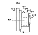
図2は、実施の形態1にかかるEL素子の構成図である。ここで、光源102の詳細な説明をする前に、図2を使用してEL素子についての説明をする。
【0044】
電界発光を利用したEL素子は、自己発光で、かつ完全固体素子である。このため、耐衝撃性にすぐれるなどの特徴を有することから、各種表示装置における発光素子としての利用が注目されている。
【0045】
このEL素子には、発光材料に無機化合物を用いてなる無機EL素子と有機化合物を用いてなる有機EL素子とがある。このうち、有機EL素子は、印加電圧を大幅に低くできるうえに、消費電力が小さい。また、有機EL素子は、小型化が容易であるうえに、面発光が可能であり、さらに三原色発光も容易である。このため、有機EL素子は、次世代の発光素子として研究開発が活発になされている。本発明では、有機EL素子を光源に採用している。
【0046】
EL素子104は、ガラス基板103上に、ITO(酸化インジウムにすずを混ぜたもの)である透明電極201、発光層202、Mg(マグネシウム)/Ag(銀)などである背面電極203を順次積層して作成されている。
【0047】
ガラス基板103は、発光した光を透過するような透明度を持ったガラスで構成されている。また、生産性、コスト面を考えてガラス基板103の厚さは1mm前後にされている。
【0048】
発光層202は、マイナスの電荷(電子)が流れやすい電子輸送層204とプラスの電荷(電子の抜け穴である正孔)が流れやすい正孔輸送層205からなる。
【0049】
正孔輸送層205は、透明電極201と接し、電子輸送層204は、背面電極203と接するように積層されている。電子輸送層204と正孔輸送層205を合わせた厚さは、千分の1mm以下である。
【0050】
次に、EL素子104の発光動作について図2を使用して説明する。
【0051】
背面電極203側をマイナスに、透明電極201側をプラスに直流電圧をかけると、背面電極203からはマイナスの電荷をもつ電子が電子輸送層204に流れ込み、透明電極201側から正孔が正孔輸送層205に流れ込む。電子と正孔は電子輸送層204と正孔輸送層205の接合面に達し、この界面でマイナスの電子とプラスの正孔はお互い引き付けあい、ちょうど電子が抜け殻である正孔を埋めるように接合する。この結合を電子が正孔と再結合するという。この時、電子のエネルギーが光の形で放出される。
【0052】
このように、EL素子104は、有機薄膜に電気を加えてプラスとマイナスの直流電流を流すことによって発光する。また、印加される直流電圧は10〜15Vであるため、一般のカラー画像読取装置では容易に使用できる電圧である。
【0053】
また、カラー画像読取装置の光源は、R/G/Bの光を切り替えて発光させるために、高速な応答速度が要求されている。しかし、EL素子104は、発光素子の応答速度、つまり電圧を印加してから、発光するまでの時間、電圧を切ってから消灯するまでの時間が百万分の一秒と非常に高速である。このため、EL素子104はカラー画像読取装置の光源には非常に適している。
【0054】
図3は、実施の形態1にかかる光源の構成を説明するための拡大断面図である。この図を使用して、実施の形態1にかかる光源について詳細に説明する。
【0055】
光源102は、ガラス基板103にEL素子104R,104G,104Bが取付けられている構造になっている。
【0056】
EL素子104Rは赤の波長域の光を発するEL素子であり、EL素子104Gは緑の波長域の光を発するEL素子であり、EL素子104Bは青の波長域の光を発するEL素子である。
【0057】
このような構成により、光源102は、EL素子104R,104G,104Bから発せられる光によって、赤、緑、青の光をガラス基板103を介して発光するようになっている。
【0058】
また、このように、光源102から発せられる光の色に三原色を適用することで、光の色の差別が明確になるので、色分離されたカラー画像の読取を効果的にできる。
【0059】
図4は、実施の形態1にかかる光源の上面図である。この図を使用して、どのように光源102にEL素子104R,104G,104Bが設けられているか説明する。
【0060】
光源102のガラス基板103上には、EL素子104R,104G,104Bが原稿の幅方向に配列してある。読取る原稿がA4原稿(210mmから216mm)のときには、ガラス基板103に配置されるEL素子104R,104G,104Bの長さ401は、230mm程度が最適な長さとなる。この長さ401は、装置の大きさに悪影響を与えず、原稿をむらなく照明できる長さである。この長さ401が原稿の幅より長くなっているのは、原稿をむらなく照明するために、直接上から照射される光だけでなく反射光も考慮にいれる必要が有るために、原稿の外からも光を照射しなくてはならないからである。また、A3原稿など他のサイズの原稿用の光源も同様の考え方で寸法を決めることができる。
【0061】
また、EL素子104Rの幅402R,EL素子104Gの幅402G,EL素子104Bの幅402Bは、同じになっている。
【0062】
しかしながら、EL素子104R,104G,104Bの発光効率や、レンズや、イメージセンサの各々の波長特性や分解能が異なる。このため、EL素子104R,104G,104Bの幅を変えてこれらの特性差を補うことを考えて、EL素子104R,104G,104Bの幅の最適化すると、様々な変形例が考えられる。
【0063】
図5は、実施の形態1にかかる光源の変形例の上面図である。この変形例は青の発光体が他の色の発光体より発光効率が低いことを考えたものである。またイメージセンサの感度も青の光に対しては、他の色より低くなっている。
【0064】
変形例の光源102aには、EL素子104R,EL素子104G,EL素子104Bが長さ401で配列してある。この長さ401は、図4の長さ401と同一である。
【0065】
光源102aに配列されたEL素子104Bの幅501Bの幅は、EL素子104Rの幅501R,EL素子104Gの幅501Gよりも広くなっている。このため、EL素子104Bの表面積が他のEL素子104R、104Gの表面積より大きくなっている。このように、EL素子104Bの表面積を大きくすることで他の色の発光体より発光効率が低いことを補うことができる。
【0066】
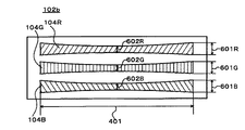
図6は、実施の形態1にかかる光源の縮小光学系に用いる変形例の上面図である。この変形例では、レンズのコサイン4乗則の特性により、レンズの周辺部がレンズの中央より暗くなる特性を考慮している。
【0067】
この変形例の光源102bには、EL素子104R,EL素子104G,EL素子104Bが長さ401で配列してある。この長さ401は、図4の長さ401と同一である。
【0068】
光源102bに配列されたEL素子104Rの端部の幅601R,EL素子104Gの端部の幅601G、EL素子104Bの端部の幅601Bは、EL素子104Rの中央の幅602R,EL素子104Gの中央の幅602G,EL素子104Bの中央の幅602Bよりも広くなっている。
【0069】
このような構成にすることにより、EL素子104R、104G、104Bの端部の発光効率があがるので、レンズを介しても原稿をむらなく照射することができる。
【0070】
上記のように、光源の形態については様々な変形例が考えられるが、以下の実施の形態1の説明では図4の光源を採用する。
【0071】
以下、実施の形態1にかかる画像読取処理のカラー画像読取動作について説明する。
【0072】
図7は、実施の形態1にかかる光源の各EL素子の点灯時間の制御を説明するためのタイミング図である。図1および図7を使用して、光源102の動作および実施の形態1にかかる読取り動作について説明する。
【0073】
まず、t0において、EL素子104Rに電圧をかけて点灯させて、赤色の光線109Rを原稿に照明する。
【0074】
この光線109Rは、ガラス基板103を透過して原稿101に達し、原稿101で反射され反射光110となる。この反射光110は、レンズ105に入射し、レンズ105によって結像された光線111になり、イメージセンサ106に結像される。
【0075】
光線111は、イメージセンサ106で光の強さに応じた電気信号に光電変換され、電気信号112として出力される。この電気信号112は図示しないA/D変換器でデジタル化され画像データとなる。このようにして原稿101の赤色に対応した部分の画像情報が得られる。
【0076】
t1において、EL素子104Rにかかる電圧を0にし発光を停止するとともに、EL素子104Gに電圧をかけて点灯させて、緑色の光線109Gを原稿に照明する。その後の処理については、EL素子104Rから光線109Rが原稿101に照射された場合と同じなので説明を省略する。
【0077】
このように、EL素子104Gから光線109Gが原稿に照射されることで原稿101の緑色に対応した画像情報が得られる。
【0078】
t2において、EL素子104Gにかかる電圧を0にし発光を停止するとともに、EL素子104Bに電圧をかけて点灯させて、青色の光線109Bを原稿に照明する。その後の処理については、EL素子104R、104Gから光線109R、109Gが原稿101に照射された場合と同じなので説明を省略する。
【0079】
このように、EL素子104Bから光線109Bが原稿に照射されることで原稿101の青色に対応した画像情報が得られる。
【0080】
t3において、EL素子104Bにかかる電圧を0にし発光を停止する。また、t0〜t1間、t1〜t2間、t2〜t3間の時間はすべて同じΔtである。
【0081】
しかし、光源102は、EL素子104Bが他のEL素子104R、104Gと比較して原稿に光を照射する位置に最も近く配置されている。このようにして、EL素子104Bの発光効率が低いことを補っている。
【0082】
すべてのEL素子104R、104G、104Bの発光時間を同じにしているが、EL素子104Bを原稿101の照射位置に最も近く配置しているため、EL素子104Bの発光効率が他のEL素子104R、104Gより低いことは補われている。
【0083】
このように、原稿101の各色に対応した画像情報が得られたら、次に原稿101はローラ107a,107bにより、矢印108の方向に送られ、次の原稿の位置の画像情報を読取る。
【0084】
この処理を繰り返すことにより、原稿101全体のカラー画像情報を読取られる。
【0085】
また、EL素子104R,104G,104Bの発光効率を考えて、EL素子104R,104G,104Bの点灯時間制御を最適化することも考えられる。
【0086】
図8は、実施の形態1にかかる光源の各EL素子の点灯時間の制御の変形例を説明するためのタイミング図である。
【0087】
この変形例では、EL素子104Bの照射をt2からt4の間にしている。この間の時間は2Δtとなっている。このように、発光効率の悪いEL素子104Bの照射時間を長くすることにより、EL素子104Bの発光効率が他のEL素子104R,104Gより悪いことを補うことができる。
【0088】
なお、図8では、EL素子104Bの照射時間を2Δtとしたが、EL素子104Bの発光効率を考慮し、照射時間を2Δt以外にすることも可能である。
【0089】
以上説明したように、実施の形態1は光源にEL素子を用いるので、光源が大幅に小型化される。また、従来の蛍光灯を用いた光源に必要であったインバータなどの装置が不用になる。よって、カラー画像読取装置全体の実装体積やコストが大幅に低減される。
【0090】
また、EL素子104R,104G,140Bは面発光するために、光源にLEDを用いた場合に必要な、ライトガイドも必要無くなる。
【0091】
また、実施の形態1によれば、EL素子の発光色による発光効率を補えるので、読取能力の低下も防止できる。
【0092】
さらに、実施の形態1では、主に光源に図4の光源、光源の制御は図7の方法を用いて説明したが、光源に図5または図6の光源、光源の制御に図8の方法を適用、または、これらを組み合わせることででEL素子の発光色による発光効率を効果的に補うことができる。
【0093】
(実施の形態2)
図9は、本発明の実施の形態2にかかるカラー画像読取装置の構成を示している図である。この図を使用して、実施の形態2にかかるカラー画像読取装置について詳細に説明する。なお、既に説明したものについては同一の符号を付与してある。
【0094】
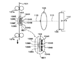
実施の形態2は、光源901を除いて実施の形態1と同じ構成である。
【0095】
光源901は、ガラス基板103が原稿101と平行に、かつ近接して配置されている。実際には、光源901と原稿101との距離は、1mm程度になっている。
【0096】
このため、実施の形態1に比べて大幅な発光効率の向上がなされている。また、光源901と原稿101との距離が近いため、カラー画像読取装置が小型化されている。
【0097】
図10は、実施の形態2にかかる光源の上面図である。この図を使用して実施の形態2にかかる光源の構成について詳細に説明する。すでに説明したものと同一のものには同一の符号を付与してある。
【0098】
光源901は、中心線901を挟んでEL素子104Bが二本設けられている。さらに、光源901は、原稿の読み取り点に近い位置にEL素子104Bを配置している。このため、EL素子104Bの発光効率が、他のEL素子104R,104Gより低いことが補われている。
【0099】
次に、実施の形態2にかかる画像記録装置の動作について図9を使用して説明する。
【0100】
EL素子104R,104G,104Bの制御については、実施の形態1と同様であるので省略する。
【0101】
光源901から発せられた光は、ガラス基板103を介して原稿101の読み取り位置に照射される。この光は、原稿101から反射して、光源901のガラス基板103の中心位置、つまり図10の中心線901を介してレンズ105に到達する。
【0102】
その後の動作については実施の形態1と同様なので省略する。
【0103】
このように実施の形態2では、原稿から反射した光を、光源のガラス基板を通してレンズに到達するようにしたため、光源を原稿に近づけることが可能になった。このため、カラー画像読取装置を小型化することができるとともに、光源の原稿に対する照射効率を向上することができる。
【0104】
また、青色の光を発光するEL素子を複数、かつ原稿の読み取り位置に近く設けることにより、青色の光を発光するEL素子の発光効率が低いことを補える。
【0105】
さらに、光源に配置するEL素子の幅を図5、図6のように変えたり、図7に示されるように照射時間を変えることを併用することで、より一層青色の光を発光するEL素子の発光効率が低いことを補える。
【0106】
なお、各EL素子の点灯時間の制御の図8に記載のタイミングを採用することにより、青色の光を発光するEL素子の発光効率が低いことを効果的に補える。
【0107】
(実施の形態3)
実施の形態3では、EL素子を使った光源を密着イメージセンサに適用している。
【0108】
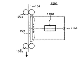
図11は、実施の形態3にかかる密着イメージセンサの構成を示す図である。なお、既に説明したものと同一のものには同一の符号を付与してある。
【0109】
密着イメージセンサ1101が、実施の形態1または実施の形態2で説明したような縮小光学系の画像読み取り装置と異なるのは、原稿101の幅と同一の幅の長さを持つ横長形状のイメージセンサ1102を持つ点と、イメージセンサ1102に原稿101からの反射光を結像するための等倍結像光学系のレンズアレイ1103を持つ部分が違う点である。その他の構成および動作については、実施の形態1と同一であるので省略する。
【0110】
このような密着型のイメージセンサ1101は、縮小光学系のセンサのような長い光路長が不要であるため、小型化される。また、イメージセンサ1102の画素サイズは読取りサイズと一致するため、高い感度が得られる。さらに、光源102、レンズ1103、イメージセンサ1102を一体構造にできるため、小型化されるだけでなく、装置調整上の利点もある。
【0111】
このように、EL素子を用いた光源102は、非常に小さく、直流の定電圧で点灯するため、密着イメージセンサ1101の光源として適している。また、EL素子の形状は図4のように原稿101と同じ、もしくは広くもできるので密着イメージセンナの光源として使いやすい。
【0112】
ここで、密着イメージセンサに実施の形態2で採用した光源を使用した変形例について説明する。
【0113】
図12は、実施の形態3にかかる密着イメージセンサの変形例の構成を示す図である。なお、既に説明したものと同一のものには同一の符号を付与してある。
【0114】
この例では、光源901を読み取りガラスとして使用している。よって、イメージセンサ1101よりもさらに構成が簡単になっている。また、原稿101と光源901との位置が非常に近いため、発光効率も向上している。
【0115】
【発明の効果】
以上説明したように、本発明によれば、光源にEL素子を用いて構成を簡略することにより小型化され、かつ読取能力が向上されたカラー画像読取装置を実現可能な画像読取装置を提供できる。
【図面の簡単な説明】
【図1】図1は、本発明の実施の形態1にかかるカラー画像読取装置の構成を示す図
【図2】実施の形態1にかかるEL素子の構成図
【図3】実施の形態1にかかる光源の構成を説明をするための拡大断面図
【図4】実施の形態1にかかる光源の上面図
【図5】実施の形態1にかかる光源の変形例の上面図
【図6】実施の形態1にかかる光源の縮小光学系に用いる変形例の上面図
【図7】実施の形態1にかかる光源の各EL素子の点灯時間の制御を説明するためのタイミング図
【図8】実施の形態1にかかる光源の各EL素子の点灯時間の制御の変形例を説明するためのタイミング図
【図9】本発明の実施の形態2にかかるカラー画像読取装置の構成を示す図
【図10】実施の形態2にかかる光源の上面図
【図11】本発明の実施の形態3にかかる密着イメージセンサの構成を示す図
【図12】実施の形態3にかかる密着イメージセンサの変形例の構成を示す図
【図13】従来のカラー画像読取装置の構成を示す図
【符号の説明】
101 原稿
102、901 光源
103 ガラス基板
104R、104G、104B エレクトロルミネッセンス素子(EL素子)
105、1103 レンズ
106、1102 イメージセンサ
1101、1201 密着イメージセンサ[0001]
BACKGROUND OF THE INVENTION
The present invention relates to an image reading apparatus using an electroluminescence element.
[0002]
[Prior art]
Conventionally, a color image reading apparatus has three light sources that emit light in a wavelength range of red (hereinafter referred to as R), green (hereinafter referred to as G), and blue (hereinafter referred to as B). Then, the color image information of the document is read by irradiating the document while sequentially switching the three light sources.
[0003]
FIG. 13 is a diagram showing a configuration of a conventional color image reading apparatus. A conventional image reading apparatus will be described with reference to FIG.
[0004]
First, the original 1301 to be read is illuminated by the
[0005]
In order to perform color reading, first, the
[0006]
In this way, the conventional image reading apparatus reads the color image data of the
[0007]
The
[0008]
[Problems to be solved by the invention]
However, a conventional color image reading apparatus has to perform high-frequency lighting in order to illuminate a document with a fluorescent lamp used as a light source. For this reason, an inverter is necessary for the conventional image reading apparatus. Therefore, the cost has increased and a space for mounting the inverter has been required.
[0009]
In order to uniformly illuminate the original, it is necessary to make the length of the fluorescent lamp longer than the width of the original in consideration of the fact that no light is emitted from the end of the fluorescent lamp. As an example, in order to illuminate a document width of A4 size (210 mm to 216 mm), a length of about 270 mm is required.
[0010]
Furthermore, since the fluorescent lamp has poor phosphor responsiveness, color switching cannot be performed at high speed. For this reason, a color image reading apparatus using a fluorescent lamp as a light source has a problem in that color separation is deteriorated and colors of a plurality of light beams are mixed. Therefore, it is difficult to perform high-speed reading in a color image reading apparatus using a fluorescent lamp as a light source.
[0011]
Conventionally, a form using an LED instead of a fluorescent lamp as a light source has been considered. However, an image reading apparatus using an LED as a light source has a problem that the LED has a low luminance and it is basically a point light source, so that it is difficult to obtain sufficient brightness. For this reason, it is considered that LEDs are arranged on a line to serve as a light source, but there has been a problem that the cost is increased.
[0012]
In order to solve this problem, it is also considered to use a form using an LED using a gallium nitride material having high luminance characteristics. However, LEDs using gallium nitride-based materials have a problem that they are very expensive compared to conventional LEDs. For this reason, it is considered to illuminate the entire document by arranging one to two LEDs of gallium nitride material at the end of a light guide system called a light guide. However, there is a problem that the configuration is complicated, and there is also a problem that a large amount of light cannot be obtained because there are few LEDs to be used.
[0013]
Further, as described in JP-A-6-284257, a form using an electroluminescence element (hereinafter referred to as an EL element) as a light source has been proposed. However, this publication only discloses monochrome image reading, and does not disclose any method applied to color image reading, and does not disclose a method using an EL element for color image reading.
[0014]
In addition, since the EL element has different light emission efficiency depending on the color of light emitted, it becomes a problem to compensate for the difference in light emission efficiency depending on the light emission color of the EL element.
[0015]
The present invention has been made in view of the above points, and is an image reading apparatus capable of realizing a color image reading apparatus that is reduced in size and improved in reading capability by using an EL element as a light source and simplifying the configuration. The purpose is to provide.
[0016]
[Means for Solving the Problems]
The present inventionIt has electroluminescent elements that emit red, green, and blue primary colors for illuminating the document, and electroluminescent elements that emit blue with low luminous efficiency are arranged on both sides of the center line on the transparent substrate. A light source in which an electroluminescent element that emits another color is arranged on the side opposite to the center line of the arranged electroluminescent element that emits blue, and the translucent substrate is arranged in parallel and close to the read document; An image sensor that photoelectrically converts reflected light from the document and reads image information of the document by the photoelectrically converted electrical signal, and the light source controls the electroluminescence element to control the color of light. Irradiating light to the reading position of the document through the translucent substrate while sequentially switching the image sensor, A configuration read sequentially switching the reflected light incident transmitted through the centerline of the translucent substrate from the reading position of the document for each color of light emitted to the document.
[0017]
By using an electroluminescence element as a light source in this way, the configuration of the image reading apparatus is simplified and downsized. Further, the ability to read a color image is improved by effectively irradiating the original with light utilizing the characteristic that the electroluminescence element emits light.
[0018]
DETAILED DESCRIPTION OF THE INVENTION
An image reading apparatus according to a first aspect of the present invention includes:It has electroluminescent elements that emit red, green, and blue primary colors for illuminating the document, and electroluminescent elements that emit blue with low luminous efficiency are arranged on both sides of the center line on the transparent substrate. A light source in which an electroluminescent element that emits another color is arranged on the side opposite to the center line of the arranged electroluminescent element that emits blue, and the translucent substrate is arranged in parallel and close to the read document; An image sensor that photoelectrically converts reflected light from the document and reads image information of the document by the photoelectrically converted electrical signal, and the light source controls the electroluminescence element to control the color of light. Irradiating light to the reading position of the document through the translucent substrate while sequentially switching the image sensor, A configuration read sequentially switching the reflected light incident transmitted through the centerline of the translucent substrate from the reading position of the document for each color of the light irradiated to the document.
[0019]
By using the electroluminescence element as the light source in this way, the configuration of the image reading apparatus that reads the color image information of the original is simplified and miniaturized.
[0020]
Further, with this configuration, the color image information separated for each color irradiated from the light source to the original can be read reliably, so that the color image data of the original can be read reliably.
[0022]
Also,With this configuration, not only can the light source be effectively downsized, but the light source can be placed in close contact with the document. For this reason, the image reading capability can be improved.
[0024]
Also,With this configuration, light of a color with low light emission efficiency can be strongly applied to the document, so that a difference in luminance applied to the document according to the color can be eliminated. For this reason, the color image reading ability of the document is improved.
[0027]
First of the present invention2The aspect of the firstAspectIn the image reading device,The width of the end portion of the electroluminescence element is wider than the width of the central portion..
[0029]
Hereinafter, embodiments of the present invention will be described in detail with reference to the drawings.
[0030]
The present invention employs an electroluminescence element (hereinafter referred to as EL element) as a light source of a color image reading apparatus. As a configuration using an EL element as a light source of a color image reading apparatus, (1) a system in which red, green, and blue elements are arranged like a CRT such as a TV, (2) a system in which white light emission and a color filter are combined, (3) A method of combining blue light emission and a color conversion layer can be considered.
[0031]
The method (1) does not use a color conversion layer like the method (2) or the method (3), and the use efficiency of light emission is good. Therefore, in the present invention, the method (1) will be mainly described.
[0032]
(Embodiment 1)
FIG. 1 is a diagram showing a configuration of a color image reading apparatus according to Embodiment 1 of the present invention. The color image reading apparatus according to the first embodiment will be described in detail with reference to FIG.
[0033]
The original 101 to be read is irradiated with light from the
[0034]
The
[0035]
Further, the
[0036]
Since the
[0037]
The
[0038]
The
[0039]
The
[0040]
Further, since the three primary colors are applied to the color of light emitted from the
[0041]
The
[0042]
Hereinafter, the
[0043]
FIG. 2 is a configuration diagram of the EL element according to the first embodiment. Here, before describing the
[0044]
An EL element using electroluminescence is self-luminous and a completely solid element. For this reason, since it has characteristics such as excellent impact resistance, it is attracting attention as a light emitting element in various display devices.
[0045]
This EL element includes an inorganic EL element using an inorganic compound as a light emitting material and an organic EL element using an organic compound. Of these, the organic EL element can significantly reduce the applied voltage and consumes less power. In addition, the organic EL element can be easily downsized, can emit surface light, and can easily emit three primary colors. For this reason, organic EL elements have been actively researched and developed as next-generation light-emitting elements. In the present invention, an organic EL element is used as a light source.
[0046]
The
[0047]
The
[0048]
The
[0049]
The
[0050]
Next, the light emission operation of the
[0051]
When a DC voltage is applied with the
[0052]
As described above, the
[0053]
Further, the light source of the color image reading device is required to have a high response speed in order to switch R / G / B light to emit light. However, the
[0054]
FIG. 3 is an enlarged cross-sectional view for explaining the configuration of the light source according to the first embodiment. The light source concerning Embodiment 1 is demonstrated in detail using this figure.
[0055]
The
[0056]
The
[0057]
With such a configuration, the
[0058]
Further, by applying the three primary colors to the color of light emitted from the
[0059]
FIG. 4 is a top view of the light source according to the first embodiment. Using this figure, how the
[0060]
On the
[0061]
The
[0062]
However, the light emission efficiency of the
[0063]
FIG. 5 is a top view of a modification of the light source according to the first embodiment. In this modification, the blue light emitter is considered to have lower luminous efficiency than the other color light emitters. The sensitivity of the image sensor is lower than other colors for blue light.
[0064]
In the
[0065]
A width 501B of the
[0066]
FIG. 6 is a top view of a modification used in the reduction optical system of the light source according to the first embodiment. In this modification, due to the characteristic of the cosine fourth power rule of the lens, the characteristic that the peripheral portion of the lens becomes darker than the center of the lens is considered.
[0067]
In the
[0068]
The
[0069]
With such a configuration, the light emission efficiency of the end portions of the
[0070]
As described above, various modifications of the light source are conceivable. In the following description of the first embodiment, the light source shown in FIG. 4 is adopted.
[0071]
Hereinafter, a color image reading operation of the image reading process according to the first embodiment will be described.
[0072]
FIG. 7 is a timing chart for explaining the control of the lighting time of each EL element of the light source according to the first embodiment. The operation of the
[0073]
First, at t0, a voltage is applied to the
[0074]
The light beam 109 </ b> R passes through the
[0075]
The
[0076]
At t1, the voltage applied to the
[0077]
Thus, image information corresponding to the green color of the
[0078]
At t2, the voltage applied to the
[0079]
In this manner, the image information corresponding to the blue color of the
[0080]
At t3, the voltage applied to the
[0081]
However, the
[0082]
Although the light emission times of all the
[0083]
Thus, when image information corresponding to each color of the original 101 is obtained, the original 101 is then sent in the direction of the
[0084]
By repeating this process, the color image information of the
[0085]
It is also conceivable to optimize the lighting time control of the
[0086]
FIG. 8 is a timing diagram for explaining a modification of the lighting time control of each EL element of the light source according to the first embodiment.
[0087]
In this modification, the
[0088]
In FIG. 8, the irradiation time of the
[0089]
As described above, since the first embodiment uses an EL element as a light source, the light source is significantly reduced in size. In addition, an inverter or other device that is necessary for a light source using a conventional fluorescent lamp becomes unnecessary. Therefore, the mounting volume and cost of the entire color image reading apparatus are greatly reduced.
[0090]
Further, since the
[0091]
Further, according to the first embodiment, since the light emission efficiency by the light emission color of the EL element can be supplemented, the reading ability can be prevented from being lowered.
[0092]
Further, in the first embodiment, the light source of FIG. 4 is mainly used as the light source and the control of the light source is described using the method of FIG. 7, but the light source of FIG. 5 or 6 is used as the light source, and the method of FIG. By applying or combining these, it is possible to effectively supplement the light emission efficiency of the light emission color of the EL element.
[0093]
(Embodiment 2)
FIG. 9 is a diagram showing a configuration of a color image reading apparatus according to the second embodiment of the present invention. The color image reading apparatus according to the second embodiment will be described in detail with reference to FIG. In addition, the same code | symbol is provided about what has already been demonstrated.
[0094]
The second embodiment has the same configuration as that of the first embodiment except for the
[0095]
In the
[0096]
For this reason, the luminous efficiency is greatly improved as compared with the first embodiment. Further, since the distance between the
[0097]
FIG. 10 is a top view of the light source according to the second embodiment. The configuration of the light source according to the second embodiment will be described in detail with reference to FIG. The same reference numerals are given to the same components as already described.
[0098]
The
[0099]
Next, the operation of the image recording apparatus according to the second embodiment will be described with reference to FIG.
[0100]
Since control of the
[0101]
Light emitted from the
[0102]
Since the subsequent operation is the same as that of the first embodiment, the description thereof is omitted.
[0103]
As described above, in the second embodiment, the light reflected from the original reaches the lens through the glass substrate of the light source, so that the light source can be brought close to the original. For this reason, it is possible to reduce the size of the color image reading apparatus and to improve the irradiation efficiency of the light source on the document.
[0104]
In addition, by providing a plurality of EL elements that emit blue light and close to the reading position of the original, it is possible to compensate for the low luminous efficiency of the EL elements that emit blue light.
[0105]
Furthermore, by changing the width of the EL element arranged in the light source as shown in FIGS. 5 and 6 or changing the irradiation time as shown in FIG. 7, an EL element that emits more blue light. Can compensate for the low luminous efficiency.
[0106]
By adopting the timing shown in FIG. 8 for controlling the lighting time of each EL element, it is possible to effectively compensate for the low luminous efficiency of the EL element that emits blue light.
[0107]
(Embodiment 3)
In Embodiment 3, a light source using an EL element is applied to the contact image sensor.
[0108]
FIG. 11 is a diagram illustrating a configuration of the contact image sensor according to the third embodiment. In addition, the same code | symbol is provided to the same thing as already demonstrated.
[0109]
The
[0110]
Such a contact-
[0111]
Thus, the
[0112]
Here, a modification using the light source employed in the second embodiment for the contact image sensor will be described.
[0113]
FIG. 12 is a diagram illustrating a configuration of a modified example of the contact image sensor according to the third embodiment. In addition, the same code | symbol is provided to the same thing as already demonstrated.
[0114]
In this example, the
[0115]
【The invention's effect】
As described above, according to the present invention, it is possible to provide an image reading apparatus capable of realizing a color image reading apparatus that is reduced in size and improved in reading ability by simplifying the configuration using an EL element as a light source. .
[Brief description of the drawings]
FIG. 1 is a diagram illustrating a configuration of a color image reading apparatus according to a first embodiment of the present invention.
FIG. 2 is a configuration diagram of an EL element according to the first embodiment.
FIG. 3 is an enlarged sectional view for explaining the configuration of the light source according to the first embodiment;
FIG. 4 is a top view of the light source according to the first embodiment.
FIG. 5 is a top view of a modification of the light source according to the first embodiment.
FIG. 6 is a top view of a modification used in the reduction optical system of the light source according to the first embodiment.
FIG. 7 is a timing chart for explaining control of lighting time of each EL element of the light source according to the first embodiment;
FIG. 8 is a timing chart for explaining a modification of the lighting time control of each EL element of the light source according to the first embodiment;
FIG. 9 is a diagram showing a configuration of a color image reading apparatus according to a second embodiment of the present invention.
FIG. 10 is a top view of a light source according to the second embodiment.
FIG. 11 is a diagram showing a configuration of a contact image sensor according to a third embodiment of the present invention.
FIG. 12 is a diagram showing a configuration of a modified example of the contact image sensor according to the third embodiment.
FIG. 13 is a diagram showing a configuration of a conventional color image reading apparatus.
[Explanation of symbols]
101 manuscript
102,901 Light source
103 Glass substrate
104R, 104G, 104B Electroluminescence element (EL element)
105, 1103 lenses
106, 1102 Image sensor
1101, 1201 Contact image sensor
Claims (2)
Priority Applications (1)
| Application Number | Priority Date | Filing Date | Title |
|---|---|---|---|
| JP16321999A JP4091712B2 (en) | 1999-06-10 | 1999-06-10 | Image reading device |
Applications Claiming Priority (1)
| Application Number | Priority Date | Filing Date | Title |
|---|---|---|---|
| JP16321999A JP4091712B2 (en) | 1999-06-10 | 1999-06-10 | Image reading device |
Publications (3)
| Publication Number | Publication Date |
|---|---|
| JP2000354132A JP2000354132A (en) | 2000-12-19 |
| JP2000354132A5 JP2000354132A5 (en) | 2006-06-01 |
| JP4091712B2 true JP4091712B2 (en) | 2008-05-28 |
Family
ID=15769583
Family Applications (1)
| Application Number | Title | Priority Date | Filing Date |
|---|---|---|---|
| JP16321999A Expired - Lifetime JP4091712B2 (en) | 1999-06-10 | 1999-06-10 | Image reading device |
Country Status (1)
| Country | Link |
|---|---|
| JP (1) | JP4091712B2 (en) |
Families Citing this family (8)
| Publication number | Priority date | Publication date | Assignee | Title |
|---|---|---|---|---|
| JP2002325162A (en) * | 2001-02-22 | 2002-11-08 | Matsushita Electric Ind Co Ltd | Light source for image reading apparatus and image reading apparatus |
| CN100423532C (en) * | 2001-08-09 | 2008-10-01 | 松下电器产业株式会社 | Light for image pickup device and driving device therefor |
| JP2006107755A (en) * | 2004-09-30 | 2006-04-20 | Seiko Epson Corp | Electrooptical device, image forming device and image reading device |
| JP4581692B2 (en) * | 2005-01-11 | 2010-11-17 | セイコーエプソン株式会社 | ORGANIC LIGHT EMITTING DIODE DEVICE, IMAGE FORMING DEVICE, AND IMAGE READING DEVICE |
| JP4742624B2 (en) * | 2005-03-04 | 2011-08-10 | セイコーエプソン株式会社 | ELECTRO-OPTICAL DEVICE, MANUFACTURING METHOD THEREOF, IMAGE PRINTING DEVICE, AND IMAGE READING DEVICE |
| JP4902573B2 (en) * | 2008-02-25 | 2012-03-21 | 株式会社リコー | Image reading device |
| JP4766066B2 (en) | 2008-03-14 | 2011-09-07 | コニカミノルタビジネステクノロジーズ株式会社 | Image reading apparatus and light source |
| JP6340793B2 (en) | 2013-12-27 | 2018-06-13 | セイコーエプソン株式会社 | Optical device |
Family Cites Families (7)
| Publication number | Priority date | Publication date | Assignee | Title |
|---|---|---|---|---|
| JPS56161773A (en) * | 1980-05-16 | 1981-12-12 | Hitachi Ltd | Arraying device of photosensor |
| JPS61131960A (en) * | 1984-11-30 | 1986-06-19 | Sharp Corp | Color picture reader |
| JPS6482758A (en) * | 1987-09-24 | 1989-03-28 | Minolta Camera Kk | Color image reader |
| JPH03107861U (en) * | 1990-02-21 | 1991-11-06 | ||
| JPH05191563A (en) * | 1991-02-27 | 1993-07-30 | Ricoh Co Ltd | Picture reader |
| JPH05328025A (en) * | 1992-05-27 | 1993-12-10 | Canon Inc | Original reader |
| JPH0879446A (en) * | 1994-09-08 | 1996-03-22 | Seiko Epson Corp | Image input device |
-
1999
- 1999-06-10 JP JP16321999A patent/JP4091712B2/en not_active Expired - Lifetime
Also Published As
| Publication number | Publication date |
|---|---|
| JP2000354132A (en) | 2000-12-19 |
Similar Documents
| Publication | Publication Date | Title |
|---|---|---|
| KR100379243B1 (en) | Linear illumination device | |
| JP2001135479A (en) | Light-emitting element and image-reading device using it, information-processing device and display device | |
| TW201044568A (en) | Non-radiatively pumped wavelength converter | |
| JP4091712B2 (en) | Image reading device | |
| WO2006107011A1 (en) | Light-emitting unit, illuminating device using such light-emitting unit, and image scanner | |
| JP2006197531A (en) | Method of scanning image scanner | |
| JP2012502489A (en) | LED projector | |
| US9001394B2 (en) | Image scanning apparatus and control method thereof | |
| US8610978B2 (en) | Document reading apparatus | |
| JP2008071664A (en) | Electro-optical device and electronic equipment | |
| JP2002351359A (en) | Led array and led display device | |
| JPH05191563A (en) | Picture reader | |
| JP2000354132A5 (en) | ||
| JP3956963B2 (en) | Image reading device | |
| US7315405B2 (en) | Image forming apparatus and image scanning method | |
| US20030142208A1 (en) | Image reading apparatus | |
| JPH05328025A (en) | Original reader | |
| JP2004120743A (en) | Light source | |
| JP3575394B2 (en) | Linear lighting device | |
| JPS58212255A (en) | Reader of color original | |
| JP2001292280A (en) | Illuminator and image reader to use the same | |
| JP5059327B2 (en) | Illumination device for image reading apparatus | |
| TW475325B (en) | Scanner having OLED | |
| JPH11136451A (en) | Illumination device and information processor using the same | |
| JP2009094960A (en) | Image reader |
Legal Events
| Date | Code | Title | Description |
|---|---|---|---|
| A521 | Request for written amendment filed |
Free format text: JAPANESE INTERMEDIATE CODE: A523 Effective date: 20060410 |
|
| A621 | Written request for application examination |
Free format text: JAPANESE INTERMEDIATE CODE: A621 Effective date: 20060410 |
|
| A977 | Report on retrieval |
Free format text: JAPANESE INTERMEDIATE CODE: A971007 Effective date: 20071112 |
|
| A131 | Notification of reasons for refusal |
Free format text: JAPANESE INTERMEDIATE CODE: A131 Effective date: 20071120 |
|
| A521 | Request for written amendment filed |
Free format text: JAPANESE INTERMEDIATE CODE: A523 Effective date: 20080109 |
|
| TRDD | Decision of grant or rejection written | ||
| A01 | Written decision to grant a patent or to grant a registration (utility model) |
Free format text: JAPANESE INTERMEDIATE CODE: A01 Effective date: 20080205 |
|
| A61 | First payment of annual fees (during grant procedure) |
Free format text: JAPANESE INTERMEDIATE CODE: A61 Effective date: 20080229 |
|
| R150 | Certificate of patent or registration of utility model |
Free format text: JAPANESE INTERMEDIATE CODE: R150 |
|
| FPAY | Renewal fee payment (event date is renewal date of database) |
Free format text: PAYMENT UNTIL: 20110307 Year of fee payment: 3 |
|
| FPAY | Renewal fee payment (event date is renewal date of database) |
Free format text: PAYMENT UNTIL: 20110307 Year of fee payment: 3 |
|
| FPAY | Renewal fee payment (event date is renewal date of database) |
Free format text: PAYMENT UNTIL: 20120307 Year of fee payment: 4 |
|
| FPAY | Renewal fee payment (event date is renewal date of database) |
Free format text: PAYMENT UNTIL: 20130307 Year of fee payment: 5 |