JP4091702B2 - Error absorbing connector - Google Patents
Error absorbing connector Download PDFInfo
- Publication number
- JP4091702B2 JP4091702B2 JP37687398A JP37687398A JP4091702B2 JP 4091702 B2 JP4091702 B2 JP 4091702B2 JP 37687398 A JP37687398 A JP 37687398A JP 37687398 A JP37687398 A JP 37687398A JP 4091702 B2 JP4091702 B2 JP 4091702B2
- Authority
- JP
- Japan
- Prior art keywords
- housing
- contact
- sliding
- conductive member
- sliding housing
- Prior art date
- Legal status (The legal status is an assumption and is not a legal conclusion. Google has not performed a legal analysis and makes no representation as to the accuracy of the status listed.)
- Expired - Lifetime
Links
Images


Classifications
-
- H—ELECTRICITY
- H01—ELECTRIC ELEMENTS
- H01R—ELECTRICALLY-CONDUCTIVE CONNECTIONS; STRUCTURAL ASSOCIATIONS OF A PLURALITY OF MUTUALLY-INSULATED ELECTRICAL CONNECTING ELEMENTS; COUPLING DEVICES; CURRENT COLLECTORS
- H01R13/00—Details of coupling devices of the kinds covered by groups H01R12/70 or H01R24/00 - H01R33/00
- H01R13/62—Means for facilitating engagement or disengagement of coupling parts or for holding them in engagement
- H01R13/629—Additional means for facilitating engagement or disengagement of coupling parts, e.g. aligning or guiding means, levers, gas pressure electrical locking indicators, manufacturing tolerances
- H01R13/631—Additional means for facilitating engagement or disengagement of coupling parts, e.g. aligning or guiding means, levers, gas pressure electrical locking indicators, manufacturing tolerances for engagement only
- H01R13/6315—Additional means for facilitating engagement or disengagement of coupling parts, e.g. aligning or guiding means, levers, gas pressure electrical locking indicators, manufacturing tolerances for engagement only allowing relative movement between coupling parts, e.g. floating connection
-
- H—ELECTRICITY
- H01—ELECTRIC ELEMENTS
- H01R—ELECTRICALLY-CONDUCTIVE CONNECTIONS; STRUCTURAL ASSOCIATIONS OF A PLURALITY OF MUTUALLY-INSULATED ELECTRICAL CONNECTING ELEMENTS; COUPLING DEVICES; CURRENT COLLECTORS
- H01R13/00—Details of coupling devices of the kinds covered by groups H01R12/70 or H01R24/00 - H01R33/00
- H01R13/66—Structural association with built-in electrical component
Description
【0001】
【発明の属する技術分野】
本発明は、ピン形の相手側導通部材に接続されるコネクタの技術分野に属し、特にコネクタと相手側導通部材の位置関係が正規のときよりもずれているときに(以下、アライメント誤差があるときという)、これを吸収して接続できるようにした誤差吸収コネクタに関する。
【0002】
【従来の技術】
一般に、プリント配線板用コネクタとして、例えば実公平3−9255号公報に開示されるように、ハウジングにコンタクトを内装し、コンタクトの一端を実装部としてプリント配線板又はケース等のスルーホールに挿通してハンダ付けすると共に、筒形になったコンタクト他端の接続部にピン形の相手側導通部材を嵌入することにより、プリント配線板に相手側導通部材を機械的及び電気的に接続するようにしたものが広く用いられている。
【0003】
【発明が解決しようとする課題】
ところで、このようなコネクタを例えば二枚のプリント配線板等の接続(いわゆるボード・ツー・ボードの接続)に用いる場合、接続すべきコネクタ及び相手側導通部材が別々のプリント配線板等に実装されるが、二枚のプリント配線板等の位置関係が確定したときに、接続すべきコネクタと相手側導通部材の位置関係が正規の位置関係からずれてアライメント誤差が生じることがあり、この誤差が大きいとコネクタに相手側導通部材を接続することができない。これを強引に接続できたとしても、無理な姿勢で接続すればハンダ付け部等に過大な応力がかかってクラックが入るなどの不具合が起こり、接続不良をきたす。このようなアライメント誤差は、例えばボード・ツー・ボードの接続においてコネクタ及び相手側導通部材を多数実装し、これらを一括して接続するようにしたときに起こりやすく、プリント配線板等の組み付け作業が困難となる事態を招く。
【0004】
本発明はこのような点に着目してなされたものであり、その目的とするところは、ハウジングを実装側と接続側に分割して両者をコンタクトで浮動状態に連結し、接続側のハウジングを相手側導通部材と交差する面内で摺動可能とすることにより、アライメント誤差を有効に吸収して接続不能及び接続不良の発生を防止して信頼性を高めると共に、プリント配線板等の組み付け作業性を向上させ、コンタクトを相手側導通部材にハンダ付けしたときにハンダの垂れをなくして製品品質の向上を図ることにある。さらに、コンタクトの過大な変形を阻止して破損等の不具合を未然に防止することを目的とする。
【0005】
【課題を解決するための手段】
上記目的を達成するため、請求項1の誤差吸収コネクタは、ピン形の相手側導通部材に接続されるコネクタであって、ハウジングをベースハウジングと、このベースハウジングに対して相手側導通部材と交差する面内で摺動可能に支持された摺動ハウジングとにより構成し、コンタクトの一部をベースハウジングと摺動ハウジングとに架設すると共に、摺動ハウジングに、一端がコンタクトに臨んで開口し且つ他端が相手側導通部材に向かい末広がりになって開口するハウジング貫通孔を設け、ベースハウジングに、前方に向かって開放された断面略コ字形の挟持部が左右に離間して設けられ、この挟持部で摺動ハウジングが摺動可能に挟持されていると共に、接続片と実装片とにより略逆L字形に形成されたコンタクトにおける接続片が摺動ハウジングの上面に固定され、実装片がベースハウジングの前面に固定されることでコンタクトの一部がベースハウジングと摺動ハウジングとに架設されており、摺動ハウジングの上面にあるコンタクト接続片における上記ハウジング貫通孔の一端が臨む部位にコンタクト接続片を貫通するコンタクト貫通孔を設け、上記ハウジング貫通孔の下端が摺動ハウジングの下面に開口している。
【0006】
【0007】
【0008】
この誤差吸収コネクタは、コンタクト実装片の先端をプリント配線板等にハンダ付けすることで実装される。そして、相手側導通部材をハウジング貫通孔に挿入するとコンタクト貫通孔を通ることでコンタクトを貫通し、両者をハンダ付けさせれば接続が完了する。その場合、アライメント誤差により相手側導通部材とハウジング貫通孔のセンターが一致していなくても相手側導通部材はハウジング貫通孔の広い開口でひろわれ、ハウジング貫通孔を進むにしたがってコンタクトの弾性変形により摺動ハウジングがベースハウジングに対して相手側導通部材と交差する面内で摺動するので、相手側導通部材はコンタクトまで導かれて接続可能となる。また、コンタクトが撓む分だけハンダ付け部等にかかる応力が軽減されるので、ハンダ付け部にクラックが入るなどの不具合が回避される。さらに、相手側導通部材がハウジング貫通孔にひろわれてスムーズに入っていくので、プリント配線板等の組み付け作業性が向上する。加えて、コンタクトを貫通した相手側導通部材をコンタクトの上面にハンダ付けしたときには、ハンダの垂れが生じない。
【0009】
請求項2の誤差吸収コネクタは、請求項1の構成において、ベースハウジング挟持部間における摺動ハウジングに、摺動ハウジングの左右方向への移動により挟持部に係止される横ストッパが設けられ、ベースハウジングの上面及び摺動ハウジングの下面に、摺動ハウジングの前方への移動により係止する縦ストッパが設けられている。
【0010】
このようにすれば、横ストッパにより摺動ハウジングの左右方向の移動が規制され、縦ストッパにより摺動ハウジングの前方への移動が規制され、ベースハウジング挟持部により摺動ハウジングの後方への移動が規制されて可動範囲の限界が設定されるから、コンタクトの過大な変形が阻止される。
【0011】
【発明の実施の形態】
以下、本発明の実施の形態を図面に基づいて説明する。図1〜図5は第1の実施形態に係る誤差吸収コネクタを示す。この誤差吸収コネクタは、例えば図6に示すように、ケースCとプリント配線板Pを接続するときに、プリント配線板Pに実装されるものである。図6で例示したものでは、ケースCにピン形の相手側導通部材Bが上向きに突出するように実装されており、この相手側導通部材Bがプリント配線板Pに開口する連通窓Wから上に抜け出て誤差吸収コネクタ(図6では図示省略)に接続されるようになっている。
【0012】
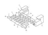
図1〜図5に示すように、第1実施形態のコネクタは、絶縁材料で構成されたハウジング1と、弾性を有する導電性材料で構成されたコンタクト2とを備えている。上記ハウジング1はベースハウジング3と、このベースハウジング3に対して相手側導通部材Bと交差する面内で摺動可能に支持された摺動ハウジング4とにより構成されている。ベースハウジング3には、前方に向かって開放された断面略コ字形の挟持部5、5が左右に離間して設けられ、この挟持部5、5により摺動ハウジング4が端部4b、4bにおいて摺動可能に挟持されている。
【0013】
コンタクト2は、一部がベースハウジング3と摺動ハウジング4とに架設されている。すなわち、コンタクト2は接続片2aと実装片2bとにより略逆L字形に形成され、接続片2aが摺動ハウジング4の上面に固定され、実装片2bがベースハウジング3の前面に固定されることでコンタクト2の一部がベースハウジング3と摺動ハウジング4とに架設されている。そして、コンタクト2はベースハウジング3と摺動ハウジング4の表面に刻設された溝3a、4aに嵌合している。また、図1に示すように、一部又は全部のコンタクト2の実装片2bには、先端付近を長手方向に湾曲形成することによりベント部2cが形成されており、このベント部2cがプリント配線板Pのスルーホールに入ると弾性変形し、その復元力によって誤差吸収コネクタをプリント配線板Pに仮止めするようにしている。さらに、図4(a)に示すように、コンタクト2の接続片2aには画像認識用の穴2dが形成されており、相手側導通部材Bと自動ハンダ付けするときに、ハンダ付け部分の位置を認識して自動ハンダ付け機の位置ずれ補正を行うようにしている。
【0014】
摺動ハウジング4には、一端がコンタクト2に臨んで開口し且つ他端が相手側導通部材Bに向かい末広がりになって開口するハウジング貫通孔6aが設けられている。摺動ハウジング4の上面にあるコンタクト接続片2aにおける上記ハウジング貫通孔6aの一端が臨む部位には、コンタクト接続片2aを貫通するコンタクト貫通孔6bが設けられている。また、上記ハウジング貫通孔6aの下端が摺動ハウジング4の下面に開口している。
【0015】
ベースハウジング3の挟持部5、5の間における摺動ハウジング4には、摺動ハウジング4が左右方向に移動したときに挟持部5、5に当接して係止される横ストッパ7、7が設けられている。また、ベースハウジング3の上面には縦ストッパ8が、そして摺動ハウジング4の下面には縦ストッパ9がそれぞれ突出して設けられ、摺動ハウジング4が前方に移動したときに互いに係止するようになっている。これらの縦ストッパ8、9は、摺動ハウジング4をベースハウジング3に組み付けるときに一方のストッパが他方のストッパを乗り越えることでハウジングの組み付けを可能としている。なお、10はベースハウジング3の下面から下方に突き出た補強用タブであって、必要に応じて設けられる。この補強用タブ10は、プリント配線板Pのスルーホールに挿入してハンダ付けされることで、誤差吸収コネクタのプリント配線板Pへの実装強度を上げるものである。
【0016】
従って、上記第1実施形態の誤差吸収コネクタは、図7(a)に示すように、コンタクト2の実装片2bの先端をプリント配線板Pにハンダ付けすることで実装される。そして、相手側導通部材Bをハウジング貫通孔6aに挿入するとコンタクト貫通孔6bを通ることでコンタクト2の接続片2aを貫通し、両者をハンダ付けさせれば接続が完了する。その場合、アライメント誤差により相手側導通部材Bとハウジング貫通孔6aのセンターが一致していなくても相手側導通部材Bはハウジング貫通孔6aの広い開口でひろわれ、ハウジング貫通孔6aを進むにしたがってコンタクト2の弾性変形により摺動ハウジング4がベースハウジング3に対して相手側導通部材Bと交差する面内で摺動するので、相手側導通部材Bはコンタクト2まで導かれて接続可能となる。このようにアライメント誤差を吸収できるので、コネクタと相手側導通部材Bとが接続不能となることを有効に防止してコネクタの信頼性を高めることができる。また、コンタクト2が撓む分だけハンダ付け部等にかかる応力が軽減されるので、ハンダ付け部にクラックが入るなどの不具合が回避され、接続不良の発生を防止してコネクタの信頼性を高めることができる。さらに、相手側導通部材Bがハウジング貫通孔6aにひろわれ、ハウジング貫通孔6aの奥へスムーズに入っていくので、プリント配線板Pの組み付け作業性が向上する。以上の効果は特にコネクタ及び相手側導通部材Bを多数実装し、これらを一括して接続するボード・ツー・ボードの接続を行うときに顕著である。
【0017】
また、接続片2aを摺動ハウジング4の上面に固定すると共に、コンタクト接続片2aにコンタクト貫通孔6bを設けたことから、コンタクト2を貫通した相手側導通部材Bをコンタクト2の上面にハンダ付けできるので、ハンダの垂れが生じない。その場合、図7(b)に示すように、単体のハウジング1’にコンタクト2’を取り付け、このコンタクト2’の先端を相手側導通部材Bに当ててハンダ付けする比較例に較べてみると、その効果が顕著であることが明らかである。
【0018】
さらに、本発明は横ストッパ7、7及び縦ストッパ8、9を設けない実施形態を含むが、上記第1実施形態のようにストッパ7、8、9を設けたときには横ストッパ7、7により摺動ハウジング4の左右方向の移動が規制され、縦ストッパ8、9により摺動ハウジング4の前方への移動が規制され、ベースハウジング挟持部5、5により摺動ハウジング4の端部4b、4bを受け止めてその後方への移動が規制され、これによって可動範囲の限界が設定されるから、コンタクト2の過大な変形が阻止され、破損等の不具合を未然に防止してコネクタの信頼性を高めることができる。
【0019】
また、先に図7(b)で示した比較例ではコンタクト2’が剥き出しで突出しているので、プリント配線板Pへの実装時及び相手側導通部材Bとの接続時に他部材等に当たり、コンタクト2’が曲がったり折れたりする不具合が起こる。これに対し、上記第1実施形態ではコンタクト2の接続片2aが摺動ハウジング4に固定され、実装片2bがベースハウジング3に固定されているので、そのような不具合がなく、コネクタと相手側導通部材Bとが接続不能となることを有効に防止することができる。さらに、本発明はコンタクトをそのままハウジングの表面に固定した実施形態を含むが、上記第1実施形態のようにハウジング3、4の表面に溝3a、4aを刻設し、この溝3a、4aにコンタクト2を嵌合したときには、コンタクト2が溝3a、4aに保護されるので上記不具合発生の更なる防止が図られ、コネクタと相手側導通部材Bとが接続不能となることを一層確実に防止してコネクタの信頼性を高めることができる。
【0020】
さらに、本発明はコンタクト2の実装片2bをストレートに形成してベント部を設けない実施形態を含むが、上記第1実施形態のようにコンタクト実装片2bにベント部2cを設けたときには、コンタクト2をプリント配線板Pに差し込むだけで誤差吸収コネクタをプリント配線板Pに仮止めして次工程へ運ぶことができる。このため、従来のようにプリント配線板Pからコネクタが落ちないようにプリント配線板Pに差し込んだコンタクトの先端を折曲げる工程を省くことができ、大量生産の効率が向上する。
【0021】
また、本発明はコンタクト2の接続片2aに画像認識用穴2dを形成しない実施形態を含むが、上記第1実施形態のように画像認識用穴2dを形成したときには、自動ハンダ付け機の位置ずれ補正ができるので、ハンダ付けの精度を上げて製品の歩留まりを向上させることができる。
【0022】
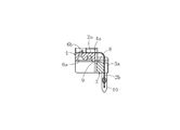
図8は第2の実施形態を示す。この第2実施形態が上記第1実施形態と構成を異にする点のみ説明する。ベースハウジング3の挟持部5の下面には小さな突起11が形成されていると共に、摺動ハウジング4の上面には上記突起11が嵌合するくぼみ12が凹陥形成されており、組み付け時に摺動ハウジング4をベースハウジング3に対して仮止めできるようになっている。このようにすれば、例えば摺動ハウジング4をベースハウジング3に対して正規の位置に仮固定した状態でプリント配線板Pに実装したときには、ハウジング貫通孔6aが相手側導通部材Bをひろう確率が高まり、アライメント誤差の吸収機能を高めることができる。
【0023】
図9は第3の実施形態を示す。この第3実施形態が上記第1実施形態と構成を異にする点のみ説明する。コンタクト2の接続片2aの先端側は幅方向の両端が立ち上がっていて断面が略コの字を寝かせた形になるように形成されているが、隣合うコンタクト2における上記略コ字状部分に挟まれた摺動ハウジング4の部位のなかでハンダ付けの対象となる付近は上部が削られていて、他の部位よりも低い肉抜き部4cが形成されている。こうすることにより、レーザービーム等により自動でハンダ付けするときに摺動ハウジング4のなかで焦げるおそれのある部位がなくなり、製品の信頼性を向上させて歩留まりを向上させることができる。
【0024】
上記実施形態はあくまで例示であり、本発明はこれによって限定されるものではない。本発明の誤差吸収コネクタは、プリント配線板やケース等に実装されるコネクタとして広く用いることができる。本発明では、挟持部の数は問題とならず、三箇所以上に設けてもよい。ハウジング貫通孔の一端がコンタクトに臨んで開口する実施形態として、ハウジング貫通孔の一端がコンタクトの端縁に接して開口する実施形態が例示される。また本発明は、以上の実施形態を適宜に組み合わせた実施形態を含む。
【0025】
【発明の効果】
以上説明したように、請求項1の誤差吸収コネクタによれば、ハウジング貫通孔で相手側導通部材をひろい、コンタクトの弾性変形により摺動ハウジングが摺動することでアライメント誤差を有効に吸収するので、コネクタと相手側導通部材とが接続不能となることを有効に防止することができ、また強引な接続によりハンダ付け部等に過大な応力がかかってクラックが入るなどの不具合をなくして接続不良の発生を防止することができ、コネクタの信頼性を高めることができると共に、プリント配線板等の組み付け作業性を向上させることができる。以上の効果は特にコネクタ及び相手側導通部材を多数実装し、これらを一括して接続するボード・ツー・ボードの接続を行うときに顕著である。また、コンタクトを貫通した相手側導通部材をコンタクトの上面にハンダ付けしたときに、ハンダの垂れが生じないようにすることができ、製品品質を高めることができる。
【0026】
【0027】
請求項2のようにすれば、請求項2で得られた効果に加えて、摺動ハウジングの前後左右の移動が規制されて可動範囲の限界が設定されるから、コンタクトの過大な変形を阻止して破損等の不具合を未然に防止してコネクタの信頼性を高めることができる。
【図面の簡単な説明】
【図1】 第1実施形態に係る誤差吸収コネクタの斜視図である。
【図2】 第1実施形態に係る誤差吸収コネクタのベースハウジング及び摺動ハウジングを示す分解斜視図である。
【図3】 第1実施形態に係る誤差吸収コネクタの摺動ハウジングにコンタクトを組み付けた状態で示す斜視図である。
【図4】 第1実施形態に係る誤差吸収コネクタを示し、(a)は平面図、(b)は正面図、(c)は底面図である。
【図5】 図4(b)におけるV−V線断面図である。
【図6】 第1実施形態に係る誤差吸収コネクタを用いて接続するケース及びプリント配線板を示す縮小斜視図である。
【図7】 コンタクトと相手側導通部材の接続状態を示す断面図であり、(a)は第1実施形態に係る誤差吸収コネクタの場合を、(b)は比較例の場合を示す。
【図8】 第2実施形態に係る誤差吸収コネクタの要部を示す拡大断面図である。
【図9】 第3実施形態に係る誤差吸収コネクタの斜視図である。
【符号の説明】
B 相手側導通部材
P プリント配線板
C ケース
1 ハウジング
2 コンタクト
2a 接続片
2b 実装片
3 ベースハウジング
3a 溝
4 摺動ハウジング
4a 溝
4b 端部
5 挟持部
6a ハウジング貫通孔
6b コンタクト貫通孔
7 横ストッパ
8 縦ストッパ
9 縦ストッパ[0001]
BACKGROUND OF THE INVENTION
The present invention belongs to the technical field of a connector connected to a pin-shaped mating conductive member, and particularly when the positional relationship between the connector and the mating conductive member is deviated from that of a normal one (hereinafter, there is an alignment error). The present invention relates to an error absorbing connector that absorbs this and can be connected.
[0002]
[Prior art]
Generally, as a printed wiring board connector, for example, as disclosed in Japanese Utility Model Publication No. 3-9255, a housing is provided with a contact, and one end of the contact is inserted into a through hole such as a printed wiring board or a case as a mounting portion. Soldering and inserting a pin-shaped mating member into the connecting part at the other end of the cylindrical contact so that the mating member is mechanically and electrically connected to the printed wiring board. Are widely used.
[0003]
[Problems to be solved by the invention]
By the way, when such a connector is used for connecting, for example, two printed wiring boards (so-called board-to-board connection), the connector to be connected and the mating conductive member are mounted on separate printed wiring boards. However, when the positional relationship between the two printed wiring boards is determined, the positional relationship between the connector to be connected and the mating conductive member may deviate from the normal positional relationship, resulting in an alignment error. If it is larger, the mating conductive member cannot be connected to the connector. Even if it can be forcibly connected, if it is connected in an unreasonable posture, problems such as excessive stress applied to the soldered portion and cracks occur, resulting in poor connection. Such an alignment error is likely to occur when, for example, a large number of connectors and mating conductive members are mounted in a board-to-board connection, and these are connected together. Invite difficult situations.
[0004]
The present invention has been made paying attention to such points, and the object of the present invention is to divide the housing into a mounting side and a connection side, and connect both in a floating state with a contact. By making it slidable in the plane that intersects with the mating conductive member, it effectively absorbs alignment errors, prevents connection failure and connection failure, improves reliability, and assembles printed wiring boards, etc. It is intended to improve product quality by eliminating solder dripping when a contact is soldered to a mating conductive member . It is another object of the present invention to prevent the contact from being deformed by preventing excessive deformation of the contact.
[0005]
[Means for Solving the Problems]
In order to achieve the above object, an error absorbing connector according to claim 1 is a connector connected to a pin-shaped mating conductive member, wherein the housing intersects the base housing and the mating conductive member with respect to the base housing. And a sliding housing supported so as to be slidable within the surface, and a part of the contact is installed on the base housing and the sliding housing, and one end of the contact faces the contact and opens. A housing through-hole is provided with the other end widening toward the mating conductive member, and a holding portion having a substantially U-shaped cross section that is open toward the front is provided on the base housing so as to be separated from the left and right. The sliding housing is slidably held between the contact pieces and the connection piece in the contact formed in a substantially inverted L shape by the connection piece and the mounting piece is slid. Since the mounting piece is fixed to the upper surface of the housing and the mounting piece is fixed to the front surface of the base housing, a part of the contact is installed between the base housing and the sliding housing. A contact through hole penetrating the contact connecting piece is provided at a portion facing one end of the housing through hole, and a lower end of the housing through hole is opened on a lower surface of the sliding housing.
[0006]
[0007]
[0008]
This error absorbing connector is mounted by soldering the tip of the contact mounting piece to a printed wiring board or the like. Then, when the counterpart conductive member is inserted into the housing through hole, the contact is passed through the contact through hole, and the connection is completed if both are soldered. In that case, even if the mating conduction member and the center of the housing through hole do not coincide due to an alignment error, the mating conduction member is expanded by the wide opening of the housing through hole, and due to the elastic deformation of the contact as it advances through the housing through hole Since the sliding housing slides with respect to the base housing in a plane intersecting with the mating conductive member, the mating conductive member is led to the contact and can be connected. Further, since the stress applied to the soldered portion is reduced by the amount of bending of the contact, problems such as cracks in the soldered portion are avoided. Furthermore, since the mating conductive member is smoothly inserted into the housing through-hole, the workability of assembling the printed wiring board and the like is improved. In addition, when the counterpart conductive member that penetrates the contact is soldered to the upper surface of the contact, no dripping of the solder occurs.
[0009]
According to a second aspect of the present invention, in the configuration of the first aspect , the error absorbing connector is provided with a lateral stopper that is locked to the holding portion by moving the sliding housing in the left-right direction on the sliding housing between the base housing holding portions, Vertical stoppers are provided on the upper surface of the base housing and the lower surface of the sliding housing to be locked by moving the sliding housing forward.
[0010]
By doing so, the lateral stopper restricts the movement of the sliding housing in the left-right direction, the longitudinal stopper restricts the movement of the sliding housing to the front, and the base housing clamping portion prevents the sliding housing from moving backward. Since the limit of the movable range is set by restriction, excessive deformation of the contact is prevented.
[0011]
DETAILED DESCRIPTION OF THE INVENTION
Hereinafter, embodiments of the present invention will be described with reference to the drawings. 1 to 5 show an error absorbing connector according to the first embodiment. For example, as shown in FIG. 6, the error absorbing connector is mounted on the printed wiring board P when the case C and the printed wiring board P are connected. In the example illustrated in FIG. 6, a pin-shaped mating conductive member B is mounted on the case C so as to protrude upward, and the mating conductive member B is located above the communication window W opening in the printed wiring board P. And is connected to an error absorbing connector (not shown in FIG. 6).
[0012]
As shown in FIGS. 1-5, the connector of 1st Embodiment is provided with the housing 1 comprised with the insulating material, and the
[0013]
A part of the
[0014]
The sliding
[0015]
The sliding
[0016]
Therefore, the error absorbing connector of the first embodiment is mounted by soldering the tip of the mounting
[0017]
Further, the
[0018]
Further, the present invention includes an embodiment in which the
[0019]
Further, in the comparative example shown in FIG. 7B, since the
[0020]
Furthermore, the present invention includes an embodiment in which the mounting
[0021]
Further, the present invention includes an embodiment in which the
[0022]
FIG. 8 shows a second embodiment. Only the difference between the second embodiment and the first embodiment will be described. A
[0023]
FIG. 9 shows a third embodiment. Only the differences of the third embodiment from the first embodiment will be described. The front end side of the connecting
[0024]
The said embodiment is an illustration to the last and this invention is not limited by this. The error absorbing connector of the present invention can be widely used as a connector mounted on a printed wiring board or a case. In the present invention, the number of clamping parts does not matter and may be provided at three or more locations. As an embodiment in which one end of the housing through-hole opens toward the contact, an embodiment in which one end of the housing through-hole opens in contact with the edge of the contact is illustrated. The present invention also includes embodiments in which the above embodiments are appropriately combined.
[0025]
【The invention's effect】
As described above, according to the error absorbing connector of the first aspect, the mating side conductive member is expanded by the housing through hole, and the sliding housing is slid by the elastic deformation of the contact, so that the alignment error is effectively absorbed. It is possible to effectively prevent the connector and the mating conductive member from being unable to connect, and the poor connection eliminates problems such as excessive stress applied to the soldered part due to forcible connection. Can be prevented, the reliability of the connector can be improved, and the assembly workability of the printed wiring board and the like can be improved. The above effects are particularly noticeable when a board-to-board connection is made in which a large number of connectors and counterpart conductive members are mounted and connected together. In addition, when the mating conductive member that penetrates the contact is soldered to the upper surface of the contact, it is possible to prevent the solder from drooping and to improve the product quality.
[0026]
[0027]
If as claimed in
[Brief description of the drawings]
FIG. 1 is a perspective view of an error absorbing connector according to a first embodiment.
FIG. 2 is an exploded perspective view showing a base housing and a sliding housing of the error absorbing connector according to the first embodiment.
FIG. 3 is a perspective view showing a state where contacts are assembled to a sliding housing of the error absorbing connector according to the first embodiment.
4A and 4B show the error absorbing connector according to the first embodiment, wherein FIG. 4A is a plan view, FIG. 4B is a front view, and FIG. 4C is a bottom view.
FIG. 5 is a cross-sectional view taken along line VV in FIG.
FIG. 6 is a reduced perspective view showing a case and a printed wiring board that are connected using the error absorbing connector according to the first embodiment.
7A and 7B are cross-sectional views showing a connection state between a contact and a mating conductive member. FIG. 7A shows the case of the error absorbing connector according to the first embodiment, and FIG. 7B shows the case of a comparative example.
FIG. 8 is an enlarged cross-sectional view showing a main part of an error absorbing connector according to a second embodiment.
FIG. 9 is a perspective view of an error absorbing connector according to a third embodiment.
[Explanation of symbols]
B Counterpart conducting member P Printed wiring board C Case 1
Claims (2)
ベースハウジングに、前方に向かって開放された断面略コ字形の挟持部が左右に離間して設けられ、この挟持部で摺動ハウジングが摺動可能に挟持されていると共に、接続片と実装片とにより略逆L字形に形成されたコンタクトにおける接続片が摺動ハウジングの上面に固定され、実装片がベースハウジングの前面に固定されることでコンタクトの一部がベースハウジングと摺動ハウジングとに架設されており、摺動ハウジングの上面にあるコンタクト接続片における上記ハウジング貫通孔の一端が臨む部位にコンタクト接続片を貫通するコンタクト貫通孔を設け、上記ハウジング貫通孔の下端が摺動ハウジングの下面に開口している誤差吸収コネクタ。A connector connected to a pin-shaped mating conductive member, the housing comprising a base housing and a sliding housing supported so as to be slidable in a plane intersecting the mating conductive member with respect to the base housing A housing in which a part of the contact is constructed on the base housing and the sliding housing, and one end of the contact is opened facing the contact and the other end is opened toward the counterpart conductive member. Through holes,
The base housing is provided with a substantially U-shaped sandwiching portion opened to the front and spaced apart from the left and right. The sliding housing is slidably sandwiched by the sandwiching portion, and the connection piece and the mounting piece The connection piece in the contact formed in a substantially inverted L shape is fixed to the upper surface of the sliding housing, and the mounting piece is fixed to the front surface of the base housing, so that a part of the contact is connected to the base housing and the sliding housing. A contact through hole penetrating the contact connecting piece is provided at a portion of the contact connecting piece on the upper surface of the sliding housing facing the one end of the housing through hole, and the lower end of the housing through hole is the lower surface of the sliding housing. Opened into the error absorbing connector.
Priority Applications (8)
| Application Number | Priority Date | Filing Date | Title |
|---|---|---|---|
| JP37687398A JP4091702B2 (en) | 1998-12-24 | 1998-12-24 | Error absorbing connector |
| TW088122297A TW437123B (en) | 1998-12-24 | 1999-12-17 | Error-absorbing type connector |
| EP99125449A EP1014509B1 (en) | 1998-12-24 | 1999-12-20 | Conncetor that absorbs alignment error |
| DE69906464T DE69906464T2 (en) | 1998-12-24 | 1999-12-20 | Connector misalignment misalignment |
| US09/468,321 US6561829B2 (en) | 1998-12-24 | 1999-12-21 | Connector that absorbs alignment error |
| KR1019990060132A KR100629745B1 (en) | 1998-12-24 | 1999-12-22 | Connector that absorbs alignment error |
| CN99127414A CN1127784C (en) | 1998-12-24 | 1999-12-23 | Error-absorbing type connector |
| HK01100435A HK1029668A1 (en) | 1998-12-24 | 2001-01-17 | Connector that absorbs alignment error |
Applications Claiming Priority (1)
| Application Number | Priority Date | Filing Date | Title |
|---|---|---|---|
| JP37687398A JP4091702B2 (en) | 1998-12-24 | 1998-12-24 | Error absorbing connector |
Publications (3)
| Publication Number | Publication Date |
|---|---|
| JP2000195615A JP2000195615A (en) | 2000-07-14 |
| JP2000195615A5 JP2000195615A5 (en) | 2006-09-07 |
| JP4091702B2 true JP4091702B2 (en) | 2008-05-28 |
Family
ID=18507876
Family Applications (1)
| Application Number | Title | Priority Date | Filing Date |
|---|---|---|---|
| JP37687398A Expired - Lifetime JP4091702B2 (en) | 1998-12-24 | 1998-12-24 | Error absorbing connector |
Country Status (8)
| Country | Link |
|---|---|
| US (1) | US6561829B2 (en) |
| EP (1) | EP1014509B1 (en) |
| JP (1) | JP4091702B2 (en) |
| KR (1) | KR100629745B1 (en) |
| CN (1) | CN1127784C (en) |
| DE (1) | DE69906464T2 (en) |
| HK (1) | HK1029668A1 (en) |
| TW (1) | TW437123B (en) |
Families Citing this family (15)
| Publication number | Priority date | Publication date | Assignee | Title |
|---|---|---|---|---|
| JP4056301B2 (en) * | 2002-06-11 | 2008-03-05 | 株式会社東海理化電機製作所 | Connector and connector mounting structure |
| TW568458U (en) * | 2003-05-23 | 2003-12-21 | Hon Hai Prec Ind Co Ltd | Electrical connector |
| US6908326B2 (en) * | 2003-08-08 | 2005-06-21 | J. S. T. Mfg. Co., Ltd. | Floating connector |
| TWM254745U (en) * | 2004-03-17 | 2005-01-01 | Benq Corp | Connector |
| JP4258466B2 (en) * | 2004-12-16 | 2009-04-30 | セイコーエプソン株式会社 | Piezoelectric gyro element and piezoelectric gyroscope |
| CN2766391Y (en) * | 2004-12-20 | 2006-03-22 | 富士康(昆山)电脑接插件有限公司 | Electric connector |
| DE102006039415B4 (en) * | 2006-08-23 | 2008-05-15 | Siemens Ag | Contact strip, contact device and method for producing a printed circuit board |
| US7473133B1 (en) * | 2007-07-05 | 2009-01-06 | Hon Hai Precision Ind. Co., Ltd. | Electrical connector |
| JP5316334B2 (en) * | 2009-09-16 | 2013-10-16 | 富士通株式会社 | Electronic component manufacturing apparatus and manufacturing method |
| JP5587807B2 (en) * | 2011-02-07 | 2014-09-10 | ケル株式会社 | Floating connector |
| CN103547137B (en) * | 2012-07-09 | 2016-04-27 | 鸿富锦精密工业(深圳)有限公司 | Stitch means for correcting and correcting structure thereof |
| DE102014114352B3 (en) * | 2014-10-02 | 2016-03-10 | Wago Verwaltungsgesellschaft Mbh | pin header |
| JP6567852B2 (en) * | 2015-03-26 | 2019-08-28 | 京セラ株式会社 | Floating connector device |
| DE102017112025B4 (en) * | 2017-06-01 | 2019-09-12 | Ims Connector Systems Gmbh | Electrical connector with tolerance compensation |
| EP3471520B1 (en) | 2017-10-10 | 2021-10-06 | Vitesco Technologies GmbH | Printed circuit board mounting arrangement |
Family Cites Families (10)
| Publication number | Priority date | Publication date | Assignee | Title |
|---|---|---|---|---|
| FR2639481B1 (en) * | 1988-11-21 | 1991-03-15 | Peugeot | DEVICE FORMING ELECTRICAL CONNECTOR |
| JPH087171B2 (en) | 1989-06-07 | 1996-01-29 | 日本碍子株式会社 | Gas analyzer calibration method and gas concentration measuring device |
| IT1248178B (en) | 1991-06-18 | 1995-01-05 | Microstamp Srl | BREAKER DEVICE |
| JP3016164B2 (en) * | 1991-06-19 | 2000-03-06 | 日本エー・エム・ピー株式会社 | Movable connector |
| JPH06111865A (en) * | 1992-08-06 | 1994-04-22 | Du Pont Singapore Pte Ltd | Face-mounting connector device |
| US5453016A (en) * | 1993-11-15 | 1995-09-26 | Berg Technology, Inc. | Right angle electrical connector and insertion tool therefor |
| JP2937728B2 (en) * | 1993-12-13 | 1999-08-23 | 日本圧着端子製造 株式会社 | Printed wiring board connector |
| JP3106957B2 (en) * | 1996-05-27 | 2000-11-06 | 住友電装株式会社 | Board connector |
| JPH09320706A (en) * | 1996-05-28 | 1997-12-12 | Yazaki Corp | Printed circuit board connector |
| US6095826A (en) * | 1997-02-21 | 2000-08-01 | Berg Technology, Inc. | Press fit circuit board connector |
-
1998
- 1998-12-24 JP JP37687398A patent/JP4091702B2/en not_active Expired - Lifetime
-
1999
- 1999-12-17 TW TW088122297A patent/TW437123B/en not_active IP Right Cessation
- 1999-12-20 DE DE69906464T patent/DE69906464T2/en not_active Expired - Lifetime
- 1999-12-20 EP EP99125449A patent/EP1014509B1/en not_active Expired - Lifetime
- 1999-12-21 US US09/468,321 patent/US6561829B2/en not_active Expired - Fee Related
- 1999-12-22 KR KR1019990060132A patent/KR100629745B1/en not_active IP Right Cessation
- 1999-12-23 CN CN99127414A patent/CN1127784C/en not_active Expired - Fee Related
-
2001
- 2001-01-17 HK HK01100435A patent/HK1029668A1/en not_active IP Right Cessation
Also Published As
| Publication number | Publication date |
|---|---|
| CN1260608A (en) | 2000-07-19 |
| EP1014509A1 (en) | 2000-06-28 |
| KR20000048316A (en) | 2000-07-25 |
| TW437123B (en) | 2001-05-28 |
| DE69906464D1 (en) | 2003-05-08 |
| HK1029668A1 (en) | 2001-04-06 |
| US20020111075A1 (en) | 2002-08-15 |
| US6561829B2 (en) | 2003-05-13 |
| CN1127784C (en) | 2003-11-12 |
| EP1014509B1 (en) | 2003-04-02 |
| KR100629745B1 (en) | 2006-09-28 |
| DE69906464T2 (en) | 2004-01-15 |
| JP2000195615A (en) | 2000-07-14 |
Similar Documents
| Publication | Publication Date | Title |
|---|---|---|
| US10651581B1 (en) | Connector | |
| JP4091702B2 (en) | Error absorbing connector | |
| US8128425B2 (en) | Cable connector having multiple, mutually independent contact arms | |
| US8092232B2 (en) | Board-to-board connector | |
| US7077678B1 (en) | Electrical connector assembly having board hold down | |
| US7497697B2 (en) | PCB connector including plug and socket contacts for easy positioning | |
| JP5603790B2 (en) | Floating connector | |
| JP2023105047A (en) | Connector and connector assembly | |
| US8342875B2 (en) | Board-to-board connector having a sidewall portion with a sloped guide surface with cut out | |
| CN106972322B (en) | Connector with a locking member | |
| US20040005794A1 (en) | Construction for mounting a terminal, a circuit board connector and method of mounting it | |
| US7114974B2 (en) | Electrical connector assembly having board hold down | |
| JP2000195615A5 (en) | ||
| US5306182A (en) | Electric connector terminal | |
| CN210015997U (en) | Board-to-board connector assembly | |
| CN110247213B (en) | Intermediate electric connector and electric connector assembly | |
| US8579649B2 (en) | Flexible wiring member with positioning holes mounted on another member with positioning bosses | |
| KR20050053520A (en) | A connector | |
| JP7238675B2 (en) | Terminals and board connectors | |
| JP4651512B2 (en) | connector | |
| JP5598314B2 (en) | Board connector connection structure and board connector | |
| JP7386147B2 (en) | Electrical connector for flat conductors | |
| JP7272232B2 (en) | connector | |
| CN114122766A (en) | Connector with a locking member | |
| JP7336966B2 (en) | connector assembly |
Legal Events
| Date | Code | Title | Description |
|---|---|---|---|
| A621 | Written request for application examination |
Free format text: JAPANESE INTERMEDIATE CODE: A621 Effective date: 20051118 |
|
| A521 | Request for written amendment filed |
Free format text: JAPANESE INTERMEDIATE CODE: A523 Effective date: 20060721 |
|
| A977 | Report on retrieval |
Free format text: JAPANESE INTERMEDIATE CODE: A971007 Effective date: 20070509 |
|
| A131 | Notification of reasons for refusal |
Free format text: JAPANESE INTERMEDIATE CODE: A131 Effective date: 20070522 |
|
| A521 | Request for written amendment filed |
Free format text: JAPANESE INTERMEDIATE CODE: A523 Effective date: 20070720 |
|
| A131 | Notification of reasons for refusal |
Free format text: JAPANESE INTERMEDIATE CODE: A131 Effective date: 20071030 |
|
| A521 | Request for written amendment filed |
Free format text: JAPANESE INTERMEDIATE CODE: A523 Effective date: 20071226 |
|
| TRDD | Decision of grant or rejection written | ||
| A01 | Written decision to grant a patent or to grant a registration (utility model) |
Free format text: JAPANESE INTERMEDIATE CODE: A01 Effective date: 20080226 |
|
| A61 | First payment of annual fees (during grant procedure) |
Free format text: JAPANESE INTERMEDIATE CODE: A61 Effective date: 20080229 |
|
| R150 | Certificate of patent or registration of utility model |
Free format text: JAPANESE INTERMEDIATE CODE: R150 |
|
| FPAY | Renewal fee payment (event date is renewal date of database) |
Free format text: PAYMENT UNTIL: 20110307 Year of fee payment: 3 |
|
| FPAY | Renewal fee payment (event date is renewal date of database) |
Free format text: PAYMENT UNTIL: 20110307 Year of fee payment: 3 |
|
| FPAY | Renewal fee payment (event date is renewal date of database) |
Free format text: PAYMENT UNTIL: 20120307 Year of fee payment: 4 |
|
| FPAY | Renewal fee payment (event date is renewal date of database) |
Free format text: PAYMENT UNTIL: 20120307 Year of fee payment: 4 |
|
| FPAY | Renewal fee payment (event date is renewal date of database) |
Free format text: PAYMENT UNTIL: 20130307 Year of fee payment: 5 |
|
| FPAY | Renewal fee payment (event date is renewal date of database) |
Free format text: PAYMENT UNTIL: 20140307 Year of fee payment: 6 |
|
| R250 | Receipt of annual fees |
Free format text: JAPANESE INTERMEDIATE CODE: R250 |
|
| R250 | Receipt of annual fees |
Free format text: JAPANESE INTERMEDIATE CODE: R250 |
|
| R250 | Receipt of annual fees |
Free format text: JAPANESE INTERMEDIATE CODE: R250 |
|
| R250 | Receipt of annual fees |
Free format text: JAPANESE INTERMEDIATE CODE: R250 |
|
| R250 | Receipt of annual fees |
Free format text: JAPANESE INTERMEDIATE CODE: R250 |
|
| EXPY | Cancellation because of completion of term |