EP1014509B1 - Conncetor that absorbs alignment error - Google Patents
Conncetor that absorbs alignment error Download PDFInfo
- Publication number
- EP1014509B1 EP1014509B1 EP99125449A EP99125449A EP1014509B1 EP 1014509 B1 EP1014509 B1 EP 1014509B1 EP 99125449 A EP99125449 A EP 99125449A EP 99125449 A EP99125449 A EP 99125449A EP 1014509 B1 EP1014509 B1 EP 1014509B1
- Authority
- EP
- European Patent Office
- Prior art keywords
- housing
- contact
- slide
- connector
- slide housing
- Prior art date
- Legal status (The legal status is an assumption and is not a legal conclusion. Google has not performed a legal analysis and makes no representation as to the accuracy of the status listed.)
- Expired - Lifetime
Links
Images


Classifications
-
- H—ELECTRICITY
- H01—ELECTRIC ELEMENTS
- H01R—ELECTRICALLY-CONDUCTIVE CONNECTIONS; STRUCTURAL ASSOCIATIONS OF A PLURALITY OF MUTUALLY-INSULATED ELECTRICAL CONNECTING ELEMENTS; COUPLING DEVICES; CURRENT COLLECTORS
- H01R13/00—Details of coupling devices of the kinds covered by groups H01R12/70 or H01R24/00 - H01R33/00
- H01R13/62—Means for facilitating engagement or disengagement of coupling parts or for holding them in engagement
- H01R13/629—Additional means for facilitating engagement or disengagement of coupling parts, e.g. aligning or guiding means, levers, gas pressure electrical locking indicators, manufacturing tolerances
- H01R13/631—Additional means for facilitating engagement or disengagement of coupling parts, e.g. aligning or guiding means, levers, gas pressure electrical locking indicators, manufacturing tolerances for engagement only
- H01R13/6315—Additional means for facilitating engagement or disengagement of coupling parts, e.g. aligning or guiding means, levers, gas pressure electrical locking indicators, manufacturing tolerances for engagement only allowing relative movement between coupling parts, e.g. floating connection
-
- H—ELECTRICITY
- H01—ELECTRIC ELEMENTS
- H01R—ELECTRICALLY-CONDUCTIVE CONNECTIONS; STRUCTURAL ASSOCIATIONS OF A PLURALITY OF MUTUALLY-INSULATED ELECTRICAL CONNECTING ELEMENTS; COUPLING DEVICES; CURRENT COLLECTORS
- H01R13/00—Details of coupling devices of the kinds covered by groups H01R12/70 or H01R24/00 - H01R33/00
- H01R13/66—Structural association with built-in electrical component
Definitions
- the present invention relates to a connector that is connected to a pin-shaped conducting member of a counterpart connector, and more particularly to a connector, which, when the positional relationship between the connector and the conducting member of its counterpart deviates from the regular one (hereinafter this condition is referred to as existence of an alignment error), can absorb an alignment error and can be connected to the counterpart.
- Printed circuit board connectors such as one disclosed in Japanese utility model examined publication gazette Heisei 3-9255, have been used extensively.
- contacts are stored in a housing, one end of each contact is used as a mounting part, put through a through hole in a printed circuit board, casing, etc. and soldered, and a pin-shaped conducting member of a counterpart connector is inserted into a cylindrical connecting part on the other end of the contact to mechanically and electrically connect the conducting member of the counterpart to the printed circuit board.
- the connector and the conducting members of the counterpart that are to be connected together are mounted on the respective printed circuit boards.
- the positional relationship between the two printed circuit boards is established according to the desired arrangement in relation to the casing or the like, the positional relationship between the connector and the conducting members of the counterpart may deviate from the regular one, generating an alignment error. If this alignment error is excessive, the conducting members of the counterpart can not be connected to the connector. Even if the conducting members of the counterpart can be connected forcefully to the connector, connection in a strained posture may cause troubles such as cracking in a soldered part, etc. due to excessive stresses, resulting in defective connection.
- Such alignment errors tend to occur, for example, when a large number of connectors and conducting members of the counterpart are mounted on printed circuit boards and they are made to connect with each other at a time in a board-to-board connection, making it difficult to assemble the printed circuit boards.
- EP-A-0 519 264 discloses an electrical connector including a first housing part fixed to a circuit board and a second housing part fitted within the first housing part and spaced therefrom to allow limited movement between such parts.
- contacts including solder post portions mounted in the first housing part adapted to engage the contacts of a mating housing.
- the contact portions are interconnected by an integral S-shaped spring to facilitate limited and resilient movement of the contact portions and housing. parts to relieve stresses and strains caused by mating and unmating of components.
- further connectors to a circuit board through the connector According to EP-A-0 519 264, a connection resides in sticking one connector portion into another connector portion.
- a pin-shaped conducting member is connected to the contact by soldering, after the pin-shaped conducting member has been guided in via the inlet hole.
- the arrangement of the connector of claim 1 has the advantage that dripping of a solder can be prevented.
- the connector is to be connected to a pin-shaped conducting member of a counterpart, said connector comprising, a base housing to be arranged on a printed circuit board, a slide housing being supported in such a way that it can slide in relation to the base housing in a plane that crosses the longitudinal direction of the conducting member of the counterpart, and at least one contact spanning both said housings, being fixed to both said housings and being to be soldered on the printed circuit board, said slide housing having at least one inlet hole of which one end faces to and opens to said contact and of which the other end widens toward the end and opens to the conducting member of the counterpart.
- This connector that can absorb alignment error is mounted by soldering the contact on the base housing side onto the printed circuit board.
- the conducting member of the counterpart When the conducting member of the counterpart is inserted into the inlet hole, the conducting member will come close to the contact. When both the conducting member and the contact are soldered or crimped together, the connection will be completed.
- the conducting member of the counterpart even if the center of conducting member of the counterpart and the center of the inlet hole are not aligned with each other due to an alignment error, the conducting member of the counterpart will be received by the wide openings of the inlet hole, and when the conducting member advance in the inlet hole, the slide housing will be slid in relation to the base housing by the elastic deformation of the contact in a plane that crosses the longitudinal direction of the conducting member of the counterpart to absorb the alignment error.
- the connector and the conducting member of the counterpart can be reliably connected with each other despite the existence of an alignment error. Furthermore, the stresses on the soldered parts, etc. are lessened in proportion to the flection of the contact. Hence troubles such as cracking due to excessive stresses caused in soldered parts by forceful connection can be avoided to prevent occurrence of defective connection. This can enhance the reliability of the connector. Moreover, as the conducting member of the counterpart is accepted by the inlet hole and received smoothly, the workability of assembly of printed circuit boards is improved. The above-mentioned desirable effects are particularly conspicuous when a large number of connectors and conducting members of counterpart are mounted and they are connected at a time to make a board-to-board connection.
- Fig. 1 through Fig. 5 show the first embodiment of the connector that absorbs alignment error.
- This connector that absorbs alignment error is mounted, for example as shown in Fig. 6, on a printed circuit board P when a case C and the printed circuit board P are connected with each other.
- pin-shaped conducting members B of the counterpart are mounted in the case C in such a way that the conducting members B protrude upwards.
- the conducting members B of the counterpart are arranged to pass upward through and come out of through windows W opened in the printed circuit board P, and to be connected to the connectors that absorb alignment error (not illustrated in Fig. 6).
- the connector of the first . embodiment comprises, a housing 1 made of an insulating material and contacts 2 that are made of an elastic conducting material, and the contacts 2 are to be soldered on the printed circuit board B.
- the connector comprises, a base housing 3 to be arranged on a printed circuit board P, a slide housing 4 being supported in such a way that it can slide in relation to the base housing 3 in a plane that crosses the longitudinal direction of the conducting member B of the counterpart, and contacts 2 spanning both said housings 3,4, being fixed to both said housings 3,4 and being to be soldered on the printed circuit board P.
- clamping parts 5 being formed into a fallen-U-shape and opening forward are provided, one on the right and the other on the left, at a distance from each other.
- the slide housing 4 is slidably held at the ends 4b by these clamping parts 5.
- each contact 2 spans the base housing 3 and the slide housing 4 and is fixed onto both housings 3, 4.
- the contact 2 comprises a connecting part 2a and a mounting part 2b and is substantially formed into an inverted-L shape.
- the connecting part 2a is fixed on the top of the slide housing 4.
- the mounting part 2b spans both the housings 3, 4 and is fixed on the front of the slide housing 4 and the front of the base housing 3 to connect both the housings 3, 4 to each other.
- the contact 2 is fitted into grooves 3a, 4a concavely formed on the faces of the base housing 3 and the slide housing 4, respectively. As shown in Fig.
- a bend 2c is formed on some or all of the mounting parts 2b of the contacts 2 by bending the mounting part 2b near its top end in the longitudinal direction.
- the bends 2c will undergo an elastic deformation and resulting restoring forces will tack the connector that absorbs alignment error on the printed circuit board P.
- a hole for image recognition 2d is formed in the connecting part 2a of each contact 2, and when the connecting part 2a is automatically soldered to a conducting member B of the counterpart, the position of the part to be soldered will be recognized to make positional error correction of the automatic soldering machine.
- the slide housing 4 is provided with inlet holes 6 of which one end opens to and faces to the contact 2 and of which the other end widens toward the end, opens to and faces to the conducting member B of the counterpart.
- the upper end of the inlet hole 6 directly leads to the top of the contact's connecting part 2a on the slide housing 4, and the lower end of the inlet hole 6 opens in the bottom of the slide housing 4.
- the slide housing 4 to be held between the clamping parts 5 of the above-mentioned base housing 3 is provided with lateral stoppers 7 that will touch and rest on the clamping parts 5, when the slide housing 4 shifts sidewise.
- a longitudinal stopper 8 is protrusively provided on the top of the base housing 3, and a longitudinal stopper 9 is protrusively provided on the bottom of the slide housing 4, respectively, and they will touch and rest on each other when the slide housing 4 shifts forward.
- one of the longitudinal stoppers 8, 9 will allow the other stopper to go over it; thus the housings can be assembled together.
- 10 denotes a reinforcing tab that protrudes downward from the bottom of the base housing 3. Such reinforcing tabs 10 are provided when necessary. This reinforcing tab 10 is inserted into a through hole in the printed circuit board P and soldered therein to increase the mounting strength of the connector that absorbs alignment error on the printed circuit board P.
- the above-mentioned first embodiment of the connector that absorbs alignment error is mounted by, as shown in Fig. 7A, soldering the top end of the mounting part 2b of each contact 2 onto the printed circuit board P.
- a conducting member B of the counterpart When a conducting member B of the counterpart is inserted into an inlet hole 6, the conducting member B of the counterpart will penetrate through the connecting part 2a of the contact 2. Connection is completed when both the conducting member B and the connecting part 2a are soldered or crimped together.
- the present invention includes embodiments wherein the lateral stoppers 7, and the longitudinal stoppers 8, 9 are not provided.
- lateral shift of the slide housing 4 is restrained by the lateral stoppers 7, forward shift of the slide housing 4 is restrained by the longitudinal stoppers 8, 9, and the ends 4b of the slide housing 4 are held by the clamping parts 5 of the base housing and backward shift of the slide housing 4 is restrained by them.
- these restraints set the limits of its movable range, excessive deformation of the contact 2 is prevented and troubles such as damages are prevented to improve the reliability of the connector.
- the present invention includes embodiments wherein contacts are directly fixed on the surface of the housing.
- contacts are directly fixed on the surface of the housing.
- the contact 2 will be protected by the grooves 3a, 4a.
- the connector that absorbs alignment error can be tacked to the printed circuit board P and the assembly can be brought to the next step by just inserting contacts 2 in the printed circuit board P.
- the present invention includes embodiments wherein the connecting part 2a of the contact 2 is not provided with a hole for image recognition 2d.
- positional error correction can be made by an automatic soldering machine. This improves the accuracy of soldering and improves the yield of the products.
- Fig. 8 shows the second embodiment. Only differences in structure of this second embodiment from the above-mentioned first embodiment will be described.
- a small protrusion 11 is formed on the bottom of the clamping part 5 of the base housing 3, and a dent 12 into which the protrusion 11 fits is concavely formed on the top of the slide housing 4, and during assembly the slide housing 4 can be tacked to the base housing 3.
- the slide housing 4 is tentatively fixed in the regular position in relation to the base housing 3 and the base housing 3 is mounted on the printed circuit board, the probability of each inlet hole 6 catching the conducting member B of the counterpart will increase and, in turn, the function of absorbing alignment error will be enhanced.
- Fig. 9 shows the third embodiment. Only differences in structure of this third embodiment from the above-mentioned first embodiment will be described.
- the top end of the connecting part 2a of the contact 2 is raised at both ends in the width direction to have a substantially-U-shaped section.
- a portion of the slide housing 4 between the above-mentioned U-shaped parts of two adjacent contacts 2, which is exposed to the effects of soldering, is partly cut away at the top to form a reduced part 4c which is lower in height than other portions. This eliminates portions of the slide housing 4 that might be scorched when soldering is made automatically by laser beam or the like, and in turn improves the reliability of the product and improves the yield.
- the above-mentioned embodiments are just examples and the present invention is not limited by them.
- the connector that absorbs alignment error according to the present invention can be used extensively as a connector to be mounted on a printed circuit board, case, etc.
- the number of the clamping parts is not limited to two, and clamping parts may be provided at three points or more.
- the clamping parts may be arranged to open at sides or at the rear. In such a case, when a stopper or stoppers is provided in response to this arrangement, the stopper or stoppers is provided in such a way that the slide housing does not shift towards the opening of the clamping parts.
- the present invention includes other embodiments wherein the slide housing is supported in such a way that it can slide in relation to the base housing in a plane crossing the longitudinal direction of conducting member of the counterpart.
- a pillar is erected on the top of the base housing, this pillar is made to penetrate through the slide housing, and the gap between the pillar and the slide housing is set large.
- the contact is divided into the connecting part and the mounting part, and the mounting part spans both the housings and fixed on the front of the slide housing and the front of the base housing.
- the present invention includes embodiments wherein another part of the contact spans both the housings and fixed to both the housings.
- One end of the inlet hole faces to and opens to the above-mentioned contact. This means that the one end of the inlet hole opens near the contact. In a further embodiment of the present invention one end of the inlet hole opens near an edge of the contact. In a further embodiment of the present invention the inlet hole ends at the top of the slide housing and does not penetrate through and reach the top of the contact.
- the present invention includes the embodiment wherein the number of the contact is one, the embodiments wherein the number of the contacts is two or more.
Description
- The present invention relates to a connector that is connected to a pin-shaped conducting member of a counterpart connector, and more particularly to a connector, which, when the positional relationship between the connector and the conducting member of its counterpart deviates from the regular one (hereinafter this condition is referred to as existence of an alignment error), can absorb an alignment error and can be connected to the counterpart.
- Printed circuit board connectors, such as one disclosed in Japanese utility model examined publication gazette Heisei 3-9255, have been used extensively. In such a connector, contacts are stored in a housing, one end of each contact is used as a mounting part, put through a through hole in a printed circuit board, casing, etc. and soldered, and a pin-shaped conducting member of a counterpart connector is inserted into a cylindrical connecting part on the other end of the contact to mechanically and electrically connect the conducting member of the counterpart to the printed circuit board.
- When such a connector is used, for example, to connect two printed circuit boards (so-called board-to-board connection), the connector and the conducting members of the counterpart that are to be connected together are mounted on the respective printed circuit boards. When the positional relationship between the two printed circuit boards is established according to the desired arrangement in relation to the casing or the like, the positional relationship between the connector and the conducting members of the counterpart may deviate from the regular one, generating an alignment error. If this alignment error is excessive, the conducting members of the counterpart can not be connected to the connector. Even if the conducting members of the counterpart can be connected forcefully to the connector, connection in a strained posture may cause troubles such as cracking in a soldered part, etc. due to excessive stresses, resulting in defective connection. Such alignment errors tend to occur, for example, when a large number of connectors and conducting members of the counterpart are mounted on printed circuit boards and they are made to connect with each other at a time in a board-to-board connection, making it difficult to assemble the printed circuit boards.
- EP-A-0 519 264 discloses an electrical connector including a first housing part fixed to a circuit board and a second housing part fitted within the first housing part and spaced therefrom to allow limited movement between such parts. There are provided contacts including solder post portions mounted in the first housing part adapted to engage the contacts of a mating housing. The contact portions are interconnected by an integral S-shaped spring to facilitate limited and resilient movement of the contact portions and housing. parts to relieve stresses and strains caused by mating and unmating of components. Further, there are provided further connectors to a circuit board through the connector. According to EP-A-0 519 264, a connection resides in sticking one connector portion into another connector portion.
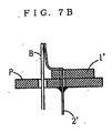
- Prior art is shown in fig. 7b of the present patent application. Documents reflecting this prior art are "Japanese Patent unexamined publication gazette Heisei 9-120853" and "Japanese Utility Model examined publication gazette Heisei 7-35313".
- Starting from such a prior art connector it is the object of the present invention to improve the reliability and enhance the workability of assembly of printed circuit boards.
- This object is achieved by the features of
claim 1. Especially, a pin-shaped conducting member is connected to the contact by soldering, after the pin-shaped conducting member has been guided in via the inlet hole. Especially, the arrangement of the connector ofclaim 1 has the advantage that dripping of a solder can be prevented. - The dependent claims 2 and 3 show advantageous further developments of the connector according to
claim 1. - The connector is to be connected to a pin-shaped conducting member of a counterpart, said connector comprising, a base housing to be arranged on a printed circuit board, a slide housing being supported in such a way that it can slide in relation to the base housing in a plane that crosses the longitudinal direction of the conducting member of the counterpart, and at least one contact spanning both said housings, being fixed to both said housings and being to be soldered on the printed circuit board, said slide housing having at least one inlet hole of which one end faces to and opens to said contact and of which the other end widens toward the end and opens to the conducting member of the counterpart.
- This connector that can absorb alignment error is mounted by soldering the contact on the base housing side onto the printed circuit board. When the conducting member of the counterpart is inserted into the inlet hole, the conducting member will come close to the contact. When both the conducting member and the contact are soldered or crimped together, the connection will be completed. In this process, even if the center of conducting member of the counterpart and the center of the inlet hole are not aligned with each other due to an alignment error, the conducting member of the counterpart will be received by the wide openings of the inlet hole, and when the conducting member advance in the inlet hole, the slide housing will be slid in relation to the base housing by the elastic deformation of the contact in a plane that crosses the longitudinal direction of the conducting member of the counterpart to absorb the alignment error. Thus the connector and the conducting member of the counterpart can be reliably connected with each other despite the existence of an alignment error. Furthermore, the stresses on the soldered parts, etc. are lessened in proportion to the flection of the contact. Hence troubles such as cracking due to excessive stresses caused in soldered parts by forceful connection can be avoided to prevent occurrence of defective connection. This can enhance the reliability of the connector. Moreover, as the conducting member of the counterpart is accepted by the inlet hole and received smoothly, the workability of assembly of printed circuit boards is improved. The above-mentioned desirable effects are particularly conspicuous when a large number of connectors and conducting members of counterpart are mounted and they are connected at a time to make a board-to-board connection.
- In the following, some embodiments of the present invention will be described with reference to the drawings.
- Fig. 1 is a perspective view of the first embodiment of the connector that absorbs alignment error.
- Fig. 2 is an exploded perspective view showing a base housing and a slide housing of the first embodiment of the connector that absorbs alignment error.
- Fig. 3 is a perspective view showing contacts being assembled on the slide housing of the first embodiment of the connector that absorbs alignment error.
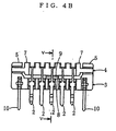
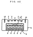
- Fig. 4A through Fig. 4C show the first embodiment of the connector that absorbs alignment error. Fig. 4A is a plan view, Fig. 4B is a front view, and Fig. 4C is a bottom view, respectively.
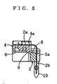
- Fig. 5 is a sectional view along the line V-V of Fig. 4B.
- Fig. 6 is a reduced perspective view showing a case and a printed circuit board that are to be connected with the first embodiment of the connector that absorbs alignment error.
- Fig. 7A and Fig. 7B are sectional views showing states of connection between a contact and a conducting member of the counterpart. Fig. 7A shows the case of the first embodiment of the connector that absorbs alignment error. Fig. 7B shows a case for comparison.
- Fig. 8 is an enlarged sectional view showing a relevant part of the second embodiment of the connector that absorbs alignment error.
- Fig. 9 is a perspective view of the third embodiment of the connector that absorbs alignment error.
-
- Fig. 1 through Fig. 5 show the first embodiment of the connector that absorbs alignment error. This connector that absorbs alignment error is mounted, for example as shown in Fig. 6, on a printed circuit board P when a case C and the printed circuit board P are connected with each other. In the example shown in Fig. 6, pin-shaped conducting members B of the counterpart are mounted in the case C in such a way that the conducting members B protrude upwards. The conducting members B of the counterpart are arranged to pass upward through and come out of through windows W opened in the printed circuit board P, and to be connected to the connectors that absorb alignment error (not illustrated in Fig. 6).
- As shown in Fig. 1 through Fig. 5, the connector of the first . embodiment comprises, a
housing 1 made of an insulating material andcontacts 2 that are made of an elastic conducting material, and thecontacts 2 are to be soldered on the printed circuit board B. The connector comprises, abase housing 3 to be arranged on a printed circuit board P, aslide housing 4 being supported in such a way that it can slide in relation to thebase housing 3 in a plane that crosses the longitudinal direction of the conducting member B of the counterpart, andcontacts 2 spanning both saidhousings housings base housing 3, clampingparts 5, being formed into a fallen-U-shape and opening forward are provided, one on the right and the other on the left, at a distance from each other. Theslide housing 4 is slidably held at theends 4b by theseclamping parts 5. - At least a part of each
contact 2 spans thebase housing 3 and theslide housing 4 and is fixed onto bothhousings contact 2 comprises a connectingpart 2a and a mountingpart 2b and is substantially formed into an inverted-L shape. The connectingpart 2a is fixed on the top of theslide housing 4. The mountingpart 2b spans both thehousings slide housing 4 and the front of thebase housing 3 to connect both thehousings contact 2 is fitted intogrooves base housing 3 and theslide housing 4, respectively. As shown in Fig. 1, abend 2c is formed on some or all of the mountingparts 2b of thecontacts 2 by bending the mountingpart 2b near its top end in the longitudinal direction. When these bends 2c are fitted in through holes made in the printed circuit board P, thebends 2c will undergo an elastic deformation and resulting restoring forces will tack the connector that absorbs alignment error on the printed circuit board P. Furthermore, as shown in Fig. 4A, a hole forimage recognition 2d is formed in the connectingpart 2a of eachcontact 2, and when the connectingpart 2a is automatically soldered to a conducting member B of the counterpart, the position of the part to be soldered will be recognized to make positional error correction of the automatic soldering machine. - The
slide housing 4 is provided withinlet holes 6 of which one end opens to and faces to thecontact 2 and of which the other end widens toward the end, opens to and faces to the conducting member B of the counterpart. The upper end of theinlet hole 6 directly leads to the top of the contact's connectingpart 2a on theslide housing 4, and the lower end of theinlet hole 6 opens in the bottom of theslide housing 4. - The
slide housing 4 to be held between the clampingparts 5 of the above-mentionedbase housing 3 is provided withlateral stoppers 7 that will touch and rest on theclamping parts 5, when theslide housing 4 shifts sidewise. Alongitudinal stopper 8 is protrusively provided on the top of thebase housing 3, and alongitudinal stopper 9 is protrusively provided on the bottom of theslide housing 4, respectively, and they will touch and rest on each other when theslide housing 4 shifts forward. When theslide housing 4 is fitted on thebase housing 3, one of thelongitudinal stoppers base housing 3. Such reinforcingtabs 10 are provided when necessary. This reinforcingtab 10 is inserted into a through hole in the printed circuit board P and soldered therein to increase the mounting strength of the connector that absorbs alignment error on the printed circuit board P. - The above-mentioned first embodiment of the connector that absorbs alignment error is mounted by, as shown in Fig. 7A, soldering the top end of the mounting
part 2b of eachcontact 2 onto the printed circuit board P. When a conducting member B of the counterpart is inserted into aninlet hole 6, the conducting member B of the counterpart will penetrate through the connectingpart 2a of thecontact 2. Connection is completed when both the conducting member B and the connectingpart 2a are soldered or crimped together. In the process, even if the center of the conducting member B of the counterpart and the center of theinlet hole 6 are not aligned with each other due to alignment error, the conducting member B of the counterpart will be caught by the wide opening of theinlet hole 6, and when the conducting member B of the counterpart advances in theinlet hole 6, theslide housing 4 will slide in relation to thebase housing 3 in a plane crossing the longitudinal direction of the conducting member B of the counterpart due to elastic deformation of thecontact 2. Hence the conducting member B of the counterpart will be guided to thecontact 2 and can be connected to it. Because alignment error can be absorbed as described above, connection failure of the connector and the conducting member B of the counterpart can be prevented effectively and the reliability of the connector is improved. Furthermore, as the stress on a soldered part, etc. is lessened in proportion to the flection of thecontact 2, troubles such as cracking in the soldered part can be avoided and defective connection can be prevented from occurring. Thus the reliability of the connector is enhanced. Moreover, as the conducting member B of the counterpart is caught by theinlet hole 6 and smoothly guided deep into theinlet hole 6, the workability of assembly of the printedcircuit board 6 is improved. The above-mentioned effects are particularly conspicuous when a large number of connectors and conducting members B of counterpart are mounted and they are connected collectively in a board-to-board connection. - In the above-mentioned first embodiment, when the connecting
part 2a is fixed on the top of theslide housing 4 and the top end of theinlet hole 6 directly leads to the top of the connectingpart 2a of thecontact 2 on theslide housing 4, the conducting member B of the counterpart that penetrates thecontact 2 can be soldered onto the top of thecontact 2 and no drip of solder will be generated. The good effect of this arrangement is obvious when it is compared with a case wherein, as shown in Fig. 7B, a contact 2' is fitted on a single housing 1' and the top end of the contact 2' is put against the conducting member B of the counterpart and soldered. - Further, the present invention includes embodiments wherein the
lateral stoppers 7, and thelongitudinal stoppers stoppers slide housing 4 is restrained by thelateral stoppers 7, forward shift of theslide housing 4 is restrained by thelongitudinal stoppers ends 4b of theslide housing 4 are held by the clampingparts 5 of the base housing and backward shift of theslide housing 4 is restrained by them. As these restraints set the limits of its movable range, excessive deformation of thecontact 2 is prevented and troubles such as damages are prevented to improve the reliability of the connector. - In the above-mentioned case for comparison shown in Fig. 7B, as the contact 2' protrudes bare, when the connector is mounted on a printed circuit board P and when the contact 2' is connected to a conducting member B of the counterpart, the contact 2' may hit on another member, etc. to cause a trouble, such as bending or breakage of the contact 2'. In contrast to this, in the above-mentioned first embodiment, as the connecting
part 2a of thecontact 2 is fixed to theslide housing 4 and the mountingpart 2b is fixed to theslide housing 4 and thebase housing 3, such a trouble does not occur; failure in connection between the connector and the conducting member B of the counterpart can be effectively prevented from occurring. Moreover, the present invention includes embodiments wherein contacts are directly fixed on the surface of the housing. However, as is the case in the above-mentioned first embodiment, whengrooves housings contact 2 is fitted in thesegrooves contact 2 will be protected by thegrooves contact 2 and the conducting member B of the counterpart is more effectively prevented and the reliability of the connector is improved. - In the above-mentioned first embodiment, when the mounting
part 2b of thecontact 2 is provided with abend 2c, the connector that absorbs alignment error can be tacked to the printed circuit board P and the assembly can be brought to the next step by just insertingcontacts 2 in the printed circuit board P. This eliminates a conventional step of bending the top ends of contacts that are inserted in the printed circuit board P to prevent the connector from coming off from the printed circuit board P. As a result, the efficiency of mass production is improved. - The present invention includes embodiments wherein the connecting
part 2a of thecontact 2 is not provided with a hole forimage recognition 2d. However; as is the case in the above-mentioned first embodiment, when the hole forimage recognition 2d is formed, positional error correction can be made by an automatic soldering machine. This improves the accuracy of soldering and improves the yield of the products. - Fig. 8 shows the second embodiment. Only differences in structure of this second embodiment from the above-mentioned first embodiment will be described. A
small protrusion 11 is formed on the bottom of the clampingpart 5 of thebase housing 3, and adent 12 into which theprotrusion 11 fits is concavely formed on the top of theslide housing 4, and during assembly theslide housing 4 can be tacked to thebase housing 3. With this arrangement, when, for example, theslide housing 4 is tentatively fixed in the regular position in relation to thebase housing 3 and thebase housing 3 is mounted on the printed circuit board, the probability of eachinlet hole 6 catching the conducting member B of the counterpart will increase and, in turn, the function of absorbing alignment error will be enhanced. - Fig. 9 shows the third embodiment. Only differences in structure of this third embodiment from the above-mentioned first embodiment will be described. The top end of the connecting
part 2a of thecontact 2 is raised at both ends in the width direction to have a substantially-U-shaped section. A portion of theslide housing 4 between the above-mentioned U-shaped parts of twoadjacent contacts 2, which is exposed to the effects of soldering, is partly cut away at the top to form areduced part 4c which is lower in height than other portions. This eliminates portions of theslide housing 4 that might be scorched when soldering is made automatically by laser beam or the like, and in turn improves the reliability of the product and improves the yield. - The above-mentioned embodiments are just examples and the present invention is not limited by them. The connector that absorbs alignment error according to the present invention can be used extensively as a connector to be mounted on a printed circuit board, case, etc.
- In the present invention, the number of the clamping parts is not limited to two, and clamping parts may be provided at three points or more. The clamping parts may be arranged to open at sides or at the rear. In such a case, when a stopper or stoppers is provided in response to this arrangement, the stopper or stoppers is provided in such a way that the slide housing does not shift towards the opening of the clamping parts.
- The present invention includes other embodiments wherein the slide housing is supported in such a way that it can slide in relation to the base housing in a plane crossing the longitudinal direction of conducting member of the counterpart. For example, in one of such embodiments, a pillar is erected on the top of the base housing, this pillar is made to penetrate through the slide housing, and the gap between the pillar and the slide housing is set large.
- In the above-mentioned embodiments, the contact is divided into the connecting part and the mounting part, and the mounting part spans both the housings and fixed on the front of the slide housing and the front of the base housing. The present invention, however, includes embodiments wherein another part of the contact spans both the housings and fixed to both the housings.
- One end of the inlet hole faces to and opens to the above-mentioned contact. This means that the one end of the inlet hole opens near the contact. In a further embodiment of the present invention one end of the inlet hole opens near an edge of the contact. In a further embodiment of the present invention the inlet hole ends at the top of the slide housing and does not penetrate through and reach the top of the contact.
- Also the present invention includes the embodiment wherein the number of the contact is one, the embodiments wherein the number of the contacts is two or more.
Claims (3)
- A connector to be connected to a pin-shaped conducting member (B), said connector comprising:a base housing (3) having a bottom surface, a top surface and side surfaces, said bottom surface being arrangable on a printed circuit board (P), at least one contact (2) being fixed to one of said side surfaces of said base housing (3) and being to be soldered on said printed circuit board (P), characterized in thata slide housing (4) being arranged on and supported by said base housing (3) in such a way that it can slide in relation to said base housing (3) in a plane that crosses the longitudinal direction of said pin-shaped conducting member (B), andat least one contact (2) spanning said side surface of said base housing (3) and a top surface of said slide housing (4), being fixed thereto,said slide housing (4) having at least one inlet hole (6), wherein the end at a bottom surface of said slide housing (4) of said inlet hole (6) widens for receiving an end portion of said pin-shaped conducting member (B) to be guided through said inlet hole (6) to said contact (2) and to be soldered with said contact (2) at the top surface of said slide housing (4).
- Connector according to claim 1, wherein
said base housing (3) has two clamping parts (5), being arranged on the top surface at the outer ends in a longitudinal direction thereof, respectively, said clamping parts (5) being formed into a fallen-U-shape and opening in a lateral direction of said base housing (3) for receiving and slidably holding said slide housing (4),
said contact (2) has a connecting part (2a) and a mounting part (2b), said contact being formed into a substantially inverted L-shape, said connecting part (2a) being fixed on the top surface of said slide housing (4) and said mounting part (2b) spanning both the housings (3, 4) and being fixed to the top surface of said slide housing (4), continued to said connecting part (2a) and fixed to said one of said side surfaces, being the front surface, of said base housing (3), and
said inlet hole (6) coming from said slide housing (4) continues through said connecting part (2a) of said contact (2), wherein said pin-shaped conducting member (B) guided through said inlet hole (6) from the widened end thereof is guided through said slide housing (4) and said connecting part (2a) before the end portion of pin-shaped conducting member (B) is soldered with said connecting part (2a). - Connector according to claim 2, wherein
said slide housing (4) to be held between said clamping parts (5) of said base housing (3) has lateral stoppers (7) that will touch and rest on said clamping parts (5) when said slide housing (4) shifts in the longitudinal direction of said base housing (3), and
said base housing (3) has a longitudinal stopper (8) on the top surface thereof for touching and resting on a longitudinal stopper (9) of said slide housing (4) when said slide housing (4) shifts in the lateral direction of said base housing (3).
Applications Claiming Priority (2)
| Application Number | Priority Date | Filing Date | Title |
|---|---|---|---|
| JP37687398 | 1998-12-24 | ||
| JP37687398A JP4091702B2 (en) | 1998-12-24 | 1998-12-24 | Error absorbing connector |
Publications (2)
| Publication Number | Publication Date |
|---|---|
| EP1014509A1 EP1014509A1 (en) | 2000-06-28 |
| EP1014509B1 true EP1014509B1 (en) | 2003-04-02 |
Family
ID=18507876
Family Applications (1)
| Application Number | Title | Priority Date | Filing Date |
|---|---|---|---|
| EP99125449A Expired - Lifetime EP1014509B1 (en) | 1998-12-24 | 1999-12-20 | Conncetor that absorbs alignment error |
Country Status (8)
| Country | Link |
|---|---|
| US (1) | US6561829B2 (en) |
| EP (1) | EP1014509B1 (en) |
| JP (1) | JP4091702B2 (en) |
| KR (1) | KR100629745B1 (en) |
| CN (1) | CN1127784C (en) |
| DE (1) | DE69906464T2 (en) |
| HK (1) | HK1029668A1 (en) |
| TW (1) | TW437123B (en) |
Families Citing this family (15)
| Publication number | Priority date | Publication date | Assignee | Title |
|---|---|---|---|---|
| JP4056301B2 (en) * | 2002-06-11 | 2008-03-05 | 株式会社東海理化電機製作所 | Connector and connector mounting structure |
| TW568458U (en) * | 2003-05-23 | 2003-12-21 | Hon Hai Prec Ind Co Ltd | Electrical connector |
| US6908326B2 (en) * | 2003-08-08 | 2005-06-21 | J. S. T. Mfg. Co., Ltd. | Floating connector |
| TWM254745U (en) * | 2004-03-17 | 2005-01-01 | Benq Corp | Connector |
| JP4258466B2 (en) * | 2004-12-16 | 2009-04-30 | セイコーエプソン株式会社 | Piezoelectric gyro element and piezoelectric gyroscope |
| CN2766391Y (en) * | 2004-12-20 | 2006-03-22 | 富士康(昆山)电脑接插件有限公司 | Electric connector |
| DE102006039415B4 (en) * | 2006-08-23 | 2008-05-15 | Siemens Ag | Contact strip, contact device and method for producing a printed circuit board |
| US7473133B1 (en) * | 2007-07-05 | 2009-01-06 | Hon Hai Precision Ind. Co., Ltd. | Electrical connector |
| JP5316334B2 (en) * | 2009-09-16 | 2013-10-16 | 富士通株式会社 | Electronic component manufacturing apparatus and manufacturing method |
| JP5587807B2 (en) * | 2011-02-07 | 2014-09-10 | ケル株式会社 | Floating connector |
| CN103547137B (en) | 2012-07-09 | 2016-04-27 | 鸿富锦精密工业(深圳)有限公司 | Stitch means for correcting and correcting structure thereof |
| DE102014114352B3 (en) * | 2014-10-02 | 2016-03-10 | Wago Verwaltungsgesellschaft Mbh | pin header |
| JP6567852B2 (en) * | 2015-03-26 | 2019-08-28 | 京セラ株式会社 | Floating connector device |
| DE102017112025B4 (en) * | 2017-06-01 | 2019-09-12 | Ims Connector Systems Gmbh | Electrical connector with tolerance compensation |
| EP3471520B1 (en) | 2017-10-10 | 2021-10-06 | Vitesco Technologies GmbH | Printed circuit board mounting arrangement |
Family Cites Families (10)
| Publication number | Priority date | Publication date | Assignee | Title |
|---|---|---|---|---|
| FR2639481B1 (en) * | 1988-11-21 | 1991-03-15 | Peugeot | DEVICE FORMING ELECTRICAL CONNECTOR |
| JPH087171B2 (en) | 1989-06-07 | 1996-01-29 | 日本碍子株式会社 | Gas analyzer calibration method and gas concentration measuring device |
| IT1248178B (en) | 1991-06-18 | 1995-01-05 | Microstamp Srl | BREAKER DEVICE |
| JP3016164B2 (en) * | 1991-06-19 | 2000-03-06 | 日本エー・エム・ピー株式会社 | Movable connector |
| JPH06111865A (en) * | 1992-08-06 | 1994-04-22 | Du Pont Singapore Pte Ltd | Face-mounting connector device |
| US5453016A (en) * | 1993-11-15 | 1995-09-26 | Berg Technology, Inc. | Right angle electrical connector and insertion tool therefor |
| JP2937728B2 (en) * | 1993-12-13 | 1999-08-23 | 日本圧着端子製造 株式会社 | Printed wiring board connector |
| JP3106957B2 (en) * | 1996-05-27 | 2000-11-06 | 住友電装株式会社 | Board connector |
| JPH09320706A (en) * | 1996-05-28 | 1997-12-12 | Yazaki Corp | Printed circuit board connector |
| US6095826A (en) * | 1997-02-21 | 2000-08-01 | Berg Technology, Inc. | Press fit circuit board connector |
-
1998
- 1998-12-24 JP JP37687398A patent/JP4091702B2/en not_active Expired - Lifetime
-
1999
- 1999-12-17 TW TW088122297A patent/TW437123B/en not_active IP Right Cessation
- 1999-12-20 EP EP99125449A patent/EP1014509B1/en not_active Expired - Lifetime
- 1999-12-20 DE DE69906464T patent/DE69906464T2/en not_active Expired - Lifetime
- 1999-12-21 US US09/468,321 patent/US6561829B2/en not_active Expired - Fee Related
- 1999-12-22 KR KR1019990060132A patent/KR100629745B1/en not_active IP Right Cessation
- 1999-12-23 CN CN99127414A patent/CN1127784C/en not_active Expired - Fee Related
-
2001
- 2001-01-17 HK HK01100435A patent/HK1029668A1/en not_active IP Right Cessation
Also Published As
| Publication number | Publication date |
|---|---|
| CN1260608A (en) | 2000-07-19 |
| CN1127784C (en) | 2003-11-12 |
| HK1029668A1 (en) | 2001-04-06 |
| DE69906464T2 (en) | 2004-01-15 |
| US20020111075A1 (en) | 2002-08-15 |
| US6561829B2 (en) | 2003-05-13 |
| KR20000048316A (en) | 2000-07-25 |
| EP1014509A1 (en) | 2000-06-28 |
| DE69906464D1 (en) | 2003-05-08 |
| JP2000195615A (en) | 2000-07-14 |
| JP4091702B2 (en) | 2008-05-28 |
| KR100629745B1 (en) | 2006-09-28 |
| TW437123B (en) | 2001-05-28 |
Similar Documents
| Publication | Publication Date | Title |
|---|---|---|
| EP1014509B1 (en) | Conncetor that absorbs alignment error | |
| US6902411B2 (en) | Connector assembly | |
| US6033245A (en) | Self-aligning electrical connector | |
| KR101450401B1 (en) | Electric connector | |
| CN110932006B (en) | Electric connector and manufacturing method thereof | |
| KR100383374B1 (en) | Coaxial connector with switch and method for manufacturing the same | |
| US8021187B2 (en) | Electric connector | |
| US6884108B2 (en) | Connector for flexible printed circuit | |
| KR100344048B1 (en) | Inspectable electrical connector for pga package | |
| US20120329319A1 (en) | Bending Coaxial Electrical Connector | |
| EP0559057B1 (en) | Electrical connector terminal | |
| EP0996993B1 (en) | Latched and shielded electrical connectors | |
| CN110247213B (en) | Intermediate electric connector and electric connector assembly | |
| JP2000195615A5 (en) | ||
| CN216085565U (en) | Electrical connector | |
| US20230387633A1 (en) | Shield connector | |
| JP2767537B2 (en) | Movable electrical connector | |
| US7056133B2 (en) | Surface mounting connector | |
| EP1116956B1 (en) | Electrical continuity inspection unit for connector | |
| KR20040098568A (en) | A connector and connector assembly | |
| CN110718791B (en) | Electrical connector | |
| CN111082244B (en) | Connector with a plurality of connectors | |
| CN112117569A (en) | Electric connector and manufacturing method thereof | |
| US20030032329A1 (en) | Connector for printed circuit board | |
| JP2003022851A (en) | Connector |
Legal Events
| Date | Code | Title | Description |
|---|---|---|---|
| PUAI | Public reference made under article 153(3) epc to a published international application that has entered the european phase |
Free format text: ORIGINAL CODE: 0009012 |
|
| AK | Designated contracting states |
Kind code of ref document: A1 Designated state(s): DE FR GB |
|
| AX | Request for extension of the european patent |
Free format text: AL;LT;LV;MK;RO;SI |
|
| RIN1 | Information on inventor provided before grant (corrected) |
Inventor name: JUNICHI ITOH, C/O J.S.T. MFG. CO., LTD., Inventor name: NINOMIYA, NORIHIRO, C/OTOYOTA JIDOSHA K.K., Inventor name: MAEDA, TOMOHARU, C/OTOYOTA JIDOSHA K.K., |
|
| 17P | Request for examination filed |
Effective date: 20001108 |
|
| 17Q | First examination report despatched |
Effective date: 20010130 |
|
| AKX | Designation fees paid |
Free format text: DE FR GB |
|
| GRAG | Despatch of communication of intention to grant |
Free format text: ORIGINAL CODE: EPIDOS AGRA |
|
| GRAG | Despatch of communication of intention to grant |
Free format text: ORIGINAL CODE: EPIDOS AGRA |
|
| GRAH | Despatch of communication of intention to grant a patent |
Free format text: ORIGINAL CODE: EPIDOS IGRA |
|
| GRAH | Despatch of communication of intention to grant a patent |
Free format text: ORIGINAL CODE: EPIDOS IGRA |
|
| GRAA | (expected) grant |
Free format text: ORIGINAL CODE: 0009210 |
|
| AK | Designated contracting states |
Designated state(s): DE FR GB |
|
| REG | Reference to a national code |
Ref country code: GB Ref legal event code: FG4D |
|
| REF | Corresponds to: |
Ref document number: 69906464 Country of ref document: DE Date of ref document: 20030508 Kind code of ref document: P |
|
| ET | Fr: translation filed | ||
| PLBE | No opposition filed within time limit |
Free format text: ORIGINAL CODE: 0009261 |
|
| STAA | Information on the status of an ep patent application or granted ep patent |
Free format text: STATUS: NO OPPOSITION FILED WITHIN TIME LIMIT |
|
| 26N | No opposition filed |
Effective date: 20040105 |
|
| REG | Reference to a national code |
Ref country code: FR Ref legal event code: PLFP Year of fee payment: 17 |
|
| REG | Reference to a national code |
Ref country code: FR Ref legal event code: PLFP Year of fee payment: 18 |
|
| REG | Reference to a national code |
Ref country code: FR Ref legal event code: PLFP Year of fee payment: 19 |
|
| PGFP | Annual fee paid to national office [announced via postgrant information from national office to epo] |
Ref country code: DE Payment date: 20171211 Year of fee payment: 19 Ref country code: FR Payment date: 20171221 Year of fee payment: 19 |
|
| PGFP | Annual fee paid to national office [announced via postgrant information from national office to epo] |
Ref country code: GB Payment date: 20171221 Year of fee payment: 19 |
|
| REG | Reference to a national code |
Ref country code: DE Ref legal event code: R119 Ref document number: 69906464 Country of ref document: DE |
|
| GBPC | Gb: european patent ceased through non-payment of renewal fee |
Effective date: 20181220 |
|
| PG25 | Lapsed in a contracting state [announced via postgrant information from national office to epo] |
Ref country code: FR Free format text: LAPSE BECAUSE OF NON-PAYMENT OF DUE FEES Effective date: 20181231 Ref country code: DE Free format text: LAPSE BECAUSE OF NON-PAYMENT OF DUE FEES Effective date: 20190702 |
|
| PG25 | Lapsed in a contracting state [announced via postgrant information from national office to epo] |
Ref country code: GB Free format text: LAPSE BECAUSE OF NON-PAYMENT OF DUE FEES Effective date: 20181220 |