JP4088742B2 - Photomask blank, photomask, and method for manufacturing photomask blank - Google Patents
Photomask blank, photomask, and method for manufacturing photomask blank Download PDFInfo
- Publication number
- JP4088742B2 JP4088742B2 JP2000396138A JP2000396138A JP4088742B2 JP 4088742 B2 JP4088742 B2 JP 4088742B2 JP 2000396138 A JP2000396138 A JP 2000396138A JP 2000396138 A JP2000396138 A JP 2000396138A JP 4088742 B2 JP4088742 B2 JP 4088742B2
- Authority
- JP
- Japan
- Prior art keywords
- film
- chromium
- photomask
- seed layer
- photomask blank
- Prior art date
- Legal status (The legal status is an assumption and is not a legal conclusion. Google has not performed a legal analysis and makes no representation as to the accuracy of the status listed.)
- Expired - Lifetime
Links
Images


Classifications
-
- G—PHYSICS
- G03—PHOTOGRAPHY; CINEMATOGRAPHY; ANALOGOUS TECHNIQUES USING WAVES OTHER THAN OPTICAL WAVES; ELECTROGRAPHY; HOLOGRAPHY
- G03F—PHOTOMECHANICAL PRODUCTION OF TEXTURED OR PATTERNED SURFACES, e.g. FOR PRINTING, FOR PROCESSING OF SEMICONDUCTOR DEVICES; MATERIALS THEREFOR; ORIGINALS THEREFOR; APPARATUS SPECIALLY ADAPTED THEREFOR
- G03F1/00—Originals for photomechanical production of textured or patterned surfaces, e.g., masks, photo-masks, reticles; Mask blanks or pellicles therefor; Containers specially adapted therefor; Preparation thereof
- G03F1/38—Masks having auxiliary features, e.g. special coatings or marks for alignment or testing; Preparation thereof
- G03F1/46—Antireflective coatings
-
- G—PHYSICS
- G03—PHOTOGRAPHY; CINEMATOGRAPHY; ANALOGOUS TECHNIQUES USING WAVES OTHER THAN OPTICAL WAVES; ELECTROGRAPHY; HOLOGRAPHY
- G03F—PHOTOMECHANICAL PRODUCTION OF TEXTURED OR PATTERNED SURFACES, e.g. FOR PRINTING, FOR PROCESSING OF SEMICONDUCTOR DEVICES; MATERIALS THEREFOR; ORIGINALS THEREFOR; APPARATUS SPECIALLY ADAPTED THEREFOR
- G03F1/00—Originals for photomechanical production of textured or patterned surfaces, e.g., masks, photo-masks, reticles; Mask blanks or pellicles therefor; Containers specially adapted therefor; Preparation thereof
- G03F1/50—Mask blanks not covered by G03F1/20 - G03F1/34; Preparation thereof
-
- G—PHYSICS
- G03—PHOTOGRAPHY; CINEMATOGRAPHY; ANALOGOUS TECHNIQUES USING WAVES OTHER THAN OPTICAL WAVES; ELECTROGRAPHY; HOLOGRAPHY
- G03F—PHOTOMECHANICAL PRODUCTION OF TEXTURED OR PATTERNED SURFACES, e.g. FOR PRINTING, FOR PROCESSING OF SEMICONDUCTOR DEVICES; MATERIALS THEREFOR; ORIGINALS THEREFOR; APPARATUS SPECIALLY ADAPTED THEREFOR
- G03F1/00—Originals for photomechanical production of textured or patterned surfaces, e.g., masks, photo-masks, reticles; Mask blanks or pellicles therefor; Containers specially adapted therefor; Preparation thereof
- G03F1/38—Masks having auxiliary features, e.g. special coatings or marks for alignment or testing; Preparation thereof
Landscapes
- Physics & Mathematics (AREA)
- General Physics & Mathematics (AREA)
- Preparing Plates And Mask In Photomechanical Process (AREA)
- Exposure And Positioning Against Photoresist Photosensitive Materials (AREA)
Description
【0001】
【発明の属する技術分野】
本発明は、半導体集積回路及び高密度集積回路等の製造工程において使用されるフォトマスクブランクス、フォトマスク及びフォトマスクブランクスの製造方法に関する。
【0002】
【従来の技術】
LSI、VLSI等の高密度半導体集積回路、CCD(電荷結合素子)やLCD(液晶表示素子)用のカラーフィルター、磁気ヘッド等の微細加工には、フォトマスクを使ったフォトリソグラフィー技術が用いられている。
【0003】
この微細加工には、石英ガラス、アルミノシリケートガラス等の透明な基板の上に一般的にはクロム膜からなる遮光膜をスパッタ又は真空蒸着等で形成したフォトマスクブランクスを用いて、この遮光膜に所定のパターンを形成したものをフォトマスクとして用いている。
【0004】
この場合、クロム系の遮光膜は光反射率が大きく、被露光物である半導体基板で反射した光が投影レンズを通ってフォトマスクで反射し、再び半導体基板に戻ることを防止するため、遮光膜の表面、表面及び裏面に反射防止膜を通常形成している。
【0005】
このようなフォトマスクに使用されるマスクブランクスの構造として、合成石英基板上に遮光膜をスパッタもしくは真空蒸着等で形成し、さらに遮光膜として用いるクロム膜の表層部には、シリコンウェハから反射した露光光が再度反射されるのを防止する反射防止膜を設けているもの(2層構造膜)や、基板側にも反射防止膜を設けるもの(3層構造膜)等があり、従来、基板側の反射防止膜としてクロム炭化物及びクロム窒化物を含有するクロム炭化窒化物膜を、遮光膜としてクロム膜を、表面側の反射防止膜としてクロム酸化物及びクロム窒化物を含有するクロム酸化窒化物膜を順次積層したフォトマスクブランクスが提案されている(特公昭62−37385号公報)。さらに、反射防止膜としてCrONを用いたもの(特公昭61−46821号公報、特公昭62−27387号公報)、CrNを用いたもの(特公昭62−27386号公報、特公昭62−27387号公報)等が提案されている。また、窒化クロムを用いた単層膜(特公平4−1339号公報)等も提案されている。
【0006】
しかし、高密度半導体集積回路の微細化、高集積化にともない、フォトマスクブランクスの欠陥検査や回路パターン検査において、検出感度の高い検査が行われるようになり、遮光膜及び反射防止膜はより高い膜質の均一性が求められている。
【0007】
【発明が解決しようとする課題】
ところで、フォトマスクはパターンを正確に転写するためには、基板が平坦であることが強く要求されるが、いかに平坦な基板を用いても、クロム系膜を形成すると、特に2層構造の膜では遮光膜が基板表面で大きな粒状に成長する特徴があるため、表面の状態は悪くなる傾向がある。現在の欠陥検査及び回路パターン検査では、反射光及び透過光による検査が一般的であるが、高検出感度の検査では、膜表面の状態、面荒れを欠陥として検出する場合があるので、高感度の検査が行えない等の問題点がある。
【0008】
本発明は、上記問題点を鑑みなされたもので、膜質の均一性が得られ、欠陥検査及び回路パターン検査においても高感度検出が可能となり、所望とする微細なパターンを歪みなく正確に形成することが可能な高性能なフォトマスクブランクス及びフォトマスクを提供することを目的とする。
【0009】
【課題を解決するための手段及び発明の実施の形態】
本発明者は、上記目的を達成するため鋭意検討を重ねた結果、透明基板上に少なくとも一層の遮光膜と少なくとも一層の反射防止膜とを有するフォトマスクブランクス及びフォトマスクにおいて、透明基板と遮光膜又は反射防止膜との間に、シード層を、クロム酸化窒化物、クロム酸化炭化物又はクロム酸化窒化炭化物からなる材料で、厚さを0.5〜5nmとして形成することによって、遮光膜又は反射防止膜の表面平坦度が高く、均一な膜質のフォトマスクブランクス及びフォトマスクが得られることを知見し、本発明をなすに至った。
【0010】
即ち、本発明は、下記のフォトマスクブランクス、フォトマスク及びフォトマスクブランクスの製造方法を提供する。
請求項1:
露光光が透過する透明基板上に少なくとも一層の遮光膜と少なくとも一層の反射防止膜を有するフォトマスクブランクスにおいて、上記透明基板と遮光膜又は反射防止膜との間にシード層を形成すると共に、このシード層をクロム酸化窒化物、クロム酸化炭化物又はクロム酸化窒化炭化物からなる材料で、厚さを0.5〜5nmとして形成したことを特徴とするフォトマスクブランクス。
請求項2:
上記遮光膜又は反射防止膜を酸素、窒素及び炭素の少なくとも1種を含むクロムからなる材料で形成したことを特徴とする請求項1に記載のフォトマスクブランクス。
請求項3:
上記フォトマスクブランクスの表面粗度(RMS)を0.9nm以下とする請求項2に記載のフォトマスクブランクス。
請求項4:
上記シード層を反応性スパッタにより形成したことを特徴とする請求項1乃至3のいずれか1項に記載のフォトマスクブランクス。
請求項5:
請求項1乃至4のいずれか1項に記載のフォトマスクブランクスをリソグラフィ法によりパターン形成してなることを特徴とするフォトマスク。
請求項6:
露光光が透過する透明基板上に少なくとも一層の遮光膜と少なくとも一層の反射防止膜を有するフォトマスクブランクスを製造する方法であって、上記透明基板と遮光膜又は反射防止膜との間に、クロム酸化窒化物、クロム酸化炭化物又はクロム酸化窒化炭化物からなる材料で、厚さ0.5〜5nmのシード層を形成し、該シード層上に上記遮光膜又は反射防止膜を形成することを特徴とするフォトマスクブランクスの製造方法。
請求項7:
上記遮光膜又は反射防止膜を酸素、窒素及び炭素の少なくとも1種を含むクロムからなる材料で形成することを特徴とする請求項6に記載のフォトマスクブランクスの製造方法。
請求項8:
上記シード層を反応性スパッタにより形成することを特徴とする請求項6又は7に記載のフォトマスクブランクスの製造方法。
【0011】
本発明のシード層を持ったマスクブランクス及びフォトマスクによれば、透明基板上のシード層が、遮光膜又は反射防止膜の成長核となり、シード層の上の遮光膜及び反射防止膜の成長が微細な粒状成長になり、結果として表面粗度の小さいフォトマスクブランクス及びフォトマスクを得ることができる。
【0012】
以下、本発明につき更に詳しく説明する。
本発明のフォトマスクブランクスは、図1,3に示したように、露光光が透過する透明基板1上に少なくとも一層の遮光膜2と少なくとも一層の反射防止膜4を有し、上記透明基板1と遮光膜2または反射防止膜4との間にシード層3を形成すると共に、このシード層3が酸素、窒素及び炭素の少なくとも1種を含むクロムからなる材料で形成したことを特徴とし、これにより、フォトマスクブランクスの表面平坦度が向上するものである。
【0013】
この場合、図1に示したように、シード層の上に遮光膜が一層、反射防止膜が一層の3層構造の場合、基板上にシード層、このシード層の上に遮光膜、さらに遮光膜の上に反射防止膜を順次形成することが好ましい。
【0014】
また、図3に示したように、シード層の上に遮光膜が一層、反射防止膜が二層の4層構造のフォトマスクブランクスの場合、基板上にシード層、このシード層の上に第1の反射防止膜、この第1の反射防止膜の上に遮光膜、さらに遮光膜の上に第2の反射防止膜を順次形成することが好ましい。
【0015】
ここで、成膜に用いる基板としては特に制限されず、例えば、石英、アルミノシリケートガラス、フッ化カルシウム、フッ化マグネシウム等が好ましい。
【0016】
本発明においては、この基板上にシード層を形成する。上記シード層としては、酸素、窒素、炭素を少なくとも1種含むクロムからなる材料が好適であり、例えば、クロム酸化物、クロム窒化物、クロム酸化窒化物、クロム酸化炭化物、クロム酸化窒化炭化物等が挙げられるが、特にクロム酸化炭化物、クロム酸化窒化炭化物が好ましい。
【0017】
この場合、シード層中のクロム量は、25〜60原子%、特に30〜50原子%とすることが好ましい。クロム酸化窒化物の場合、窒素量は2〜50原子%、特に10〜30原子%、酸素量は5〜60原子%、特に20〜50原子%が好ましく、クロム酸化炭化物の場合、炭素量は2〜50原子%、特に5〜25原子%、酸素量は5〜60原子%、特に20〜50原子%が好ましい。また、クロム炭化窒化酸化物の場合、窒素量は2〜50原子%、特に5〜25原子%、炭素量2〜50原子%、特に5〜25原子%、酸素量は5〜60原子%、特に20〜50原子%が好ましい。
【0018】
上記シード層の膜厚としては、初期の成長核となりうる必要最小限の厚さ0.5nm〜10nmであることが好ましい。より好ましくは0.5nm〜5nmである。膜厚が0.5nm未満であると表面粗度への改善効果がなく、10nmより厚くても改善効果は変わらず、かえって成膜時間が長くなり、生産性が低下する場合が生じる。
【0019】
このシード層の成膜方法はターゲットとしてクロムを用いた反応性スパッタ法により、基板側上に形成できるものである。
【0020】
スパッタ法としては、直流(DC)電源を用いたものでも、高周波(RF)電源を用いたものでもよく、またマグネトロンスパッタリング方式であっても、コンベンショナル方式であってもよいが、DCスパッタの方が機構が単純である点で好ましい。また、マグネトロンを用いた方が成膜速度が速くなり、生産性が向上する点から好ましい。なお、成膜装置は通過型でも枚葉型でも構わない。
【0021】
具体的には、シード層としてクロム酸化炭化物(CrCO)膜を成膜する場合、スパッタガスとしてCH4、CO2、CO等の炭素を含むガスと、CO2、O2等の酸素を含むガスそれぞれ1種以上を導入するか、これらにAr、Ne、Kr等の不活性ガスを混合したガスを用いることができる。特にスパッタガスとしてCO2又はCO2と不活性ガスとの混合ガスを用いると安全であり、CO2ガスは酸素等より反応性が低いが故に、チャンバ内の広範囲に均一にガスが回り込むことができ、成膜されるCrCO膜の膜質が均一になる点から好ましい。導入方法としては別々にチャンバ内に導入してもよい。
【0022】
シード層としてクロム酸化窒化炭化物(CrCON)膜を成膜する場合、スパッタガスとしてCH4、CO2、CO等の炭素を含むガスと、CO2、O2等の酸素を含むガスと、N2、NO等の窒素を含むガスのそれぞれ1種以上を導入するか、これらにAr、Ne、Kr等の不活性ガスを混合したガスを用いることができる。特にスパッタガスとしてCO2とN2又はCO2とN2と不活性ガスとの混合ガスを用いると安全であり、CO2ガスは酸素等より反応性が低いが故に、チャンバ内の広範囲に均一にガスが回り込むことができ、成膜されるCrCON膜の膜質が均一になる点から好ましい。導入方法としては別々にチャンバ内に導入してもよい。
【0023】
ターゲットとしてはクロム単体だけでなくクロムが主成分であるものであればよく、酸素、窒素、炭素のいずれかを含むクロム、又は酸素、窒素、炭素を組み合わせたものをクロムに添加したターゲットを用いてよい。
【0024】
なお、上記のようにシード層を形成する場合、低圧、高パワーでのスパッタが望ましい。低圧、高パワーの条件下では、スパッタ粒子のエネルギーが大きくなり、基板に対し斜めに入射するスパッタリング粒子が減少する。このため射影効果が抑制され、表面粗度の小さいシード層の成膜ができる。この場合、圧力は0.1〜1.0Pa、特に0.25〜0.32Paとすることがよく、パワーは3.9〜11.0w/cm2、特に7.0〜9.0w/cm2とすることがよい。
【0025】
また、上記遮光膜及び反射防止膜としては、酸素、窒素、炭素の少なくとも1種を含むクロム系材料が好適であり、例えば、クロム酸化物、クロム窒化物、クロム酸化窒化物、クロム酸化炭化物、クロム酸化窒化炭化物等が挙げられるが、特にクロム酸化炭化物、クロム酸化窒化炭化物が好ましい。これらの組成としては、公知の組成とすることができる。
【0026】
更に、遮光膜の厚さは10〜150nm、特に50〜80nmであることが好ましく、反射防止膜の厚さは10〜100nm、特に20〜40nmとすることが好ましい。
【0027】
なお、本発明のフォトマスクブランクスの膜構成としてはシード層の上にCr系の2層膜又は3層膜だけでなく、4層膜構造とすることもできる。更に露光波長の位相を変化させる位相シフター膜を組み合わせてもよい。また、透過型だけではなく、反射型マスクにも適応することができる。
【0028】
さらに、このようにシード層、遮光膜及び遮光膜を積層されたフォトマスクブランクスの表面粗度(RMS)を0.9nm以下にすることが好ましい。より好ましくは0.7nm以下である。この表面粗度は、シード層を上述したように形成することで達成し得る。
【0029】
このようにして得られる本発明のフォトマスクブランクスをリソグラフィ法によりパターン形成することにより、図2,4に示したようなシード層と遮光膜と反射防止膜とからなる3層,4層構造のフォトマスクが得られる。
【0030】
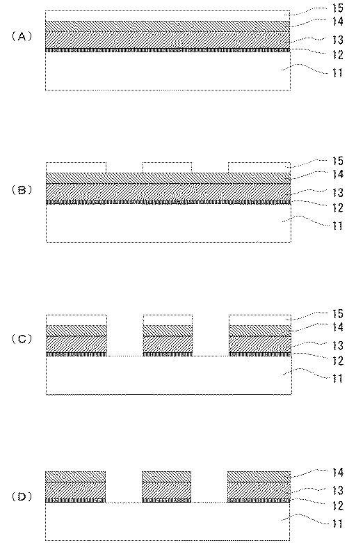
具体的には、本発明のフォトマスクブランクスを用いて図2に示したようなフォトマスクを製造する場合は、図5(A)に示したように、透明基板11の上にシード層12、その上に遮光膜13、遮光膜13の上に反射防止膜14を順次形成した後、反射防止膜14の上にレジスト膜15を形成し、図5(B)に示したように、レジスト膜15をパターニングし、更に、図5(C)に示したように、シード層12、遮光膜13及び反射防止膜14をドライエッチング又はウェットエッチングした後、図5(D)に示したように、レジスト膜15を剥離する方法が採用され得る。この場合、レジスト膜の塗布、パターニング(露光、現像)、レジスト膜の除去は、公知の方法によって行うことができる。
【0031】
本発明のフォトマスクは、フォトマスクブランクスの表面平坦度が高く、欠陥検査及び回路パターン検査においても高感度検出が可能となり、所望とする微細なパターンを正確に形成することができ、更なる半導体集積回路装置等における高集積化に十分対応することができるものである。
【0032】
【実施例】
以下、実施例及び比較例を示し、本発明を具体的に説明するが、本発明の実施例に制限されるものではない。
【0033】
[実施例1]
6”の石英基板上に金属クロムターゲットを用いて、スパッタガスとしてAr32sccm、反応性スパッタガスとしてCO2 1.0sccm、N2 18sccm流して、放電中のガス圧0.3Pa、7.1w/cm2、DCスパッタ法にてCrCONを3nmのシード層として成膜した。このCrCONの膜組成をESCAにより分析した結果、Crが48原子%、Cが9原子%、Oが17原子%、Nが26原子%含まれていた。
【0034】
このシード層(CrCON膜)上にCrをターゲットにして、Arを32sccm、CO2を0.7sccm、N2を1sccm流して、放電中のガス圧0.3Pa、6.6w/cm2、DCスパッタ法にてCrCONを70nm成膜した。このCrCONの膜組成をESCAにより分析した結果、Crが63原子%、Cが8原子%、Oが20原子%、Nが9原子%含まれていた。
【0035】
更にこのCrCON膜上にCrをターゲットにして、Arを32sccm、CO2を14sccm、N2を10sccm流して、放電中のガス圧0.3Pa、6.6w/cm2、120℃、DCスパッタ法にてCrCONを25nm成膜した。このCrCONの膜組成をESCAにより分析した結果、Crが42原子%、Cが5原子%、Oが43原子%、Nが10原子%含まれていた。
【0036】
得られた膜の表面粗度(RMS)をAFM(Digital Instrument社製 NanoScope IIIa)による1μm×1μmの表面粗度を測定したところ、0.395nmであった。その結果を表1に示す。
【0037】
[実施例2]
6”の石英基板上に金属クロムターゲットを用いて、スパッタガスとしてAr32sccm、反応性スパッタガスとしてCO2 1.0sccm、N2 18sccm流して、放電中のガス圧0.3Pa、7.1w/cm2、DCスパッタ法にてCrCONを3nmのシード層として成膜した。このCrCONの膜組成をESCAにより分析した結果、Crが48原子%、Cが9原子%、Oが17原子%、Nが26原子%含まれていた。
【0038】
このシード層(CrCON膜)の上にCrをターゲットにして、Arを32sccm、CO2を14sccm、N2を10sccm流して、放電中のガス圧0.3Pa、6.6w/cm2、DCスパッタ法にてCrCONを25nm成膜した。このCrCONの膜組成をESCAにより分析した結果、Crが42原子%、Cが5原子%、Oが43原子%、Nが10原子%含まれていた。
【0039】
このCrCON膜上にCrをターゲットにして、Arを32sccm、CO2を0.7sccm流して、放電中のガス圧0.3Pa、6.6w/cm2、DCスパッタ法にてCrCOを70nm成膜した。このCrCOの膜組成をESCAにより分析した結果、Crが69原子%、Cが13原子%、Oが18原子%含まれていた。
【0040】
更にこのCrCO膜上にCrをターゲットにして、Arを32sccm、CO2を14sccm、N2を10sccm流して、放電中のガス圧0.3Pa、6.6w/cm2、DCスパッタ法にてCrCONを25nm成膜し、クロムの3層膜を形成した。このCrCONの膜組成をESCAにより分析した結果、Crが42原子%、Cが5原子%、Oが43原子%、Nが10原子%含まれていた。実施例1と同様に表面粗度を測定したところ、0.382nmであった。
【0041】
[比較例1]
実施例1でシード層を形成しない以外は実施例1と同様に成膜した。表面粗度は1.446nmであった。
【0042】
[比較例2]
実施例2でシード層を形成しない以外は実施例2と同様に成膜した。表面粗度は1.440nmであった。
【0043】
【表1】
表から明らかに、シード層を形成した上に遮光膜又は反射防止膜を形成した方の表面粗度が小さく、更にAFMによる表面観察では、シード層のある膜は粒子の揃った膜が成膜されていた。
【0045】
【発明の効果】
本発明のシード層を持つフォトマスク及びマスクブランクスでは、透明基板上に形成したシード層の上に遮光膜及び反射防止膜を形成すると膜の成長が微細な粒状成長になり、表面粗度の小さいマスクブランクスを得ることができ、また欠陥検査及び回路パターン検査においても高感度検出が可能となり、高品質なフォトマスクブランクス及びフォトマスクが得られ、更なる半導体集積回路の微細化、高集積化に十分対応することができるものである。
【図面の簡単な説明】
【図1】本発明の一実施例に係るフォトマスクブランクスの断面図である。
【図2】同フォトマスクの断面図である。
【図3】本発明の別の実施例に係るフォトマスクブランクスの断面図である。
【図4】同フォトマスクの断面図である。
【図5】フォトマスクの製造方法を示した説明図であり、(A)はレジスト膜を形成した状態、(B)はレジスト膜をパターニングした状態、(C)はドライエッチング又はウェットエッチングした状態、(D)はレジスト膜を除去した状態の概略断面図である。
【符号の説明】
1 11 基板
2 13 遮光膜
3 12 シード層
4 14 反射防止膜
15 レジスト膜[0001]
BACKGROUND OF THE INVENTION
The present invention relates to a photomask blank used in a manufacturing process of a semiconductor integrated circuit, a high-density integrated circuit, and the like , a photomask, and a method for manufacturing the photomask blank .
[0002]
[Prior art]
Photolithography technology using a photomask is used for fine processing of high-density semiconductor integrated circuits such as LSI and VLSI, color filters for CCD (charge coupled device) and LCD (liquid crystal display device), and magnetic heads. Yes.
[0003]
For this microfabrication, a photomask blank in which a light shielding film made of a chromium film is generally formed by sputtering or vacuum deposition on a transparent substrate such as quartz glass or aluminosilicate glass is used. A photomask having a predetermined pattern is used.
[0004]
In this case, the chromium-based light-shielding film has a high light reflectivity, and light reflected by the semiconductor substrate, which is an object to be exposed, is reflected by the photomask through the projection lens and is prevented from returning to the semiconductor substrate again. An antireflection film is usually formed on the front surface, front surface and back surface of the film.
[0005]
As a mask blank structure used for such a photomask, a light shielding film is formed on a synthetic quartz substrate by sputtering or vacuum deposition, and further, the surface layer portion of the chromium film used as the light shielding film is reflected from the silicon wafer. There are a substrate provided with an antireflection film that prevents the exposure light from being reflected again (two-layer structure film) and a substrate provided with an antireflection film on the substrate side (three-layer structure film). Chromium carbonitride film containing chromium carbide and chromium nitride as side antireflection film, chromium film as light shielding film, and chromium oxynitride containing chromium oxide and chromium nitride as surface side antireflection film A photomask blank in which films are sequentially laminated has been proposed (Japanese Patent Publication No. 62-37385). Further, those using CrON as an antireflection film (Japanese Patent Publication No. 61-46821, Japanese Patent Publication No. 62-27387), those using CrN (Japanese Patent Publication No. 62-27386, Japanese Patent Publication No. 62-27387). ) Etc. have been proposed. A single layer film using chromium nitride (Japanese Patent Publication No. 4-1339) is also proposed.
[0006]
However, with miniaturization and high integration of high-density semiconductor integrated circuits, inspection with high detection sensitivity has been performed in defect inspection and circuit pattern inspection of photomask blanks, and the light shielding film and antireflection film are higher. Uniformity of film quality is required.
[0007]
[Problems to be solved by the invention]
By the way, in order to accurately transfer a pattern, a photomask is strongly required to have a flat substrate. However, even if a flat substrate is used, if a chromium-based film is formed, a film having a two-layer structure is particularly required. However, since the light shielding film has a feature of growing in a large grain shape on the substrate surface, the surface condition tends to be deteriorated. In the current defect inspection and circuit pattern inspection, inspection by reflected light and transmitted light is common, but in high detection sensitivity inspection, the film surface state and surface roughness may be detected as defects, so high sensitivity There are problems such as inability to perform inspection.
[0008]
This onset Ming has been made in view of the above problems, the film quality uniformity is obtained of, Oite defect inspection and circuit pattern inspection also becomes possible sensitive detection, without distortion the fine pattern of the desired An object is to provide a high-performance photomask blank and a photomask that can be accurately formed.
[0009]
Means for Solving the Problem and Embodiment of the Invention
The present inventor has conducted extensive studies to achieve the above object, the photomask blank and a photomask having an at least one layer of light-shielding film and at least one layer of anti-reflection film on a transparent substrate, a transparent substrate and the light-shielding film Alternatively , the seed layer is formed of a material made of chromium oxynitride, chromium oxycarbide, or chromium oxynitride carbide between the antireflection film and a thickness of 0.5 to 5 nm, whereby the light shielding film or the antireflection film is formed. It has been found that photomask blanks and photomasks having a high film surface flatness and uniform film quality can be obtained, and the present invention has been made.
[0010]
That is, this invention provides the manufacturing method of the following photomask blanks , a photomask, and a photomask blank .
Claim 1:
In a photomask blank having at least one light-shielding film and at least one antireflection film on a transparent substrate through which exposure light is transmitted, a seed layer is formed between the transparent substrate and the light-shielding film or antireflection film. A photomask blank , wherein the seed layer is made of a material made of chromium oxynitride, chromium oxycarbide or chromium oxynitride carbide , and has a thickness of 0.5 to 5 nm .
Claim 2:
2. The photomask blank according to claim 1, wherein the light shielding film or the antireflection film is formed of a material made of chromium containing at least one of oxygen, nitrogen, and carbon.
Claim 3:
The photomask blank according to
Claim 4:
The photomask blank according to any one of claims 1 to 3, wherein the seed layer is formed by reactive sputtering.
Claim 5:
A photomask obtained by patterning the photomask blank according to any one of claims 1 to 4 by a lithography method.
Claim 6:
A method for producing a photomask blank having at least one light-shielding film and at least one anti-reflection film on a transparent substrate through which exposure light is transmitted, wherein chromium is provided between the transparent substrate and the light-shielding film or antireflection film. A material made of oxynitride, chromium oxycarbide or chromium oxynitride carbide is formed with a seed layer having a thickness of 0.5 to 5 nm, and the light shielding film or the antireflection film is formed on the seed layer. A method for manufacturing photomask blanks.
Claim 7:
7. The method for producing a photomask blank according to claim 6, wherein the light shielding film or the antireflection film is formed of a material made of chromium containing at least one of oxygen, nitrogen, and carbon.
Claim 8:
8. The method of manufacturing a photomask blank according to claim 6, wherein the seed layer is formed by reactive sputtering.
[0011]
According to the mask blank and the photomask having the seed layer of the present invention, the seed layer on the transparent substrate becomes a growth nucleus of the light shielding film or the antireflection film, and the growth of the light shielding film and the antireflection film on the seed layer is performed. As a result, the photomask blank and the photomask having a small surface roughness can be obtained.
[0012]
Hereinafter, the present invention will be described in more detail.
As shown in FIGS. 1 and 3, the photomask blank of the present invention has at least one light-shielding
[0013]
In this case, as shown in FIG. 1, in the case of a three-layer structure in which a light shielding film is one layer on the seed layer and an antireflection film is a single layer structure, the seed layer is formed on the substrate, the light shielding film is formed on the seed layer, and the light shielding is further performed. It is preferable to sequentially form an antireflection film on the film.
[0014]
As shown in FIG. 3, in the case of a photomask blank having a four-layer structure in which a light shielding film is formed on the seed layer and an antireflection film is formed in two layers, the seed layer is formed on the substrate, and the seed layer is formed on the seed layer. It is preferable to sequentially form one antireflection film, a light shielding film on the first antireflection film, and a second antireflection film on the light shielding film.
[0015]
Here, the substrate used for film formation is not particularly limited, and for example, quartz, aluminosilicate glass, calcium fluoride, magnesium fluoride and the like are preferable.
[0016]
In the present invention, a seed layer is formed on this substrate. As the seed layer, a material made of chromium containing at least one kind of oxygen, nitrogen, and carbon is suitable. For example, chromium oxide, chromium nitride, chromium oxynitride, chromium oxycarbide, chromium oxynitride carbide, etc. Among them, chromium oxycarbide and chromium oxynitride carbide are particularly preferable.
[0017]
In this case, the chromium content in the seed layer is preferably 25 to 60 atomic%, particularly 30 to 50 atomic%. In the case of chromium oxynitride, the amount of nitrogen is preferably 2 to 50 atomic%, particularly 10 to 30 atomic%, and the amount of oxygen is preferably 5 to 60 atomic%, particularly 20 to 50 atomic%. In the case of chromium oxide carbide, the amount of carbon is It is preferably 2 to 50 atom%, particularly 5 to 25 atom%, and the oxygen amount is 5 to 60 atom%, particularly 20 to 50 atom%. In the case of chromium carbonitride oxide, the nitrogen content is 2 to 50 atomic%, particularly 5 to 25 atomic%, the carbon content is 2 to 50 atomic%, particularly 5 to 25 atomic%, the oxygen content is 5 to 60 atomic%, 20-50 atomic% is especially preferable.
[0018]
The seed layer preferably has a minimum thickness of 0.5 nm to 10 nm that can serve as an initial growth nucleus. More preferably, it is 0.5 nm to 5 nm. If the film thickness is less than 0.5 nm, there is no effect of improving the surface roughness, and even if it is thicker than 10 nm, the improvement effect does not change. On the contrary, the film formation time becomes longer and the productivity may be lowered.
[0019]
The seed layer can be formed on the substrate side by reactive sputtering using chromium as a target.
[0020]
The sputtering method may be a method using a direct current (DC) power source or a radio frequency (RF) power source, and may be a magnetron sputtering method or a conventional method. Is preferable in that the mechanism is simple. Further, it is preferable to use a magnetron from the viewpoint that the film forming speed is increased and the productivity is improved. The film forming apparatus may be a passing type or a single wafer type.
[0021]
Specifically, when a chromium oxycarbide (CrCO) film is formed as a seed layer, a gas containing carbon such as CH 4 , CO 2 , and CO as a sputtering gas and a gas containing oxygen such as CO 2 and O 2 are used. One or more of each may be introduced, or a gas in which an inert gas such as Ar, Ne, or Kr is mixed may be used. In particular, it is safe to use CO 2 or a mixed gas of CO 2 and an inert gas as the sputtering gas. Since CO 2 gas is less reactive than oxygen or the like, the gas can uniformly flow over a wide area in the chamber. This is preferable because the film quality of the formed CrCO film is uniform. As an introduction method, they may be introduced into the chamber separately.
[0022]
When a chromium oxynitride carbide (CrCON) film is formed as a seed layer, a gas containing carbon such as CH 4 , CO 2 , and CO as a sputtering gas, a gas containing oxygen such as CO 2 and O 2 , and N 2 One or more gases each containing nitrogen such as NO can be introduced, or a gas obtained by mixing an inert gas such as Ar, Ne, or Kr can be used. In particular, it is safe to use a mixed gas of CO 2 and N 2 or CO 2 , N 2 and an inert gas as the sputtering gas. Since CO 2 gas is less reactive than oxygen, it is uniform over a wide area in the chamber. It is preferable from the point that the gas can flow in and the quality of the CrCON film to be formed becomes uniform. As an introduction method, they may be introduced into the chamber separately.
[0023]
The target is not limited to chromium alone but may be one containing chromium as a main component, and a target containing chromium, oxygen, nitrogen, or carbon, or a combination of oxygen, nitrogen, and carbon added to chromium is used. It's okay.
[0024]
When the seed layer is formed as described above, sputtering with low pressure and high power is desirable. Under low pressure and high power conditions, the energy of the sputtered particles increases and the number of sputtered particles incident obliquely on the substrate decreases. For this reason, the projection effect is suppressed, and a seed layer having a small surface roughness can be formed. In this case, the pressure is preferably 0.1 to 1.0 Pa, particularly 0.25 to 0.32 Pa, and the power is 3.9 to 11.0 w / cm 2 , particularly 7.0 to 9.0 w / cm. 2 is better.
[0025]
Further, as the light shielding film and the antireflection film, a chromium-based material containing at least one of oxygen, nitrogen, and carbon is suitable. For example, chromium oxide, chromium nitride, chromium oxynitride, chromium oxide carbide, Examples of the chromium oxynitride carbide include chromium oxycarbide and chromium oxynitride carbide. These compositions can be known compositions.
[0026]
Furthermore, the thickness of the light shielding film is preferably 10 to 150 nm, particularly 50 to 80 nm, and the thickness of the antireflection film is preferably 10 to 100 nm, particularly preferably 20 to 40 nm.
[0027]
The film structure of the photomask blank of the present invention may be a four-layer film structure as well as a Cr-based two-layer film or three-layer film on the seed layer. Further, a phase shifter film that changes the phase of the exposure wavelength may be combined. Further, it can be applied not only to a transmission type but also to a reflection type mask.
[0028]
Furthermore, it is preferable that the surface roughness (RMS) of the photomask blank in which the seed layer, the light shielding film, and the light shielding film are laminated as described above is 0.9 nm or less. More preferably, it is 0.7 nm or less. This surface roughness can be achieved by forming the seed layer as described above.
[0029]
By patterning the photomask blank of the present invention thus obtained by lithography, a three-layer or four-layer structure comprising a seed layer, a light shielding film and an antireflection film as shown in FIGS. A photomask is obtained.
[0030]
Specifically, when the photomask blank as shown in FIG. 2 is manufactured using the photomask blank of the present invention, as shown in FIG. 5A, the
[0031]
The photomask of the present invention has a high surface flatness of the photomask blank, enables high-sensitivity detection even in defect inspection and circuit pattern inspection, can accurately form a desired fine pattern, and further semiconductor The present invention can sufficiently cope with high integration in an integrated circuit device or the like.
[0032]
【Example】
EXAMPLES Hereinafter, although an Example and a comparative example are shown and this invention is demonstrated concretely, it is not restrict | limited to the Example of this invention.
[0033]
[Example 1]
Using a metal chromium target on a 6 ″ quartz substrate, Ar 32 sccm as a sputtering gas, 1.0 sccm of CO 2 and 18 sccm of N 2 as a reactive sputtering gas, gas pressure during discharge 0.3 Pa, 7.1 w / cm 2) CrCON was deposited as a 3 nm seed layer by DC sputtering, and as a result of analyzing the film composition of this CrCON by ESCA, Cr was 48 atomic%, C was 9 atomic%, O was 17 atomic%, and N was 26 atom% was contained.
[0034]
On this seed layer (CrCON film), Ar is 32 sccm, CO 2 is 0.7 sccm, N 2 is 1 sccm by flowing Cr, gas pressure during discharge is 0.3 Pa, 6.6 w / cm 2 , DC A CrCON film having a thickness of 70 nm was formed by sputtering. As a result of analyzing the film composition of CrCON by ESCA, it was found that Cr was 63 atomic%, C was 8 atomic%, O was 20 atomic%, and N was 9 atomic%.
[0035]
Further, using Cr as a target on this CrCON film, Ar is flowed at 32 sccm, CO 2 is flowed at 14 sccm, N 2 is flowed at 10 sccm, gas pressure during discharge is 0.3 Pa, 6.6 w / cm 2 , 120 ° C., DC sputtering method. Was used to form a CrCON film having a thickness of 25 nm. As a result of analyzing the film composition of this CrCON by ESCA, it contained 42 atomic% of Cr, 5 atomic% of C, 43 atomic% of O, and 10 atomic% of N.
[0036]
When the surface roughness (RMS) of the obtained film was measured by measuring the surface roughness of 1 μm × 1 μm using AFM (NanoScope IIIa manufactured by Digital Instrument), it was 0.395 nm. The results are shown in Table 1.
[0037]
[Example 2]
Using a metal chromium target on a 6 ″ quartz substrate, Ar 32 sccm as a sputtering gas, 1.0 sccm of CO 2 and 18 sccm of N 2 as a reactive sputtering gas, gas pressure during discharge 0.3 Pa, 7.1 w / cm 2) CrCON was deposited as a 3 nm seed layer by DC sputtering, and as a result of analyzing the film composition of this CrCON by ESCA, Cr was 48 atomic%, C was 9 atomic%, O was 17 atomic%, and N was 26 atom% was contained.
[0038]
On this seed layer (CrCON film), Ar is 32 sccm, CO 2 is 14 sccm, and N 2 is 10 sccm by flowing Cr, and the gas pressure during discharge is 0.3 Pa, 6.6 w / cm 2 , DC sputtering. A CrCON film having a thickness of 25 nm was formed by the method. As a result of analyzing the film composition of this CrCON by ESCA, it contained 42 atomic% of Cr, 5 atomic% of C, 43 atomic% of O, and 10 atomic% of N.
[0039]
On this CrCON film, using Cr as a target, flowing Ar at 32 sccm and CO 2 at 0.7 sccm, a gas pressure during discharge of 0.3 Pa, 6.6 w / cm 2 , and depositing CrCO at 70 nm by DC sputtering. did. As a result of analyzing the film composition of CrCO by ESCA, it was found that Cr was 69 atomic%, C was 13 atomic%, and O was 18 atomic%.
[0040]
Further, Cr is used as a target on this CrCO film, Ar is 32 sccm, CO 2 is 14 sccm, N 2 is 10 sccm, and the gas pressure during discharge is 0.3 Pa, 6.6 w / cm 2 . Was deposited to a thickness of 25 nm to form a chromium three-layer film. As a result of analyzing the film composition of this CrCON by ESCA, it contained 42 atomic% of Cr, 5 atomic% of C, 43 atomic% of O, and 10 atomic% of N. When the surface roughness was measured in the same manner as in Example 1, it was 0.382 nm.
[0041]
[Comparative Example 1]
A film was formed in the same manner as in Example 1 except that the seed layer was not formed in Example 1. The surface roughness was 1.446 nm.
[0042]
[Comparative Example 2]
A film was formed in the same manner as in Example 2 except that the seed layer was not formed in Example 2. The surface roughness was 1.440 nm.
[0043]
[Table 1]
From the table, it is clear that the surface roughness is smaller when the light-shielding film or antireflection film is formed on the seed layer, and in the surface observation by AFM, the film with the seed layer is a film with uniform particles. It had been.
[0045]
【The invention's effect】
In the photomask and mask blank having the seed layer of the present invention, when the light-shielding film and the antireflection film are formed on the seed layer formed on the transparent substrate, the growth of the film becomes a fine granular growth, and the surface roughness is small. it is possible to obtain a mask blank, also Oite defect inspection and circuit pattern inspection also becomes possible sensitive detection, high-quality photomask blank and photomask is obtained, miniaturization of the further semiconductor integrated circuit, a highly integrated It can fully cope with the process.
[Brief description of the drawings]
FIG. 1 is a cross-sectional view of a photomask blank according to an embodiment of the present invention.
FIG. 2 is a sectional view of the photomask.
FIG. 3 is a cross-sectional view of a photomask blank according to another embodiment of the present invention.
FIG. 4 is a cross-sectional view of the photomask.
5A and 5B are explanatory views showing a photomask manufacturing method, in which FIG. 5A shows a state where a resist film is formed, FIG. 5B shows a state where the resist film is patterned, and FIG. 5C shows a state where dry etching or wet etching is performed. (D) is a schematic sectional drawing of the state which removed the resist film.
[Explanation of symbols]
1 11
Claims (8)
Priority Applications (6)
| Application Number | Priority Date | Filing Date | Title |
|---|---|---|---|
| JP2000396138A JP4088742B2 (en) | 2000-12-26 | 2000-12-26 | Photomask blank, photomask, and method for manufacturing photomask blank |
| US10/020,987 US6727027B2 (en) | 2000-12-26 | 2001-12-19 | Photomask blank and photomask |
| EP01310771A EP1220034B1 (en) | 2000-12-26 | 2001-12-21 | Photomask blank and photomask |
| DE60106186T DE60106186T2 (en) | 2000-12-26 | 2001-12-21 | Photomask blank and photomask |
| KR1020010083996A KR100619661B1 (en) | 2000-12-26 | 2001-12-24 | Photomask Blank and Photomask |
| TW090132220A TW533334B (en) | 2000-12-26 | 2001-12-25 | Photomask blank and photomask |
Applications Claiming Priority (1)
| Application Number | Priority Date | Filing Date | Title |
|---|---|---|---|
| JP2000396138A JP4088742B2 (en) | 2000-12-26 | 2000-12-26 | Photomask blank, photomask, and method for manufacturing photomask blank |
Publications (2)
| Publication Number | Publication Date |
|---|---|
| JP2002196475A JP2002196475A (en) | 2002-07-12 |
| JP4088742B2 true JP4088742B2 (en) | 2008-05-21 |
Family
ID=18861488
Family Applications (1)
| Application Number | Title | Priority Date | Filing Date |
|---|---|---|---|
| JP2000396138A Expired - Lifetime JP4088742B2 (en) | 2000-12-26 | 2000-12-26 | Photomask blank, photomask, and method for manufacturing photomask blank |
Country Status (6)
| Country | Link |
|---|---|
| US (1) | US6727027B2 (en) |
| EP (1) | EP1220034B1 (en) |
| JP (1) | JP4088742B2 (en) |
| KR (1) | KR100619661B1 (en) |
| DE (1) | DE60106186T2 (en) |
| TW (1) | TW533334B (en) |
Families Citing this family (28)
| Publication number | Priority date | Publication date | Assignee | Title |
|---|---|---|---|---|
| KR100494442B1 (en) * | 2002-10-22 | 2005-06-13 | 주식회사 에스앤에스텍 | method for manufacturing of phase shift blank mask and photo-mask |
| KR101029162B1 (en) * | 2003-02-03 | 2011-04-12 | 호야 가부시키가이샤 | Pattern transfer method using photomask blanks, photomasks and photomasks |
| US7264908B2 (en) * | 2003-05-16 | 2007-09-04 | Shin-Etsu Chemical Co., Ltd. | Photo mask blank and photo mask |
| TW200909999A (en) * | 2004-07-09 | 2009-03-01 | Hoya Corp | Photomask blank, photomask manufacturing method and semiconductor device manufacturing method |
| JP2006048033A (en) * | 2004-07-09 | 2006-02-16 | Hoya Corp | Photomask blank, method for manufacturing photomask, and method for manufacturing semiconductor device |
| US20060057472A1 (en) * | 2004-09-15 | 2006-03-16 | Fu Tsai Robert C | Method for making chrome photo mask |
| KR100864375B1 (en) | 2006-01-03 | 2008-10-21 | 주식회사 에스앤에스텍 | Blank mask and manufacturing method of Photo-mask using the same |
| JP2007219038A (en) * | 2006-02-15 | 2007-08-30 | Hoya Corp | Mask blank and photomask |
| JP4509050B2 (en) * | 2006-03-10 | 2010-07-21 | 信越化学工業株式会社 | Photomask blank and photomask |
| JP4883278B2 (en) * | 2006-03-10 | 2012-02-22 | 信越化学工業株式会社 | Photomask blank and photomask manufacturing method |
| US8615663B2 (en) * | 2006-04-17 | 2013-12-24 | Broadcom Corporation | System and method for secure remote biometric authentication |
| JP4737426B2 (en) | 2006-04-21 | 2011-08-03 | 信越化学工業株式会社 | Photomask blank |
| TWI409580B (en) * | 2008-06-27 | 2013-09-21 | S&S Tech Co Ltd | Blankmask, photomask and method for manufacturing the same |
| JP2009294682A (en) * | 2009-09-24 | 2009-12-17 | Hoya Corp | Mask blank and photomask |
| JP5531702B2 (en) * | 2010-03-23 | 2014-06-25 | 旭硝子株式会社 | Glass substrate with light shielding film and liquid crystal display device |
| US9091934B2 (en) * | 2010-12-24 | 2015-07-28 | Hoya Corporation | Mask blank, method of manufacturing the same, transfer mask, and method of manufacturing the same |
| JP6229466B2 (en) * | 2013-12-06 | 2017-11-15 | 信越化学工業株式会社 | Photomask blank |
| KR101684572B1 (en) | 2015-05-27 | 2016-12-08 | 티피에스 주식회사 | A method for recycling photomask |
| KR101684571B1 (en) | 2015-05-27 | 2016-12-08 | 티피에스 주식회사 | A method for manufacturing photpmask |
| WO2019015899A1 (en) * | 2017-07-17 | 2019-01-24 | Asml Netherlands B.V. | Information determining apparatus and method |
| JP6540758B2 (en) * | 2017-07-31 | 2019-07-10 | 信越化学工業株式会社 | Photo mask blank |
| WO2019049919A1 (en) * | 2017-09-07 | 2019-03-14 | 株式会社ニコン | Photomask blank, photomask, light exposure method and method for producing device |
| TWI711878B (en) | 2018-03-15 | 2020-12-01 | 日商大日本印刷股份有限公司 | Large-size photomask |
| JP6988697B2 (en) * | 2018-05-31 | 2022-01-05 | 信越化学工業株式会社 | Photomask blank, photomask manufacturing method and photomask |
| JP7017475B2 (en) | 2018-06-19 | 2022-02-08 | 信越化学工業株式会社 | Photomask blank-related evaluation method of surface condition of substrate |
| JP7280171B2 (en) * | 2019-12-05 | 2023-05-23 | 信越化学工業株式会社 | PHOTOMASK BLANK, PHOTOMASK MANUFACTURING METHOD, AND PHOTOMASK |
| JP2022160364A (en) * | 2021-04-06 | 2022-10-19 | 信越化学工業株式会社 | Photomask blank, method for manufacturing photomask, and photomask |
| KR20230090601A (en) * | 2021-12-15 | 2023-06-22 | 에스케이엔펄스 주식회사 | Blank mask, apparatus for forming a layer and manufacturing method for the blank mask |
Family Cites Families (15)
| Publication number | Priority date | Publication date | Assignee | Title |
|---|---|---|---|---|
| DE3170637D1 (en) | 1980-12-22 | 1985-06-27 | Dainippon Printing Co Ltd | Photomask and photomask blank |
| JPS57104141A (en) | 1980-12-22 | 1982-06-29 | Dainippon Printing Co Ltd | Photomask and photomask substrate |
| US4374912A (en) | 1981-03-31 | 1983-02-22 | Dai Nippon Insatsu Kabushiki Kaisha | Photomask and photomask blank |
| JPS5990852A (en) | 1982-11-16 | 1984-05-25 | Hosaka Glass Kk | Photomask blank |
| JPS5990853A (en) | 1982-11-16 | 1984-05-25 | Hosaka Glass Kk | Photomask blank |
| US4563407A (en) | 1982-11-16 | 1986-01-07 | Hoya Corporation | Photo-mask blank comprising a shading layer having a variable etch rate |
| JPS6095437A (en) | 1983-10-28 | 1985-05-28 | Hoya Corp | Photomask blank |
| JPS61272746A (en) | 1985-05-28 | 1986-12-03 | Asahi Glass Co Ltd | Photomask blank and photomask |
| US5230971A (en) * | 1991-08-08 | 1993-07-27 | E. I. Du Pont De Nemours And Company | Photomask blank and process for making a photomask blank using gradual compositional transition between strata |
| JP3333943B2 (en) * | 1992-09-07 | 2002-10-15 | ヤマハ発動機株式会社 | Electric scooter |
| EP0788027B1 (en) * | 1995-07-19 | 2001-10-10 | Hoya Corporation | Phase shift mask blank and production method therefor |
| CA2837804C (en) | 2011-06-15 | 2018-03-20 | Scil Proteins Gmbh | Dimeric binding proteins based on modified ubiquitins |
| EP2741337B1 (en) | 2012-12-07 | 2018-04-11 | IMEC vzw | Semiconductor heterostructure field effect transistor and method for making thereof |
| JP6227387B2 (en) | 2013-11-27 | 2017-11-08 | 株式会社シーアールティ | Electric wire manufacturing equipment |
| JP6237385B2 (en) | 2014-03-25 | 2017-11-29 | トヨタ自動車株式会社 | Vehicle control device |
-
2000
- 2000-12-26 JP JP2000396138A patent/JP4088742B2/en not_active Expired - Lifetime
-
2001
- 2001-12-19 US US10/020,987 patent/US6727027B2/en not_active Expired - Lifetime
- 2001-12-21 EP EP01310771A patent/EP1220034B1/en not_active Expired - Lifetime
- 2001-12-21 DE DE60106186T patent/DE60106186T2/en not_active Expired - Lifetime
- 2001-12-24 KR KR1020010083996A patent/KR100619661B1/en not_active Expired - Lifetime
- 2001-12-25 TW TW090132220A patent/TW533334B/en not_active IP Right Cessation
Also Published As
| Publication number | Publication date |
|---|---|
| US20020115003A1 (en) | 2002-08-22 |
| JP2002196475A (en) | 2002-07-12 |
| DE60106186T2 (en) | 2006-03-09 |
| KR20020052982A (en) | 2002-07-04 |
| EP1220034A3 (en) | 2003-01-08 |
| EP1220034B1 (en) | 2004-10-06 |
| DE60106186D1 (en) | 2004-11-11 |
| US6727027B2 (en) | 2004-04-27 |
| TW533334B (en) | 2003-05-21 |
| KR100619661B1 (en) | 2006-09-05 |
| EP1220034A2 (en) | 2002-07-03 |
Similar Documents
| Publication | Publication Date | Title |
|---|---|---|
| JP4088742B2 (en) | Photomask blank, photomask, and method for manufacturing photomask blank | |
| KR100596110B1 (en) | Blanks and photomasks for photomasks | |
| TWI847949B (en) | Photomask blank, method of manufacturing photomask, and method of manufacturing display device | |
| US7901842B2 (en) | Photomask blank and method of producing the same, method of producing photomask, and method of producing semiconductor device | |
| US20040197679A1 (en) | Photomask blank, photomask, and method of manufacture | |
| JP7335400B2 (en) | Photomask blank, photomask manufacturing method, and display device manufacturing method | |
| JP3956103B2 (en) | Photomask blank, photomask and photomask blank evaluation method | |
| TW200527122A (en) | Phase shift mask blank, phase shift mask, and pattern transfer method | |
| TWI902765B (en) | Photomask blank, method for manufacturing photomask blank, method for manufacturing photomask, and method for manufacturing display device | |
| JP2020095248A (en) | Photomask blank, method for manufacturing photomask blank, method for manufacturing photomask, and method for manufacturing display device | |
| JP4600629B2 (en) | Phase shift mask blank and manufacturing method thereof | |
| JP2005234209A (en) | Method for manufacturing halftone phase shift mask blank, halftone phase shift mask blank, halftone phase shift mask, and pattern transfer method | |
| JP4466805B2 (en) | Phase shift mask blank and phase shift mask | |
| CN113406855B (en) | Photomask blank, method for manufacturing photomask, and method for manufacturing display device | |
| JP2004318088A (en) | Photomask blank, photomask, and method of manufacturing photomask blank | |
| JP2004053663A (en) | Photomask blank, photomask and method for selecting photomask blank | |
| JP2002023342A (en) | Phase shift mask blank, phase shift mask, and manufacturing method thereof | |
| TWI782237B (en) | Photomask blank, method of manufacturing photomask, and method of manufacturing display device | |
| JPH07209849A (en) | Halftone phase shift photomask and blanks for halftone phase shift photomask | |
| JP2021149092A (en) | Photomask blank, photomask production method, and display device production method | |
| WO2004017140A1 (en) | Mask blank manufacturing method, transfer mask manufacturing method, sputtering target for manufacturing mask blank | |
| JP2004301993A (en) | Phase shift mask blank manufacturing method, phase shift mask manufacturing method, phase shift mask blank, and phase shift mask | |
| JP4332697B2 (en) | Sputter target | |
| JP7490485B2 (en) | Photomask blank, photomask manufacturing method, and display device manufacturing method | |
| JP2004318087A (en) | Phase shift mask blank, phase shift mask, and method of manufacturing phase shift mask blank |
Legal Events
| Date | Code | Title | Description |
|---|---|---|---|
| A977 | Report on retrieval |
Free format text: JAPANESE INTERMEDIATE CODE: A971007 Effective date: 20041228 |
|
| A131 | Notification of reasons for refusal |
Free format text: JAPANESE INTERMEDIATE CODE: A131 Effective date: 20061206 |
|
| A521 | Request for written amendment filed |
Free format text: JAPANESE INTERMEDIATE CODE: A523 Effective date: 20070129 |
|
| TRDD | Decision of grant or rejection written | ||
| A01 | Written decision to grant a patent or to grant a registration (utility model) |
Free format text: JAPANESE INTERMEDIATE CODE: A01 Effective date: 20080130 |
|
| A61 | First payment of annual fees (during grant procedure) |
Free format text: JAPANESE INTERMEDIATE CODE: A61 Effective date: 20080212 |
|
| R150 | Certificate of patent or registration of utility model |
Free format text: JAPANESE INTERMEDIATE CODE: R150 Ref document number: 4088742 Country of ref document: JP Free format text: JAPANESE INTERMEDIATE CODE: R150 |
|
| FPAY | Renewal fee payment (event date is renewal date of database) |
Free format text: PAYMENT UNTIL: 20110307 Year of fee payment: 3 |
|
| FPAY | Renewal fee payment (event date is renewal date of database) |
Free format text: PAYMENT UNTIL: 20110307 Year of fee payment: 3 |
|
| FPAY | Renewal fee payment (event date is renewal date of database) |
Free format text: PAYMENT UNTIL: 20140307 Year of fee payment: 6 |
|
| EXPY | Cancellation because of completion of term |