JP4088015B2 - Method for forming curved wire - Google Patents
Method for forming curved wire Download PDFInfo
- Publication number
- JP4088015B2 JP4088015B2 JP2000084863A JP2000084863A JP4088015B2 JP 4088015 B2 JP4088015 B2 JP 4088015B2 JP 2000084863 A JP2000084863 A JP 2000084863A JP 2000084863 A JP2000084863 A JP 2000084863A JP 4088015 B2 JP4088015 B2 JP 4088015B2
- Authority
- JP
- Japan
- Prior art keywords
- wire
- capillary
- clamper
- curved
- pin
- Prior art date
- Legal status (The legal status is an assumption and is not a legal conclusion. Google has not performed a legal analysis and makes no representation as to the accuracy of the status listed.)
- Expired - Fee Related
Links
Images


Classifications
-
- H—ELECTRICITY
- H01—ELECTRIC ELEMENTS
- H01L—SEMICONDUCTOR DEVICES NOT COVERED BY CLASS H10
- H01L24/00—Arrangements for connecting or disconnecting semiconductor or solid-state bodies; Methods or apparatus related thereto
- H01L24/01—Means for bonding being attached to, or being formed on, the surface to be connected, e.g. chip-to-package, die-attach, "first-level" interconnects; Manufacturing methods related thereto
- H01L24/10—Bump connectors ; Manufacturing methods related thereto
- H01L24/11—Manufacturing methods
-
- H—ELECTRICITY
- H01—ELECTRIC ELEMENTS
- H01L—SEMICONDUCTOR DEVICES NOT COVERED BY CLASS H10
- H01L21/00—Processes or apparatus adapted for the manufacture or treatment of semiconductor or solid state devices or of parts thereof
- H01L21/02—Manufacture or treatment of semiconductor devices or of parts thereof
- H01L21/04—Manufacture or treatment of semiconductor devices or of parts thereof the devices having at least one potential-jump barrier or surface barrier, e.g. PN junction, depletion layer or carrier concentration layer
- H01L21/50—Assembly of semiconductor devices using processes or apparatus not provided for in a single one of the subgroups H01L21/06 - H01L21/326, e.g. sealing of a cap to a base of a container
- H01L21/60—Attaching or detaching leads or other conductive members, to be used for carrying current to or from the device in operation
-
- H—ELECTRICITY
- H01—ELECTRIC ELEMENTS
- H01L—SEMICONDUCTOR DEVICES NOT COVERED BY CLASS H10
- H01L24/00—Arrangements for connecting or disconnecting semiconductor or solid-state bodies; Methods or apparatus related thereto
- H01L24/74—Apparatus for manufacturing arrangements for connecting or disconnecting semiconductor or solid-state bodies
- H01L24/741—Apparatus for manufacturing means for bonding, e.g. connectors
- H01L24/742—Apparatus for manufacturing bump connectors
-
- H—ELECTRICITY
- H01—ELECTRIC ELEMENTS
- H01L—SEMICONDUCTOR DEVICES NOT COVERED BY CLASS H10
- H01L24/00—Arrangements for connecting or disconnecting semiconductor or solid-state bodies; Methods or apparatus related thereto
- H01L24/74—Apparatus for manufacturing arrangements for connecting or disconnecting semiconductor or solid-state bodies
- H01L24/78—Apparatus for connecting with wire connectors
-
- H—ELECTRICITY
- H01—ELECTRIC ELEMENTS
- H01L—SEMICONDUCTOR DEVICES NOT COVERED BY CLASS H10
- H01L24/00—Arrangements for connecting or disconnecting semiconductor or solid-state bodies; Methods or apparatus related thereto
- H01L24/80—Methods for connecting semiconductor or other solid state bodies using means for bonding being attached to, or being formed on, the surface to be connected
- H01L24/85—Methods for connecting semiconductor or other solid state bodies using means for bonding being attached to, or being formed on, the surface to be connected using a wire connector
-
- H—ELECTRICITY
- H01—ELECTRIC ELEMENTS
- H01L—SEMICONDUCTOR DEVICES NOT COVERED BY CLASS H10
- H01L2224/00—Indexing scheme for arrangements for connecting or disconnecting semiconductor or solid-state bodies and methods related thereto as covered by H01L24/00
- H01L2224/01—Means for bonding being attached to, or being formed on, the surface to be connected, e.g. chip-to-package, die-attach, "first-level" interconnects; Manufacturing methods related thereto
- H01L2224/02—Bonding areas; Manufacturing methods related thereto
- H01L2224/04—Structure, shape, material or disposition of the bonding areas prior to the connecting process
- H01L2224/05—Structure, shape, material or disposition of the bonding areas prior to the connecting process of an individual bonding area
- H01L2224/0554—External layer
- H01L2224/0556—Disposition
- H01L2224/05568—Disposition the whole external layer protruding from the surface
-
- H—ELECTRICITY
- H01—ELECTRIC ELEMENTS
- H01L—SEMICONDUCTOR DEVICES NOT COVERED BY CLASS H10
- H01L2224/00—Indexing scheme for arrangements for connecting or disconnecting semiconductor or solid-state bodies and methods related thereto as covered by H01L24/00
- H01L2224/01—Means for bonding being attached to, or being formed on, the surface to be connected, e.g. chip-to-package, die-attach, "first-level" interconnects; Manufacturing methods related thereto
- H01L2224/02—Bonding areas; Manufacturing methods related thereto
- H01L2224/04—Structure, shape, material or disposition of the bonding areas prior to the connecting process
- H01L2224/05—Structure, shape, material or disposition of the bonding areas prior to the connecting process of an individual bonding area
- H01L2224/0554—External layer
- H01L2224/05573—Single external layer
-
- H—ELECTRICITY
- H01—ELECTRIC ELEMENTS
- H01L—SEMICONDUCTOR DEVICES NOT COVERED BY CLASS H10
- H01L2224/00—Indexing scheme for arrangements for connecting or disconnecting semiconductor or solid-state bodies and methods related thereto as covered by H01L24/00
- H01L2224/01—Means for bonding being attached to, or being formed on, the surface to be connected, e.g. chip-to-package, die-attach, "first-level" interconnects; Manufacturing methods related thereto
- H01L2224/10—Bump connectors; Manufacturing methods related thereto
- H01L2224/11—Manufacturing methods
- H01L2224/113—Manufacturing methods by local deposition of the material of the bump connector
- H01L2224/1133—Manufacturing methods by local deposition of the material of the bump connector in solid form
- H01L2224/1134—Stud bumping, i.e. using a wire-bonding apparatus
-
- H—ELECTRICITY
- H01—ELECTRIC ELEMENTS
- H01L—SEMICONDUCTOR DEVICES NOT COVERED BY CLASS H10
- H01L2224/00—Indexing scheme for arrangements for connecting or disconnecting semiconductor or solid-state bodies and methods related thereto as covered by H01L24/00
- H01L2224/01—Means for bonding being attached to, or being formed on, the surface to be connected, e.g. chip-to-package, die-attach, "first-level" interconnects; Manufacturing methods related thereto
- H01L2224/10—Bump connectors; Manufacturing methods related thereto
- H01L2224/12—Structure, shape, material or disposition of the bump connectors prior to the connecting process
- H01L2224/13—Structure, shape, material or disposition of the bump connectors prior to the connecting process of an individual bump connector
- H01L2224/13001—Core members of the bump connector
- H01L2224/13099—Material
-
- H—ELECTRICITY
- H01—ELECTRIC ELEMENTS
- H01L—SEMICONDUCTOR DEVICES NOT COVERED BY CLASS H10
- H01L2224/00—Indexing scheme for arrangements for connecting or disconnecting semiconductor or solid-state bodies and methods related thereto as covered by H01L24/00
- H01L2224/74—Apparatus for manufacturing arrangements for connecting or disconnecting semiconductor or solid-state bodies and for methods related thereto
- H01L2224/741—Apparatus for manufacturing means for bonding, e.g. connectors
- H01L2224/742—Apparatus for manufacturing bump connectors
-
- H—ELECTRICITY
- H01—ELECTRIC ELEMENTS
- H01L—SEMICONDUCTOR DEVICES NOT COVERED BY CLASS H10
- H01L2224/00—Indexing scheme for arrangements for connecting or disconnecting semiconductor or solid-state bodies and methods related thereto as covered by H01L24/00
- H01L2224/74—Apparatus for manufacturing arrangements for connecting or disconnecting semiconductor or solid-state bodies and for methods related thereto
- H01L2224/78—Apparatus for connecting with wire connectors
- H01L2224/7825—Means for applying energy, e.g. heating means
- H01L2224/783—Means for applying energy, e.g. heating means by means of pressure
- H01L2224/78301—Capillary
-
- H—ELECTRICITY
- H01—ELECTRIC ELEMENTS
- H01L—SEMICONDUCTOR DEVICES NOT COVERED BY CLASS H10
- H01L2224/00—Indexing scheme for arrangements for connecting or disconnecting semiconductor or solid-state bodies and methods related thereto as covered by H01L24/00
- H01L2224/80—Methods for connecting semiconductor or other solid state bodies using means for bonding being attached to, or being formed on, the surface to be connected
- H01L2224/85—Methods for connecting semiconductor or other solid state bodies using means for bonding being attached to, or being formed on, the surface to be connected using a wire connector
- H01L2224/8512—Aligning
- H01L2224/85148—Aligning involving movement of a part of the bonding apparatus
-
- H—ELECTRICITY
- H01—ELECTRIC ELEMENTS
- H01L—SEMICONDUCTOR DEVICES NOT COVERED BY CLASS H10
- H01L2224/00—Indexing scheme for arrangements for connecting or disconnecting semiconductor or solid-state bodies and methods related thereto as covered by H01L24/00
- H01L2224/80—Methods for connecting semiconductor or other solid state bodies using means for bonding being attached to, or being formed on, the surface to be connected
- H01L2224/85—Methods for connecting semiconductor or other solid state bodies using means for bonding being attached to, or being formed on, the surface to be connected using a wire connector
- H01L2224/852—Applying energy for connecting
- H01L2224/85201—Compression bonding
- H01L2224/85205—Ultrasonic bonding
-
- H—ELECTRICITY
- H01—ELECTRIC ELEMENTS
- H01L—SEMICONDUCTOR DEVICES NOT COVERED BY CLASS H10
- H01L2924/00—Indexing scheme for arrangements or methods for connecting or disconnecting semiconductor or solid-state bodies as covered by H01L24/00
- H01L2924/0001—Technical content checked by a classifier
- H01L2924/00014—Technical content checked by a classifier the subject-matter covered by the group, the symbol of which is combined with the symbol of this group, being disclosed without further technical details
-
- H—ELECTRICITY
- H01—ELECTRIC ELEMENTS
- H01L—SEMICONDUCTOR DEVICES NOT COVERED BY CLASS H10
- H01L2924/00—Indexing scheme for arrangements or methods for connecting or disconnecting semiconductor or solid-state bodies as covered by H01L24/00
- H01L2924/01—Chemical elements
- H01L2924/01004—Beryllium [Be]
-
- H—ELECTRICITY
- H01—ELECTRIC ELEMENTS
- H01L—SEMICONDUCTOR DEVICES NOT COVERED BY CLASS H10
- H01L2924/00—Indexing scheme for arrangements or methods for connecting or disconnecting semiconductor or solid-state bodies as covered by H01L24/00
- H01L2924/01—Chemical elements
- H01L2924/01005—Boron [B]
-
- H—ELECTRICITY
- H01—ELECTRIC ELEMENTS
- H01L—SEMICONDUCTOR DEVICES NOT COVERED BY CLASS H10
- H01L2924/00—Indexing scheme for arrangements or methods for connecting or disconnecting semiconductor or solid-state bodies as covered by H01L24/00
- H01L2924/01—Chemical elements
- H01L2924/01006—Carbon [C]
-
- H—ELECTRICITY
- H01—ELECTRIC ELEMENTS
- H01L—SEMICONDUCTOR DEVICES NOT COVERED BY CLASS H10
- H01L2924/00—Indexing scheme for arrangements or methods for connecting or disconnecting semiconductor or solid-state bodies as covered by H01L24/00
- H01L2924/01—Chemical elements
- H01L2924/01033—Arsenic [As]
-
- Y—GENERAL TAGGING OF NEW TECHNOLOGICAL DEVELOPMENTS; GENERAL TAGGING OF CROSS-SECTIONAL TECHNOLOGIES SPANNING OVER SEVERAL SECTIONS OF THE IPC; TECHNICAL SUBJECTS COVERED BY FORMER USPC CROSS-REFERENCE ART COLLECTIONS [XRACs] AND DIGESTS
- Y10—TECHNICAL SUBJECTS COVERED BY FORMER USPC
- Y10T—TECHNICAL SUBJECTS COVERED BY FORMER US CLASSIFICATION
- Y10T29/00—Metal working
- Y10T29/49—Method of mechanical manufacture
- Y10T29/49002—Electrical device making
- Y10T29/49117—Conductor or circuit manufacturing
- Y10T29/49124—On flat or curved insulated base, e.g., printed circuit, etc.
- Y10T29/49147—Assembling terminal to base
- Y10T29/49149—Assembling terminal to base by metal fusion bonding
-
- Y—GENERAL TAGGING OF NEW TECHNOLOGICAL DEVELOPMENTS; GENERAL TAGGING OF CROSS-SECTIONAL TECHNOLOGIES SPANNING OVER SEVERAL SECTIONS OF THE IPC; TECHNICAL SUBJECTS COVERED BY FORMER USPC CROSS-REFERENCE ART COLLECTIONS [XRACs] AND DIGESTS
- Y10—TECHNICAL SUBJECTS COVERED BY FORMER USPC
- Y10T—TECHNICAL SUBJECTS COVERED BY FORMER US CLASSIFICATION
- Y10T29/00—Metal working
- Y10T29/49—Method of mechanical manufacture
- Y10T29/49002—Electrical device making
- Y10T29/49117—Conductor or circuit manufacturing
- Y10T29/49124—On flat or curved insulated base, e.g., printed circuit, etc.
- Y10T29/49147—Assembling terminal to base
- Y10T29/49151—Assembling terminal to base by deforming or shaping
-
- Y—GENERAL TAGGING OF NEW TECHNOLOGICAL DEVELOPMENTS; GENERAL TAGGING OF CROSS-SECTIONAL TECHNOLOGIES SPANNING OVER SEVERAL SECTIONS OF THE IPC; TECHNICAL SUBJECTS COVERED BY FORMER USPC CROSS-REFERENCE ART COLLECTIONS [XRACs] AND DIGESTS
- Y10—TECHNICAL SUBJECTS COVERED BY FORMER USPC
- Y10T—TECHNICAL SUBJECTS COVERED BY FORMER US CLASSIFICATION
- Y10T29/00—Metal working
- Y10T29/49—Method of mechanical manufacture
- Y10T29/49002—Electrical device making
- Y10T29/49117—Conductor or circuit manufacturing
- Y10T29/49174—Assembling terminal to elongated conductor
- Y10T29/49179—Assembling terminal to elongated conductor by metal fusion bonding
-
- Y—GENERAL TAGGING OF NEW TECHNOLOGICAL DEVELOPMENTS; GENERAL TAGGING OF CROSS-SECTIONAL TECHNOLOGIES SPANNING OVER SEVERAL SECTIONS OF THE IPC; TECHNICAL SUBJECTS COVERED BY FORMER USPC CROSS-REFERENCE ART COLLECTIONS [XRACs] AND DIGESTS
- Y10—TECHNICAL SUBJECTS COVERED BY FORMER USPC
- Y10T—TECHNICAL SUBJECTS COVERED BY FORMER US CLASSIFICATION
- Y10T29/00—Metal working
- Y10T29/49—Method of mechanical manufacture
- Y10T29/49002—Electrical device making
- Y10T29/49117—Conductor or circuit manufacturing
- Y10T29/49194—Assembling elongated conductors, e.g., splicing, etc.
Description
【0001】
【発明の属する技術分野】
本発明は湾曲状ワイヤの形成方法に関する。
【0002】
【従来の技術】
従来、湾曲部を有する湾曲状ワイヤをワイヤボンディング装置で形成する方法として、例えば特表平11−514493号公報に示すものが挙げられる。この方法は、キャピラリに挿通されて該キャピラリの下面より延在したワイヤの先端にボールを形成し、キャピラリを下降させてボールを電極パッドにボンディングする。その後は、キャピラリの軌跡が湾曲状になるように移動させて湾曲状ワイヤの形状を形成する。次にワイヤの切断位置より上方にキャピラリを上昇させ、電子的火炎射出、ナイフ等の機械的手段でワイヤを切断して湾曲状ワイヤを形成する。
【0003】
【発明が解決しようとする課題】
ワイヤボンディング装置は、キャピラリに挿通されたワイヤにバックテンションが掛けられ、ワイヤに一定のテンションを与えている。またワイヤを保持するためにキャピラリの上方にワイヤクランパが設けられている。
【0004】
上記従来技術は、キャピラリを移動させて湾曲状ワイヤの形状を形成した後にワイヤを切断するので、次のような問題があった。キャピラリを移動させて湾曲状ワイヤの形状を形成する時は、キャピラリよりワイヤを繰り出す必要があるので、ワイヤクランパは開いた状態にある。このため、ワイヤに掛けられたバックテンションにより、切断前の湾曲状ワイヤの形状が上方に引っ張られて変形し、安定した形状が得られない。また単に形成される湾曲状ワイヤの形状に沿ってキャピラリを移動させて湾曲状ワイヤの形状を形成するので、ワイヤの弾性力により湾曲状ワイヤの湾曲部及び傾斜部の形状が変形し、この点からも安定した形状が得られない。
【0005】
本発明の第1の課題は、ワイヤに掛けられたバックテンションの影響を受けなく、安定した高品質の形状が得られる湾曲状ワイヤの形成方法を提供することにある。
【0006】
本発明の第2の課題は、ワイヤの有する余分な弾性力を吸収して一定量の弾性力とし、更に安定した高品質の形状が得られる湾曲状ワイヤの形成方法を提供することにある。
【0007】
本発明の第3の課題は、電子回路素子等にボンディングされたボールより上方のワイヤ長さを任意に設定でき、またコスト高になることもないと共に、ピン状ワイヤの長さが一定となり、安定した一定量の長さの湾曲状ワイヤの形成方法を提供することにある。
【0008】
【課題を解決するための手段】
上記第1の課題を解決するための本発明の第1の手段は、ワイヤボンディング装置によりピン状ワイヤを形成し、このピン状ワイヤにキャピラリを挿通した状態で、キャピラリの軌跡が湾曲状になるように移動させて湾曲状ワイヤを形成することを特徴とする。
【0009】
上記第1の課題を解決するための本発明の第2の手段は、ワイヤボンディング装置によりピン状ワイヤを形成し、この状態において、前記ピン状ワイヤにキャピラリが挿通され、かつピン状ワイヤより分離されたワイヤもキャピラリ内にあり、キャピラリの軌跡が湾曲状になるように移動させて湾曲状ワイヤを形成することを特徴とする。
【0010】
上記第1の課題を解決するための本発明の第3の手段は、ワイヤボンディング装置によりピン状ワイヤを形成し、このピン状ワイヤに空のキャピラリが挿通し、キャピラリの軌跡が湾曲状になるように移動させて湾曲状ワイヤを形成することを特徴とする。
【0011】
上記第1及び第2の課題を解決するための本発明の第4の手段は、上記第1、第2又は第3の手段において、前記キャピラリを移動させて前記ピン状ワイヤに癖を付けて傾斜部を形成した後に、キャピラリを僅かに下降させて該キャピラリで前記傾斜部を押し下げる工程を有することを特徴とする。
【0012】
上記第1及び第3の課題を解決するための本発明の第5の手段は、上記第1、第2又は第3の手段において、前記ピン状ワイヤの形成は、キャピラリに挿通されたワイヤの先端にボールを形成した後、キャピラリの下端よりワイヤを延在させ、ワイヤボンディング装置に設けた傷付け手段によって前記ボールと前記キャピラリ間のワイヤ部分に傷を付け、前記ボールを前記キャピラリを用いて電子回路素子等の電極パッドにボンディングし、次にキャピラリを上昇させた後に、ワイヤを上方に引っ張って前記傷部分よりワイヤを切断して形成することを特徴とする。
【0013】
上記第1及び第3の課題を解決するための本発明の第6の手段は、上記第1、第2又は第3の手段において、前記ピン状ワイヤの形成は、キャピラリと共に上下動する第1ワイヤクランパと上下動しない第2ワイヤクランパを有するワイヤボンディング装置を用い、第2ワイヤクランパ及び第1ワイヤクランパを通してキャピラリにワイヤが挿通され、前記第2ワイヤクランパを開き、前記第1ワイヤクランパを閉じた状態で、キャピラリに挿通されたワイヤの先端にボールを形成した後、前記第1ワイヤクランパを開き、前記ワイヤに掛けられているバックテンションの作用によってボールがキャピラリの下端に当接し、次にキャピラリ及び第1ワイヤクランパを下降させ、続いて第2ワイヤクランパを閉じてからキャピラリ及び第1ワイヤクランパを上昇させてキャピラリの下端よりワイヤを延在させ、次に第1ワイヤクランパを閉じ、第2ワイヤクランパを開いた状態でワイヤボンディング装置に設けた傷付け手段によって前記ボールと前記キャピラリ間のワイヤ部分に傷を付け、続いて第1ワイヤクランパを開いてキャピラリ及び第1ワイヤクランパを下降させて、前記ボールを前記キャピラリを用いて電子回路素子等の電極パッドにボンディングし、次にキャピラリ及び第1ワイヤクランパを上昇させ、この上昇途中で第1ワイヤクランパを閉じてワイヤを上方に引っ張って前記傷部分よりワイヤを切断して形成することを特徴とする。
【0014】
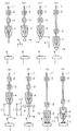
【発明の実施の形態】
本発明の一実施の形態を図1及び図2により説明する。図1(a)に示すように、ワイヤ1は、第2ワイヤクランパ2及び第1ワイヤクランパ3を通してキャピラリ4に挿通され、キャピラリ4の下端より延在している。この状態においては、第2ワイヤクランパ2が開き、第1ワイヤクランパ3が閉じた状態にある。ここで、第2ワイヤクランパ2は上下動しなく、第1ワイヤクランパ3はキャピラリ4と共に上下動するようになっている。この状態で図1(b)に示すように、ワイヤ1の先端に電気トーチ5による放電によってボール1aを作る。その後、電気トーチ5は矢印方向へ移動する。
【0015】
次に図1(c)に示すように、第1ワイヤクランパ3が開く。これにより、ワイヤ1に掛けられているバックテンションの作用によってボール1aがキャピラリ4の下端に当接する。続いて図1(d)に示すように、キャピラリ4及び第1ワイヤクランパ3が長さL1だけ下降する。次に図1(e)に示すように、第2ワイヤクランパ2が閉じ、キャピラリ4及び第1ワイヤクランパ3が元の位置に上昇、即ち長さL1だけ上昇する。これにより、キャピラリ4の下端からワイヤ1が長さL1だけ延在する。
【0016】
次に図1(f)に示すように、第1ワイヤクランパ3が閉じた後に第2ワイヤクランパ2が開き、キャピラリ4の下端より長さL2だけ下方に配設されている図示しないワイヤボンディング装置に設けたカッター6が往復動作してワイヤ1を切断する箇所に傷1bを付ける。この時、カッター6がワイヤ1に対向するように当接してほぼ等しく喰い込むので、傷1bは対向した位置にほぼ等しい大きさで付けられる。
【0017】
カッター6が退避した後、図1(g)に示すように、第1ワイヤクランパ3が開き、キャピラリ4及び第1ワイヤクランパ3が下降し、ボール1aをIC、LSI等の電子回路素子7の電極パッド8に圧接させる。次にキャピラリ4に超音波振動を印加し、ボール1aを電極パッド8にボンディングし、ボール1aは圧着ボール1cとなる。
【0018】
次に図1(h)に示すように、キャピラリ4と第1ワイヤクランパ3が共に上昇し、この上昇途中で第1ワイヤクランパ3が閉じる。これにより、傷1b部分よりワイヤ1が切断され、ピン状ワイヤ10が形成される。この場合、第1ワイヤクランパ3が閉じるタイミングは、キャピラリ4がピン状ワイヤ10内で、キャピラリ4は次の図2に示す工程で形成する湾曲状ワイヤ11(図2(g)参照)の形成工程のスタート位置まで上昇した時である。前記傷1b部分はワイヤ1の対抗する位置に等しい大きさで付けられているので、切断面はばらつかずに一様となり、またピン状ワイヤ10の長さは安定し、一定量の長さL4が得られる。
【0019】
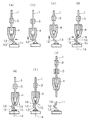
次に湾曲状ワイヤ11の形成方法を図2により説明する。なお、図2(a)乃至(f)は第2ワイヤクランパ2を省略して図示した。図1(h)の状態より図2(a)に示すように、キャピラリ4及び第1ワイヤクランパ3は水平に移動する。これにより、キャピラリ4の下端に当接する第1湾曲部12に癖が付き、圧着ボール1cから第1湾曲部12までに第1傾斜部13が形成される。続いて図2(b)に示すように、キャピラリ4及び第1ワイヤクランパ3は約100μm程度下降する。これにより、第1傾斜部13がキャピラリ4の下面により押し下げられる。次に図2(c)に示すように、キャピラリ4及び第1ワイヤクランパ3は上昇する。
【0020】
ここで、図2(b)の工程を行わないで、図2(a)の工程より図2(c)の工程を行うと、第1傾斜部13の弾性により第1傾斜部13の傾斜角度(形状)が変化する。本実施の形態のように、図2(a)の工程と図2(c)の工程間に図2(b)の工程を行うことにより、第1傾斜部13の弾性変形分を吸収するので、図2(c)のようにキャピラリ4が上昇した時に第1傾斜部13の傾斜角度(形状)が安定する。
【0021】
次に図2(d)に示すように、キャピラリ4及び第1ワイヤクランパ3は図2(a)に示す移動方向と逆方向に水平に圧着ボール1cの中心線14上より僅かに(約100μm程度)多く移動する。これにより、キャピラリ4の下端に当接する第2湾曲部15に癖が付き、第1湾曲部12から第2湾曲部15までに前記第1傾斜部13と逆方向の第2傾斜部16が形成される。続いて図2(e)に示すように、キャピラリ4及び第1ワイヤクランパ3は約100μm程度下降する。これにより、第2傾斜部16がキャピラリ4の下面により押し下げられる。次に図2(f)に示すように、圧着ボール1cの中心線14上に斜めに上昇する。前記図2(e)の工程により、前記した図2(b)の工程と同様に、第2傾斜部16の傾斜角度(形状)が安定する。
【0022】
次に図2(g)に示すように、第2ワイヤクランパ2が閉じ、第1ワイヤクランパ3が開き、キャピラリ4及び第1ワイヤクランパ3は上昇し、キャピラリ4の下端よりワイヤ1が延在する。次に第2ワイヤクランパ2が開き、第1ワイヤクランパ3が閉じ、次の電極パッド8の上方に移動し、図1(a)の状態となる。これにより、湾曲状ワイヤ11が形成される。以後、図1(a)乃至(h)、図2(a)乃至(g)の工程を行い、順次湾曲状ワイヤ11を形成する。
【0023】
このように、本実施の形態においては、まず図1(h)に示すように、ワイヤ1より切断されたピン状ワイヤ10を形成し、このピン状ワイヤ10に図2(a)乃至(g)に示す工程で湾曲状ワイヤ11を形成するので、この湾曲状ワイヤ11形成時には、ワイヤ1に予め掛けられているバックテンションが全く作用しなく、形成された湾曲状ワイヤ11が変形することがない。また湾曲状ワイヤ11の第1傾斜部13及び第2傾斜部16を形成する場合、図2(b)及び(e)に示すようにキャピラリ4を僅かに下降させて押し下げる工程を設けることにより、更に安定した湾曲状ワイヤ11が得られる。
【0024】
またピン状ワイヤ10を形成する場合、図1(f)に示すように、ワイヤ1にカッター6で傷1bを付ける工程は、ボール1aを電極パッド8にボンディングするためにキャピラリ4が下降する前に行われる。従って、電極パッド8とキャピラリ4間はカッター6を配設するのに十分な間隔があり、何ら支障はない。また既に密集して図2(g)に示す湾曲状ワイヤ11が形成されている場合も、カッター6は湾曲状ワイヤ11より離れた上方で作動するので、カッターが湾曲状ワイヤ11に接触することもない。これらのことにより、傷1bを付けるワイヤ1の部分に制限はなく、ピン状ワイヤ10の長さL3を任意に設定できる。
【0025】
また第2ワイヤクランパ2を用いることにより、図1(e)に示すようにキャピラリ4の下端より一定量の長さL1だけワイヤ1を延在させることができるので、図1(f)に示すように予め決められたワイヤ1の長さL3の位置に傷1bを付けることができる。これにより、ボール1aから傷1bまでの長さL3は安定した一定量となる。従って、図1(h)に示すように形成されたピン状ワイヤ10の長さが一定となり、前記長さL3とほぼ等しい安定した一定量の長さL4が得られる。
【0026】
図3は本発明の他の実施の形態を示す。本実施の形態は、ワイヤボンディング装置による一連の工程で湾曲状ワイヤ11を形成した。本実施の形態は、ワイヤボンディング装置でピン状ワイヤ10を予め形成し、その後別工程でワイヤボンディング装置の空のキャピラリ4(ワイヤ1が挿通されていないキャピラリ4)で湾曲状ワイヤ11を形成する。
【0027】
まず、図3(a)に示すピン状ワイヤ10の形成方法について説明する。このピン状ワイヤ10の形成は、図1(a)乃至(g)及び図3(a)の工程によって形成する。即ち、前記実施の形態の図1(h)の工程が図3(a)の工程に変わるのみである。そこで、図1(a)乃至(g)までの工程の説明は省略し、図1(g)の工程が終わった状態から説明する。
【0028】
図1(g)に示すように、ボール1aを電極パッド8にボンディングし、ボール1aは圧着ボール1cとなる。次にキャピラリ4が図1(g)に示す傷1bより上方に第1ワイヤクランパ3が共に上昇し、この上昇途中で第1ワイヤクランパ3が閉じる。これにより、図3(a)に示すように、傷1b部分よりワイヤ1が切断され、ピン状ワイヤ10が形成され、またキャピラリ4の下面よりワイヤ1が延在する。この図1(a)乃至(g)及び図3(a)の工程を行い、順次ピン状ワイヤ10を形成する。
【0029】
次に湾曲状ワイヤ11の形成方法を図3(b)乃至(j)により説明する。本実施の形態の図3(d)乃至(j)は、それぞれ前記実施の形態の図2(a)乃至(g)に対応する。即ち、図2(a)乃至(g)においては、キャピラリ4内にワイヤ1の下方部が位置していたが、図3(d)乃至(j)においては、ワイヤ1がない点が異なっている。
【0030】
まず、図3(b)に示すように、ピン状ワイヤ10の上方に空のキャピラリ4が位置し、続いてキャピラリ4が下降し、図3(c)に示すようにキャピラリ4にピン状ワイヤ10が挿通される。
【0031】
次に図3(d)に示すように、キャピラリ4は矢印で示す水平方向に移動する。これにより、キャピラリ4の下端に当接する第1湾曲部12に癖が付き、圧着ボール1cから第1湾曲部12までに第1傾斜部13が形成される。続いて図3(e)に示すように、キャピラリ4は約100μm程度下降する。これにより、第1傾斜部13がキャピラリ4の下面により押し下げられる。次に図3(f)に示すように、キャピラリ4は上昇する。
【0032】
次に図3(g)に示すように、キャピラリ4は前記と逆方向に矢印で示す水平方向に圧着ボール1cの中心線14上より僅かに(約100μm程度)多く移動する。これにより、キャピラリ4の下端に当接する第2湾曲部15に癖が付き、第1湾曲部12から第2湾曲部15までに前記第1傾斜部13と逆方向の第2傾斜部16が形成される。続いて図3(h)に示すように、キャピラリ4は約100μm程度下降する。これにより、第2傾斜部16がキャピラリ4の下面により押し下げられる。次に図3(i)に示すように、圧着ボール1cの中心線14上に矢印で示す斜め方向に上昇する。
【0033】
次に図3(j)に示すように、キャピラリ4は上昇し湾曲状ワイヤ11が形成される。以後、図3(b)乃至(j)の工程を行い、ピン状ワイヤ10に順次湾曲状ワイヤ11を形成する。
【0034】
本実施の形態においても前記実施の形態と同様に、まず図3(a)に示すように、ワイヤ1より切断されたピン状ワイヤ10を形成し、このピン状ワイヤ10に図3(b)乃至(j)に示す工程で湾曲状ワイヤ11を形成するので、この湾曲状ワイヤ11形成時には、ワイヤ1に予め掛けられているバックテンションが全く作用しなく、形成された湾曲状ワイヤ11が変形することがない。また湾曲状ワイヤ11の第1傾斜部13及び第2傾斜部16を形成する場合、図3(e)及び(h)に示すようにキャピラリ4を僅かに下降させて押し下げる工程を設けることにより、更に安定した湾曲状ワイヤ11が得られる。
【0035】
なお、図1及び図2に示す実施の形態においては、一連の工程で湾曲状ワイヤ11を形成したので、図1(f)に示すように予め切断位置に傷1bを付ける必要があった。しかし、図3に示す実施の形態においては、ピン状ワイヤ10を形成し、その後に空のキャピラリ4で湾曲状ワイヤ11を形成するので、ピン状ワイヤ10の形成方法は、前記した図1(a)乃至(g)、図3(a)の工程に限定されない。例えば図4に示す方法によってピン状ワイヤ10を形成してもよい。
【0036】
図4(a)に示すように、ワイヤ1は、第2ワイヤクランパ2及び第1ワイヤクランパ3を通してキャピラリ4に挿通され、キャピラリ4の下端より延在している。この状態においては、第2ワイヤクランパ2が開き、第1ワイヤクランパ3が閉じた状態にある。この状態で図4(b)に示すように、ワイヤ1の先端に電気トーチ5による放電によってボール1aを作る。その後、電気トーチ5は矢印方向へ移動する。
【0037】
次に図4(c)に示すように、第1ワイヤクランパ3が開く。これにより、ワイヤ1に掛けられているバックテンションの作用によってボール1aがキャピラリ4の下端に当接する。続いて図4(d)に示すように、キャピラリ4及び第1ワイヤクランパ3が下降し、ボール1aをIC、LSI等の電子回路素子7の電極パッド8に圧接させる。次にキャピラリ4に超音波振動を印加し、ボール1aを電極パッド8にボンディングし、ボール1aは圧着ボール1cとなる。
【0038】
次に図4(e)に示すように、キャピラリ4及び第1ワイヤクランパ3は、ピン状ワイヤ10の長さ及びテール長さ分だけ上昇する。続いて図4(f)に示すように、第1ワイヤクランパ3が閉じた後、カッター6が往復移動してワイヤ1を切断する。カッター6が退避した後、図4(g)に示すように、キャピラリ4及び第1ワイヤクランパ3が上昇し、ピン状ワイヤ10が形成される。このような方法でピン状ワイヤ10を形成してもよい。
【0039】
【発明の効果】
本発明の第1の手段は、ワイヤボンディング装置によりピン状ワイヤを形成し、このピン状ワイヤにキャピラリを挿通した状態で、キャピラリの軌跡が湾曲状になるように移動させて湾曲状ワイヤを形成するので、ワイヤに掛けられたバックテンションの影響を受けなく、安定した高品質の形状が得られる。
【0040】
本発明の第2又は第3の手段は、ワイヤボンディング装置によりピン状ワイヤを形成し、この状態において、前記ピン状ワイヤにキャピラリが挿通され、かつピン状ワイヤより分離されたワイヤもキャピラリ内にあり、キャピラリの軌跡が湾曲状になるように移動させて湾曲状ワイヤを形成するか、またはワイヤボンディング装置によりピン状ワイヤを形成し、このピン状ワイヤに空のキャピラリが挿通し、キャピラリの軌跡が湾曲状になるように移動させて湾曲状ワイヤを形成するので、前記第1の手段と同じ効果が得られる。
【0041】
本発明の第4の手段は、上記第1、第2又は第3の手段において、前記キャピラリを移動させて前記ピン状ワイヤに癖を付けて傾斜部を形成した後に、キャピラリを僅かに下降させて該キャピラリで前記傾斜部を押し下げる工程を有するので、前記効果の他に、有する余分な弾性力を吸収して一定量の弾性力とし、更に安定した高品質の形状が得られる。
【0042】
本発明の第5の手段は、上記第1、第2又は第3の手段において、前記ピン状ワイヤの形成は、キャピラリに挿通されたワイヤの先端にボールを形成した後、キャピラリの下端よりワイヤを延在させ、ワイヤボンディング装置に設けた傷付け手段によって前記ボールと前記キャピラリ間のワイヤ部分に傷を付け、前記ボールを前記キャピラリを用いて電子回路素子等の電極パッドにボンディングし、次にキャピラリを上昇させた後に、ワイヤを上方に引っ張って前記傷部分よりワイヤを切断して形成するので、前記第1の手段の効果の他に、電子回路素子等にボンディングされたボールより上方のワイヤ長さを任意に設定でき、またコスト高になることもないと共に、ピン状ワイヤの長さが一定となり、安定した一定量の長さとなる。
【図面の簡単な説明】
【図1】本発明の湾曲状ワイヤの形成方法の一実施の形態におけるピン状ワイヤ形成を示す工程図である。
【図2】図1の続きの工程で、本発明の湾曲状ワイヤの形成の一実施の形態を示す工程図である。
【図3】本発明の湾曲状ワイヤの形成方法の他の実施の形態を示す工程図である。
【図4】ピン状ワイヤ形成の他の実施の形態を示す工程図である。
【符号の説明】
1 ワイヤ
1a ボール
1b 傷
1c 圧着ボール
2 第2ワイヤクランパ
3 第1ワイヤクランパ
4 キャピラリ
5 電気トーチ
6 カッター
7 電子回路素子
8 電極パッド
10 ピン状ワイヤ
11 湾曲状ワイヤ
12 第1湾曲部
13 第1傾斜部
15 第2湾曲部
16 第2傾斜部[0001]
BACKGROUND OF THE INVENTION
The present invention relates to a method for forming a curved wire.
[0002]
[Prior art]
Conventionally, as a method for forming a curved wire having a curved portion with a wire bonding apparatus, for example, a method disclosed in Japanese Patent Application Laid-Open No. 11-514493 is cited. In this method, a ball is formed at the tip of a wire that is inserted through a capillary and extends from the lower surface of the capillary, and the capillary is lowered to bond the ball to an electrode pad. Thereafter, the capillary trajectory is moved in a curved shape to form a curved wire shape. Next, the capillary is raised above the wire cutting position, and the wire is cut by mechanical means such as electronic flame injection or a knife to form a curved wire.
[0003]
[Problems to be solved by the invention]
In the wire bonding apparatus, a back tension is applied to a wire inserted through a capillary, and a constant tension is applied to the wire. A wire clamper is provided above the capillary to hold the wire.
[0004]
The prior art described above has the following problems because the wire is cut after the capillary is moved to form the shape of the curved wire. When the capillary is moved to form a curved wire shape, the wire clamper is in an open state because the wire needs to be fed out from the capillary. For this reason, due to the back tension applied to the wire, the shape of the curved wire before cutting is pulled upward and deformed, and a stable shape cannot be obtained. In addition, since the shape of the curved wire is formed by moving the capillary along the shape of the curved wire that is simply formed, the shape of the curved portion and the inclined portion of the curved wire is deformed by the elastic force of the wire. Therefore, a stable shape cannot be obtained.
[0005]
A first object of the present invention is to provide a method for forming a curved wire that is not affected by the back tension applied to the wire and can obtain a stable and high-quality shape.
[0006]
A second object of the present invention is to provide a method for forming a curved wire that absorbs an extra elastic force of the wire to obtain a certain amount of elastic force, and can obtain a stable and high-quality shape.
[0007]
The third problem of the present invention is that the wire length above the ball bonded to the electronic circuit element or the like can be arbitrarily set, the cost is not increased, and the length of the pin-shaped wire is constant, It is an object of the present invention to provide a method of forming a curved wire having a stable and constant length.
[0008]
[Means for Solving the Problems]
The first means of the present invention for solving the first problem is that a pin-shaped wire is formed by a wire bonding apparatus, and the capillary trajectory is curved in a state where the capillary is inserted into the pin-shaped wire. It is made to move so that a curved wire may be formed.
[0009]
The second means of the present invention for solving the first problem is that a pin-shaped wire is formed by a wire bonding apparatus, and in this state, a capillary is inserted into the pin-shaped wire and separated from the pin-shaped wire. The curved wire is also in the capillary and is moved so that the locus of the capillary is curved to form a curved wire.
[0010]
According to a third means of the present invention for solving the first problem, a pin-shaped wire is formed by a wire bonding apparatus, an empty capillary is inserted into the pin-shaped wire, and the capillary trajectory becomes curved. It is made to move so that a curved wire may be formed.
[0011]
According to a fourth means of the present invention for solving the first and second problems, in the first, second, or third means, the capillary is moved to hook the pin-shaped wire. After the inclined portion is formed, the method includes a step of slightly lowering the capillary and pushing down the inclined portion with the capillary.
[0012]
According to a fifth means of the present invention for solving the first and third problems, in the first, second or third means, the pin-shaped wire is formed by using a wire inserted through a capillary. After forming the ball at the tip, the wire is extended from the lower end of the capillary, and the wire portion between the ball and the capillary is scratched by the scratching means provided in the wire bonding apparatus. After bonding to an electrode pad such as a circuit element and then raising the capillary, the wire is pulled upward to cut the wire from the scratched portion.
[0013]
According to a sixth means of the present invention for solving the first and third problems, in the first, second, or third means, the formation of the pin-shaped wire is a first that moves up and down together with the capillary. Using a wire bonding apparatus having a wire clamper and a second wire clamper that does not move up and down, a wire is inserted through the capillary through the second wire clamper and the first wire clamper, the second wire clamper is opened, and the first wire clamper is closed. In this state, after forming a ball at the tip of the wire inserted into the capillary, the first wire clamper is opened, and the ball abuts on the lower end of the capillary by the action of the back tension applied to the wire. After the capillary and the first wire clamper are lowered, and then the second wire clamper is closed, the capillary and the first wire clamper are closed. The wire is extended from the lower end of the capillary by raising the clamper, then the first wire clamper is closed and the second wire clamper is opened, and the wire between the ball and the capillary is provided by the scratching means provided in the wire bonding apparatus. Next, the first wire clamper is opened to lower the capillary and the first wire clamper, and the ball is bonded to an electrode pad of an electronic circuit element or the like using the capillary. One wire clamper is raised, and the first wire clamper is closed in the middle of the raising, and the wire is pulled upward to cut the wire from the scratched portion.
[0014]
DETAILED DESCRIPTION OF THE INVENTION
An embodiment of the present invention will be described with reference to FIGS. As shown in FIG. 1A, the
[0015]
Next, as shown in FIG. 1C, the
[0016]
Next, as shown in FIG. 1 (f), the
[0017]
After the
[0018]
Next, as shown in FIG. 1 (h), both the
[0019]
Next, a method of forming the
[0020]
Here, if the step of FIG. 2C is performed from the step of FIG. 2A without performing the step of FIG. 2B, the inclination angle of the first
[0021]
Next, as shown in FIG. 2D, the
[0022]
Next, as shown in FIG. 2G, the
[0023]
Thus, in the present embodiment, first, as shown in FIG. 1 (h), the pin-shaped
[0024]
When forming the pin-shaped
[0025]
Further, by using the
[0026]
FIG. 3 shows another embodiment of the present invention. In the present embodiment, the
[0027]
First, a method for forming the pin-shaped
[0028]
As shown in FIG. 1G, the ball 1a is bonded to the
[0029]
Next, a method for forming the
[0030]
First, as shown in FIG. 3 (b), and empty the capillary 4 is positioned above the pin-
[0031]
Next, as shown in FIG. 3D, the
[0032]
Next, as shown in FIG. 3G, the
[0033]
Next, as shown in FIG. 3 (j), the
[0034]
Also in this embodiment, as in the above embodiment, first, as shown in FIG. 3A, a pin-
[0035]
In the embodiment shown in FIGS. 1 and 2, since the
[0036]
As shown in FIG. 4A, the
[0037]
Next, as shown in FIG. 4C, the
[0038]
Next, as shown in FIG. 4E, the
[0039]
【The invention's effect】
According to the first means of the present invention, a pin-shaped wire is formed by a wire bonding apparatus, and in the state where the capillary is inserted through the pin-shaped wire, the capillary trajectory is moved to form a curved wire. Therefore, a stable high quality shape can be obtained without being affected by the back tension applied to the wire.
[0040]
In the second or third means of the present invention, a pin-shaped wire is formed by a wire bonding apparatus, and in this state, a capillary is inserted into the pin-shaped wire, and the wire separated from the pin-shaped wire is also in the capillary. Yes, the capillary trajectory is moved to form a curved wire to form a curved wire, or a pin-shaped wire is formed by a wire bonding apparatus, and an empty capillary is inserted through this pin-shaped wire, and the capillary trajectory Since the curved wire is formed by moving the wire so as to be curved, the same effect as the first means can be obtained.
[0041]
According to a fourth means of the present invention, in the first, second or third means, the capillary is moved and the pin-shaped wire is hooked to form an inclined portion, and then the capillary is slightly lowered. In addition to the above-described effect, the capillary has a step of pushing down the inclined portion. In addition to the above effect, the extra elastic force is absorbed to obtain a certain amount of elastic force, and a more stable high quality shape can be obtained.
[0042]
According to a fifth means of the present invention, in the first, second or third means, the pin-shaped wire is formed by forming a ball at the tip of the wire inserted through the capillary and then starting from the lower end of the capillary. The wire portion between the ball and the capillary is scratched by a scratching means provided in the wire bonding apparatus, the ball is bonded to an electrode pad of an electronic circuit element or the like using the capillary, and then the capillary In addition to the effect of the first means, the wire length above the ball bonded to the electronic circuit element or the like is formed by pulling the wire upward and cutting the wire from the scratched portion. The length can be set arbitrarily, and the cost is not increased, and the length of the pin-shaped wire is constant, and the length is stable and constant.
[Brief description of the drawings]
FIG. 1 is a process diagram showing pin-shaped wire formation in an embodiment of a method for forming a curved wire of the present invention.
FIG. 2 is a process diagram showing an embodiment of the formation of the curved wire of the present invention in the process subsequent to FIG. 1;
FIG. 3 is a process diagram showing another embodiment of the method for forming a curved wire of the present invention.
FIG. 4 is a process diagram showing another embodiment of forming a pin-shaped wire.
[Explanation of symbols]
DESCRIPTION OF
Claims (6)
Priority Applications (4)
| Application Number | Priority Date | Filing Date | Title |
|---|---|---|---|
| JP2000084863A JP4088015B2 (en) | 2000-03-24 | 2000-03-24 | Method for forming curved wire |
| TW089126700A TW522497B (en) | 2000-03-24 | 2000-12-14 | Method of forming bent wire |
| KR10-2001-0012329A KR100424166B1 (en) | 2000-03-24 | 2001-03-09 | Method for forming curve-form wire |
| US09/814,189 US6564453B2 (en) | 2000-03-24 | 2001-03-21 | Bent wire forming method |
Applications Claiming Priority (1)
| Application Number | Priority Date | Filing Date | Title |
|---|---|---|---|
| JP2000084863A JP4088015B2 (en) | 2000-03-24 | 2000-03-24 | Method for forming curved wire |
Publications (3)
| Publication Number | Publication Date |
|---|---|
| JP2001274186A JP2001274186A (en) | 2001-10-05 |
| JP2001274186A5 JP2001274186A5 (en) | 2006-07-27 |
| JP4088015B2 true JP4088015B2 (en) | 2008-05-21 |
Family
ID=18601281
Family Applications (1)
| Application Number | Title | Priority Date | Filing Date |
|---|---|---|---|
| JP2000084863A Expired - Fee Related JP4088015B2 (en) | 2000-03-24 | 2000-03-24 | Method for forming curved wire |
Country Status (4)
| Country | Link |
|---|---|
| US (1) | US6564453B2 (en) |
| JP (1) | JP4088015B2 (en) |
| KR (1) | KR100424166B1 (en) |
| TW (1) | TW522497B (en) |
Families Citing this family (11)
| Publication number | Priority date | Publication date | Assignee | Title |
|---|---|---|---|---|
| US7229906B2 (en) * | 2002-09-19 | 2007-06-12 | Kulicke And Soffa Industries, Inc. | Method and apparatus for forming bumps for semiconductor interconnections using a wire bonding machine |
| JP4509043B2 (en) * | 2006-02-14 | 2010-07-21 | 株式会社新川 | Stud bump formation method |
| CN101505905A (en) * | 2006-10-18 | 2009-08-12 | 库利克和索夫工业公司 | Improved conductive bumps, wire loops including the improved conductive bumps, and methods of forming the same |
| JP4467631B1 (en) * | 2009-01-07 | 2010-05-26 | 株式会社新川 | Wire bonding method |
| US8177495B2 (en) * | 2009-03-24 | 2012-05-15 | General Electric Company | Method and apparatus for turbine interstage seal ring |
| CN102437111B (en) * | 2011-12-01 | 2014-03-26 | 中南大学 | Method and device for quickly forming arc for leading wire by using wire clamp to manufacture salient points |
| US9082753B2 (en) * | 2013-11-12 | 2015-07-14 | Invensas Corporation | Severing bond wire by kinking and twisting |
| US9087815B2 (en) * | 2013-11-12 | 2015-07-21 | Invensas Corporation | Off substrate kinking of bond wire |
| TWI543284B (en) * | 2014-02-10 | 2016-07-21 | 新川股份有限公司 | Method for producing semiconductor apparatus and wire bonding apparatus |
| WO2022259329A1 (en) * | 2021-06-07 | 2022-12-15 | 株式会社新川 | Semiconductor device manufacturing method and wire bonding device |
| TWI824354B (en) * | 2021-12-15 | 2023-12-01 | 日商新川股份有限公司 | Wire bonding device, wire cutting method and program |
Family Cites Families (6)
| Publication number | Priority date | Publication date | Assignee | Title |
|---|---|---|---|---|
| US5917707A (en) * | 1993-11-16 | 1999-06-29 | Formfactor, Inc. | Flexible contact structure with an electrically conductive shell |
| US5476211A (en) * | 1993-11-16 | 1995-12-19 | Form Factor, Inc. | Method of manufacturing electrical contacts, using a sacrificial member |
| US5813115A (en) * | 1994-08-03 | 1998-09-29 | Matsushita Electric Industrial Co., Ltd. | Method of mounting a semiconductor chip on a wiring substrate |
| US5734546A (en) * | 1994-09-21 | 1998-03-31 | Rohm Co. Ltd. | Capacitor element for solid electrolytic capacitor and process for making the same |
| AU4160096A (en) | 1994-11-15 | 1996-06-06 | Formfactor, Inc. | Probe card assembly and kit, and methods of using same |
| JP3189115B2 (en) * | 1996-12-27 | 2001-07-16 | 株式会社新川 | Semiconductor device and wire bonding method |
-
2000
- 2000-03-24 JP JP2000084863A patent/JP4088015B2/en not_active Expired - Fee Related
- 2000-12-14 TW TW089126700A patent/TW522497B/en not_active IP Right Cessation
-
2001
- 2001-03-09 KR KR10-2001-0012329A patent/KR100424166B1/en not_active IP Right Cessation
- 2001-03-21 US US09/814,189 patent/US6564453B2/en not_active Expired - Fee Related
Also Published As
| Publication number | Publication date |
|---|---|
| JP2001274186A (en) | 2001-10-05 |
| KR20010092682A (en) | 2001-10-26 |
| KR100424166B1 (en) | 2004-03-24 |
| US20010023534A1 (en) | 2001-09-27 |
| US6564453B2 (en) | 2003-05-20 |
| TW522497B (en) | 2003-03-01 |
Similar Documents
| Publication | Publication Date | Title |
|---|---|---|
| JP3566156B2 (en) | Method for forming pin-shaped wires | |
| JP3513444B2 (en) | Method for forming pin-shaped wires | |
| JP4088015B2 (en) | Method for forming curved wire | |
| JP2006222128A (en) | Wire bonding method | |
| KR19980070182A (en) | Bump Formation Method | |
| JPH11251350A (en) | Method and apparatus for forming bump | |
| JP4509043B2 (en) | Stud bump formation method | |
| JP2000114304A (en) | Wire bonding method | |
| JPH09162228A (en) | Method of wire bonding for coated wire | |
| JPH09148360A (en) | Wire bonding apparatus and method for covered wire | |
| JP2004247674A (en) | Method for wire bonding | |
| JP3377747B2 (en) | Wire bonding method | |
| JP4021378B2 (en) | Wire bonding method | |
| JP3218382B2 (en) | Wire bonding method of coated wire | |
| JP3128717B2 (en) | Bump forming method | |
| JP3074518B2 (en) | Wire bonding method of coated wire | |
| JP2977990B2 (en) | Wire bonding method | |
| JP2000114303A (en) | Wire bonding method | |
| JP3346192B2 (en) | Method of forming bump | |
| JP4313958B2 (en) | Wire bonding method | |
| JP2579833B2 (en) | Wire bonding method | |
| JP2894344B1 (en) | Wire bonding method | |
| JP2925392B2 (en) | Ball type wire bonding method | |
| JP2976645B2 (en) | Bump forming method | |
| JPH0572105B2 (en) |
Legal Events
| Date | Code | Title | Description |
|---|---|---|---|
| A521 | Request for written amendment filed |
Free format text: JAPANESE INTERMEDIATE CODE: A523 Effective date: 20060613 |
|
| A621 | Written request for application examination |
Free format text: JAPANESE INTERMEDIATE CODE: A621 Effective date: 20060613 |
|
| A977 | Report on retrieval |
Free format text: JAPANESE INTERMEDIATE CODE: A971007 Effective date: 20080125 |
|
| TRDD | Decision of grant or rejection written | ||
| A01 | Written decision to grant a patent or to grant a registration (utility model) |
Free format text: JAPANESE INTERMEDIATE CODE: A01 Effective date: 20080212 |
|
| A61 | First payment of annual fees (during grant procedure) |
Free format text: JAPANESE INTERMEDIATE CODE: A61 Effective date: 20080222 |
|
| FPAY | Renewal fee payment (event date is renewal date of database) |
Free format text: PAYMENT UNTIL: 20110228 Year of fee payment: 3 |
|
| R150 | Certificate of patent or registration of utility model |
Free format text: JAPANESE INTERMEDIATE CODE: R150 |
|
| LAPS | Cancellation because of no payment of annual fees |