JP4087236B2 - Switch device, integrated circuit, digital transmission system, and auto switch - Google Patents
Switch device, integrated circuit, digital transmission system, and auto switch Download PDFInfo
- Publication number
- JP4087236B2 JP4087236B2 JP2002355006A JP2002355006A JP4087236B2 JP 4087236 B2 JP4087236 B2 JP 4087236B2 JP 2002355006 A JP2002355006 A JP 2002355006A JP 2002355006 A JP2002355006 A JP 2002355006A JP 4087236 B2 JP4087236 B2 JP 4087236B2
- Authority
- JP
- Japan
- Prior art keywords
- interconnection
- matrix
- binary
- switch device
- switch
- Prior art date
- Legal status (The legal status is an assumption and is not a legal conclusion. Google has not performed a legal analysis and makes no representation as to the accuracy of the status listed.)
- Expired - Fee Related
Links
Images


Classifications
-
- H—ELECTRICITY
- H04—ELECTRIC COMMUNICATION TECHNIQUE
- H04L—TRANSMISSION OF DIGITAL INFORMATION, e.g. TELEGRAPHIC COMMUNICATION
- H04L49/00—Packet switching elements
- H04L49/35—Switches specially adapted for specific applications
- H04L49/356—Switches specially adapted for specific applications for storage area networks
- H04L49/357—Fibre channel switches
-
- H—ELECTRICITY
- H04—ELECTRIC COMMUNICATION TECHNIQUE
- H04L—TRANSMISSION OF DIGITAL INFORMATION, e.g. TELEGRAPHIC COMMUNICATION
- H04L49/00—Packet switching elements
- H04L49/10—Packet switching elements characterised by the switching fabric construction
- H04L49/101—Packet switching elements characterised by the switching fabric construction using crossbar or matrix
Landscapes
- Engineering & Computer Science (AREA)
- Computer Networks & Wireless Communication (AREA)
- Signal Processing (AREA)
- Use Of Switch Circuits For Exchanges And Methods Of Control Of Multiplex Exchanges (AREA)
- Data Exchanges In Wide-Area Networks (AREA)
Description
【0001】
【発明の属する技術分野】
本発明は高速伝送用の集積回路に関する。詳細には、本発明は、制御部材で制御される相互接続点マトリクスにより相互に接続される複数の入力端及び出力端を備え、所定のスイッチング方式に従って、前記入力端から前記出力端に伝送路を介して電気信号を伝送するものであり、また、各伝送路が前記電気信号を伝送するための信号経路と、電圧基準経路と呼ばれる所定の電圧が供給されている基準経路とを備える。
【0002】
本発明は、また、そのような装置を含む集積回路に関する。本発明はまた、複数の送信機及び受信機を相互接続するスイッチ装置を組み込んでいるオートスイッチを備えた、ディジタル伝送システムに関する。最後に、本発明はディジタル伝送システムのオートスイッチに関する。
【0003】
本発明は多くの用途、特に光接続を使用する伝送システムでの用途に利用できる。本発明は、特に、高速パケット交換への用途において有利である。
【0004】
【従来の技術】
光伝送に使用される集積回路は、電気信号を高速で、例えば、約10ギガビット毎秒のオーダーで伝送することができる。このような伝送速度では、回路の入力端と出力端との間の接続には、回路性能に関して無視できない有害な影響を与える線路損が発生する。回路サイズの減少及びこれに伴う接続線の数と長さを減少させることは、線路損を減少させるため回路性能の改良に寄与する。これらの効果は高速用途ではさらに顕著である。なぜなら、高速伝送では、伝送路には高周波電流が流れ、この高周波電流により表皮効果として公知の特殊な効果が発生して、使用される材料の抵抗を増加させるからである。
【0005】
最初の文節で述べたタイプの従来のスイッチ装置は、入力端及び出力端の数におけるスイッチング・マトリクスのサイズとその容積の比を最適化しようとするものである。この装置は、カスケード接続構成で配置された複数のスイッチ素子を備え、各スイッチ素子が2つの入力端と2つの出力端とを有する多段マトリクス回路を形成している。スイッチ素子は、いくつかの部位又はスイッチング段階においてカスケード接続構成で相互に接続されており、それによりスイッチ素子のすべての入力端を、マトリクスの相互接続方式に応じて、1つ又はいくつかのスイッチング段階を介して別のスイッチ素子のすべての出力端に切り換えできるようにしている(特許文献1参照。)。
【0006】
【特許文献1】
欧州特許出願公開第1014625号明細書
【0007】
【発明が解決しようとする課題】
上述した多段スイッチング・マトリクスは、実現化と制御が比較的複雑である。なぜなら、マトリクスのすべての入力端とすべての出力端との間の直接固有接続路が存在しないからである。このようなマトリクスの実現、制御、及びプログラムは、例えば高速パケット交換用途で使用する場合には、使用がかなり複雑になる。さらに、いくつかのステージのカスケード接続構成におけるこのようなマトリクスの構造は、回路の性能に対し、特にジッターの点で有害である。
【0008】
本発明の目的は、上述した従来の装置に比べて優れた性能を有し、かつ実現化及び制御が容易である、高速用途に使用する小容積のスイッチ装置を提供することである。本発明では、マトリクスの個々の構成要素の管理方法を変更することにより、既に存在している特定の構成要素を、マトリクス上でそれらの構成要素を繰返し利用することにより、個々の構成要素に適合させて再使用し、マトリクスで占有される全体スペースの大幅な低減を図るようにしている。
【0009】
【課題を解決するための手段】
この目的のため、最初の文節で述べたタイプの装置が提供される。この装置は、前記相互接続点をマトリクスで配置することにより、2つの別個の伝送路が1つの共通電圧基準経路を持つようにしていることを特徴とする。この構成により、1つの電圧基準経路により占有されるスペースを、少なくとも、マトリクス上に存在する出力端対の数倍にまで節減できる。
【0010】
特定の実施形態によれば、相互接続点は相互接続点の対で配置され、それにより2つの隣接する相互接続点の対が1つの共通電圧基準経路を持つようになっている。
【0011】
本発明の別の実施形態によれば、スイッチング方式に従って所定の制御信号を用いてマトリクスの動作を制御する制御部材を備え、その制御部材の制御によって、所定の時点では、1つの出力端だけが、アクティブ状態と呼ばれる第1のスイッチング状態に設定された特定の相互接続点により前記入力端の1つに接続できる。前記出力端に他の入力端を接続することが可能なその他の相互接続点のすべては、イナクティブ状態と呼ばれる第2のスイッチング状態に設定される。前記制御信号を復号して、前記相互接続点のスイッチング状態を導き出すための復号化手段を備えている。この実施形態によれば、復号化手段は相互接続点に組み合わされた複数のデコーダを備え、このデコーダにより、前記相互接続点の近傍で前記制御信号を局部的に復号する。制御信号の局部的な復号化により、制御部材と相互接続点との間に必要な制御接続点数の低減が可能になり、したがって、それら制御接続点により占有されるスペースが減少する。
【0012】
本発明の別の実施形態によれば、2つの出力端を有する単一の局部デコーダが使用され、このデコーダは、1つで同一の複合素子の相互接続点によって反転手段に組み合わされている。前記単一デコーダは、従来の構成により使用されるデコーダ全体に比べて、単純かつ小型である。前記対を構成する2つの相互接続点は、マトリクスの1つで同一出力端に接続できる。この結果、4個のデコーダ(各相互接続点につき1つ)の代わりに、4つの相互接続点の各複合素子につき、1個のデコーダ対を使用できる。したがって、不要になった2個のデコーダにより占有されていたスペースが節減できる。
【0013】
本発明のこれら及びその他の態様は、以下に述べる実施形態に関連する非限定的な事例により、明らかになり、解明されるであろう。
【0014】
【発明の実施の形態】
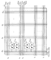
図1は、本発明に係るスイッチ装置の構成例を示す。この装置はn×m型の長方形マトリクス10で構成されており、ここでのnはI0からInで示される入力端の数を表わし、mはO0からOnで示される入力端の数を表わす。各入力端及び各出力端は別個の伝送路に接続されている。伝送路は、C00からCnmで(第1の添え字は入力端I0からInの添え字を示し、第2の添え字は対応する出力端O0からOmの添え字を示す)示される、マトリクスのスイッチ素子を構成する相互接続点の近傍で相互に接続されている。マトリクスの入力端の添え字iを持つ各伝送路は、SIiで示される信号経路で構成されており、前記信号経路の各々は電気信号をマトリクスの入力端Iiから伝送する。また、マトリクスの出力端の添え字jを持つ各伝送路は、SOjで示される信号経路で構成されており、前記信号経路の各々は電気信号をマトリクスの出力端Ojに伝送する。Vccで示される基準経路は、例えば2.5Vの電源電圧Vccの基準電圧が供給されている。電圧基準経路Vccは、例えば対応する信号経路Sj上に伝送される信号の帰還経路としての役割を果たすこともできる。またこの電圧基準経路Vccを別の目的、特に電磁遮蔽及び/又は電源供給経路として利用することができる。相互接続点又はスイッチ素子Ci、jは、入力端Iiに対応する信号経路SIiを出力端Ojに対応する信号経路SOjに移す機能を有する。単純化のために、図1では、相互接続点は単純な2方向スイッチで示している。しかし、相互接続点の機能を実行するために使用されるスイッチの型は、図1に示すスイッチCi、jに限定されない。図を単純化する同一目的のため、信号経路は単一ラインで示される。光伝送に対しては、各信号経路は2つの別個の並列の差動経路で構成される。すべての図に関して述べる本発明の原理は、差動伝送路にも適用される。
【0015】
本発明の原理によれば、相互接続点Ci、jはマトリクスで配置され、それにより2つの別個の伝送路が1つの共通電圧基準経路Vccを持つようになっている。図1では、1つで同一の出力伝送路SO0に接続可能な、一方ではスイッチ素子C0、0及びC1、0、他方ではC2、0及びC3、0は、対にグループ化され、それにより連続の添え字I1及びI2を持つマトリクスの2つの入力端に対応する伝送路が並んで配置されるようになる。1つで同一の電圧基準経路Vccは、対応する信号経路SI1とSI2との間に設けられる。この電圧基準経路は特に、2つの信号経路SI1及びSI2の共通帰還経路として役立つ。これにより、相互接続点の2つの対がこのように組み合わされている場合の、基準経路に必要な場所の節減と、ライン間の空き場所の節減とが可能になる。同一構成は、例えば、入力端I3とI4、次にI5とI6等に対応する伝送路に対して共通電圧基準経路を使用することにより、連続入力端に対応する伝送路の部位で再現できる。また同一原理はマトリクスの別の局面にも適用できる。この適用は、一方ではタイプCi、j及びCi、j+1、他方ではCi、j+2及びCi、j+3の相互接続点、タイプSIiの同一入力伝送路と、一方では連続添え字SOj及びSOj+1、他方では字SOj+2及びSOj+3と持つ出力端と接続可能な相互接続点を対にグループ化することによりなされる。
【0016】
図2に概略的に示す本発明による好ましい実施形態によれば、相互接続点は、4つの相互接続点の複合素子22にグループ化され、それにより2つの隣接素子22が1つの共通電圧基準経路を持つようになっている。図2は、4つの隣接複合素子を含むスイッチング・マトリクスの一部分だけを示す。本発明の有利な実施形態によれば、本発明の原理は、入力端と出力端の伝送路の部位で、2次元のマトリクスで適用される。同一素子は図1に示すものと同一参照符号である。基準経路Vccはこの場合には、マトリクスの2つの連続出力端に接続された2つの伝送路間、及びマトリクスの2つの連続入力端に接続された2つの伝送路間に設けられる。4つの相互接続点の複合素子の構成により、2次元マトリクスの各複合素子に対するライン間の、基準経路の場所及びスペースに関しての利点が得られる。
【0017】
図3(a)は、スイッチング・マトリクスで使用できる伝送路の対を概略的に示す断面である。前述のように、光伝送で伝送される信号は、位相が逆の差動信号である。これは、伝送路の1つの信号経路が実際に、差動信号を伝送する2つの並列差動経路で構成されていることを意味する。先の図に関して述べたマトリクスの原理は、1つの信号経路が実際に2つの並列差動経路で構成されていることを除き、そのまま当てはまる。したがって各伝送路は、信号を伝送する2つの差動経路S及びSqと、電圧基準経路又はリターン経路Vccとを含む。差動信号経路の構成要素で占有されるスペースをA、電圧基準経路Vccで占有されるスペースをB、2つの信号経路間のスペースをA′、信号経路と電圧基準経路の間のスペースをB′、さらに2つの電圧基準経路間のスペースをCで示すことにより、図3(a)により管理される連続の個別の差動伝送路の対に対して生じる全体スペースは、4(A+B+B′)+2A′+Cとなる。
【0018】
図3(b)は、例えば図1及び2に示したものと同様に、本発明により配置された差動伝送路の対を示す。同一素子は同一参照符号を使用して示している。電圧基準経路Vccは、2つの連続差動伝送路で共通であり、それにより2つの伝送路で占有される全体スペースを節減できる。実際、図3(a)と同一記号を使用して、全体スペース4A+2A′+3B+4B′が得られる。すなわちB+Cに等しい節減が得られる。伝送路の対当り1つの電圧基準回路を削除することにより得られる場所の節約は、マトリクスの各局面に応じて使用されるスペースの少なくとも10%と推定される。
【0019】
図4は、本発明の特定の実施形態による装置の対を示す。図4は、図2に示す複合素子22の半分を示す。この半分は、1つで同一出力伝送路に組み合わされた2つの相互接続点又は基本素子Ci、j及びCi+1、jに相当する。制御部材CTRLは、予め定めたスイッチング方式に従って、所定の制御信号を用いてマトリクスの動作を制御するために設けられている。所定の時点では、1つの出力端は、制御部材CTRLの制御によって、アクティブ状態と呼ばれる第1のスイッチング状態に設定された特定の相互接続点により単一入力端だけに接続できる。一方、同一出力端に他の入力端を接続可能なその他の相互接続点のすべては、イナクティブ状態と呼ばれる第2のスイッチング状態に設定される。制御信号を復号し、相互接続点のスイッチング状態を導き出すための復号化手段43を備えている。復号化手段43は、相互接続点に組み合わされた局部デコーダを備え、相互接続点の近傍で、制御部材より送られる制御信号を局部的に復号する。図示した例では、制御信号は2進信号であり、デコーダ43は2進デコーダである。2進デコーダ43は、2進制御信号を制御部材CTRLから2進デコーダ43に送る伝送路の個別の2進接続路により、制御部材に接続される。図4に示す例では、制御部材からの個別の2進接続路の数Nは、最大で2Nに等しい数の相互接続点を制御するために設けられる。この例では、N=3である。
【0020】
図5に示す本発明の特定の有利な実施形態によれば、2進デコーダDECの対は、相互接続点の2つの対に組み合わされている。相互接続点の第1の対は、接続点Ci、j及びCi+1、jを備える。第2の対は、接続点Ci、j+1及びCi+1、j+1を備える。各デコーダDECは常に、N個の入力端(図示せず)を備えるが、この場合、2進デコーダは2つの出力端を備えて、各対応する対の2つの相互接続点に対し、N個の2進接続路で受け取った制御信号を復号する。各デコーダは、それぞれが各対の第1の相互接続点を制御するための第1の結果R1j又はR1j+1を導き出す。デコーダはまた反転手段(図示せず)を備えており、その反転手段は、第1の結果を導き出すのに使用された制御信号に関するN個の2進接続路の少なくとも1つの制御信号を反転する。したがって、各デコーダは、それぞれが各対の第2の相互接続点を制御する第2の結果R2j又はR2j+1を得る。図を明瞭にするため、図5には、制御接続点及び制御部材CTRLの両方共が示されていない。しかしこれらの接続は、図4に示した相互接続点の1つの対に組み合わされた各デコーダDECと制御部材CTRLとの間の相互接続点の各対に対して存在する。
【0021】
図6には、図5に示すデコーダDECの1つの実施形態を示すが、これは説明の目的で示すものであり、非限定的例である。デコーダは、b0、b1、b2で示す3つの入力端をS0、S1で示す2つの出力端に接続する、61から63で示す2入力ANDゲートで構成される。3つの入力端b0、b1、b2は、図4に示すN個の制御接続点を介して、制御部材(図示せず)に接続される。2つの出力端S0とS1とは、一方では2つの2進制御結果R1j又はR1j+1を得、他方ではR2j又はR2j+1を得ようとするものであり、前記制御結果を制御に利用し、伝送路を介して図5に示す例に従うスイッチング・マトリクスOj又はOj+1の1つ又は同一出力端に接続可能な、相互接続点Ci、j及びCi+1、jの対、又はCi、j+1及びCi+1、j+1の対を制御する。2つの入力端b0とb1とは第1のANDゲート61の入力端に接続され、このANDゲートの出力端は、第2及び第3のANDゲート62及び63のそれぞれの入力端に接続されている。第3の入力端b2は第2のANDゲート62の入力端に接続され、このANDゲート62は、第1のANDゲート61の出力端と入力端b2で受け取られた信号との論理積演算をして、第1の相互接続点Ci、jに供給する第1の制御結果R1を出力する。反転手段65は、第3の入力端b2で受け取られた信号を反転し、その反転信号を第3のANDゲート63の入力端に供給する。入力端b2で受け取られた信号は、第2のANDゲート62の入力端に供給される信号に対して反転され、第1のANDゲート61の出力との論理積演算をして、第2の相互接続点Ci+1、jに供給する第2の制御結果R2を得る。これは、縮尺通りに表示されていない図4、5、6からは明らかでないが、図5と6に示す2つの出力端を有するこのようなデコーダDECは、図4に示す2つのデコーダ43の総和に比べて容積が小さくなる。
【0022】
図1から6に示す装置は、集積回路に組み込み、特に図7に示す遠隔通信ネットワークのオートスイッチでの用途に利用できる。図7は本発明によるディジタル遠隔通信システムの例を示す。このシステムは送信機71、受信機72、図1から5に示す型のスイッチ装置を含むオートスイッチ73、並びにオートスイッチ73を介して送信機71と受信機72を接続する光ファイバ75を備えている。
【図面の簡単な説明】
【図1】本発明の第1の実施形態による装置の構成例を示す機能図。
【図2】本発明の第2の実施形態による装置の例を示す機能図。
【図3】本発明による装置で使用される伝送路を示す回路図。
【図4】本発明による装置の複合素子の実施形態を示す機能図。
【図5】本発明による装置の好ましい実施形態を示す機能図。
【図6】本発明による装置の局部デコーダの実施形態を示す機能図。
【図7】本発明の使用事例を示す機能図。
【符号の説明】
10 長方形マトリクス
22 複合素子
43 復号化手段
61〜63 ANDゲート
65 反転手段
71 送信機
72 受信機
73 オートスイッチ
75 光ファイバ
C00〜Cnm 伝送路
I0〜In,Ii 入力端
O0〜Om,Oj 出力端
SIi、SOj 信号経路
Vcc 基準経路
SO0 同一出力伝送路
SI1、SI2 信号経路
I3、I4、I5、I6 入力端
CTRL 制御部材
b0、b1、b2 入力端
S0、S1 出力端
Oj、Oj+1 スイッチング・マトリクス[0001]
BACKGROUND OF THE INVENTION
The present invention relates to an integrated circuit for high-speed transmission. Specifically, the present invention includes a plurality of input ends and output ends connected to each other by an interconnection point matrix controlled by a control member, and a transmission path from the input end to the output end according to a predetermined switching method. In addition, each transmission path includes a signal path for transmitting the electrical signal, and a reference path called a voltage reference path to which a predetermined voltage is supplied.
[0002]
The invention also relates to an integrated circuit comprising such a device. The present invention also relates to a digital transmission system comprising an auto switch incorporating a switch device for interconnecting a plurality of transmitters and receivers. Finally, the present invention relates to an auto switch for a digital transmission system.
[0003]
The present invention can be used in many applications, particularly in transmission systems that use optical connections. The present invention is particularly advantageous in applications for high-speed packet switching.
[0004]
[Prior art]
Integrated circuits used for optical transmission can transmit electrical signals at high speed, for example, on the order of about 10 gigabits per second. At such a transmission rate, the connection between the input end and the output end of the circuit causes a line loss that has a detrimental effect on the circuit performance that cannot be ignored. Reducing the circuit size and the accompanying number and length of connecting lines contributes to improving circuit performance because it reduces line loss. These effects are even more pronounced for high speed applications. This is because, in high-speed transmission, a high-frequency current flows through the transmission line, and this high-frequency current causes a special effect known as a skin effect to increase the resistance of the material used.
[0005]
A conventional switching device of the type described in the first clause seeks to optimize the ratio of the size of the switching matrix to its volume in the number of inputs and outputs. This device includes a plurality of switch elements arranged in a cascade connection configuration, and each switch element forms a multistage matrix circuit having two input ends and two output ends. The switch elements are interconnected in a cascaded configuration at several sites or switching stages, whereby all the input ends of the switch elements are switched to one or several switching depending on the matrix interconnection scheme It is possible to switch to all output terminals of another switch element through a stage (see Patent Document 1).
[0006]
[Patent Document 1]
EP 1014625 A1
[Problems to be solved by the invention]
The multistage switching matrix described above is relatively complex to implement and control. This is because there is no direct unique connection path between all input ends and all output ends of the matrix. Such a matrix implementation, control, and program is considerably more complicated to use, for example, in high-speed packet switching applications. Furthermore, the structure of such a matrix in a cascade of several stages is detrimental to circuit performance, especially in terms of jitter.
[0008]
An object of the present invention is to provide a small-capacity switch device used for high-speed applications, which has superior performance as compared with the above-described conventional devices and is easy to realize and control. In the present invention, by changing the management method of the individual components of the matrix, specific components that already exist are adapted to the individual components by repeatedly using those components on the matrix. The total space occupied by the matrix is greatly reduced.
[0009]
[Means for Solving the Problems]
For this purpose, a device of the type mentioned in the first paragraph is provided. This device is characterized in that the interconnection points are arranged in a matrix so that two separate transmission lines have one common voltage reference path. With this configuration, the space occupied by one voltage reference path can be reduced to at least several times the number of output terminal pairs existing on the matrix.
[0010]
According to a particular embodiment, the interconnection points are arranged in pairs of interconnection points so that two adjacent pairs of interconnection points have a common voltage reference path.
[0011]
According to another embodiment of the present invention, a control member that controls the operation of the matrix using a predetermined control signal according to a switching method is provided, and only one output terminal is provided at a predetermined time point by the control of the control member. Can be connected to one of the inputs by a specific interconnection point set in a first switching state called the active state. All the other interconnection points that can connect other input terminals to the output terminal are set to a second switching state called an inactive state. Decoding means for decoding the control signal and deriving a switching state of the interconnection point is provided. According to this embodiment, the decoding means comprises a plurality of decoders combined at the interconnection point, and the decoder decodes the control signal locally in the vicinity of the interconnection point. Local decoding of the control signals allows a reduction in the number of control connection points required between the control members and the interconnection points, thus reducing the space occupied by these control connection points.
[0012]
According to another embodiment of the invention, a single local decoder with two outputs is used, which is combined with the inverting means, one by the same composite element interconnection point. The single decoder is simple and small compared to the whole decoder used by the conventional configuration. The two interconnection points constituting the pair can be connected to the same output terminal by one of the matrices. As a result, instead of four decoders (one for each interconnection point), one decoder pair can be used for each composite element at the four interconnection points. Therefore, the space occupied by the two decoders that are no longer needed can be saved.
[0013]
These and other aspects of the invention will be apparent from and elucidated with non-limiting examples relating to the embodiments described hereinafter.
[0014]
DETAILED DESCRIPTION OF THE INVENTION
FIG. 1 shows a configuration example of a switch device according to the present invention. The device is composed of a
[0015]
In accordance with the principles of the present invention, the interconnection points C i, j are arranged in a matrix so that two separate transmission lines have one common voltage reference path V cc . In FIG. 1, one can be connected to the same output transmission line SO 0 , on the one hand switch elements C 0, 0 and C 1 , 0 , on the other hand C 2, 0 and C 3 , 0 are grouped in pairs. As a result, the transmission lines corresponding to the two input ends of the matrix having consecutive subscripts I 1 and I 2 are arranged side by side. Same voltage reference path V cc, one is provided between the corresponding signal path SI 1 and SI 2. This voltage reference path serves in particular as a common feedback path for the two signal paths SI 1 and SI 2 . This makes it possible to reduce the space required for the reference path and the space between the lines when two pairs of interconnection points are combined in this way. The same configuration uses, for example, a common voltage reference path for transmission lines corresponding to the input terminals I 3 and I 4 , and then I 5 and I 6. Can be reproduced. The same principle can also be applied to other aspects of the matrix. This application applies on the one hand to the types C i, j and C i, j + 1 , on the other hand the interconnection points of C i, j + 2 and C i, j + 3 , the same input transmission line of type SI i and on the one hand the continuous subscript SO j. And SO j + 1 , and on the other hand, by making a pair of interconnection points connectable to the output ends with the letters SO j + 2 and SO j + 3 .
[0016]
According to a preferred embodiment according to the invention, schematically illustrated in FIG. 2, the interconnection points are grouped into a
[0017]
FIG. 3A is a cross-sectional view schematically showing a pair of transmission lines that can be used in the switching matrix. As described above, a signal transmitted by optical transmission is a differential signal having a reverse phase. This means that one signal path of the transmission path is actually composed of two parallel differential paths that transmit differential signals. The matrix principle described with respect to the previous figure applies directly, except that one signal path is actually composed of two parallel differential paths. Therefore, each transmission path includes two differential paths S and Sq for transmitting signals, and a voltage reference path or return path Vcc . The space occupied by the components of the differential signal path is A, the space occupied by the voltage reference path Vcc is B, the space between the two signal paths is A ', and the space between the signal path and the voltage reference path is B ′, and the space between the two voltage reference paths denoted by C, the total space produced for a pair of consecutive individual differential transmission lines managed by FIG. 3 (a) is 4 (A + B + B ′ ) + 2A ′ + C.
[0018]
FIG. 3 (b) shows a pair of differential transmission lines arranged according to the present invention, for example, similar to that shown in FIGS. Identical elements are indicated using the same reference numerals. The voltage reference path Vcc is common to the two continuous differential transmission lines, thereby reducing the overall space occupied by the two transmission lines. In fact, the whole space 4A + 2A ′ + 3B + 4B ′ is obtained using the same symbols as in FIG. That is, a saving equal to B + C is obtained. The space savings obtained by eliminating one voltage reference circuit per transmission line pair is estimated to be at least 10% of the space used depending on each aspect of the matrix.
[0019]
FIG. 4 shows a device pair according to a particular embodiment of the invention. FIG. 4 shows half of the
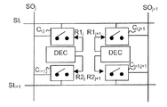
[0020]
According to a particular advantageous embodiment of the invention shown in FIG. 5, the pairs of binary decoders DEC are combined into two pairs of interconnection points. The first pair of interconnection points comprises connection points C i, j and C i + 1, j . The second pair comprises connection points C i, j + 1 and C i + 1, j + 1 . Each decoder DEC always has N inputs (not shown), but in this case the binary decoder has 2 outputs, N for each corresponding pair of two interconnection points. The control signal received through the binary connection path is decoded. Each decoder derives a first result R1 j or R1 j + 1 , each for controlling each pair of first interconnection points. The decoder also comprises inversion means (not shown) which inverts at least one control signal of the N binary connections with respect to the control signal used to derive the first result. . Thus, each decoder obtains a second result R2 j or R2 j + 1 , each controlling a second interconnection point of each pair. For clarity of illustration, both the control connection point and the control member CTRL are not shown in FIG. However, these connections exist for each pair of interconnection points between each decoder DEC and control member CTRL combined into one pair of interconnection points shown in FIG.
[0021]
FIG. 6 shows one embodiment of the decoder DEC shown in FIG. 5, which is shown for illustrative purposes and is a non-limiting example. The decoder is composed of 2-input AND
[0022]
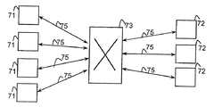
The apparatus shown in FIGS. 1 to 6 is incorporated in an integrated circuit, and can be used particularly for an application in an auto switch of a telecommunications network shown in FIG. FIG. 7 shows an example of a digital telecommunications system according to the present invention. This system includes a
[Brief description of the drawings]
FIG. 1 is a functional diagram showing a configuration example of an apparatus according to a first embodiment of the present invention.
FIG. 2 is a functional diagram showing an example of an apparatus according to a second embodiment of the present invention.
FIG. 3 is a circuit diagram showing a transmission line used in the apparatus according to the present invention.
FIG. 4 is a functional diagram showing an embodiment of a composite element of a device according to the present invention.
FIG. 5 is a functional diagram illustrating a preferred embodiment of an apparatus according to the present invention.
FIG. 6 is a functional diagram showing an embodiment of a local decoder of the device according to the invention.
FIG. 7 is a functional diagram showing a use case of the present invention.
[Explanation of symbols]
10
Claims (9)
前記相互接続点がマトリクスで配置されることにより、2つの別個の伝送路が1つの共通電圧基準経路を備えていることを特徴とするスイッチ装置。A plurality of input ends and output ends connected to each other by an interconnection point matrix controlled by a control member, and an electrical signal is transmitted from the input end to the output end via a transmission line according to a predetermined switching method. In the switching device, each transmission path includes a signal path for transmitting the electrical signal and a reference path to which a predetermined voltage called a voltage reference path is supplied.
A switching device characterized in that the interconnection points are arranged in a matrix so that two separate transmission lines have one common voltage reference path.
また、前記出力端に他の入力端を接続可能なその他の相互接続点のすべては、イナクティブ状態と呼ばれる第2のスイッチング状態に設定され、
前記制御信号を復号し、かつ前記相互接続点のスイッチング状態を導き出すための復号化手段を備え、
前記相互接続点と組み合わされた前記復号化手段が複数の局部デコーダを備えて、前記相互接続点の近傍で前記制御信号を局部的に復号することを特徴とする請求項1から3のいずれか1項に記載のスイッチ装置。A control member that controls the operation of the matrix using a predetermined control signal according to a switching method is provided, and only one output terminal is set to a first switching state called an active state at a predetermined time by the control of the control member. Can be connected to one of the inputs by a specific interconnection point
In addition, all of the other interconnection points that can connect other input terminals to the output terminal are set to a second switching state called an inactive state,
Decoding means for decoding the control signal and deriving a switching state of the interconnection point;
The decoding means combined with the interconnection point comprises a plurality of local decoders, and the control signal is decoded locally in the vicinity of the interconnection point. 2. The switch device according to item 1.
前記2進デコーダは、前記2進制御信号を前記制御部材から前記2進デコーダに送るための伝送路の個別の2進接続路により制御部材に接続され、
制御部材からの個別の2進接続路の数Nが、最大で2Nに等しい複数の相互接続点の数を制御するために設けられていることを特徴とする請求項4に記載のスイッチ装置。The control signal is a binary signal and the decoder is a binary decoder,
The binary decoder is connected to the control member by a separate binary connection of a transmission path for sending the binary control signal from the control member to the binary decoder;
5. Switch device according to claim 4, characterized in that the number N of individual binary connections from the control member is provided for controlling the number of interconnection points equal to at most 2N. .
同一伝送路により同一出力端に接続可能な、相互接続点の対当りN個の入力端及び2つの出力端を有し、相互接続点の前記対に対するN個の2進接続路上で受け取る制御信号を復号し、前記対の第1の相互接続点を制御するための第1の結果を導き出す2進デコーダと、
前記第1の結果を導き出すのに使用された制御信号に関するデコーダで受け取られるN個の2進接続路の少なくとも1つの制御信号を反転し、かつ前記対の第2の相互接続点を制御するための第2の結果を導き出す反転手段とを備えている請求項5に記載のスイッチ装置。The decoding means comprises:
A control signal having N input terminals and two output terminals per pair of interconnection points connectable to the same output terminal by the same transmission line and received on N binary connection paths for the pair of interconnection points And a binary decoder for deriving a first result for controlling the first interconnection point of the pair;
To invert at least one control signal of the N binary connections received at the decoder for the control signal used to derive the first result and to control the second interconnection point of the pair The switch device according to claim 5, further comprising a reversing unit for deriving the second result of
Applications Claiming Priority (2)
| Application Number | Priority Date | Filing Date | Title |
|---|---|---|---|
| FR0115975A FR2833449A1 (en) | 2001-12-11 | 2001-12-11 | High digital transmission rate switching circuit, for optical communication, having interconnection matrix controlled signal and reference transmissions and two distinct lines having common voltage reference channel |
| FR0115975 | 2001-12-11 |
Publications (2)
| Publication Number | Publication Date |
|---|---|
| JP2003229885A JP2003229885A (en) | 2003-08-15 |
| JP4087236B2 true JP4087236B2 (en) | 2008-05-21 |
Family
ID=8870323
Family Applications (1)
| Application Number | Title | Priority Date | Filing Date |
|---|---|---|---|
| JP2002355006A Expired - Fee Related JP4087236B2 (en) | 2001-12-11 | 2002-12-06 | Switch device, integrated circuit, digital transmission system, and auto switch |
Country Status (5)
| Country | Link |
|---|---|
| US (1) | US7245606B2 (en) |
| EP (1) | EP1320227A3 (en) |
| JP (1) | JP4087236B2 (en) |
| CN (1) | CN1314244C (en) |
| FR (1) | FR2833449A1 (en) |
Families Citing this family (2)
| Publication number | Priority date | Publication date | Assignee | Title |
|---|---|---|---|---|
| FR2833441A1 (en) * | 2001-12-11 | 2003-06-13 | Koninkl Philips Electronics Nv | Optical transmission rate packet switching mechanism having matrix function control system and decoder finding switching states with local decoder interconnection point level signal control providing. |
| CN101621507B (en) * | 2008-07-02 | 2012-06-13 | 鸿富锦精密工业(深圳)有限公司 | Dual net physical isolation circuit |
Family Cites Families (10)
| Publication number | Priority date | Publication date | Assignee | Title |
|---|---|---|---|---|
| JPS56153832A (en) * | 1980-04-30 | 1981-11-28 | Nec Corp | Digital to analog converter |
| US4374384A (en) * | 1980-08-28 | 1983-02-15 | Westinghouse Electric Corp. | Matrix encoder for resistive sensor arrays |
| CA1254981A (en) * | 1986-02-18 | 1989-05-30 | Lester Kirkland | Communications switching system |
| USRE34444E (en) * | 1988-01-13 | 1993-11-16 | Xilinx, Inc. | Programmable logic device |
| GB2273627B (en) * | 1990-11-15 | 1996-03-27 | Nvision Inc | Switch composed of identical switch modules |
| KR970009405B1 (en) * | 1991-10-05 | 1997-06-13 | Fujitsu Ltd | Active matrix type display device |
| JPH05199255A (en) * | 1992-01-18 | 1993-08-06 | Mitsubishi Electric Corp | Electronic cross point switch device |
| US5991296A (en) * | 1996-02-22 | 1999-11-23 | Fujitsu, Ltd. | Crossbar switch and method with reduced voltage swing and no internal blocking data path |
| JP3391374B2 (en) * | 1998-12-25 | 2003-03-31 | 富士通株式会社 | Crosspoint switch circuit and basic switch cell electronics |
| FR2833441A1 (en) * | 2001-12-11 | 2003-06-13 | Koninkl Philips Electronics Nv | Optical transmission rate packet switching mechanism having matrix function control system and decoder finding switching states with local decoder interconnection point level signal control providing. |
-
2001
- 2001-12-11 FR FR0115975A patent/FR2833449A1/en not_active Withdrawn
-
2002
- 2002-12-05 EP EP02080091A patent/EP1320227A3/en not_active Withdrawn
- 2002-12-06 US US10/313,786 patent/US7245606B2/en not_active Expired - Fee Related
- 2002-12-06 JP JP2002355006A patent/JP4087236B2/en not_active Expired - Fee Related
- 2002-12-06 CN CNB02154042XA patent/CN1314244C/en not_active Expired - Fee Related
Also Published As
| Publication number | Publication date |
|---|---|
| CN1426205A (en) | 2003-06-25 |
| US20030118032A1 (en) | 2003-06-26 |
| FR2833449A1 (en) | 2003-06-13 |
| EP1320227A3 (en) | 2010-12-08 |
| CN1314244C (en) | 2007-05-02 |
| US7245606B2 (en) | 2007-07-17 |
| JP2003229885A (en) | 2003-08-15 |
| EP1320227A2 (en) | 2003-06-18 |
Similar Documents
| Publication | Publication Date | Title |
|---|---|---|
| US7890680B2 (en) | Physical layer device having a serdes pass through mode | |
| JPH06196958A (en) | Programmable variable length delay circuit | |
| JPH0817502B2 (en) | Network and method for forming modified version of given network | |
| US5559890A (en) | Crypto equipment | |
| CN115065358B (en) | IO driving circuit and chip | |
| CN101009542B (en) | Extension device of data network node device port | |
| JP4087236B2 (en) | Switch device, integrated circuit, digital transmission system, and auto switch | |
| JP4161021B2 (en) | Switch device, integrated circuit, digital transmission system, and auto switch | |
| JPH10190709A (en) | Device system and communication method | |
| TWI746358B (en) | Configurable input/output device and operation method thereof | |
| CN107844672B (en) | Clock tree unit, clock network structure and FPGA clock structure | |
| US8959251B2 (en) | Implementation of switches in a communication network | |
| US8547134B1 (en) | Architecture for high speed serial transmitter | |
| KR20010039467A (en) | N-way switchable power combiner having matched transmission lines according to the number of combined channels | |
| JP2005323297A (en) | 4x4 SWITCH AND 8x8 SWITCH | |
| KR20100063522A (en) | Plc positioning system | |
| JP2575023B2 (en) | Switch matrix | |
| JP2000152293A (en) | Two-way optical transmitter, optical cross connector and optical network system | |
| JPH05167598A (en) | High speed lan light transmission line detour system | |
| JP3675228B2 (en) | Data communication system | |
| JPH03241945A (en) | Cross connector | |
| JPH0468630A (en) | Self-routing network | |
| JP2001016289A (en) | Array transmission circuit and array reception circuit for parallel optical signal transmission | |
| JPH02234535A (en) | Node switch for optical loop | |
| JP2000069052A (en) | Method and device for controlling flow |
Legal Events
| Date | Code | Title | Description |
|---|---|---|---|
| A621 | Written request for application examination |
Free format text: JAPANESE INTERMEDIATE CODE: A621 Effective date: 20051205 |
|
| A977 | Report on retrieval |
Free format text: JAPANESE INTERMEDIATE CODE: A971007 Effective date: 20080121 |
|
| TRDD | Decision of grant or rejection written | ||
| A01 | Written decision to grant a patent or to grant a registration (utility model) |
Free format text: JAPANESE INTERMEDIATE CODE: A01 Effective date: 20080125 |
|
| A61 | First payment of annual fees (during grant procedure) |
Free format text: JAPANESE INTERMEDIATE CODE: A61 Effective date: 20080220 |
|
| FPAY | Renewal fee payment (event date is renewal date of database) |
Free format text: PAYMENT UNTIL: 20110228 Year of fee payment: 3 |
|
| R150 | Certificate of patent or registration of utility model |
Free format text: JAPANESE INTERMEDIATE CODE: R150 |
|
| FPAY | Renewal fee payment (event date is renewal date of database) |
Free format text: PAYMENT UNTIL: 20110228 Year of fee payment: 3 |
|
| S111 | Request for change of ownership or part of ownership |
Free format text: JAPANESE INTERMEDIATE CODE: R313113 |
|
| FPAY | Renewal fee payment (event date is renewal date of database) |
Free format text: PAYMENT UNTIL: 20110228 Year of fee payment: 3 |
|
| R350 | Written notification of registration of transfer |
Free format text: JAPANESE INTERMEDIATE CODE: R350 |
|
| FPAY | Renewal fee payment (event date is renewal date of database) |
Free format text: PAYMENT UNTIL: 20110228 Year of fee payment: 3 |
|
| FPAY | Renewal fee payment (event date is renewal date of database) |
Free format text: PAYMENT UNTIL: 20120229 Year of fee payment: 4 |
|
| FPAY | Renewal fee payment (event date is renewal date of database) |
Free format text: PAYMENT UNTIL: 20130228 Year of fee payment: 5 |
|
| FPAY | Renewal fee payment (event date is renewal date of database) |
Free format text: PAYMENT UNTIL: 20130228 Year of fee payment: 5 |
|
| FPAY | Renewal fee payment (event date is renewal date of database) |
Free format text: PAYMENT UNTIL: 20140228 Year of fee payment: 6 |
|
| R250 | Receipt of annual fees |
Free format text: JAPANESE INTERMEDIATE CODE: R250 |
|
| LAPS | Cancellation because of no payment of annual fees |