EP1320227A2 - Switching device comprising a reference channel with a common voltage - Google Patents
Switching device comprising a reference channel with a common voltage Download PDFInfo
- Publication number
- EP1320227A2 EP1320227A2 EP02080091A EP02080091A EP1320227A2 EP 1320227 A2 EP1320227 A2 EP 1320227A2 EP 02080091 A EP02080091 A EP 02080091A EP 02080091 A EP02080091 A EP 02080091A EP 1320227 A2 EP1320227 A2 EP 1320227A2
- Authority
- EP
- European Patent Office
- Prior art keywords
- interconnection
- control
- points
- matrix
- switching
- Prior art date
- Legal status (The legal status is an assumption and is not a legal conclusion. Google has not performed a legal analysis and makes no representation as to the accuracy of the status listed.)
- Withdrawn
Links
Images


Classifications
-
- H—ELECTRICITY
- H04—ELECTRIC COMMUNICATION TECHNIQUE
- H04L—TRANSMISSION OF DIGITAL INFORMATION, e.g. TELEGRAPHIC COMMUNICATION
- H04L49/00—Packet switching elements
- H04L49/35—Switches specially adapted for specific applications
- H04L49/356—Switches specially adapted for specific applications for storage area networks
- H04L49/357—Fibre channel switches
-
- H—ELECTRICITY
- H04—ELECTRIC COMMUNICATION TECHNIQUE
- H04L—TRANSMISSION OF DIGITAL INFORMATION, e.g. TELEGRAPHIC COMMUNICATION
- H04L49/00—Packet switching elements
- H04L49/10—Packet switching elements characterised by the switching fabric construction
- H04L49/101—Packet switching elements characterised by the switching fabric construction using crossbar or matrix
Definitions
- the invention relates to integrated circuits dedicated to high-speed transmissions. debit.
- a switching device comprising a plurality of inputs and outputs linked together by a matrix of interconnection points controlled by a control unit to transmit electrical signals emitted on said inputs to said outputs via transmission lines according to a plan of predefined switching, each transmission line comprising a signal channel for transport said electrical signals and a reference channel subjected to a voltage given, called voltage reference channel.
- the invention also relates to an integrated circuit comprising such a device. She also relates to a digital transmission system comprising a automatic switch incorporating a switching device for connecting a plurality transmitter and receiver between them. Finally, it relates to an automatic branch exchange digital transmission system.
- the invention has numerous applications, in particular in optical link transmissions. It is particularly advantageous in high speed packet switching applications.
- Integrated circuits used in optical transmissions carry electrical signals at high bit rates, for example of the order of ten Gigabits per second.
- the connections between the inputs and outputs of the circuit suffer significant online losses that have a detrimental effect on circuit performance. Any reduction in the size of the circuit and therefore in the number and the length of these links contributes to improving the performance of the circuit by reducing the losses online.
- These effects are even more remarkable in broadband applications, because the transmission lines are crossed by high frequency currents, this which produces a particular effect, known as a skin effect, increasing the resistivity of the materials used.
- the European patent published under the number EP 1 014 625 describes a device of the kind mentioned in the introductory paragraph intended to optimize the relationship between the size of the switching matrix and its capacity in number of inputs and of outputs.
- the device comprises a plurality of switching cells arranged in cascade to form a multi-stage matrix network in which each cell of switching has two inputs and two outputs.
- the cells are interconnected in cascade over multiple levels or switching stages so that any input of any cell can be switched to any output of another cell any, via one or more switching stages, according to the interconnection plan of the matrix.
- the multistage switching matrix as provided for in the patent cited above is relatively complex to make and order because there is no connection single direct between all the inputs and all the outputs of the matrix.
- An object of the invention is to provide a switching device having a reduced footprint for high speed applications, which is more efficient and more simple to make and to control than the device described in the patent already cited.
- the invention modify the arrangement of the different components of the matrix to reuse certain components already present by adapting them so as to obtain, due to the repetition of these components in the matrix, a notable reduction in the total space occupied by the matrix.
- the points interconnection points are arranged in pairs of interconnection points so that two adjacent pairs have a common voltage reference channel.
- the control member is designed to control the operation of the matrix by means of control signals predetermined according to the switching plan, so that at a given time, an output does not can be connected to only one of said inputs by a single interconnection point placed in a first switching state, called active state, under the control of the control. All other interconnection points likely to connect other inputs on said output being placed in a second switching state, said inactive state. of the decoding means are provided for decoding said control signals and for deduce the switching state of said interconnection points.
- the decoding means comprise a plurality of decoders associated with the points interconnection to effect local decoding of said control signals at the level said interconnection points. The local decoding of the control signals makes it possible to reduce the number of control links required between the control body and the points interconnection, which reduces the space occupied by these control links.
- the two interconnection points forming said pair being connectable to the same output of the matrix.
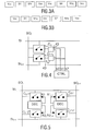
- Figure 1 shows an example of a switching device according to the invention. It comprises a rectangle matrix 10, of type nxm, n representing the number of inputs, denoted I 0 to I n , and m the number of outputs from the matrix, denoted O 0 to O m . Each input and each output is connected to a separate transmission line.
- the transmission lines are interconnected at interconnection points forming matrix switching cells, denoted C 00 to C nm , the first index referring to the index of the input I 0 to I n and the second index referring to the index of the corresponding output O 0 to O m .
- Each transmission line with index i or j, at the input or output of the matrix consists of a signal channel, denoted SI i or SO j , respectively, for transporting an electrical signal from an input I i or to an output O j of the matrix and of a reference channel, denoted Vcc, subjected to a reference voltage, for example the supply voltage Vcc at 2.5 Volts.
- the voltage reference channel Vcc can, for example, serve as a return channel for the signal transmitted on the corresponding signal channel S j . It can also have other uses, and serve, in particular, as electromagnetic shielding and / or supply path.
- the function of the interconnection points or switching cells C i, j is to switch the signal channel SI i corresponding to the input I i to the signal channel SO j corresponding to the output O j .
- the interconnection points are represented in FIG. 1 by simple two-state switches.
- the type of switch used to exercise the function of the interconnection points is not limited to the switch C i, j shown in FIG. 1.
- the signal channels are represented by a line simple.
- each signal channel may consist of two separate parallel differential channels. The principle of the invention as described with reference to all the figures remains valid in the case of differential transmission lines.
- the interconnection points C i, j are arranged in the matrix so that two separate transmission lines have a common voltage reference path Vcc.
- the switching cells C 0.0 and C 1.0 on the one hand and C 2.0 and C 3.0 on the other hand, connectable to the same output transmission line, SO 0 are grouped in pairs so that the transmission lines corresponding to the two entries of the matrix of successive indices I 1 and I 2 , are arranged side by side.
- a single voltage reference channel Vcc is provided between the corresponding signal channels SI 1 and SI 2 .
- This voltage reference channel can, in particular, serve as a return channel common to the two signal channels SI 1 and SI 2 .
- interconnection points are grouped into complex cells 22 of four points interconnection, so that two adjacent cells 22 have a reference channel in common tension.
- Figure 2 shows only part of the switching matrix with four adjacent complex cells.
- the principle of the invention is applied in the two dimensions of the matrix, at the level of input and output transmission lines.
- the same elements have the same reference as in Figure 1.
- the pooling of a reference channel Vcc is here between two transmission lines connected to two successive outputs as well as between two transmission lines connected to two successive inputs of the matrix.
- This configuration in complex cells of 4 interconnection points saves space a reference channel as well as a space between lines, for each complex cell, in the two dimensions of the matrix.
- Figure 3A is a schematic sectional representation of a pair of transmission lines which can be used in a switching matrix.
- the signals conveyed in optical transmissions are signals differential in phase opposition. That is, a signal line of one line transmission is actually made up of two parallel differential components for carry the differential signal.
- the principle of the matrix described with reference to the figures previous is kept, except that a signal channel actually consists of two channels parallel differentials.
- Each transmission line therefore has two channels differential S and Sq to transport the signal and a voltage reference channel or channel back Vcc.
- the total congestion resulting for a pair of successive differential transmission lines arranged according to FIG. 3A corresponds to 4 (A + B + B ') + 2A' + C.
- FIG. 3B illustrates a pair of differential transmission lines arranged according to the invention as illustrated, for example, in Figures 1 and 2.
- the same references are used to indicate the same elements.
- the voltage reference channel Vcc is common to the two successive differential transmission lines, which allows reduce the overall size of the two transmission lines. Indeed, using the same notations as for FIG. 3A, a total bulk of 4A + 2A '+ 3B + 4B', i.e. a reduction equal to B + C.
- the space saving achieved by the removal of a voltage reference channel per pair of transmission lines is estimated at minus about 10% of the space used according to each dimension of the matrix.
- FIG. 4 illustrates a part of a device according to a particular embodiment of the invention.
- Half of a complex cell 22 illustrated in FIG. 2 is represented in FIG. 4. This half corresponding to two interconnection points or basic cells C i, j and C i + 1, j associated with the same line of output transmission.
- a control member CTRL is provided for controlling the operation of the matrix by means of predetermined control signals according to said predefined switching plan.
- an output can only be connected to a single input by a single interconnection point placed in a first switching state, called active state, under the control of the control unit CTRL, all the others interconnection points capable of connecting other inputs to this same output being placed in a second switching state, called inactive state.
- Decoding means 43 are provided for decoding the control signals and deducing therefrom the switching state of the interconnection points.
- the decoding means 43 include local decoders associated with the interconnection points to perform local decoding of the control signals sent by the control member at the interconnection points.
- the control signals are binary signals and the decoders 43, binary decoders.
- the binary decoders 43 are connected to the control member by binary links distinct from the transmission lines to transport the binary control signals from the CTRL control member to the binary decoders 43.
- a pair of binary decoders DEC is associated with two pairs of interconnection points.
- the first pair of points comprises the points C i, j and C i + 1, j .
- the second pair has the points C i, j + 1 and C i + 1, j + 1 .
- each DEC decoder always has N inputs (not shown) but this time the binary decoders have 2 outputs for decoding the control signals received on the N binary links to the 2 interconnection points of each corresponding pair.
- Each decoder deduces therefrom a first result R1 j and R1 j + 1 , respectively, intended to control the first interconnection point of each pair.
- the decoders further include inverting means (not shown) for inverting the control signal on at least one of the N bit links with respect to the control signal used to provide the first result.
- Each decoder thus obtains a second result R2 j and R2 j + 1 , respectively, intended to control the second interconnection point of the corresponding pair.
- neither the control links nor the CTRL control member are shown in FIG. 5. These links are however present for each pair of interconnection points, between each DEC decoder associated with a pair of interconnection points and the CTRL control unit, as illustrated in Figure 4.
- FIG. 6 illustrates, purely by way of non-restrictive example, an embodiment of a DEC decoder represented in FIG. 5.
- the decoder comprises two stages of AND logic gates, denoted 61 to 63, for connecting 3 inputs, denoted b0 , b1 and b2, with two outputs, denoted S0 and S1.
- the 3 inputs b0, b1 and b2 are connected to the control device (not shown) via the N control links illustrated in Figure 4.
- the 2 outputs S0 and S1 are intended to provide the two binary control results , R1 j or R1 j + 1 on the one hand, and R2 j or R2 j + 1 on the other hand, to control a pair of interconnection points C i, j and C i + 1, j or C i, j + 1 and C i + 1, j + 1 , connectable, via a transmission line, to the same output of the switching matrix, O j or O j + 1 , according to the example illustrated in Figure 5.
- Two inputs b0 and b1 are connected to the input of a first AND gate 61 whose output is sent to the input of a second and third AND gate 62 and 63, respectively.
- the third input b2 is received at the input of the second AND gate 62 to provide, by performing a logical AND with the output of the first AND gate 61, a first command result R1 intended for the first interconnection point C i, j .
- Inversion means 65 are provided for inverting the signal received on the third input b2 and for supplying at the input of the third AND gate 63 said inverted signal with respect to the signal sent at the input of the second AND gate 62 and for deducing therefrom, by performing a logical AND with the output of the first AND gate 61, the second command result R2 intended for the second interconnection point C i + 1, j .
- FIGS. 4 to 6 which are not made to scale, such a DEC decoder with two outputs as illustrated in FIGS. 5 and 6 is less bulky than the sum of the two decoders 43 shown in Figure 4.
- FIGS. 1 to 6 can be incorporated in a integrated circuit, to be used, in particular, in a PABX of a network of telecommunications as shown in Figure 7.
- Figure 7 shows an example of digital telecommunications system according to the invention.
- the system includes a transmitter 71, receiver 72, automatic switch 73 comprising a device for switching of the type represented in FIGS. 1 to 5 and of the connections by optical fibers 75 to connect the transmitter 71 and the receiver 72 via the automatic exchange 73.
Abstract
Description
L'invention concerne les circuits intégrés dédiés aux transmissions à haut débit. En particulier, elle concerne un dispositif de commutation comportant une pluralité d'entrées et de sorties reliées entre elles par une matrice de points d'interconnexion commandée par un organe de contrôle pour transmettre des signaux électriques émis sur lesdites entrées vers lesdites sorties via des lignes de transmission selon un plan de commutation prédéfini, chaque ligne de transmission comportant une voie de signal pour transporter lesdits signaux électriques et une voie de référence soumise à une tension donnée, dite voie de référence en tension.The invention relates to integrated circuits dedicated to high-speed transmissions. debit. In particular, it relates to a switching device comprising a plurality of inputs and outputs linked together by a matrix of interconnection points controlled by a control unit to transmit electrical signals emitted on said inputs to said outputs via transmission lines according to a plan of predefined switching, each transmission line comprising a signal channel for transport said electrical signals and a reference channel subjected to a voltage given, called voltage reference channel.
L'invention concerne aussi un circuit intégré comportant un tel dispositif. Elle concerne également un système de transmissions numériques comportant un autocommutateur incorporant un dispositif de commutation pour relier une pluralité d'émetteur et de récepteurs entre eux. Elle concerne enfin un autocommutateur d'un système de transmissions numériques.The invention also relates to an integrated circuit comprising such a device. She also relates to a digital transmission system comprising a automatic switch incorporating a switching device for connecting a plurality transmitter and receiver between them. Finally, it relates to an automatic branch exchange digital transmission system.
L'invention a de nombreuses applications notamment dans les systèmes de transmissions par liaisons optiques. Elle est particulièrement avantageuse dans les applications de commutation de paquets à haut débit.The invention has numerous applications, in particular in optical link transmissions. It is particularly advantageous in high speed packet switching applications.
Les circuits intégrés utilisés dans les transmissions optiques véhiculent des signaux électriques à des débits élevés, par exemple de l'ordre d'une dizaine de Gigabits par seconde. A ces vitesses de transmission, les liaisons entre les entrées et les sorties du circuit subissent des pertes en ligne non négligeables qui ont une influence néfaste sur les performances du circuit. Toute réduction de la taille du circuit et donc du nombre et de la longueur de ces liaisons contribue à améliorer les performances du circuit en diminuant les pertes en ligne. Ces effets sont encore plus remarquables dans les applications à haut débit, du fait que les lignes de transmission sont traversées par des courants à haute fréquence, ce qui produit un effet particulier, connu sous le nom d'effet de peau, augmentant la résistivité des matériaux utilisés.Integrated circuits used in optical transmissions carry electrical signals at high bit rates, for example of the order of ten Gigabits per second. At these transmission speeds, the connections between the inputs and outputs of the circuit suffer significant online losses that have a detrimental effect on circuit performance. Any reduction in the size of the circuit and therefore in the number and the length of these links contributes to improving the performance of the circuit by reducing the losses online. These effects are even more remarkable in broadband applications, because the transmission lines are crossed by high frequency currents, this which produces a particular effect, known as a skin effect, increasing the resistivity of the materials used.
Le brevet européen publié sous le numéro EP 1 014 625 décrit un dispositif
de commutation du genre mentionné dans le paragraphe introductif destiné à optimiser le
rapport entre la taille de la matrice de commutation et sa capacité en nombre d'entrées et
de sorties. Le dispositif comporte une pluralité de cellules de commutation arrangées en
cascade pour former un réseau matriciel multi-étages dans lequel chaque cellule de
commutation comporte deux entrées et deux sorties. Les cellules sont interconnectées en
cascade sur plusieurs niveaux ou étages de commutation de manière à ce que toute entrée
d'une cellule quelconque puisse être commutée sur toute sortie d'une autre cellule
quelconque, via un ou plusieurs étages de commutation, selon le plan d'interconnexion de la
matrice. La matrice de commutation multi-étages tel que prévu dans le brevet cité ci-dessus
est relativement complexe à réaliser et à commander du fait qu'il n'existe pas de liaison
unique directe entre toutes les entrées et toutes les sorties de la matrice. La réalisation, le
contrôle et la programmation d'une telle matrice, lorsqu'elle est utilisée, par exemple, dans
des applications de commutation de paquets à haut débit, est assez complexe à mettre en
oeuvre. De plus, la construction d'une telle matrice en cascades de plusieurs étages est
préjudiciable pour les performances du circuit, notamment en terme de gigue.The European patent published under the
Un objet de l'invention est de fournir un dispositif de commutation ayant un encombrement réduit pour des applications à haut débit, qui soit plus performant et plus simple à réaliser et à commander que le dispositif décrit dans le brevet déjà cité. L'invention modifie l'agencement des différents composants de la matrice pour réutiliser certains composants déjà présents en les adaptant de manière à obtenir, du fait de la répétition de ces composants dans la matrice, une réduction notable de l'espace total occupé par la matrice.An object of the invention is to provide a switching device having a reduced footprint for high speed applications, which is more efficient and more simple to make and to control than the device described in the patent already cited. The invention modify the arrangement of the different components of the matrix to reuse certain components already present by adapting them so as to obtain, due to the repetition of these components in the matrix, a notable reduction in the total space occupied by the matrix.
Pour cela, il est prévu un dispositif du genre mentionné dans le paragraphe introductif remarquable en ce que les points d'interconnexion sont arrangés dans la matrice de sorte que deux lignes de transmission distinctes comportent une voie de référence en tension commune. Cette configuration permet d'économiser au moins l'espace occupé par une voie de référence en tension autant de fois qu'il y a de paires de sorties dans la matrice.For this, a device of the kind mentioned in the paragraph is provided. remarkable introduction in that the interconnection points are arranged in the matrix so that two separate transmission lines have a reference channel in common tension. This configuration saves at least the space occupied by a voltage reference channel as many times as there are pairs of outputs in the matrix.
Selon un mode de réalisation particulier, il est prévu que les points d'interconnexion sont arrangés en paires de points d'interconnexion de sorte que deux paires adjacentes aient une voie de référence en tension commune.According to a particular embodiment, it is expected that the points interconnection points are arranged in pairs of interconnection points so that two adjacent pairs have a common voltage reference channel.
Selon un autre mode de réalisation de l'invention, l'organe de contrôle est prévu pour contrôler le fonctionnement de la matrice au moyen de signaux de contrôle prédéterminés selon le plan de commutation, de sorte qu'à un instant donné, une sortie ne puisse être connectée qu'à une seule desdites entrées par un point d'interconnexion unique placé dans un premier état de commutation, dit état actif, sous la commande de l'organe de contrôle. Tous les autres points d'interconnexion susceptibles de connecter d'autres entrées sur ladite sortie étant placés dans un deuxième état de commutation, dit état inactif. Des moyens de décodage sont prévus pour décoder lesdits signaux de contrôle et pour en déduire l'état de commutation desdits points d'interconnexion. Selon ce mode de réalisation, les moyens de décodage comportent une pluralité de décodeurs associés aux points d'interconnexion pour effectuer un décodage local desdits signaux de contrôle au niveau desdits points d'interconnexion. Le décodage local des signaux de contrôle permet de réduire le nombre de liaisons de contrôle nécessaires entre l'organe de contrôle et les points d'interconnexion, ce qui diminue d'autant l'espace occupé par ces liaisons de contrôle.According to another embodiment of the invention, the control member is designed to control the operation of the matrix by means of control signals predetermined according to the switching plan, so that at a given time, an output does not can be connected to only one of said inputs by a single interconnection point placed in a first switching state, called active state, under the control of the control. All other interconnection points likely to connect other inputs on said output being placed in a second switching state, said inactive state. of the decoding means are provided for decoding said control signals and for deduce the switching state of said interconnection points. According to this embodiment, the decoding means comprise a plurality of decoders associated with the points interconnection to effect local decoding of said control signals at the level said interconnection points. The local decoding of the control signals makes it possible to reduce the number of control links required between the control body and the points interconnection, which reduces the space occupied by these control links.
Selon encore un autre mode de réalisation de l'invention, il est prévu d'utiliser un seul décodeur local ayant 2 sorties, associé à des moyens d'inversion, par paire de points d'interconnexion d'une même cellule complexe, le décodeur unique étant plus simple et plus petit que la somme des décodeurs utilisés selon l'ancienne configuration. Les deux points d'interconnexion formant ladite paire étant connectables à une même sortie de la matrice. Ce qui revient à utiliser une seule paire de décodeurs par cellule complexe de quatre points d'interconnexion au lieu de 4 décodeurs (un par point d'interconnexion). L'espace utilisé par les deux décodeurs supprimés peut alors être économisé.According to yet another embodiment of the invention, provision is made to use a single local decoder having 2 outputs, associated with reversing means, per pair interconnection points of the same complex cell, the single decoder being more simple and smaller than the sum of the decoders used according to the old configuration. The two interconnection points forming said pair being connectable to the same output of the matrix. This amounts to using a single pair of decoders per complex cell of four interconnection points instead of 4 decoders (one per interconnection point). The space used by the two deleted decoders can then be saved.
Les modes de réalisation suivants, donnés à titre d'exemples non limitatifs pour illustrer comment l'invention peut être réalisée, sont décrits en regard des dessins ci-annexés, parmi lesquels :
- la figure 1 est un schéma fonctionnel pour illustrer un exemple de dispositif selon un premier mode de réalisation de l'invention,
- la figure 2 est un schéma fonctionnel pour illustrer un exemple de dispositif selon un deuxième mode de réalisation de l'invention,
- la figure 3 est un schéma de principe pour illustrer une ligne de transmission utilisée dans un dispositif selon l'invention,
- la figure 4 est un schéma fonctionnel pour illustrer un exemple de réalisation d'une cellule complexe d'un dispositif selon l'invention,
- la figure 5 est un schéma fonctionnel pour illustrer un exemple de réalisation préféré d'un dispositif selon l'invention,
- la figure 6 est un schéma fonctionnel pour illustrer un exemple de réalisation d'un décodeur local dans un dispositif selon l'invention,
- la figure 7 est un schéma fonctionnel pour illustrer un exemple d'application de l'invention.
- FIG. 1 is a functional diagram to illustrate an example of a device according to a first embodiment of the invention,
- FIG. 2 is a functional diagram to illustrate an example of a device according to a second embodiment of the invention,
- FIG. 3 is a block diagram to illustrate a transmission line used in a device according to the invention,
- FIG. 4 is a functional diagram to illustrate an exemplary embodiment of a complex cell of a device according to the invention,
- FIG. 5 is a functional diagram to illustrate a preferred embodiment of a device according to the invention,
- FIG. 6 is a functional diagram to illustrate an exemplary embodiment of a local decoder in a device according to the invention,
- Figure 7 is a block diagram to illustrate an example of application of the invention.
La figure 1 montre un exemple de dispositif de commutation selon
l'invention. Il comporte une matrice rectangle 10, de type n x m, n représentant le nombre
d'entrées, notées I0 à In, et m le nombre de sorties de la matrice, notées O0 à Om. Chaque
entrée et chaque sortie sont reliées à une ligne de transmission distincte. Les lignes de
transmission sont interconnectées au niveau de points d'interconnexion formant des cellules
de commutation de la matrice, notés C00 à Cnm, le premier indice faisant référence à l'indice
de l'entrée I0 à In et le deuxième indice faisant référence à l'indice de la sortie
correspondante O0 à Om. Chaque ligne de transmission d'indice i ou j, en entrée ou en sortie
de la matrice, se compose d'une voie de signal, notée SIi ou SOj, respectivement, pour
transporter un signal électrique depuis une entrée Ii ou vers une sortie Oj de la matrice et
d'une voie de référence, notée Vcc, soumise à une tension de référence, par exemple la
tension d'alimentation Vcc à 2,5 Volts. La voie de référence en tension Vcc peut, par
exemple, servir de voie de retour au signal transmis sur la voie de signal Sj correspondante.
Elle peut également avoir d'autres usages, et servir, notamment, comme blindage
électromagnétique et/ou voie d'alimentation. Les points d'interconnexion ou cellules de
commutation Ci,j ont pour fonction de commuter la voie de signal SIi correspondant à l'entrée
Ii sur la voie de signal SOj correspondant à la sortie Oj. Pour simplifier, les points
d'interconnexion sont représentés sur la figure 1 par des commutateurs simples à deux
états. Mais le type de commutateur utilisé pour exercer la fonction des points
d'interconnexion n'est pas limité au commutateur Ci,j représenté sur la figure 1. Dans le
même but de simplification des figures, les voies de signal sont représentées par une ligne
simple. Pour des applications de transmissions optiques, chaque voie de signal peut être
constituée de deux voies différentielles parallèles distinctes. Le principe de l'invention tel que
décrit en référence à toutes les figures reste valable dans le cas de lignes de transmission
différentielles.Figure 1 shows an example of a switching device according to the invention. It comprises a
Selon ce principe, les points d'interconnexion Ci,j sont arrangés dans la matrice de sorte que deux lignes de transmission distinctes comportent une voie de référence en tension commune Vcc. Dans la figure 1, les cellules de commutation C0,0 et C1,0 d'une part et C2,0 et C3,0 d'autre part, connectables à une même ligne de transmission de sortie, SO0, sont regroupées par paires de façon à ce que les lignes de transmission correspondant aux deux entrées de la matrice d'indices successifs I1 et I2, soient disposées côte à côte. Une seule et même voie de référence en tension Vcc est prévue entre les voies de signal correspondantes SI1 et SI2. Cette voie de référence en tension peut, notamment, servir de voie de retour commune aux deux voies de signal SI1 et SI2. Cela permet d'économiser la place nécessaire pour une voie de référence ainsi que la place d'un espace entre lignes à chaque fois que deux paires de points d'interconnexion sont ainsi associées. La même configuration peut être reproduite au niveau des lignes de transmission correspondant aux entrées suivantes, par exemple, en utilisant une voie de référence en tension commune pour les lignes de transmissions correspondant aux entrées I3 et I4, puis I5 et I6 et ainsi de suite Le même principe s'applique également dans l'autre dimension de la matrice en regroupant par paires des points d'interconnexion du type Ci,j et Ci,j+1 d'une part et Ci,j+2 et Ci,j+3 d'autre part, connectables à une même ligne de transmission d'entrée de type SIi et à des sorties d'indices successifs SOj et SOj+1 d'une part et SOj+2 et SOj+3, d'autre part. According to this principle, the interconnection points C i, j are arranged in the matrix so that two separate transmission lines have a common voltage reference path Vcc. In FIG. 1, the switching cells C 0.0 and C 1.0 on the one hand and C 2.0 and C 3.0 on the other hand, connectable to the same output transmission line, SO 0 , are grouped in pairs so that the transmission lines corresponding to the two entries of the matrix of successive indices I 1 and I 2 , are arranged side by side. A single voltage reference channel Vcc is provided between the corresponding signal channels SI 1 and SI 2 . This voltage reference channel can, in particular, serve as a return channel common to the two signal channels SI 1 and SI 2 . This saves the space necessary for a reference channel as well as the space of a space between lines each time two pairs of interconnection points are thus associated. The same configuration can be reproduced at the level of the transmission lines corresponding to the following inputs, for example, by using a common voltage reference channel for the transmission lines corresponding to the inputs I3 and I4, then I5 and I6 and so on. same principle also applies in the other dimension of the matrix by grouping in pairs interconnection points of the type C i, j and C i, j + 1 on the one hand and C i, j + 2 and C i , j + 3 on the other hand, connectable to the same input transmission line of type SI i and to outputs of successive indices SO j and SO j + 1 on the one hand and SO j + 2 and SO j +3 , on the other hand.
Selon un mode de réalisation préféré de l'invention schématisé à la figure 2,
les points d'interconnexion sont regroupés en cellules complexes 22 de quatre points
d'interconnexion, de sorte que deux cellules adjacentes 22 ont une voie de référence en
tension commune. La figure 2 ne représente qu'une partie de la matrice de commutation
comportant quatre cellules complexes adjacentes. Selon ce mode de réalisation avantageux,
le principe de l'invention est appliqué dans les deux dimensions de la matrice, au niveau des
lignes de transmission d'entrée et de sortie. Les mêmes éléments portent les mêmes
référence que sur la figure 1. La mise en commun d'une voie de référence Vcc est ici
réalisée entre deux lignes de transmission reliées à deux sorties successives ainsi qu'entre
deux lignes de transmission reliées à deux entrées successives de la matrice. Cette
configuration en cellules complexes de 4 points d'interconnexion permet de gagner la place
d'une voie de référence ainsi qu'un espace entre lignes, pour chaque cellule complexe, dans
les deux dimensions de la matrice.According to a preferred embodiment of the invention shown diagrammatically in FIG. 2,
interconnection points are grouped into
La figure 3A est une représentation schématique en coupe d'une paire de lignes de transmission pouvant être utilisées dans une matrice de commutation. Comme déjà mentionné, les signaux véhiculés dans les transmissions optiques sont des signaux différentiels en opposition de phase. C'est-à-dire qu'une voie de signal d'une ligne de transmission est en fait constituée de deux composantes différentielles parallèles pour transporter le signal différentiel. Le principe de la matrice décrit en référence aux figures précédentes est conservé, sauf qu'une voie de signal est en réalité constituée de deux voies différentielles parallèles. Chaque ligne de transmission comporte donc deux voies différentielles S et Sq pour transporter le signal et une voie de référence en tension ou voie de retour Vcc. En notant A l'espace occupé par une composante d'une voie de signal différentiel, B l'espace occupé par une voie de référence en tension Vcc, A' l'espace entre deux voies de signal, B' l'espace entre une voie de signal et une voie de référence en tension et C l'espace entre deux voies de référence en tension, l'encombrement total résultant pour une paire de lignes de transmission différentielles successives agencées selon la figure 3A correspond à 4(A+B+B')+2A'+C.Figure 3A is a schematic sectional representation of a pair of transmission lines which can be used in a switching matrix. As already mentioned, the signals conveyed in optical transmissions are signals differential in phase opposition. That is, a signal line of one line transmission is actually made up of two parallel differential components for carry the differential signal. The principle of the matrix described with reference to the figures previous is kept, except that a signal channel actually consists of two channels parallel differentials. Each transmission line therefore has two channels differential S and Sq to transport the signal and a voltage reference channel or channel back Vcc. By noting A the space occupied by a component of a signal channel differential, B the space occupied by a reference channel in voltage Vcc, A 'the space between two signal channels, B 'the space between a signal channel and a voltage reference channel and C the space between two voltage reference channels, the total congestion resulting for a pair of successive differential transmission lines arranged according to FIG. 3A corresponds to 4 (A + B + B ') + 2A' + C.
La figure 3B illustre une paire de lignes de transmission différentielles arrangées selon l'invention telle qu'illustrée, par exemple, aux figures 1 et 2. Les mêmes références sont utilisées pour indiquer les mêmes éléments. La voie de référence en tension Vcc est commune aux deux lignes de transmission différentielles successives, ce qui permet de réduire l'encombrement total des deux lignes de transmission. En effet, en utilisant les mêmes notations que pour la figure 3A, on obtient un encombrement total de 4A+2A'+3B+4B', soit une réduction égale à B+C. Le gain de place réalisé par la suppression d'une voie de référence en tension par paire de lignes de transmission est estimée à au moins environ 10 % de l'espace utilisé selon chaque dimension de la matrice. Figure 3B illustrates a pair of differential transmission lines arranged according to the invention as illustrated, for example, in Figures 1 and 2. The same references are used to indicate the same elements. The voltage reference channel Vcc is common to the two successive differential transmission lines, which allows reduce the overall size of the two transmission lines. Indeed, using the same notations as for FIG. 3A, a total bulk of 4A + 2A '+ 3B + 4B', i.e. a reduction equal to B + C. The space saving achieved by the removal of a voltage reference channel per pair of transmission lines is estimated at minus about 10% of the space used according to each dimension of the matrix.
La figure 4 illustre une partie d'un dispositif selon un mode de réalisation
particulier de l'invention. La moitié d'une cellule complexe 22 illustrée à la figure 2 est
représenté sur la figure 4. Cette moitié correspondant à deux points d'interconnexion ou
cellules de base Ci,j et Ci+1,j associés à une même ligne de transmission en sortie. Un organe
de contrôle CTRL est prévu pour contrôler le fonctionnement de la matrice au moyen de
signaux de contrôle prédéterminés selon ledit plan de commutation prédéfini. A un instant
donné, une sortie ne peut être connectée qu'à une seule entrée par un point
d'interconnexion unique placé dans un premier état de commutation, dit état actif, sous la
commande de l'organe de contrôle CTRL, tous les autres points d'interconnexion
susceptibles de connecter d'autres entrées sur cette même sortie étant placés dans un
deuxième état de commutation, dit état inactif. Des moyens de décodage 43 sont prévus
pour décoder les signaux de contrôle et en déduire l'état de commutation des points
d'interconnexion. Les moyens de décodage 43 comportent des décodeurs locaux associés
aux points d'interconnexion pour réaliser un décodage local des signaux de contrôle envoyés
par l'organe de contrôle au niveau des points d'interconnexion. Dans l'exemple illustré, les
signaux de contrôle sont des signaux binaires et les décodeurs 43, des décodeurs binaires.
Les décodeurs binaires 43 sont reliés à l'organe de contrôle par des liaisons binaires
distinctes des lignes de transmission pour transporter les signaux de contrôle binaires depuis
l'organe de contrôle CTRL jusqu'aux décodeurs binaires 43. Dans l'exemple illustré à la figure
4, un nombre N de liaisons binaires distinctes partant de l'organe de contrôle sont prévues
pour contrôler un nombre de points d'interconnexion égal au maximum à 2N. Dans cet
exemple, N=3.FIG. 4 illustrates a part of a device according to a particular embodiment of the invention. Half of a
Selon un mode de réalisation particulièrement avantageux de l'invention illustré à la figure 5, une paire de décodeurs binaires DEC est associée à deux paires de points d'interconnexion. La première paire de points comporte les points Ci,j et Ci+1,j. La deuxième paire comporte les points Ci,j+1 et Ci+1,j+1. chaque décodeur DEC comporte toujours N entrées (non représentées) mais cette fois les décodeurs binaires comportent 2 sorties pour décoder les signaux de contrôle reçus sur les N liaisons binaires à destination des 2 points d'interconnexion de chaque paire correspondante. Chaque décodeur en déduit un premier résultat R1j et R1j+1, respectivement, destiné à commander le premier point d'interconnexion de chaque paire. Les décodeurs comportent en outre des moyens d'inversion (non représentés) pour inverser le signal de contrôle sur au moins l'une des N liaisons binaires par rapport au signal de contrôle utilisé pour fournir le premier résultat. Chaque décodeur obtient ainsi un deuxième résultat R2j et R2j+1, respectivement, destiné à commander le deuxième point d'interconnexion de la paire correspondante. Pour des raisons de clarté des figures, ni les liaisons de contrôle ni l'organe de contrôle CTRL ne sont représentés sur la figure 5. Ces liaisons sont cependant présentes pour chaque paire de points d'interconnexion, entre chaque décodeur DEC associé à une paire de points d'interconnexion et l'organe de contrôle CTRL, tel qu'illustré à la figure 4.According to a particularly advantageous embodiment of the invention illustrated in FIG. 5, a pair of binary decoders DEC is associated with two pairs of interconnection points. The first pair of points comprises the points C i, j and C i + 1, j . The second pair has the points C i, j + 1 and C i + 1, j + 1 . each DEC decoder always has N inputs (not shown) but this time the binary decoders have 2 outputs for decoding the control signals received on the N binary links to the 2 interconnection points of each corresponding pair. Each decoder deduces therefrom a first result R1 j and R1 j + 1 , respectively, intended to control the first interconnection point of each pair. The decoders further include inverting means (not shown) for inverting the control signal on at least one of the N bit links with respect to the control signal used to provide the first result. Each decoder thus obtains a second result R2 j and R2 j + 1 , respectively, intended to control the second interconnection point of the corresponding pair. For reasons of clarity of the figures, neither the control links nor the CTRL control member are shown in FIG. 5. These links are however present for each pair of interconnection points, between each DEC decoder associated with a pair of interconnection points and the CTRL control unit, as illustrated in Figure 4.
La figure 6 illustre, à titre purement indicatif et non restrictif, un exemple de
réalisation d'un décodeur DEC représenté à la figure 5. Le décodeur comporte deux étages
de portes logiques ET, notées 61 à 63, pour relier 3 entrées, notées b0, b1 et b2, à deux
sorties, notées S0 et S1. Les 3 entrées b0, b1 et b2, sont reliées à l'organe de contrôle (non
représenté) via les N liaisons de contrôle illustrées à la figure 4. Les 2 sorties S0 et S1, sont
destinées à fournir les deux résultats de commande binaires, R1j ou R1j+1 d'une part, et R2j
ou R2j+1 d'autre part, pour commander une paire de points d'interconnexion Ci,j et Ci+1,j ou
Ci,j+1 et Ci+1,j+1, connectable, via une ligne de transmission, à une même sortie de la matrice
de commutation, Oj ou Oj+1, selon l'exemple illustré à la figure 5. Deux entrées b0 et b1 sont
connectées en entrée d'une première porte ET 61 dont la sortie est envoyée en entrée d'une
deuxième et d'une troisième porte ET 62 et 63, respectivement. La troisième entrée b2 est
reçue en entrée de la deuxième porte ET 62 pour fournir, en réalisant un ET logique avec la
sortie de la première porte ET 61, un premier résultat de commande R1 à destination du
premier point d'interconnexion Ci,j. Des moyens d'inversion 65 sont prévus pour inverser le
signal reçu sur la troisième entrée b2 et pour fournir en entrée de la troisième porte ET 63
ledit signal inversé par rapport au signal envoyé en entrée de la deuxième porte ET 62 et
pour en déduire, en réalisant un ET logique avec la sortie de la première porte ET 61, le
deuxième résultat de commande R2 à destination du deuxième point d'interconnexion Ci+1,j.
Bien que cela n'apparaisse pas sur les figures 4 à 6 qui ne sont pas réalisées à l'échelle, un
tel décodeur DEC à deux sorties tel qu'illustré aux figures 5 et 6 est moins encombrant que
la somme des deux décodeurs 43 représentés à la figure 4.FIG. 6 illustrates, purely by way of non-restrictive example, an embodiment of a DEC decoder represented in FIG. 5. The decoder comprises two stages of AND logic gates, denoted 61 to 63, for connecting 3 inputs, denoted b0 , b1 and b2, with two outputs, denoted S0 and S1. The 3 inputs b0, b1 and b2, are connected to the control device (not shown) via the N control links illustrated in Figure 4. The 2 outputs S0 and S1, are intended to provide the two binary control results , R1 j or R1 j + 1 on the one hand, and R2 j or R2 j + 1 on the other hand, to control a pair of interconnection points C i, j and C i + 1, j or C i, j + 1 and C i + 1, j + 1 , connectable, via a transmission line, to the same output of the switching matrix, O j or O j + 1 , according to the example illustrated in Figure 5. Two inputs b0 and b1 are connected to the input of a first AND
Un dispositif tel qu'illustré sur les figures 1 à 6 peut être incorporé dans un
circuit intégré, pour être utilisé, notamment, dans un autocommutateur d'un réseau de
télécommunications tel que représenté sur la figure 7. La figure 7 représente un exemple de
système de télécommunications numériques selon l'invention. Le système comporte un
émetteur 71, un récepteur 72, un autocommutateur 73 comportant un dispositif de
commutation du type représenté aux figures 1 à 5 et des liaisons par fibres optiques 75
pour relier l'émetteur 71 et le récepteur 72 via l'autocommutateur 73.A device as illustrated in FIGS. 1 to 6 can be incorporated in a
integrated circuit, to be used, in particular, in a PABX of a network of
telecommunications as shown in Figure 7. Figure 7 shows an example of
digital telecommunications system according to the invention. The system includes a
Claims (9)
Applications Claiming Priority (2)
| Application Number | Priority Date | Filing Date | Title |
|---|---|---|---|
| FR0115975A FR2833449A1 (en) | 2001-12-11 | 2001-12-11 | High digital transmission rate switching circuit, for optical communication, having interconnection matrix controlled signal and reference transmissions and two distinct lines having common voltage reference channel |
| FR0115975 | 2001-12-11 |
Publications (2)
| Publication Number | Publication Date |
|---|---|
| EP1320227A2 true EP1320227A2 (en) | 2003-06-18 |
| EP1320227A3 EP1320227A3 (en) | 2010-12-08 |
Family
ID=8870323
Family Applications (1)
| Application Number | Title | Priority Date | Filing Date |
|---|---|---|---|
| EP02080091A Withdrawn EP1320227A3 (en) | 2001-12-11 | 2002-12-05 | Switching device comprising a reference channel with a common voltage |
Country Status (5)
| Country | Link |
|---|---|
| US (1) | US7245606B2 (en) |
| EP (1) | EP1320227A3 (en) |
| JP (1) | JP4087236B2 (en) |
| CN (1) | CN1314244C (en) |
| FR (1) | FR2833449A1 (en) |
Families Citing this family (2)
| Publication number | Priority date | Publication date | Assignee | Title |
|---|---|---|---|---|
| FR2833441A1 (en) * | 2001-12-11 | 2003-06-13 | Koninkl Philips Electronics Nv | Optical transmission rate packet switching mechanism having matrix function control system and decoder finding switching states with local decoder interconnection point level signal control providing. |
| CN101621507B (en) * | 2008-07-02 | 2012-06-13 | 鸿富锦精密工业(深圳)有限公司 | Dual net physical isolation circuit |
Citations (1)
| Publication number | Priority date | Publication date | Assignee | Title |
|---|---|---|---|---|
| EP1014625A2 (en) * | 1998-12-25 | 2000-06-28 | Fujitsu Limited | Crosspoint switch circuit and switch cell electronic circuit |
Family Cites Families (9)
| Publication number | Priority date | Publication date | Assignee | Title |
|---|---|---|---|---|
| JPS56153832A (en) * | 1980-04-30 | 1981-11-28 | Nec Corp | Digital to analog converter |
| US4374384A (en) * | 1980-08-28 | 1983-02-15 | Westinghouse Electric Corp. | Matrix encoder for resistive sensor arrays |
| CA1254981A (en) * | 1986-02-18 | 1989-05-30 | Lester Kirkland | Communications switching system |
| USRE34444E (en) * | 1988-01-13 | 1993-11-16 | Xilinx, Inc. | Programmable logic device |
| GB2273627B (en) * | 1990-11-15 | 1996-03-27 | Nvision Inc | Switch composed of identical switch modules |
| KR970009405B1 (en) * | 1991-10-05 | 1997-06-13 | Fujitsu Ltd | Active matrix type display device |
| JPH05199255A (en) * | 1992-01-18 | 1993-08-06 | Mitsubishi Electric Corp | Electronic cross point switch device |
| US5991296A (en) * | 1996-02-22 | 1999-11-23 | Fujitsu, Ltd. | Crossbar switch and method with reduced voltage swing and no internal blocking data path |
| FR2833441A1 (en) * | 2001-12-11 | 2003-06-13 | Koninkl Philips Electronics Nv | Optical transmission rate packet switching mechanism having matrix function control system and decoder finding switching states with local decoder interconnection point level signal control providing. |
-
2001
- 2001-12-11 FR FR0115975A patent/FR2833449A1/en not_active Withdrawn
-
2002
- 2002-12-05 EP EP02080091A patent/EP1320227A3/en not_active Withdrawn
- 2002-12-06 CN CNB02154042XA patent/CN1314244C/en not_active Expired - Fee Related
- 2002-12-06 JP JP2002355006A patent/JP4087236B2/en not_active Expired - Fee Related
- 2002-12-06 US US10/313,786 patent/US7245606B2/en not_active Expired - Fee Related
Patent Citations (1)
| Publication number | Priority date | Publication date | Assignee | Title |
|---|---|---|---|---|
| EP1014625A2 (en) * | 1998-12-25 | 2000-06-28 | Fujitsu Limited | Crosspoint switch circuit and switch cell electronic circuit |
Non-Patent Citations (1)
| Title |
|---|
| 160 GBIT/S HIGH SPEED ATM SWITCHING SYSTEM: "160 GBIT/S HIGH SPEED ATM SWITCHING SYSTEM" NTT REVIEW, TELECOMMUNICATIONS ASSOCIATION, TOKYO, JP, vol. 9, no. 2, 1 mars 1997 (1997-03-01), pages 28-35, XP000687064 ISSN: 0915-2334 * |
Also Published As
| Publication number | Publication date |
|---|---|
| EP1320227A3 (en) | 2010-12-08 |
| CN1426205A (en) | 2003-06-25 |
| CN1314244C (en) | 2007-05-02 |
| JP2003229885A (en) | 2003-08-15 |
| FR2833449A1 (en) | 2003-06-13 |
| US20030118032A1 (en) | 2003-06-26 |
| JP4087236B2 (en) | 2008-05-21 |
| US7245606B2 (en) | 2007-07-17 |
Similar Documents
| Publication | Publication Date | Title |
|---|---|---|
| EP0817408B1 (en) | Receiver for optical digital signal transmission system | |
| CA2235058C (en) | Surface acoustic wave device with proximity coupling and differential input/outputs | |
| EP0711093A1 (en) | Switching system for optical packets | |
| EP0497670B1 (en) | Optical concentrator | |
| EP3534536B1 (en) | Photonic device and method for dual band frequency conversion | |
| FR2898223A1 (en) | CIRCUIT FOR DISTRIBUTING AN INITIAL SIGNAL WITH A SHAFT STRUCTURE PROTECTED AGAINST LOGICAL ALEAS. | |
| EP1646262A1 (en) | A reconfigurable optical switch | |
| EP0905907B1 (en) | Exclusive OR gate with four two by two complementary inputs and two complementary outputs and frequency multiplier using the same | |
| EP1320227A2 (en) | Switching device comprising a reference channel with a common voltage | |
| EP1322076A1 (en) | Switching device with means for local decoding | |
| FR2796766A1 (en) | Optical bi-directional amplifier for fibre optics has two pumping sources with output applied to fibre optic via multiplexers | |
| EP1179964A2 (en) | Optical signal switch | |
| EP1349417B1 (en) | Multicasting optical cross-connect | |
| FR2830709A1 (en) | Reconfigurable optical switching system for frequency division multiplex system, includes optical switches to selectively and respectively connect output port of demultiplexer to input port of multiplexer | |
| FR2729040A1 (en) | PHOTONIC SWITCH MATRIX | |
| EP1497939A1 (en) | Optical device and method of converting wdm signals into an otdm signal and vice versa | |
| FR2814305A1 (en) | WAVELENGTH SELECTION AND CONVERSION DEVICE, AND THE INCORPORATED PHOTONIC SWITCHING MATRIX | |
| FR2821504A1 (en) | FREQUENCY EXTRACTION DEVICE | |
| FR2743965A1 (en) | PASSIVE ROUTING OPTICAL COMMUNICATION METHOD AND SYSTEM | |
| EP1544669A1 (en) | optical signal regenerator, use of such a device and system including such a device | |
| FR2709839A1 (en) | Switch for switching optical signals | |
| FR2734920A1 (en) | METHOD AND DEVICE FOR COMBINING OPTICAL SIGNALS | |
| EP1326473A1 (en) | Optical switching device and control method therefor | |
| FR2819665A1 (en) | PHOTON SWITCHING DEVICE | |
| EP1314267A1 (en) | All-optical regenerator for wavelength-division multiplexed signals |
Legal Events
| Date | Code | Title | Description |
|---|---|---|---|
| PUAI | Public reference made under article 153(3) epc to a published international application that has entered the european phase |
Free format text: ORIGINAL CODE: 0009012 |
|
| AK | Designated contracting states |
Designated state(s): AT BE BG CH CY CZ DE DK EE ES FI FR GB GR IE IT LI LU MC NL PT SE SI SK TR |
|
| AX | Request for extension of the european patent |
Extension state: AL LT LV MK RO |
|
| RAP1 | Party data changed (applicant data changed or rights of an application transferred) |
Owner name: NXP B.V. |
|
| PUAL | Search report despatched |
Free format text: ORIGINAL CODE: 0009013 |
|
| AK | Designated contracting states |
Kind code of ref document: A3 Designated state(s): AT BE BG CH CY CZ DE DK EE ES FI FR GB GR IE IT LI LU MC NL PT SE SI SK TR |
|
| AX | Request for extension of the european patent |
Extension state: AL LT LV MK RO |
|
| AKY | No designation fees paid | ||
| REG | Reference to a national code |
Ref country code: DE Ref legal event code: R108 |
|
| REG | Reference to a national code |
Ref country code: DE Ref legal event code: R108 Effective date: 20110822 |
|
| STAA | Information on the status of an ep patent application or granted ep patent |
Free format text: STATUS: THE APPLICATION IS DEEMED TO BE WITHDRAWN |
|
| 18D | Application deemed to be withdrawn |
Effective date: 20110609 |