JP4079552B2 - Nonvolatile semiconductor memory that prevents unauthorized copying - Google Patents
Nonvolatile semiconductor memory that prevents unauthorized copying Download PDFInfo
- Publication number
- JP4079552B2 JP4079552B2 JP20335799A JP20335799A JP4079552B2 JP 4079552 B2 JP4079552 B2 JP 4079552B2 JP 20335799 A JP20335799 A JP 20335799A JP 20335799 A JP20335799 A JP 20335799A JP 4079552 B2 JP4079552 B2 JP 4079552B2
- Authority
- JP
- Japan
- Prior art keywords
- storage area
- read
- state
- write
- signal
- Prior art date
- Legal status (The legal status is an assumption and is not a legal conclusion. Google has not performed a legal analysis and makes no representation as to the accuracy of the status listed.)
- Expired - Fee Related
Links
Images


Classifications
-
- G—PHYSICS
- G11—INFORMATION STORAGE
- G11C—STATIC STORES
- G11C16/00—Erasable programmable read-only memories
-
- G—PHYSICS
- G11—INFORMATION STORAGE
- G11C—STATIC STORES
- G11C16/00—Erasable programmable read-only memories
- G11C16/02—Erasable programmable read-only memories electrically programmable
- G11C16/06—Auxiliary circuits, e.g. for writing into memory
- G11C16/22—Safety or protection circuits preventing unauthorised or accidental access to memory cells
Landscapes
- Engineering & Computer Science (AREA)
- Computer Security & Cryptography (AREA)
- Storage Device Security (AREA)
- Read Only Memory (AREA)
Description
【0001】
【発明の属する技術分野】
本発明は、主記憶領域に記憶されたデータを不正に複写されることを防止したフラッシュメモリなどの不揮発性半導体メモリに関する。
【0002】
【従来の技術】
不揮発性の半導体メモリであるフラッシュメモリは、電気的にデータの書き込み(プログラム)及び消去を行うことができ、電源オフにしても記録されたデータが失われないことから広く利用されている。例えば、インターネットを通じて有料で配信した音楽データを記録するメモリカードとして、普及しつつある。また、携帯電話など小型携帯情報端末の特定のデータやプログラムを記憶するメモリとしても広く利用されるようになっている。
【0003】
上記のフラッシュメモリに記録した音楽データや特定データ若しくはプログラムが、不正にコピーされたり、フラッシュメモリが不正に入手した情報機器に利用されたりすることを防止するために、不正コピー防止機能や不正使用防止機能が要求されている。これらの機能は、例えば、フラッシュメモリ内に通常のデータを記録する主記憶領域に加えて、特殊なデータやキーコードを記録する隠し記憶領域を設けることで実現される。この隠し記憶領域は、ワンタイム・プログラマブルメモリであり、通常のユーザは使用できない記憶領域である。
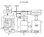
【0004】
図1は、不正コピー防止と不正コピーとを説明する為の図である。フラッシュメモリには、通常のデータを記録する主記憶領域1と、特殊なデータを記録する隠し記憶領域2とが設けられ、更に、隠し記憶領域2内に記録されたデータの書き換えを禁止する書き込みプロテクト回路3が設けられる。それ以外に、フラッシュメモリには、書き込み(プログラム)、消去、読み出しのために必要な回路が内蔵される。
【0005】
今仮に、フラッシュメモリA,Bは正当に市場で入手されたメモリであり、フラッシュメモリXは不正に入手されたメモリであるとする。正当に市場に出されたフラッシュメモリA,Bには、それぞれの隠し記憶領域2にキーコードA,Bが書き込まれ、それぞれの書き込みプロテクト回路3は、書き換えを禁止するプロテクト状態にされている。そして、例えば、フラッシュメモリAに所定の音楽データAが記録される場合は、キーコードAに従ってデータAが暗号化され、その暗号化されたデータAが主記憶領域1に記録される。そして、音楽データAを再生する時は、データAが読み出され、キーコードAによって復号化され、その復号化された音楽データAが再生される。
【0006】
一方、不正に音楽データAをフラッシュメモリBに複写した場合は、フラッシュメモリBの主記憶領域1内には、キーコードAで暗号化されたデータAがコピーされることになる。従って、不正にコピーした音楽データAを再生しようとしても、フラッシュメモリBの隠し記憶領域2内のキーコードBで復号化されて元の音楽データAを取得することはできず、結局再生することができない。
【0007】
音楽データの変わりに、特殊なデータやプログラムの場合でも同じ手法で不正コピーによる情報の不正利用を防止することができる。
【0008】
【発明が解決しようとする課題】
しかしながら、仮に、出荷段階で隠し記憶領域2内にキーコードが書き込まれていない状態のフラッシュメモリXが、不正に闇市場に出回った場合は、上記の不正コピー防止機能が損なわれてしまう。即ち、正当な暗号化されたデータAを記憶したフラッシュメモリAから、隠し記憶領域2内のキーコードAと、主記憶領域1内の暗号化されたデータAの両方を、不正に入手したフラッシュメモリXのそれぞれの領域1,2に記録することで、データAを不正にコピーして不正に利用することが可能になる。
【0009】
従って、上記のように特殊コードが書き込まれないまま不正に闇市場に出回った場合でも、データの不正コピーとそれに伴うデータの不正利用を防止することができる不揮発性半導体メモリが求められる。
【0010】
そこで、本発明の目的は、データの不正コピーを防止することができる不揮発性半導体メモリを提供することにある。
【0011】
更に、本発明の目的は、不正に闇市場に出回った場合でも、データの不正コピーとそれに伴うデータの不正利用を防止することができる不揮発性半導体メモリを提供することにある。
【0012】
【課題を解決するための手段】
上記の目的を達成するために、本発明の一つの側面は、不揮発性の半導体メモリにおいて、通常のデータを記録する主記憶領域に加えて、不正コピーを防止するための特殊コードを記録する隠し記憶領域を有し、この隠し記憶領域は、書き込みプロテクト状態の時は読み出し許可状態にあり、書き込みプロテクト状態ではない時は読み出し禁止状態にある。従って、半導体メモリのベンダーが隠し記憶領域に特殊コードを記録し書き込みプロテクト状態にして初めて、隠し記憶領域を読み出すことが可能になる。そして、この書き込みプロテクト状態への変更方法は、ベンダー以外には秘密になっている。その結果、隠し記憶領域に特殊コードが記録されていない半導体メモリを、闇市場で不正に入手しても、隠し記憶領域の読み出しが禁止されたままであるので、不正コピーしたデータを利用することができず、結果的に不正コピーが防止される。
【0013】
上記の目的を達成するために、本発明の別の側面は、不揮発性の半導体メモリにおいて、通常のデータを記録する主記憶領域に加えて、不正コピーを防止するための特殊コードを記録する隠し記憶領域を有し、この隠し記憶領域は、上記特殊コードが記録されて初めて読み出し許可状態になるように構成されている。従って、半導体メモリのベンダーが隠し記憶領域に特殊コードを記録して初めて、隠し記憶領域を読み出すことが可能になり、上記と同様に不正コピーが防止される。
【0014】
上記の特殊コードは、例えば主記憶領域のデータを暗号化するための暗号化コード若しくはその暗号化コードを生成するためのコードである。または、特殊コードは、その半導体メモリが使用できる情報機器とのマッチングをとるための認識コードの場合もある。この特殊コードを利用することにより、主記憶領域内のデータが不正に別のメモリにコピーされても、そのコピーされたデータの利用ができないようにすることができる。
【0015】
上記の目的を達成するために、本発明の一つの側面は、電気的にデータの書き込み及び読み出しを行う不揮発性の半導体メモリにおいて、
通常のデータを記録する主記憶領域と、不正コピーを防止するための特殊コードを記録する隠し記憶領域と、前記隠し記憶領域を書き込みプロテクト状態にする書き込みプロテクト回路とを有し、
前記隠し記憶領域は、書き込みプロテクト状態の時は読み出し許可状態にあり、書き込みプロテクト状態ではない時は読み出し禁止状態にあることを特徴とする。
【0016】
上記の発明の好ましい実施例は、更に、外部からの書き込み及び読み出しコマンドをデコードし、前記隠し記憶領域に対する内部書き込み信号及び内部読み出し信号をそれぞれ生成するコマンドデコーダを有し、
前記コマンドデコーダは、前記書き込みプロテクト回路が書き込みプロテクト状態でない時は、前記内部読み出し信号の生成を禁止され、書き込みプロテクト状態の時は、前記内部読み出し信号の生成を許可されることを特徴とする。
【0017】
本発明の別の側面は、電気的にデータの書き込み及び読み出しを行う不揮発性の半導体メモリにおいて、
通常のデータを記録する主記憶領域と、不正コピーを防止するための特殊コードを記録する隠し記憶領域とを有し、
前記隠し記憶領域は、前記特殊コードが記録されていない時は読み出し禁止状態にあり、前記特殊コードが記録されている時は読み出し許可状態にあることを特徴とする。
【0018】
上記の発明のより好ましい実施例は、更に、前記隠し記憶領域を書き込みプロテクト状態にする書き込みプロテクト回路と、前記隠し記憶領域を読み出しプロテクト状態にする読み出しプロテクト回路とを有し、前記読み出しプロテクト回路が読み出しプロテクト状態の時は、前記隠し記憶領域の読み出しが禁止され、読み出しプロテクト状態でない時は、前記隠し記憶領域の読み出しが許可されることを特徴とする。
【0019】
【発明の実施の形態】
以下、図面を参照して本発明の実施の形態例を説明する。しかしながら、かかる実施の形態例が、本発明の技術的範囲を限定するものではない。
【0020】
図1に従って、本発明の実施の形態例を説明する。本実施の形態例では、隠し記憶領域2を書き込みからプロテクトする書き込みプロテクト回路3が、書き込みプロテクト状態でない時は、隠し記憶領域2の読み出しを禁止し、隠し記憶領域2に特殊コードが書き込まれて書き込みプロテクト状態にされた時に初めて読み出しが許可される。即ち、書き込みプロテクト回路3の書き込みプロテクト状態と、隠し記憶領域2の読み出し禁止状態とを連動させることで、隠し記憶領域2に特殊コードが書き込まれていないフラッシュメモリは、その隠し記憶領域2の読み出しができないようにする。従って、隠し記憶領域2への書き込みがなされていないフラッシュメモリが、不正に入手されたとしても、隠し記憶領域2の読み出しができないので、不正コピーされたデータが利用されることが防止される。
【0021】
図2は、第1の実施の形態例におけるフラッシュメモリの構成図である。図2のフラッシュメモリでは、通常のデータを記憶する主記憶領域1と、特殊コードを記録する隠し記憶領域(ヒデゥン・ブロック、Hidden Block)2とを有し、これらの記憶領域1,2内には、フローティングゲートを有する不揮発性メモリトランジスタが複数設けられる。
【0022】
主記憶領域1内のワード線はロウ・デコーダ24により選択され、隠し記憶領域2内のワード線は対応するデコーダ25により選択される。両記憶領域1,2に設けられたビット線は、コラムゲート27を介してセンスアンプ18に接続される。コラムゲート27は、コラムデコーダ26により選択される。ロウ・デコーダ24には、アドレス12が供給されるプリデコーダ23からプリデコード信号が供給される。
【0023】
隠し記憶領域2は、例えば主記憶領域1内のブロック領域と同等の容量を有し、制御回路30からの選択信号SELにより選択される。また、主記憶領域1は、制御回路30からの選択信号/SELにより選択される。
【0024】
外部からの入出力データは、入出力回路20に供給されると共に入出力回路20から出力される。入出力回路20とセンスアンプ18とはデータバスを介して接続される。図2のメモリには、フラッシュメモリに特有のコマンドデコーダ22が設けられる。コマンドデコーダ22は、入出力データ端子から入出力回路20に供給された特定のコマンドをデコードし、種々の内部動作制御信号S1,S2,S3、PTprgmを生成する。この内部動作制御信号S1,S2,S3は、コマンドデコーダ22が生成する内部動作制御信号の一部であり、これらの内部動作制御信号については、後で説明する。
【0025】
書き込みプロテクト回路3は、後述する通り、隠し記憶領域2の書き込みを禁止する書き込みプロテクト状態を記憶する記憶回路を有し、その記憶状態に応じて、書き込みプロテクト信号PTを出力する。この書き込みプロテクト信号PTが活性化状態であると、コマンドデコーダ22による、隠し記憶領域2への内部書き込み信号S3、内部消去信号S2の生成が禁止され、隠し記憶領域2に記録されている特殊コードの書き換えが禁止される。
【0026】
この書き込みプロテクト回路3の記憶回路は、外部から供給される秘密のコマンドに応答してコマンドデコーダ22が発生するプロテクト・プログラム信号PTprgmにより、書き込みプロテクト状態にされる。そして、一旦書き込みプロテクト状態にされると、書き込みプロテクト信号PTが活性化状態になり、コマンドデコーダ22によるプロテクト・プログラム信号PTPrgmの生成が禁止され、書き込みプロテクト回路3の記憶回路を再度非プロテクト状態にすることはできない。
【0027】
第1の実施の形態例で特徴的なところは、書き込みプロテクト回路3が書き込みプロテクト状態ではないと、コマンドデコーダ22による隠し記憶領域2を読み出すための内部読み出し信号S1の生成が禁止され、書き込みプロテクト状態になると、当該内部読み出し信号S1の生成が許可されることにある。従って、隠し記憶領域2への特殊コードの書き込みが行われる前の初期状態では、書き込みプロテクト回路3が書き込みプロテクト状態になっていないので、隠し記憶領域2に特殊コードを書き込んでも、それを読み出すことは禁止される。従って、不正コピーしたデータを利用することはできない。
【0028】
図3は、主記憶領域と隠し記憶領域の詳細構成図である。主記憶領域1と隠し記憶領域2とは、複数のワード線WL0,WL1,WLnと、複数のビット線BL0,BL1と、それらの交差位置に設けられるフローティングゲートを有する不揮発性メモリトランジスタからなるメモリセルMC00〜MCn1とを有する。メモリセルのドレインはビット線に接続され、コントロールゲートはワード線に接続され、ソースはソース線SLに接続される。ソース線SLは、ソース線電圧制御回路19に接続される。それ以外の構成は、図2に示した通りであり、同じ引用番号が与えられる。
【0029】
図4は、コマンドデコーダの構成例を示す図である。図4の例では、隠れ記憶領域2の読み出しを行う内部読み出し信号S1と、隠れ記憶領域2の消去を行う内部消去信号S2と、隠れ記憶領域2の書き込み(プログラム)を行う内部プログラム信号S3と、書き込みプロテクト回路3を書き込みプロテクト状態にするプロテクト・プログラム信号PTPrgmとが、それぞれのANDゲートにより生成される。
【0030】
内部読み出し信号S1は、ANDゲート40,41,42によりコマンドDB0〜DB7がデコードされ、ラッチ回路43にラッチされ、インバータ44を介して生成される。内部消去信号S2、内部プログラム信号S3も同様の回路構成により対応するコマンドがデコードされて生成される。プロテクト・プログラム信号PTPrgmは、所定の秘密コードSTが供給されると、ANDゲート55,56によりデコードされ、ラッチ回路57にラッチされ、インバータ58を介して生成される。
【0031】
コマンドデコーダ22には、書き込みプロテクト信号PTが供給され、書き込みプロテクト信号PTが書き込みプロテクト状態でない時(Lレベル)に、ANDゲート42により内部読み出し信号S1の生成が禁止される。その状態の時に、書き込みプロテクト信号PTはインバータ60で反転され、その反転信号/PTのHレベルにより、隠れ記憶領域2に対する内部消去信号S2、内部プログラム信号S3の生成が許可される。また、反転信号/PTのHレベルにより、書き込みプロテクト回路3へのプロテクト・プログラム信号PTPrgmの生成が許可される。プロテクト・プログラム信号PTPrgmは、秘密のコードSTの供給に応答して、生成される。従って、通常の利用者には、この書き込みプロテクト状態へのプログラムは不可能である。
【0032】
プロテクト・プログラム信号PTPrgmにより書き込みプロテクト回路3内の記憶回路に書き込みプロテクト状態が書き込まれると、書き込みプロテクト信号PTはHレベルになる。その結果、ANDゲート47,52により、コマンドデコーダ22は、内部消去信号S2、内部プログラム信号S3の生成を禁止され、隠れ記憶領域2へのデータの書き換えは禁止される。また、ANDゲート56により、コマンドデコーダ22は、プロテクト・プログラム信号PTPrgmの生成を禁止され、その後の書き込みプロテクト回路3への書き換えが禁止される。
【0033】
図5は、書き込みプロテクト回路の一例を示す回路図である。書き込みプロテクト回路3内には、書き込みプロテクト状態を記憶する記憶回路61が設けられる。この書き込みプロテクト記憶回路61は、フローティングゲートを有する記憶トランジスタFM1を有し、コントロールゲートは所定の電圧が印加される端子N3に接続され、ソースはグランド電位Vssに接続される。
【0034】
書き込みプロテクト回路3は、ゲートがグランドにバイアスされたPチャネルの負荷トランジスタPTr1と、増幅用のNチャネルトランジスタ62と、NANDゲート63と、インバータ65,66、及びプロテクト・プログラム用のNチャネルトランジスタ64とを有する。トランジスタ64のゲートには、プロテクト・プログラム信号PTPrgmが供給され、NANDゲート63には、その反転信号/PTPrgmとノードN2が供給される。
【0035】
初期状態において、書き込みプロテクト記憶回路61のトランジスタFM1は、フローティングゲートに電子が注入されないで閾値電圧が低い状態にある。その場合は、端子N3に読み出し電圧を印加すると、トランジスタFM1が導通し、ノードN2がLレベルになり、NANDゲート63の出力がHレベルになり、トランジスタ62がより導通し、ノードN1がLレベルになる。従って、書き込みプロテクト信号PTは、非活性状態のLレベルにある。即ち、書き込みプロテクト状態になっていない。
【0036】
この書き込みプロテクト信号PTがLレベルの状態では、前述の通り、コマンドデコーダ22は、外部からのコマンドコードに応答して、内部消去信号S2,内部プログラム信号S3、プロテクト・プログラム信号PTPrgmを生成することを許可される。しかし、内部読み出し信号S1の生成は禁止されている。
【0037】
次に、隠し記憶領域2への特殊コードの書き込みが終了すると、外部から秘密コードSTが供給され、コマンドデコーダ22は、それを検出して、プロテクト・プログラム信号PTPrgmをHレベルにする。その結果、書き込みプロテクト回路3のトランジスタ64が導通し、ノードN1がLレベルに引っ張られる。また、その反転信号/PTPrgmがLレベルになるので、NANDゲート63の出力はHレベルになり、トランジスタ62が導通し、ノードN2もグランド電位Vssにされる。そのとき、ノードN3に高い電圧を印加することで、トランジスタFM1のフローティングゲートに電子が注入され、その閾値電圧が高くなる。特殊コードの書き込みと書き込みプロテクト状態への変換は、一連の工程で行われ、後に書き込んだ特殊データを読み出すことができるようにされる。
【0038】
この状態で、書き込みプロテクト回路3のノードN3に読み出し電圧を印加しても、トランジスタFM1が導通しないので、ノードN2はHレベルのままである。信号/PTPrgmはH レベルになっているので、NANDゲート63の出力はLレベルになり、トランジスタ62は非導通状態になり、ノードN1からその下側のトランジスタFM1が切り離される。従って、ノードN1は、負荷トランジスタPTr1によりHレベルに引き上げられる。従って、書き込みプロテクト信号PTはHレベルの活性化状態になる。
【0039】
この書き込みプロテクト信号PTがHレベルになると、前述の通り、コマンドデコーダ22は、外部からのコマンドコードの供給に対して、内部消去信号S2,内部プログラム信号S3、プロテクト・プログラム信号PTPrgmを生成することを禁止される。従って、隠れ記憶領域2へのデータの書き換えは禁止され、書き込みプロテクト回路3内へのプロテクト状態の解除の書き換えも禁止される。
【0040】
[第2の実施の形態例]
図6は、第2の実施の形態例におけるフラッシュメモリの構成図である。図6には、図2と同じ部分には同じ引用番号を与えている。第2の実施の形態例では、隠し記憶領域2に対する書き込みプロテクト回路3に加えて、隠し記憶領域2のデータの読み出しを禁止するための読み出しプロテクト回路4が設けられる。即ち、書き込みプロテクト状態と読み出しプロテクト状態とは、必ずしも連動しない。
【0041】
読み出しプロテクト回路4の構成は、基本的に図5に示された書き込みプロテクト回路3と同じである。そして、コマンドデコーダ22が外部からの読み出しプロテクトコマンドに応答して生成する読み出しプロテクト・プログラム信号ENPrgmにより、読み出しプロテクト回路4の状態が、読み出し許可状態にされる。具体的には、書き込みプロテクト回路3の場合と同様に、読み出しプロテクト回路4内の記憶回路をプログラムする。
【0042】
それに伴い、読み出しプロテクト信号ENが活性レベル(Hレベル)になり、コマンドデコーダ22による内部読み出し信号S1の生成が許可され、隠し記憶領域2のデータの外部からの読み出しが可能になる。また、読み出しプロテクト信号ENがHレベルになると、コマンドデコーダ22による読み出しプロテクト・プログラム信号ENPrgmの生成が禁止され、読み出しプロテクト回路内の記憶回路の書き換えが禁止される。
【0043】
図7は、第2の実施の形態例におけるコマンドデコーダ22の構成を示す図である。図7には、図4と対応する部分には同じ引用番号を与えている。図7のコマンドデコーダは、図4の構成に加えて、秘密のコードST2をデコードするANDゲート70,71、ラッチ回路72及びインバータ73が設けられ、読み出しプロテクト・プログラム信号ENPrgmが生成される。
【0044】
図7のコマンドデコーダ22は、図4と同様に、書き込みプロテクト信号PTが初期状態のLレベルの時は、インバータ60により反転された信号/PTのHレベルにより、外部供給コマンドに対応して隠し記憶領域2への内部消去信号S2、内部プログラム信号S3、及び書き込みプロテクト回路3に対するプロテクト・プログラム信号PTPrgmの生成は許可される。一方、書き込みプロテクト信号PTが活性状態(Hレベル)になると、インバータ60により反転された信号/PTのLレベルにより、外部供給コマンドに対応して隠し記憶領域2への内部消去信号S2、内部プログラム信号S3、及び書き込みプロテクト回路3に対するプロテクト・プログラム信号PTPrgmの生成が禁止される。
【0045】
更に、図7のコマンドデコーダ22は、読み出しプロテクト信号ENが初期状態の非活性化状態(Lレベル)の時は、ANDゲート42により隠し記憶領域2への内部読み出し信号S1の生成が禁止され、インバータ75による反転信号/ENのHレベルにより、秘密コードST2に対応する読み出しプロテクト・プログラム信号ENPrgmの生成は、許可される。また、読み出しプロテクト信号ENが初期状態の活性化状態(Hレベル)の時は、隠し記憶領域2への内部読み出し信号S1の生成が許可され、インバータ75による反転信号/ENのLレベルにより、秘密コードST2に対応する読み出しプロテクト・プログラム信号ENPrgmの生成は、禁止される。
【0046】
上記のように第2の実施の形態例では、フラッシュメモリのベンダーは、メモリの製造工程では、読み出しプロテクト信号ENは非活性状態(Lレベル)を初期状態にし、隠し記憶領域2への内部読み出し信号S1の生成を禁止し、読み出しができないようにする。そして、試験工程を経て良品になった場合に、その隠し記憶領域2に対して、内部消去信号S2と内部プログラム信号S3を利用して特殊コードを書き込みすると同時に、書き込みプロテクト回路3を書き込みプロテクト状態にすると共に、読み出しプロテクト・プログラム信号ENPrgmを発生させて、読み出しプロテクト回路4内の記憶回路を読み出し許可状態にする。
【0047】
従って、隠し記憶領域2に特殊データが書き込まれていない不正入手のフラッシュメモリでは、隠し記憶領域2のデータを読み出すことができないので、不正にコピーしたデータを利用することが防止される。
【0048】
以上、本発明の保護範囲は、上記の実施の形態例に限定されるものではなく、特許請求の範囲に記載された発明とその均等物にまで及ぶものである。
【0049】
【発明の効果】
以上、本発明によれば、不揮発性半導体メモリにおいて、不正コピー防止用の特殊コードが書き込まれてないメモリを不正に入手されても、コピーされたデータの不正利用を防止することができ、結果的に不正コピーを防止することができる。
【図面の簡単な説明】
【図1】不正コピー防止と不正コピーとを説明する為の図である。
【図2】第1の実施の形態例におけるフラッシュメモリの構成図である。
【図3】主記憶領域と隠し記憶領域の詳細構成図である。
【図4】コマンドデコーダの構成例を示す図である。
【図5】書き込みプロテクト回路の一例を示す回路図である。
【図6】第2の実施の形態例におけるフラッシュメモリの構成図である。
【図7】第2の実施の形態例におけるコマンドデコーダ22の構成を示す図である。
【符号の説明】
1 主記憶領域
2 隠し記憶領域
3 書き込みプロテクト回路
4 読み出しプロテクト回路
22 コマンドデコーダ
PT 書き込みプロテクト信号
EN 読み出しプロテクト信号[0001]
BACKGROUND OF THE INVENTION
The present invention relates to a nonvolatile semiconductor memory such as a flash memory that prevents unauthorized copying of data stored in a main storage area.
[0002]
[Prior art]
A flash memory, which is a non-volatile semiconductor memory, is widely used because it can electrically write (program) and erase data and does not lose recorded data even when the power is turned off. For example, it is becoming popular as a memory card that records music data distributed for a fee through the Internet. In addition, it is widely used as a memory for storing specific data and programs of small portable information terminals such as mobile phones.
[0003]
In order to prevent music data, specific data or programs recorded in the above flash memory from being illegally copied, or being used by information devices from which the flash memory has been illegally obtained, Prevention function is required. These functions are realized, for example, by providing a hidden storage area for recording special data and key codes in addition to a main storage area for recording normal data in the flash memory. This hidden storage area is a one-time programmable memory and cannot be used by a normal user.
[0004]
FIG. 1 is a diagram for explaining illegal copy prevention and illegal copy. The flash memory is provided with a
[0005]
Assume that the flash memories A and B are legally obtained in the market, and the flash memory X is illegally obtained. Key codes A and B are written in the respective
[0006]
On the other hand, when the music data A is illegally copied to the flash memory B, the data A encrypted with the key code A is copied into the
[0007]
In the case of special data and programs instead of music data, it is possible to prevent unauthorized use of information by unauthorized copying using the same technique.
[0008]
[Problems to be solved by the invention]
However, if the flash memory X in which the key code is not written in the
[0009]
Therefore, there is a need for a non-volatile semiconductor memory that can prevent unauthorized copying of data and the accompanying unauthorized use of data even if it is illegally marketed without writing a special code as described above.
[0010]
Accordingly, an object of the present invention is to provide a nonvolatile semiconductor memory capable of preventing illegal copying of data.
[0011]
Furthermore, an object of the present invention is to provide a nonvolatile semiconductor memory capable of preventing unauthorized copying of data and accompanying unauthorized use of data even when illegally on the black market.
[0012]
[Means for Solving the Problems]
To achieve the above object, according to one aspect of the present invention, a non-volatile semiconductor memory includes a hidden area for recording a special code for preventing unauthorized copying in addition to a main storage area for recording normal data. This hidden storage area has a read permission state when in the write protection state, and is in a read prohibition state when not in the write protection state. Therefore, the hidden memory area can be read out only when the vendor of the semiconductor memory records the special code in the hidden storage area and puts it in the write protected state. The method of changing to the write protected state is secret except for the vendor. As a result, even if a semiconductor memory in which a special code is not recorded in the hidden storage area is illegally obtained in the black market, reading of the hidden storage area remains prohibited, so that illegally copied data can be used. As a result, unauthorized copying is prevented.
[0013]
In order to achieve the above object, another aspect of the present invention provides a hidden recording for recording a special code for preventing illegal copying in addition to a main storage area for recording normal data in a nonvolatile semiconductor memory. The hidden storage area has a storage area, and is configured to be in a read permission state only after the special code is recorded. Therefore, only when the vendor of the semiconductor memory records the special code in the hidden storage area, the hidden storage area can be read out, and illegal copying is prevented in the same manner as described above.
[0014]
The special code is, for example, an encryption code for encrypting data in the main storage area or a code for generating the encryption code. Alternatively, the special code may be a recognition code for matching with an information device that can use the semiconductor memory. By using this special code, even if the data in the main storage area is illegally copied to another memory, the copied data cannot be used.
[0015]
To achieve the above object, one aspect of the present invention relates to a nonvolatile semiconductor memory that electrically writes and reads data.
A main storage area for recording normal data, a hidden storage area for recording a special code for preventing unauthorized copying, and a write protection circuit for setting the hidden storage area in a write-protected state,
The hidden storage area is in a read permission state when in the write protection state, and is in a read prohibition state when not in the write protection state.
[0016]
The preferred embodiment of the present invention further includes a command decoder that decodes external write and read commands and generates an internal write signal and an internal read signal for the hidden storage area, respectively.
The command decoder is prohibited from generating the internal read signal when the write protect circuit is not in the write protect state, and is allowed to generate the internal read signal when in the write protect state.
[0017]
Another aspect of the present invention is a nonvolatile semiconductor memory in which data is electrically written and read.
A main storage area for recording normal data and a hidden storage area for recording a special code for preventing unauthorized copying;
The hidden storage area is in a read-inhibited state when the special code is not recorded, and in a read-permitted state when the special code is recorded.
[0018]
A more preferable embodiment of the present invention further includes a write protection circuit that puts the hidden storage area into a write protection state, and a read protection circuit that puts the hidden storage area into a read protection state, and the read protection circuit includes When the read protected state is set, reading of the hidden storage area is prohibited, and when the read protected state is not set, reading of the hidden storage area is permitted.
[0019]
DETAILED DESCRIPTION OF THE INVENTION
Embodiments of the present invention will be described below with reference to the drawings. However, such an embodiment does not limit the technical scope of the present invention.
[0020]
An embodiment of the present invention will be described with reference to FIG. In the present embodiment, when the
[0021]
FIG. 2 is a configuration diagram of the flash memory in the first embodiment. The flash memory shown in FIG. 2 has a
[0022]
The word lines in the
[0023]
The hidden
[0024]
Input / output data from the outside is supplied to the input /
[0025]
As will be described later, the write protect
[0026]
The memory circuit of the write protect
[0027]
A characteristic feature of the first embodiment is that if the write protect
[0028]
FIG. 3 is a detailed configuration diagram of the main storage area and the hidden storage area. The
[0029]
FIG. 4 is a diagram illustrating a configuration example of the command decoder. In the example of FIG. 4, an internal read signal S1 for reading the hidden
[0030]
The internal
[0031]
The
[0032]
When the write protect state is written in the memory circuit in the write protect
[0033]
FIG. 5 is a circuit diagram showing an example of a write protect circuit. In the write protect
[0034]
The write protect
[0035]
In the initial state, the transistor FM1 of the write protect
[0036]
When the write protect signal PT is at the L level, the
[0037]
Next, when the writing of the special code to the hidden
[0038]
In this state, even by applying a read voltage to the node N3 of the write protect
[0039]
When the write protect signal PT becomes H level, as described above, the
[0040]
[Second Embodiment]
FIG. 6 is a configuration diagram of the flash memory in the second embodiment. In FIG. 6, the same reference numerals are given to the same parts as those in FIG. In the second embodiment, in addition to the
[0041]
The configuration of the read protect circuit 4 is basically the same as that of the write protect
[0042]
Along with this, the read protect signal EN becomes the active level (H level), the generation of the internal read signal S1 by the
[0043]
FIG. 7 is a diagram showing the configuration of the
[0044]
Similarly to FIG. 4, when the write protect signal PT is at the L level in the initial state, the
[0045]
Furthermore, in the
[0046]
As described above, in the second embodiment, in the flash memory vendor, the read protection signal EN sets the inactive state (L level) to the initial state and the internal read to the hidden
[0047]
Therefore, since the illegally obtained flash memory in which the special data is not written in the hidden
[0048]
As described above, the protection scope of the present invention is not limited to the above-described embodiment, but extends to the invention described in the claims and equivalents thereof.
[0049]
【The invention's effect】
As described above, according to the present invention, even if a non-volatile semiconductor memory in which a special code for preventing unauthorized copying is illegally obtained, unauthorized use of copied data can be prevented. Thus, illegal copying can be prevented.
[Brief description of the drawings]
FIG. 1 is a diagram for explaining illegal copy prevention and illegal copy.
FIG. 2 is a configuration diagram of a flash memory in the first embodiment.
FIG. 3 is a detailed configuration diagram of a main storage area and a hidden storage area.
FIG. 4 is a diagram illustrating a configuration example of a command decoder.
FIG. 5 is a circuit diagram showing an example of a write protect circuit.
FIG. 6 is a configuration diagram of a flash memory in a second embodiment.
FIG. 7 is a diagram showing a configuration of a
[Explanation of symbols]
1
Claims (7)
通常のデータを記録する主記憶領域と、
不正コピーを防止するための特殊コードを記録する隠し記憶領域と、
前記隠し記憶領域を書き込みプロテクト状態にする書き込みプロテクト回路とを有し、
前記隠し記憶領域は、書き込みプロテクト状態の時は読み出し許可状態にあり、書き込みプロテクト状態ではない時は読み出し禁止状態にあることを特徴とする不揮発性半導体メモリ。In a nonvolatile semiconductor memory that electrically writes and reads data,
A main storage area for recording normal data;
A hidden storage area for recording special codes to prevent unauthorized copying;
A write protection circuit for setting the hidden storage area in a write protection state,
The non-volatile semiconductor memory according to claim 1, wherein the hidden storage area is in a read-permitted state when in the write-protected state, and is in a read-inhibited state when not in the write-protected state.
更に、外部からの書き込み及び読み出しコマンドをデコードし、前記隠し記憶領域に対する内部書き込み信号及び内部読み出し信号をそれぞれ生成するコマンドデコーダを有し、
前記コマンドデコーダは、前記書き込みプロテクト回路が書き込みプロテクト状態でない時は、前記内部読み出し信号の生成を禁止され、書き込みプロテクト状態の時は、前記内部読み出し信号の生成を許可されることを特徴とする不揮発性半導体メモリ。In claim 1,
And a command decoder that decodes external write and read commands and generates an internal write signal and an internal read signal for the hidden storage area, respectively.
The command decoder is prohibited from generating the internal read signal when the write protect circuit is not in the write protect state, and allowed to generate the internal read signal when in the write protect state. Semiconductor memory.
前記コマンドデコーダは、前記書き込みプロテクト回路が書き込みプロテクト状態でない時は、前記内部書き込み信号の生成を許可され、書き込みプロテクト状態の時は、前記内部書き込み信号の生成を禁止されることを特徴とする不揮発性半導体メモリ。In claim 2,
The command decoder is permitted to generate the internal write signal when the write protect circuit is not in the write protect state, and is prohibited from generating the internal write signal when the write protect circuit is in the write protect state. Semiconductor memory.
通常のデータを記録する主記憶領域と、
不正コピーを防止するための特殊コードを記録する隠し記憶領域とを有し、
前記隠し記憶領域は、前記特殊コードが記録されていない時は読み出し禁止状態にあり、前記特殊コードが記録されている時は読み出し許可状態にあることを特徴とする不揮発性半導体メモリ。In a nonvolatile semiconductor memory that electrically writes and reads data,
A main storage area for recording normal data;
A hidden storage area for recording a special code for preventing unauthorized copying,
The non-volatile semiconductor memory, wherein the hidden storage area is in a read-inhibited state when the special code is not recorded, and is in a read-permitted state when the special code is recorded.
更に、前記隠し記憶領域を書き込みプロテクト状態にする書き込みプロテクト回路と、前記隠し記憶領域を読み出しプロテクト状態にする読み出しプロテクト回路とを有し、前記読み出しプロテクト回路が読み出しプロテクト状態の時は、前記隠し記憶領域の読み出しが禁止され、読み出しプロテクト状態でない時は、前記隠し記憶領域の読み出しが許可されることを特徴とする不揮発性半導体メモリ。In claim 4,
And a write protect circuit that puts the hidden storage area into a write protect state, and a read protect circuit that puts the hidden storage area into a read protect state, and when the read protect circuit is in the read protect state, A non-volatile semiconductor memory, wherein reading of the hidden storage area is permitted when reading of the area is prohibited and the read protected state is not established.
更に、外部からの書き込み及び読み出しコマンドをデコードし、前記隠し記憶領域に対する内部書き込み信号及び内部読み出し信号をそれぞれ生成するコマンドデコーダを有し、
前記コマンドデコーダは、前記読み出しプロテクト回路が読み出しプロテクト状態の時は、前記内部読み出し信号の生成を禁止され、読み出しプロテクト状態でない時は、前記内部読み出し信号の生成を許可されることを特徴とする不揮発性半導体メモリ。In claim 5,
And a command decoder that decodes external write and read commands and generates an internal write signal and an internal read signal for the hidden storage area, respectively.
The command decoder is prohibited from generating the internal read signal when the read protect circuit is in a read protect state, and allowed to generate the internal read signal when not in the read protect state. Semiconductor memory.
通常のデータを記録する主記憶領域と、
不正コピーを防止するための特殊コードを記録する隠し記憶領域とを有し、
前記隠し記憶領域は、当該隠し記憶領域内に前記特殊コードが記録されていない初期状態で読み出し禁止状態にあり、所定コマンドに応答して読み出し可能状態に変換されることを特徴とする不揮発性半導体メモリ。In a nonvolatile semiconductor memory that electrically writes and reads data,
A main storage area for recording normal data;
A hidden storage area for recording a special code for preventing unauthorized copying,
The non-volatile semiconductor, wherein the hidden storage area is in a read-inhibited state in an initial state where the special code is not recorded in the hidden storage area, and is converted into a readable state in response to a predetermined command memory.
Priority Applications (4)
| Application Number | Priority Date | Filing Date | Title |
|---|---|---|---|
| JP20335799A JP4079552B2 (en) | 1999-07-16 | 1999-07-16 | Nonvolatile semiconductor memory that prevents unauthorized copying |
| TW089106234A TW469432B (en) | 1999-07-16 | 2000-04-05 | Nonvolatile semiconductor memory for preventing unauthorized copying |
| US09/572,318 US6266271B1 (en) | 1999-07-16 | 2000-05-18 | Nonvolatile semiconductor memory for preventing unauthorized copying |
| KR1020000038474A KR100568003B1 (en) | 1999-07-16 | 2000-07-06 | Nonvolatile semiconductor memory for preventing unauthorized copying |
Applications Claiming Priority (1)
| Application Number | Priority Date | Filing Date | Title |
|---|---|---|---|
| JP20335799A JP4079552B2 (en) | 1999-07-16 | 1999-07-16 | Nonvolatile semiconductor memory that prevents unauthorized copying |
Publications (3)
| Publication Number | Publication Date |
|---|---|
| JP2001035169A JP2001035169A (en) | 2001-02-09 |
| JP2001035169A5 JP2001035169A5 (en) | 2005-06-16 |
| JP4079552B2 true JP4079552B2 (en) | 2008-04-23 |
Family
ID=16472702
Family Applications (1)
| Application Number | Title | Priority Date | Filing Date |
|---|---|---|---|
| JP20335799A Expired - Fee Related JP4079552B2 (en) | 1999-07-16 | 1999-07-16 | Nonvolatile semiconductor memory that prevents unauthorized copying |
Country Status (4)
| Country | Link |
|---|---|
| US (1) | US6266271B1 (en) |
| JP (1) | JP4079552B2 (en) |
| KR (1) | KR100568003B1 (en) |
| TW (1) | TW469432B (en) |
Families Citing this family (18)
| Publication number | Priority date | Publication date | Assignee | Title |
|---|---|---|---|---|
| JP4132334B2 (en) * | 1998-12-28 | 2008-08-13 | 株式会社日立製作所 | Method for preventing unauthorized use of digital content, system for implementing the method, and medium recording the processing program |
| JP3921024B2 (en) * | 2000-02-29 | 2007-05-30 | 富士通株式会社 | Semiconductor memory device |
| JP4206608B2 (en) * | 2000-05-23 | 2009-01-14 | ソニー株式会社 | Ringing tone output method for communication terminal and communication terminal apparatus |
| JP2002015584A (en) * | 2000-06-29 | 2002-01-18 | Sanyo Electric Co Ltd | Read/protect circuit for non-volatile memory |
| US7086073B2 (en) * | 2003-06-16 | 2006-08-01 | Microsoft Corporation | Optical storage media with embedded security device |
| US20070220537A1 (en) * | 2003-06-16 | 2007-09-20 | Microsoft Corporation | Counterfeit-resistant portable storage media with embedded security device |
| JP2005317127A (en) * | 2004-04-28 | 2005-11-10 | Matsushita Electric Ind Co Ltd | Nonvolatile semiconductor memory device |
| US7130209B2 (en) * | 2004-10-15 | 2006-10-31 | Atmel Corporation | Flexible OTP sector protection architecture for flash memories |
| US8639946B2 (en) | 2005-06-24 | 2014-01-28 | Sigmatel, Inc. | System and method of using a protected non-volatile memory |
| FR2888433A1 (en) * | 2005-07-05 | 2007-01-12 | St Microelectronics Sa | PROTECTION OF A DIGITAL QUANTITY CONTAINED IN AN INTEGRATED CIRCUIT COMPRISING A JTAG INTERFACE |
| US10102350B1 (en) * | 2005-08-03 | 2018-10-16 | Entropic Communications, Llc | System and method for protecting data stored in the control registers of an integrated circuit |
| EP1764803A1 (en) * | 2005-09-09 | 2007-03-21 | STMicroelectronics S.r.l. | Memory architecture with serial peripheral interface |
| KR100670405B1 (en) | 2006-03-07 | 2007-01-16 | 주식회사 텔레칩스 | Digital audio broadcasting data management method using NAND flash memory |
| JP2008192212A (en) * | 2007-02-01 | 2008-08-21 | Spansion Llc | Semiconductor device and its control method |
| KR20110102734A (en) | 2010-03-11 | 2011-09-19 | 삼성전자주식회사 | Nonvolatile Semiconductor Memory Device with OTP Lock Bit Register |
| JP6185589B2 (en) * | 2013-08-15 | 2017-08-23 | ルネサスエレクトロニクス株式会社 | Semiconductor device and data concealing method in semiconductor device |
| KR101376752B1 (en) | 2013-09-02 | 2014-03-20 | 박철훈 | Sub step-up apparatus for car |
| US10298546B2 (en) | 2014-03-07 | 2019-05-21 | Toshiba Memory Corporation | Asymmetrical encryption of storage system to protect copyright and personal information |
Family Cites Families (4)
| Publication number | Priority date | Publication date | Assignee | Title |
|---|---|---|---|---|
| US4744062A (en) * | 1985-04-23 | 1988-05-10 | Hitachi, Ltd. | Semiconductor integrated circuit with nonvolatile memory |
| US5317717A (en) * | 1987-07-01 | 1994-05-31 | Digital Equipment Corp. | Apparatus and method for main memory unit protection using access and fault logic signals |
| US5592641A (en) * | 1993-06-30 | 1997-01-07 | Intel Corporation | Method and device for selectively locking write access to blocks in a memory array using write protect inputs and block enabled status |
| US5749088A (en) * | 1994-09-15 | 1998-05-05 | Intel Corporation | Memory card with erasure blocks and circuitry for selectively protecting the blocks from memory operations |
-
1999
- 1999-07-16 JP JP20335799A patent/JP4079552B2/en not_active Expired - Fee Related
-
2000
- 2000-04-05 TW TW089106234A patent/TW469432B/en not_active IP Right Cessation
- 2000-05-18 US US09/572,318 patent/US6266271B1/en not_active Expired - Lifetime
- 2000-07-06 KR KR1020000038474A patent/KR100568003B1/en not_active Expired - Fee Related
Also Published As
| Publication number | Publication date |
|---|---|
| US6266271B1 (en) | 2001-07-24 |
| JP2001035169A (en) | 2001-02-09 |
| KR100568003B1 (en) | 2006-04-07 |
| TW469432B (en) | 2001-12-21 |
| KR20010015192A (en) | 2001-02-26 |
Similar Documents
| Publication | Publication Date | Title |
|---|---|---|
| JP4079552B2 (en) | Nonvolatile semiconductor memory that prevents unauthorized copying | |
| JP4079550B2 (en) | Non-volatile memory that prevents unauthorized reading | |
| KR100337769B1 (en) | Memory system | |
| JP3421526B2 (en) | Data processing device | |
| JP2001035169A5 (en) | ||
| JP2001195892A (en) | Nonvolatile semiconductor memory device | |
| KR100374366B1 (en) | Non-volatile semiconductor memory device and method of manufacturing thereof | |
| JP3898481B2 (en) | Semiconductor memory device | |
| US6879518B1 (en) | Embedded memory with security row lock protection | |
| JP2006164408A (en) | Nonvolatile semiconductor memory device and data erasing method thereof. | |
| JP2004259385A (en) | Semiconductor storage device | |
| US20120191902A1 (en) | One-Die Flotox-Based Combo Non-Volatile Memory | |
| JP2001109666A (en) | Nonvolatile semiconductor memory device | |
| US7159124B2 (en) | Non-volatile semiconductor memory that prevents unauthorized reading | |
| US7565477B2 (en) | Semiconductor device and method of controlling the same | |
| JP3810378B2 (en) | Nonvolatile semiconductor memory device and security method thereof | |
| KR100551933B1 (en) | Non-volatile memory in which encryption of commands can be performed | |
| JP2004158053A (en) | Nonvolatile semiconductor memory device | |
| JP2008192212A (en) | Semiconductor device and its control method | |
| JPH0474240A (en) | Semiconductor memory | |
| JPS59140695A (en) | Semiconductor integrated circuit device | |
| JP2003059283A (en) | Semiconductor storage device | |
| JP3625812B2 (en) | Non-volatile memory | |
| JP2005085398A (en) | Nonvolatile memory | |
| JP2008171565A (en) | Nonvolatile semiconductor memory device |
Legal Events
| Date | Code | Title | Description |
|---|---|---|---|
| A521 | Written amendment |
Free format text: JAPANESE INTERMEDIATE CODE: A523 Effective date: 20040917 |
|
| A621 | Written request for application examination |
Free format text: JAPANESE INTERMEDIATE CODE: A621 Effective date: 20040917 |
|
| A977 | Report on retrieval |
Free format text: JAPANESE INTERMEDIATE CODE: A971007 Effective date: 20071018 |
|
| A131 | Notification of reasons for refusal |
Free format text: JAPANESE INTERMEDIATE CODE: A131 Effective date: 20071113 |
|
| A521 | Written amendment |
Free format text: JAPANESE INTERMEDIATE CODE: A523 Effective date: 20080110 |
|
| TRDD | Decision of grant or rejection written | ||
| A01 | Written decision to grant a patent or to grant a registration (utility model) |
Free format text: JAPANESE INTERMEDIATE CODE: A01 Effective date: 20080205 |
|
| A61 | First payment of annual fees (during grant procedure) |
Free format text: JAPANESE INTERMEDIATE CODE: A61 Effective date: 20080205 |
|
| FPAY | Renewal fee payment (event date is renewal date of database) |
Free format text: PAYMENT UNTIL: 20110215 Year of fee payment: 3 |
|
| R150 | Certificate of patent or registration of utility model |
Free format text: JAPANESE INTERMEDIATE CODE: R150 |
|
| S111 | Request for change of ownership or part of ownership |
Free format text: JAPANESE INTERMEDIATE CODE: R313111 |
|
| FPAY | Renewal fee payment (event date is renewal date of database) |
Free format text: PAYMENT UNTIL: 20110215 Year of fee payment: 3 |
|
| R350 | Written notification of registration of transfer |
Free format text: JAPANESE INTERMEDIATE CODE: R350 |
|
| FPAY | Renewal fee payment (event date is renewal date of database) |
Free format text: PAYMENT UNTIL: 20110215 Year of fee payment: 3 |
|
| S531 | Written request for registration of change of domicile |
Free format text: JAPANESE INTERMEDIATE CODE: R313531 |
|
| S533 | Written request for registration of change of name |
Free format text: JAPANESE INTERMEDIATE CODE: R313533 |
|
| FPAY | Renewal fee payment (event date is renewal date of database) |
Free format text: PAYMENT UNTIL: 20110215 Year of fee payment: 3 |
|
| R350 | Written notification of registration of transfer |
Free format text: JAPANESE INTERMEDIATE CODE: R350 |
|
| FPAY | Renewal fee payment (event date is renewal date of database) |
Free format text: PAYMENT UNTIL: 20120215 Year of fee payment: 4 |
|
| FPAY | Renewal fee payment (event date is renewal date of database) |
Free format text: PAYMENT UNTIL: 20130215 Year of fee payment: 5 |
|
| FPAY | Renewal fee payment (event date is renewal date of database) |
Free format text: PAYMENT UNTIL: 20140215 Year of fee payment: 6 |
|
| S111 | Request for change of ownership or part of ownership |
Free format text: JAPANESE INTERMEDIATE CODE: R313111 |
|
| R350 | Written notification of registration of transfer |
Free format text: JAPANESE INTERMEDIATE CODE: R350 |
|
| LAPS | Cancellation because of no payment of annual fees |