JP4071308B2 - Semiconductor light emitting device, method for manufacturing semiconductor light emitting device, and optical fiber communication system - Google Patents
Semiconductor light emitting device, method for manufacturing semiconductor light emitting device, and optical fiber communication system Download PDFInfo
- Publication number
- JP4071308B2 JP4071308B2 JP28342296A JP28342296A JP4071308B2 JP 4071308 B2 JP4071308 B2 JP 4071308B2 JP 28342296 A JP28342296 A JP 28342296A JP 28342296 A JP28342296 A JP 28342296A JP 4071308 B2 JP4071308 B2 JP 4071308B2
- Authority
- JP
- Japan
- Prior art keywords
- layer
- light emitting
- semiconductor light
- emitting device
- lattice
- Prior art date
- Legal status (The legal status is an assumption and is not a legal conclusion. Google has not performed a legal analysis and makes no representation as to the accuracy of the status listed.)
- Expired - Fee Related
Links
Images


Landscapes
- Semiconductor Lasers (AREA)
- Led Devices (AREA)
Description
【0001】
【発明の属する技術分野】
本発明は、半導体発光素子及び半導体発光素子の製造方法及び光ファイバー通信システムに関し、詳細には、半導体レーザーや発光ダイオード等に用いる半導体発光素子及びその製造方法及び光ファイバー通信システムに関する。
【0002】
【従来の技術】
1.3μm帯、1.5μm帯の半導体レーザーの材料としては、従来、InGaAsP/InP系の材料が用いられている。また、光加入者システムを普及させるためには、低コスト化が要望されており、半導体レーザーの温度特性を改善して、電子冷却素子等を使用せずに、かつ、注入電流を制御してパワーが一定になるように制御するAPC(オートパワーコントロール)フリーのシステムの実現が研究されている。ところが、InGaAsP/InP系の材料は、材料的に伝導帯のバンド不連続をあまり大きくできないため、キャリアがオーバーフローしやすく、また、その温度依存性が大きいため、その実現が困難であった。
【0003】
最近、新規半導体材料として、V族にNを含んだN系混晶半導体材料の研究が行われており、例えば、特開平6−334168号公報には、Si基板上にIII −V族混晶半導体素子を作成する手段として格子整合系材料であるN系混晶半導体をエピタキシャル成長させる技術が記載されている。この公報では、Si基板に格子整合するGaN0.03P0.97クラッド層、GaNPとGaNAsの歪超格子活性層を用いた半導体レーザーやフォトダイオードが提案されている。
【0004】
この技術を用いると、Si基板上にIII −V族混晶半導体素子をミスフィット転位を発生させることなくエピタキシャル成長させることが可能となり、Si電子素子とのモノリシック化も可能性がある。
【0005】
また、GaAs、InP及びGaP基板と格子整合可能なInGaNAs、AlGaNAs、GaNAs等の混晶半導体の例も特開平6−037355公報に記載されている。
【0006】
従来、GaAs基板に格子整合するIII −V族半導体の中で、GaAsよりもバンドギャップエネルギーが小さい材料は、存在しなかった。ところが、例えば、InGaNAsは、GaAs基板に格子整合可能であり、しかも少ないN組成では、GaAsよりもバンドギャップエネルギーが小さい材料が得られ、従来GaAs基板上には形成が困難であったGaAsの発光波長より長波長(1.3μm帯など)の発光素子が形成可能であることが分かってきた。
【0007】
しかしながら、InGaNAsは、GaAsの発光波長よりも長波長の発光素子を形成可能であるが、組成と発光波長の関係等、その物性については、ほとんど報告されていない。
【0008】
ただ、積層構造については、Abstracts of the 1995 International Conferen-ce on Solid State Devicies and Materials 予稿集(p1016〜p1018)に示されている。これによると、InGaNAs活性層に対してバンドギャップエネルギーの大きいAlGaAsをクラッド層とする提案が示されている。この予稿集の中で、InGaNAs活性層とAlGaAsクラッド層は、直接接した構造となっている。この材料系では、伝導帯のバンド不連続が大きいので、注入キャリアをInGaNAs活性層に効率よく閉じ込めることができ、従来のInGaAsP/InP系材料の長波長レーザーの欠点であった悪い温度特性を著しく改善することができ、また、高出力(ハイパワー)も可能となった。
【0009】
【発明が解決しようとする課題】
しかしながら、III−V族半導体においては、InGaNAsは、成長温度が高いと、Nが基板表面から離脱しやすく、N組成の大きい膜を形成しにくいので、低温成長(例えば、680℃以下)する必要があるのに対して、逆に、AlGaAsは、Alが活性であるので、低温成長では、素子特性に悪影響を及ぼすO(酸素)不純物が膜中に取り込まれやすく、高温(例えば、750℃以上)で成長することが望ましい。
【0010】
すなわち、InGaNAs活性層とAlGaAsクラッド層が直接接した構造を成長させようとすると、下部のAlGaAsクラッド層の成長後に、InGaNAsを成長させるために基板の温度を下げたとき、AlGaAs表面に製造装置内及び原料ボンベ内のO(酸素)が取り込まれ、発光効率や素子寿命に悪影響を及ぼすことが分かった。
【0011】
そこで、InGaNAs活性層の成長温度を高くすると、N組成が低下し、必要なN組成が得られなくなる場合が生じるという問題点があった。これは、V族にNを含んだN系混晶半導体材料特有の問題である。
【0013】
請求項1記載の発明は、V族にNを含んだN系混晶半導体材料を活性層としGaAs基板上に形成される半導体発光素子において、発光層を、Nを含む混晶半導体GaaIn1-aNbAscP1-b-c(0≦a≦1、0<b<1、0≦c<1)層で形成し、発光層と直接接するクラッド層、ガイド層あるいはバリア層を、発光層よりもバンドギャップエネルギーの大きいNとPを含むGa d In 1−d N e P f As 1−e−f (0≦d≦1、0<e<1、0<f<1)層で形成することにより、GaAs基板上にAlを含まない系でヘテロ構造を作製し、発光効率が高く、寿命の長い半導体発光素子を提供することを目的としている。
【0014】
請求項2記載の発明は、発光層を、GaaIn1-aNbAscP1-b-c(0≦a≦1、0<b<1、0≦c<1)層で形成し、バリア層及びガイド層を、NとPを含むGa d In 1−d N e P f As 1−e−f (0≦d≦1、0<e<1、0<f<1)層で形成し、クラッド層を、バリア層及びガイド層よりもバンドギャップエネルギーの大きいGavIn1-vAswP1-w(0<v≦1、0≦w≦1)層で形成することにより、Alを含まない系で多重量子井戸を用いた素子を形成し、GaInNAsP層と接する層をAlを含まない層、すなわち、活性領域(発光層と発光層に接する層)に活性なAlを含まない層で形成して、発光効率が高く、寿命の長い半導体発光素子を提供することを目的としている。
【0015】
請求項3記載の発明は、発光層を、GaaIn1-aNbAscP1-b-c(0≦a≦1、0<b<1、0≦c<1)層で形成し、バリア層を、NとPを含むGa d In 1−d N e P f As 1−e−f (0≦d≦1、0<e<1、0<f<1)層で形成し、ガイド層を、発光層よりもバンドギャップエネルギーの大きいGaxIn1-xAsyP1-y(0<x≦1、0≦y≦1)層で形成し、クラッド層を、バリア層及びガイド層よりもバンドギャップエネルギーの大きいAluGa1-uAs(0<u≦1)層で形成することにより、GaInNAsP層と接する層を、Alを含まない層、すなわち、活性領域(発光層と発光層に接する層)に活性なAlを含んでいない層とし、発光効率が高く、寿命の長い半導体発光素子を提供するとともに、キャリアと光の閉じ込め効率が良好で、閾電流密度が低く、発光効率の高い半導体発光素子を提供し、かつ、熱抵抗率の小さいAlGaAsをクラッド層に用いることにより、素子動作時の活性領域の温度上昇を抑制して、発光効率の低下等の特性の悪化をさらに低減することのできる半導体発光素子を提供することを目的としている。
【0016】
請求項2記載の発明は、発光層とバリア層とガイド層とクラッド層が積層された積層構造からなり、GaAs基板上に形成される半導体発光素子において、発光層を、GaaIn1-aNbAscP1-b-c(0≦a≦1、0<b<1、0≦c<1)層で形成し、バリア層を、NとPを含むGadIn1−dNePfAs1−e−f(0≦d≦1、0<e<1、0<f<1)層で形成し、ガイド層を、発光層よりもバンドギャップエネルギーの大きいGaxIn1-xAsyP1-y(0<x≦1、0≦y≦1)層で形成し、クラッド層を、バリア層及びガイド層よりもバンドギャップエネルギーの大きいInsGatAl1-s-tP(0<s<1、0≦t<1、0<1−s−t)層で形成することにより、GaInNAsP層と接する層を、Alを含まない層、すなわち、活性領域(発光層と発光層に接する層)に活性なAlを含んでいない層とし、発光効率が高く、寿命の長い半導体発光素子を提供するとともに、キャリアと光の閉じ込め効率が良好で、閾電流密度が低く、発光効率の高い半導体発光素子を提供し、かつ、AlGaAs系は、わずかにGaAs基板に対し格子定数がずれるが、InGaAlP系を用いることで、完全に格子整合させることのできる半導体発光素子を提供することを目的としている。
【0017】
請求項5記載の発明は、発光層が、ミスフィット転位の発生する臨界歪量以内の格子歪を有しているものとすることにより、N組成を小さくして、作製が容易で、かつ、N組成の増加に伴う結晶性の低下を抑制して、発光効率の良好な半導体発光素子を提供することを目的としている。
【0018】
請求項6記載の発明は、発光層が、ミスフィット転位の発生する臨界歪量以内の圧縮格子歪を有し、バリア層が、ミスフィット転位の発生する臨界歪量以内の引っ張り格子歪を有しているものとすることにより、AlGaAsをバリア層とした場合にはできなかった歪補償型の量子井戸素子とし、井戸層(発光層)の歪を補償して、適正な歪量を持つ組成に制御し、井戸層の組成の自由度を大きくしたり、井戸層の数を多くして、発光効率が高く、寿命の長い製造が容易な半導体発光素子を提供することを目的としている。
【0019】
請求項7記載の発明は、発光層が、ミスフィット転位の発生する臨界歪量以内の引っ張り格子歪を有し、バリア層が、ミスフィット転位の発生する臨界歪量以内の圧縮格子歪を有しているものとすることにより、AlGaAsをバリア層とした場合にはできなかった歪補償型の量子井戸素子として、井戸層(発光層)の歪を補償して、適正な歪量を持つ組成に制御し、井戸層の組成の自由度を大きくしたり、井戸層の数を多くして、発光効率が高く、寿命の長い、製造が容易な半導体発光素子を提供することを目的としている。
【0020】
請求項8記載の発明は、発光層を、Nを含む混晶半導体であるGaaIn1-aNbAs1-b(0<b<1)層で形成し、該発光層のIn組成(1−a)が、11%より大きく、格子定数が、GaAs基板より大きく、発光波長が、1.3μm帯であるものとすることにより、格子整合系に比較してN組成を小さくしても一定波長を形成でき、再生が容易であるとともに、N組成増加に伴う結晶性の低下を抑制して、発光効率を向上させることができ、光ファイバー通信用光源に適用することのできる半導体発光素子を提供することを目的としている。
【0021】
請求項9記載の発明は、前記クラッド層、ガイド層あるいはバリア層を、P原料供給の有無あるいはP原料の供給量の増減によって、そのP組成が発光層のP組成よりも大きい層に形成することにより、他のV族原料に比べて一般に供給量の多いNの原料を発光層とバリア層の成長時に供給したり、供給を止めたりする必要がなくなり、例えば、気相成長のような場合には、ガスの流れの乱れが抑えられ、界面の制御を容易に行なうことができ、発光効率が高く、寿命の長い半導体発光素子を容易に製造することのできる半導体発光素子の製造方法を提供することを目的としている。
請求項10、請求項11記載の発明は、発光効率が高く、寿命が長い半導体発光素子の製造方法および光ファイバー通信システムを提供することを目的としている。
【0022】
【課題を解決するための手段】
請求項1記載の発明の半導体発光素子は、発光層とバリア層とガイド層とクラッド層が積層された積層構造からなり、GaAs基板上に形成される半導体発光素子において、前記発光層は、Nを含む混晶半導体GaaIn1-aNbAscP1-b-c(0≦a≦1、0<b<1、0≦c<1)層で形成され、前記発光層と直接接する前記クラッド層、前記ガイド層あるいは前記バリア層は、前記発光層よりもバンドギャップエネルギーの大きいNとPを含むGa d In 1−d N e P f As 1−e−f (0≦d≦1、0<e<1、0<f<1)層で形成されていることにより、上記目的を達成している。
【0025】
上記構成によれば、V族にNを含んだN系混晶半導体材料を活性層としGaAs基板上に形成される半導体発光素子において、発光層を、Nを含む混晶半導体GaaIn1-aNbAscP1-b-c(0≦a≦1、0<b<1、0≦c<1)層で形成し、発光層と直接接するクラッド層、ガイド層あるいはバリア層を、発光層よりもバンドギャップエネルギーの大きいNとPを含むGa d In 1−d N e P f As 1−e−f (0≦d≦1、0<e<1、0<f<1)層で形成しているので、GaAs基板上にAlを含まない系でヘテロ構造を作製することができ、半導体発光素子を発光効率が高く、寿命の長いものとすることができる。
【0026】
請求項2記載の発明の半導体発光素子は、前記発光層は、GaaIn1-aNbAscP1-b-c(0≦a≦1、0<b<1、0≦c<1)層で形成され、前記バリア層及び前記ガイド層は、NとPを含むGa d In 1−d N e P f As 1−e−f (0≦d≦1、0<e<1、0<f<1)層で形成され、前記クラッド層は、前記バリア層及び前記ガイド層よりもバンドギャップエネルギーの大きいGavIn1-vAswP1-w(0<v≦1、0≦w≦1)層で形成されていることにより、上記目的を達成している。
【0027】
上記構成によれば、発光層を、GaaIn1-aNbAscP1-b-c(0≦a≦1、0<b<1、0≦c<1)層で形成し、バリア層及びガイド層を、NとPを含むGa d In 1−d N e P f As 1−e−f (0≦d≦1、0<e<1、0<f<1)層で形成し、クラッド層を、バリア層及びガイド層よりもバンドギャップエネルギーの大きいGavIn1-vAswP1-w(0<v≦1、0≦w≦1)層で形成しているので、Alを含まない系で多重量子井戸を用いた素子を形成することができ、GaInNAsP層と接する層をAlを含まない層、すなわち、活性領域(発光層と発光層に接する層)に活性なAlを含まない層で形成することができる。したがって、半導体発光素子を発光効率が高く、寿命の長いものとすることができる。
【0028】
請求項3記載の発明の半導体発光素子は、前記発光層は、GaaIn1-aNbAscP1-b-c(0≦a≦1、0<b<1、0≦c<1)層で形成され、前記バリア層は、NとPを含むGa d In 1−d N e P f As 1−e−f (0≦d≦1、0<e<1、0<f<1)層で形成され、前記ガイド層は、前記発光層よりもバンドギャップエネルギーの大きいGaxIn1-xAsyP1-y(0<x≦1、0≦y≦1)層で形成され、前記クラッド層は、前記バリア層及び前記ガイド層よりもバンドギャップエネルギーの大きいAluGa1-uAs(0<u≦1)層で形成されていることにより、上記目的を達成している。
【0029】
上記構成によれば、発光層を、GaaIn1-aNbAscP1-b-c(0≦a≦1、0<b<1、0≦c<1)層で形成し、バリア層を、NとPを含むGa d In 1−d N e P f As 1−e−f (0≦d≦1、0<e<1、0<f<1)層で形成し、ガイド層を、発光層よりもバンドギャップエネルギーの大きいGaxIn1-xAsyP1-y(0<x≦1、0≦y≦1)層で形成し、クラッド層を、バリア層及びガイド層よりもバンドギャップエネルギーの大きいAluGa1-uAs(0<u≦1)層で形成しているので、GaInNAsP層と接する層を、Alを含まない層、すなわち、活性領域(発光層と発光層に接する層)に活性なAlを含んでいない層とすることができ、発光効率が高く、寿命の長い半導体発光素子を提供することができるとともに、キャリアと光の閉じ込め効率が良好で、閾電流密度が低く、発光効率の高い半導体発光素子を提供することができ、かつ、熱抵抗率の小さいAlGaAsをクラッド層に用いているので、素子動作時の活性領域の温度上昇を抑制することができ、発光効率の低下等の特性の悪化をさらに低減させることができる。
【0030】
請求項2記載の発明の半導体発光素子は、発光層とバリア層とガイド層とクラッド層が積層された積層構造からなり、GaAs基板上に形成される半導体発光素子において、前記発光層は、GaaIn1-aNbAscP1-b-c(0≦a≦1、0<b<1、0≦c<1)層で形成され、前記バリア層は、NとPを含むGadIn1−dNePfAs1−e−f(0≦d≦1、0<e<1、0<f<1)層で形成され、前記ガイド層は、前記発光層よりもバンドギャップエネルギーの大きいGaxIn1-xAsyP1-y(0<x≦1、0≦y≦1)層で形成され、前記クラッド層は、前記バリア層及び前記ガイド層よりもバンドギャップエネルギーの大きいInsGatAl1-s-tP(0<s<1、0≦t<1、0<1−s−t)層で形成されていることにより、上記目的を達成している。
【0031】
上記構成によれば、発光層を、GaaIn1-aNbAscP1-b-c(0≦a≦1、0<b<1、0≦c<1)層で形成し、バリア層を、NとPを含むGa d In 1−d N e P f As 1−e−f (0≦d≦1、0<e<1、0<f<1)層で形成し、ガイド層を、発光層よりもバンドギャップエネルギーの大きいGaxIn1-xAsyP1-y(0<x≦1、0≦y≦1)層で形成し、クラッド層を、バリア層及びガイド層よりもバンドギャップエネルギーの大きいInsGatAl1-s-tP(0<s<1、0≦t<1)層で形成しているので、GaInNAsP層と接する層を、Alを含まない層、すなわち、活性領域(発光層と発光層に接する層)に活性なAlを含んでいない層とすることができ、半導体発光素子を発光効率が高く、寿命の長いものとすることができるとともに、キャリアと光の閉じ込め効率が良好で、閾電流密度が低く、発光効率の高い半導体発光素子を提供することができ、かつ、AlGaAs系は、わずかにGaAs基板に対し格子定数がずれるが、InGaAlP系を用いると、完全に格子整合させることができる。
【0032】
請求項5記載の発明の半導体発光素子は、前記GaaIn1-aNbAscP1-b-c(0≦a≦1、0<b<1、0≦c<1)層で形成された前記発光層は、ミスフィット転位の発生する臨界歪量以内の格子歪を有していることにより、上記目的を達成している。
【0033】
上記構成によれば、発光層が、ミスフィット転位の発生する臨界歪量以内の格子歪を有しているので、N組成を小さくすることができ、作製が容易で、かつ、N組成の増加に伴う結晶性の低下を抑制することができる。したがって、発光効率をより一層向上させることができる。
【0034】
請求項6記載の発明の半導体発光素子は、前記GaaIn1-aNbAscP1-b-c(0≦a≦1、0<b<1、0≦c<1)層で形成された前記発光層は、ミスフィット転位の発生する臨界歪量以内の圧縮格子歪を有し、NとPを含むGa d In 1−d N e P f As 1−e−f (0≦d≦1、0<e<1、0<f<1)層で形成された前記バリア層は、ミスフィット転位の発生する臨界歪量以内の引っ張り格子歪を有していることにより、上記目的を達成している。
【0035】
上記構成によれば、発光層が、ミスフィット転位の発生する臨界歪量以内の圧縮格子歪を有し、バリア層が、ミスフィット転位の発生する臨界歪量以内の引っ張り格子歪を有しているので、AlGaAsをバリア層とした場合にはできなかった歪補償型の量子井戸素子とすることができ、井戸層(発光層)の歪を補償して、適正な歪量を持つ組成に制御し、井戸層の組成の自由度を大きくしたり、井戸層の数を多くすることができる。したがって、半導体発光素子を、製造が容易で、発光効率が高く、かつ、寿命の長いものとすることができる。
【0036】
請求項7記載の発明の半導体発光素子は、前記GaaIn1-aNbAscP1-b-c(0≦a≦1、0<b<1、0≦c<1)層で形成された前記発光層は、ミスフィット転位の発生する臨界歪量以内の引っ張り格子歪を有し、NとPを含むGa d In 1−d N e P f As 1−e−f (0≦d≦1、0<e<1、0<f<1)層で形成された前記バリア層は、ミスフィット転位の発生する臨界歪量以内の圧縮格子歪を有していることにより、上記目的を達成している。
【0037】
上記構成によれば、発光層が、ミスフィット転位の発生する臨界歪量以内の引っ張り格子歪を有し、バリア層が、ミスフィット転位の発生する臨界歪量以内の圧縮格子歪を有しているので、AlGaAsをバリア層とした場合にはできなかった歪補償型の量子井戸素子とすることができ、井戸層(発光層)の歪を補償して、適正な歪量を持つ組成に制御し、井戸層の組成の自由度を大きくしたり、井戸層の数を多くすることができる。したがって、半導体発光素子を、製造が容易で、発光効率が高く、かつ、寿命の長いものとすることができる。
【0038】
請求項8記載の発明の半導体発光素子は、前記発光層は、Nを含む混晶半導体であるGaaIn1-aNbAs1-b(0<b<1)層で形成され、該発光層のIn組成(1−a)が、11%より大きく、格子定数が、GaAs基板より大きく、発光波長が、1.3μm帯であるものとすることにより、上記目的を達成している。
【0039】
上記構成によれば、発光層を、Nを含む混晶半導体であるGaaIn1-aNbAs1-b(0<b<1)層で形成し、該発光層のIn組成(1−a)が、11%より大きく、格子定数が、GaAs基板より大きく、発光波長が、1.3μm帯であるものとしているので、格子整合系に比較してN組成を小さくしても一定波長を形成でき、半導体発光素子を、再生が容易であるとともに、N組成増加に伴う結晶性の低下を抑制して、発光効率が良好で、光ファイバー通信用光源に適用することができるものとすることができる。
【0040】
請求項9記載の発明の半導体発光素子の製造方法は、前記請求項1から請求項9記載の半導体発光素子の製造方法であって、前記クラッド層、前記ガイド層あるいは前記バリア層を、P原料供給の有無あるいはP原料の供給量の増減により、そのP組成が前記発光層のP組成よりも大きい層に形成することにより、上記目的を達成している。
【0041】
上記構成によれば、前記クラッド層、ガイド層あるいはバリア層を、P原料供給の有無あるいはP原料の供給量の増減によって、そのP組成が発光層のP組成よりも大きい層に形成しているので、他のV族原料に比べて一般に供給量の多いNの原料を発光層とバリア層の成長時に供給したり、供給を止めたりする必要がなくなり、例えば、気相成長のような場合には、ガスの流れの乱れを抑えることができ、界面の制御を容易に行なうことができる。したがって、発光効率が高く、寿命の長い半導体発光素子を容易に製造することができる。
また、請求項10記載の発明は、請求項1乃至請求項9のいずれか一項に記載の半導体発光素子の製造方法であって、Nを含む半導体層は、Nの原料として有機系窒素化合物を用いた減圧MOCVD法(有機金属気相成長法)により結晶成長されることを特徴としている。
また、請求項11記載の発明は、請求項1乃至請求項9のいずれか一項に記載の半導体発光素子を用いたことを特徴とする光ファイバー通信システムである。
【0042】
【発明の実施の形態】
以下、本発明の好適な実施の形態を添付図面に基づいて詳細に説明する。なお、以下に述べる実施の形態は、本発明の好適な実施の形態であるから、技術的に好ましい種々の限定が付されているが、本発明の範囲は、以下の説明において特に本発明を限定する旨の記載がない限り、これらの態様に限られるものではない。
【0043】
図1〜図3は、本発明の半導体発光素子及び半導体発光素子の製造方法の第1の実施の形態を示す図である。
【0044】
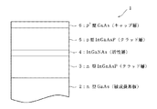
図1は、本発明の半導体発光素子及び半導体発光素子の製造方法の第1の実施の形態を適用した半導体発光素子1の正面断面図である。
【0045】
図1において、半導体発光素子1は、n型GaAs層で形成された被成長基板2上にクラッド層3、活性層4、クラッド層5及びキャップ層6が順次積層されており、V族にNを含んでN系混晶半導体材料であるInGaNAs層をGaAs基板2上に形成したものである。
【0046】
クラッド層3は、GaAsである被成長基板2に格子整合しバンドギャップエネルギーが1.53eVであるInGaAsPを用いた構造(n型InGaAsP層)となっており、Alを含まない材料である。
【0047】
発光層である活性層4は、クラッド層3上に形成され、InGaNAs層、すなわち、Nを含む混晶半導体であるGaaIn1-aNbAs1-b(0<b<1)層で形成されている。
【0048】
クラッド層5は、活性層4上に形成され、InGaAsPを用いた構造(p型InGaAsP層)となっている。キャップ層6は、p+ 型GaAs層で形成されている。
【0049】
次に、この半導体発光素子1の製造方法について、図2に基づいて説明する。図2は、MOCVD(Metal Organic Chemical Vapor Deposition )装置10の反応室部分の概略構成図であり、MOCVD装置10は、横型炉である。なお、MOCVD装置10としては、横型炉に限るものではなく、縦型炉であってもよい。
【0050】
MOCVD装置10は、内部に反応室11を有する石英反応管12の周囲に冷却管13が配設されており、石英反応管12には、反応室11に原料ガスとキャリアガスを供給するためのガス供給口14が形成されている。また、石英反応管12には、図示しない排気装置に接続されて、反応室11内のガスを排気する排気管15が接続されている。石英反応管12の反応室11内には、カーボンサセプター16が配設されており、カーボンサセプター16は、高周波加熱コイル17により加熱される。高周波加熱コイル17により加熱されるカーボンサセプター16の温度は、熱電対18により検出される。カーボンサセプター16上には、上記被成長基板2がセットされる。
【0051】
このMOCVD装置10を使用して半導体発光素子1を製造するには、カーボンサセプター16に被成長基板2としてGaAs基板をセットし、図示しない排気装置により反応室11内の圧力を1.3×10⁴ Paに減圧する。そして、熱電対18により温度検出を行いつつ、高周波加熱コイル17によりカーボンサセプター16を加熱して、被成長基板2であるGaAs基板を所定温度に加熱制御し、原料ガスとキャリアガスを同時にガス供給口14から反応室11内に供給することにより、被成長基板2であるGaAs基板上に順次クラッド層3、活性層4、クラッド層5及びキャップ層6を積層する。
【0052】
まず、上記MOCVD装置10を用いて被成長基板2であるGaAs層上にInGaNAs層を形成する場合について説明する。
【0053】
原料ガスとしては、III 族原料として、TMG(トリメチルガリウム)、TEG(トリエチルガリウム)、TMI(トリメチルインジウム)、あるいは、TEI(トリエチルインジウム)を、Asの原料として、AsH3 (アルシン)を、Nの原料として、有機系窒素化合物であるDMHy(ヂメチルヒドラジン)、MMHy(モノメチルヒドラジン)、あるいは、TBA(ターシャリブチルアミン)等を使用し、キャリアガスとしては、H2 を使用する。
【0054】
上記条件で原料ガスとキャリアガスを同時にガス供給口14から反応室11内に供給すると、原料ガスの熱分解とGaAs層である被成長基板2の表面反応により、結晶成長し、成膜される。
【0055】
そして、原料材料としてのTMG:4.0×10⁻⁶mol/min〜4.0×10-5mol/min、TMI:4.4×10-7mol/min〜4.4×10-6mol/min、AsH3 :6.0×10⁻⁵mol/min(0.4sccm)〜2.2×10-3mol/min(46.4sccm)、DMHy:5.0×10-4mol/minに、キャリアガスであるH2 を加えて、トータルで6l/minを供給し、AsH3 の分圧を、0.9〜102Pa、成長温度を、450℃〜700℃とする。
【0056】
具体的には、例えば、TMG:2.0×10⁻⁵mol/min、TMI:2.2×10-6mol/min、AsH3 :3.3×10⁻⁴mol/min(7sccm)、DMHy:6.4×10-3mol/minを原材料ガスとして使用し、AsH3 分圧が、15.4Paで、成長温度を、630℃としたとき、成長速度、1.7μm/hで、GaAs層である被成長基板2上に、In0.11Ga0.89N0.04As0.96層が形成された。
【0057】
この作製したIn0.11Ga0.89N0.04As0.96層を用いて積層構造として形成した半導体発光素子1は、GaAsである被成長基板2に格子整合しており、Arレーザー(448nm)を励起光源、Ge−フォトダイオードを受光器として、この半導体発光素子1について、室温でPL(フォトルミネッセンス)測定を行ったところ、中心波長は、約1.3μmであった。この波長帯は、光通信分野に応用することができる。
【0058】
また、TMIを減らし、AsH3 を増やして成長したところ、In0.06Ga0.94N0.02As0.98層が形成された。この層もGaAs基板に格子整合しており、PL中心波長は、約1.17μmであった。このようなInGaNAs層の発光波長は、In及びNの組成を大きくすることで長波長化することができる。
【0059】
すなわち、一般に、GaAsにInを添加すると、格子定数が、大きくなり、バンドギャップエネルギーが、小さくなる効果がある。これに対して、GaAsにNを添加すると、格子定数が、小さくなり、バンドギャップエネルギーが、同様に小さくなる効果がある。すなわち、InxGa1-xAsにNを添加すると、バンドギャップエネルギーが、InxGa1-xAsより小さくなり、さらに格子定数がGaAsと一致する条件が存在する。このようにInGaNAs層は、GaAs基板に格子整合可能であるので、GaAsのバンドギャップエネルギーに対応する約870nm(室温)の発光波長より長波長の発光素子を、従来からあるGaAsに格子整合せずGaAsよりも格子定数が大きいInGaAsを発光層に用いた場合に比べて、容易に、かつ、高品質に形成でき、しかも、1.3μm帯、1.5μm帯のより長波長の素子を形成することも可能となる。
【0060】
そこで、上記MOCVD装置10を使用して、GaAs層である被成長基板2に格子整合しているIn0.06Ga0.94N0.02As0.98層を用いて、上記図1に示した積層構造の半導体発光素子1を形成した。この場合、上述のように、クラッド層3、5には、GaAs層である被成長基板2に格子整合しバンドキャップエネルギーが、1.35eVであるInGaAsP層を用いており、Alを含まない材料で形成されている。
【0061】
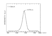
上記半導体発光素子1のウエハを用いて、ストライプ幅が5μmで、素子長が200μmの絶縁膜ストライプ構造のデバイスを作製し、LED(Light Emitting Diode)動作をテストしたところ、適切なLED動作を得た。このときの発光スペクトルは、動作電流が、50mAで、図3に示すように、中心波長が1176nmであり、PLスペクトルを反映したスペクトルとなっている。
【0062】
このように、本実施の形態の半導体発光素子1は、発光層4であるInGaNAs活性層と接するクラッド層3、5が、Alを含んでいない、すなわち、活性領域(発光層4と発光層4に接するクラッド層3、5)に活性なAlが含まれていないので、Nを含む混晶半導体に適した低い成長温度においても、Alを含んだ層の成長表面に形成されやすかった製造装置内及び原料ボンベ内のO(酸素)がGaAs層である被成長基板2の表面に取り込まれて発生する劣化の起源となる非発光再結合センターを低減させることができる。したがって、発光効率が高く、寿命の長いN系V族混晶半導体発光素子1を容易に製造することができる。
【0063】
なお、上記実施の形態においては、InGaNAs活性層である発光層4が、被成長基板2としてのGaAs層に格子整合している場合について説明したが、InGaNAs活性層4は、GaAs層である被成長基板2に完全に格子整合していなくてもよく、歪を持っていても臨界膜厚以内の厚さであればよい。
【0064】
また、本実施の形態においては、N系V族混晶半導体としてInGaNAsを使用した場合について説明したが、N系V族混晶半導体としては、上記のものに限るものではなく、例えば、Pを含んだInGaNAsP等の他の混晶半導体についても同様に適用することができる。
【0065】
さらに、クラッド層3、5としては、活性層である発光層4よりもバンドギャップエネルギーの大きいGadIn1-dNeAsfP1-e-f 層(0≦d≦1、0≦e<1、0≦f≦1)を用いることができ、この場合にも、同様の効果を得ることができる。
【0066】
また、光通信に用いられる1.3μm帯(1.25〜1.35μm)の波長の半導体発光素子1は、GaAsである被成長基板2に格子整合する材料では、発光層4の組成を、ほぼIn0.11Ga0.89N0.04As0.96とすることで得ることができる。
【0067】
図4は、本発明の半導体発光素子及び半導体発光素子の製造方法の第2の実施の形態を示す図であり、本実施の形態は、GaAs基板に格子整合しているIn0.14Ga0.86N0.05As0.95活性層(井戸層)を用いて積層構造を形成したものである。
【0068】
図4は、半導体発光素子20の積層構造を示した正面断面図であり、半導体発光素子20は、n型GaAs層である被成長基板21上に、n型InGaAsP層で形成されたクラッド層22、InGaAsP層で形成されたガイド層23、InGaNAs層で形成された井戸層24、InGaAsP層で形成されたガイド層25、p型InGaAsP層で形成されたクラッド層26及びp+ 型GaAs層で形成されたキャップ層27が順次積層されている。
【0069】
発光層である井戸層24は、GaAs層である被成長基板21に格子整合しているIn0.14Ga0.86N0.05As0.95層で形成されている。
【0070】
半導体発光素子20は、ガイド層(光導波層)23、25には、GaAs層である被成長基板21に格子整合しバンドギャップエネルギーが1.53eVであるInGaAsPを用い、クラッド層22、26には、GaAs層である被成長基板21に格子整合しバンドギャップエネルギーが1.85eVであるInGaAsPを用いたSCH−SQW構造(Separate Confinement Hetero-Structure-Single Quantum Well 構造)となっている。
【0071】
本実施の形態の半導体発光素子20は、上述のように、発光層である井戸層(活性層)24と接する層(ガイド層23、25)が、Alを含んでいない、すなわち、活性領域である発光層24とガイド層23、25に活性なAlを含んでいないので、Nを含む混晶半導体に適した低い成長温度においても、Alを含んだ層の成長表面に形成されやすかった製造装置内及び原料ボンベ内のO(酸素)が基板表面に取り込まれて発生する劣化の起源となるような非発光再結合センターを、低減させることができ、半導体発光素子20を、発光効率が高く、寿命の長いものとすることができる。
【0072】
この半導体発光素子20の発光波長を測定したところ、発光波長は、約1.3μmであった。この場合、井戸層24のIn組成を11%よりも大きくすることで、バルクの発光波長は、1.3μmより長波長となるが、井戸層(発光層)24の膜厚を、例えば、20nm以下とし、量子効果を利用することで、波長を、1.3μmに制御することができる。
【0073】
なお、本実施の形態においては、InGaNAs層である井戸層(活性層)24を、In0.14Ga0.86N0.05As0.95層としているが、InGaNAs層である活性層24としては、他の組成であってもよい。
【0074】
また、井戸層(活性層)24は、GaAs層である被成長基板21に格子整合しているが、完全に格子整合していなくともよく、歪を持っていても臨界膜厚以内の厚さであればよい。
【0075】
さらに、本実施の形態においては、N系V族混晶半導体として、InGaNAsを用いた場合について説明しているが、N系V族混晶半導体としては、Pを含んだInGaNAsP等他の混晶半導体であっても、同様に適用することができる。
【0076】
また、ガイド層23、25としては、GaAs層である被成長基板21に格子整合可能な組成、あるいは、格子整合しておらず歪を持っていても臨界膜厚以内の厚さのGadIn1-dNeAsfP1-e-f層 (0≦d≦1、0≦e<1、0≦f≦1)であっても、同様に適用することができる。
【0077】
さらに、半導体発光素子20は、クラッド層22、26にAlを含んでいないので、ガイド層23、25には、Nを含んでいてもよい。この場合、ガイド層23、25は、クラッド層22、26よりもバンドギャップエネルギーの小さい材料である必要がある。
【0078】
また、本実施の形態では、SQW構造としているが、井戸層を複数層用いた多重量子井戸構造を用いてもよい。この場合、ガイド層には、クラッド層よりバンドギャップエネルギーの小さいGadIn1-dNeAsfP1-e-f 層(0≦d≦1、0≦e<1、0≦f≦1)を用いることができる。
【0079】
図5は、本発明の半導体発光素子及び半導体発光素子の製造方法の第3の実施の形態を示す図であり、本実施の形態は、GaAs基板に格子整合しているIn0.14Ga0.86N0.05As0.95活性層を用いて積層構造を形成したものである。
【0080】
図5は、半導体発光素子30の積層構造を示した正面断面図であり、半導体発光素子30は、n型GaAs層である被成長基板31上に、n型AlGaAs層で形成されたクラッド層32、InGaAsP層で形成されたガイド層33、InGaNAs層で形成された井戸層(発光層)34、InGaAsP層で形成されたガイド層35、p型AlGaAs層で形成されたクラッド層36及びp+ 型GaAs層で形成されたキャップ層37が順次積層されている。そして、井戸層34は、GaAsである被成長基板31に格子整合しているIn0.14Ga0.86N0.05As0.95層により形成されている。
【0081】
すなわち、半導体発光素子30は、GaAs層である被成長基板31に格子整合しバンドギャップエネルギーが1.53eVのInGaAsP層をガイド層33、35とし、Al組成0.8のAlGaAs層をクラッド層32、36としたSCH−SQW構造となっている。
【0082】
上記半導体発光素子30は、発光層であるInGaNAs層で形成された井戸層34にAlGaAs層で形成されたクラッド層32、36が直接接していない、すなわち、活性領域(発光層34とガイド層33、35)が活性なAlを含んでいないので、Nを含む混晶半導体に適した低い成長温度においても、Alを含んだ層の成長表面に形成されやすかった製造装置及び原料ボンベ内のO(酸素)が基板表面に取り込まれて発生する劣化の起源となるような非発光再結合センターを、低減させることができる。したがって、発光効率が高く、寿命の長いGaAs基板格子整合系長波長半導体レーザーを形成することができる。
【0083】
この半導体発光素子30の発光波長を測定したところ、発光波長は、約1.3μmであった。
【0084】
本実施の形態においては、半導体発光素子30は、AlGaAs層をクラッド層32、36に用いている。ここで、例えば、InGaPをクラッド層に用いた場合と比較すると、AlGaAsの熱抵抗率は、InGaPの熱抵抗率の約1/2倍である。クラッド層の厚さは、一般的に、1.5μm程度は必要であり、熱抵抗率の小さい材料の方が電流注入時の活性領域の温度上昇が小さいので、効率の低下等の問題を抑えられるので好ましい。このような観点から本実施の形態の素子においては、AlGaAsをクラッド層32、36に用いた。
【0085】
このように膜厚の薄いInGaAsPであるガイド層33、35の外側に熱抵抗率が低く屈折率が低くバンドギャップエネルギーが大きいAlGaAs層をクラッド層32、36に用いているので、キャリアと光の閉じ込め効率がさらに向上して、しきい電流密度が下がり、発光効率も高くなった。このように素子寿命が長く、しきい電流密度が低く、発光効率が高いGaAs基板格子整合系長波長半導体レーザーである半導体発光素子30を形成できた。
【0086】
なお、InGaNAs層である井戸層(活性層)34は、他の組成でもよく、また、GaAs層である被成長基板31に完全に格子整合していなくともよく、歪を持っていても臨界膜厚以内の厚さならかまわない。また、本実施の形態においては、N系V族混晶半導体としてInGaNAsの場合について説明したが、Pを含んだInGaNAsP等の他の混晶半導体についても適用できる。
【0087】
さらに、ガイド層33、35は、GaAs層である被成長基板31に格子整合可能な組成、もしくは、格子整合していなくても歪を持っていても臨界膜厚以内の厚さであるInxGa1-xAsyP1-y(0≦x<1、0≦y≦1)であればかまわない。また、AlGaAs層であるクラッド層32、35のAl組成は、ガイド層33、35よりも伝導帯のエネルギーが大きければ、他の組成であってもよい。
【0088】
図6は、本発明の半導体発光素子及び半導体発光素子の製造方法の第4の実施の形態を示す図であり、本実施の形態は、クラッド層として、GaAs層である被成長基板に格子整合しているInGaAlP層を用いたものである。
【0089】
図6において、半導体発光素子40は、n型GaAsで形成された被成長基板41上に、n型InGaAlP層で形成されたクラッド層42、InGaAsP層で形成されたガイド層43、InGaNAs層で形成された井戸層44、InGaAsP層で形成されたガイド層45、p型InGaAlP層で形成されたクラッド層46及びp+ 型GaAs(キャップ層)47が順次積層されている。
【0090】
半導体発光素子40は、クラッド層42、46が、GaAs層で形成された被成長基板41に格子整合しているInGaAlP層により形成されている。InGaAlP系は、AlGaAs系よりも大きなバンドギャップエネルギーとなる組成が存在しており、キャリア及び光閉じ込め効率を高くすることができる。さらに、AlGaAs系は、GaAs層である被成長基板41に対して、格子定数がわずかにずれるが、InGaAlP系は、完全に格子整合させることができるというメリットがある。
【0091】
したがって、発光効率が高く、寿命の長いGaAs基板格子整合系長波長半導体レーザーである半導体発光素子40を形成することができる。
【0092】
図7は、本発明の半導体発光素子及び半導体発光素子の製造方法の第5の実施の形態を示す図であり、本実施の形態は、InGaNAs活性層がGaAs基板に完全には格子整合せず臨界膜厚以内の厚さで歪を有しているものである。
【0093】
図7において、半導体発光素子50は、n型GaAsで形成された被成長基板51上に、n型AlGaAs層で形成されたクラッド層52、InGaAsP層で形成されたガイド層53、InGaNAs層で形成された井戸層(圧縮層)54、InGaAsP層で形成されたガイド層55、p型AlGaAs層で形成されたクラッド層56及びp+ 型GaAsで形成されたキャップ層57が順次積層されている。
【0094】
半導体発光素子50は、そのInGaNAs層で形成された井戸層54が、第3の実施の形態の半導体発光素子30のInGaNAs層で形成された井戸層34に比較して、In組成が大きく、格子定数がGaAs層である被成長基板51よりも大きく、圧縮歪を有している。また、この半導体発光素子50の発光波長を測定したところ、発光波長は、約1.3μmであった。第3の実施の形態のように格子整合する材料で量子効果を利用するためには、波長1.3μmの場合、In組成を11%より大きく、N組成を、4%より大きくすることにより、可能である。
【0095】
ところが、Nは、成長中の基板表面から離脱しやすく、N組成の大きいN系V族混晶半導体を得ることが難しい。また、本出願の発明者の実験によると、N組成が大きくなると、PL(フォトルミネッセンス)強度が弱くなり、結晶性の悪化が確認された。したがって、波長が長くなるほど作製しにくいのが現状である。
【0096】
ところが、同じN組成のInGaNAsでは、Inの組成が大きい方が格子定数が大きくなり、発光波長が、長波長になる。そこで、この性質を利用すると、例えば、波長1.3μmでGaAs層で形成された被成長基板51に格子整合させるためには、In0.11Ga0.89N0.04As0.96である必要があるが、In組成を11%より大きくすると、N組成が4%より小さい条件で、波長1.3μmを得ることができるようになる。この場合、格子定数は、GaAs層である被成長基板51よりも大きくなる。このように格子定数をGaAs層である被成長基板51よりも大きくすると、格子整合条件に比べて小さいN組成で目的の波長を得ることができるので、作製を容易にすることができ、さらに、発光効率を高くすることができる。
【0097】
そこで、本実施の形態の半導体発光素子50では、Inの組成を11%よりも大きくし、InGaNAs層である井戸層(活性層)54の格子定数をGaAs層である被成長基板51より大きくしているので、小さいN組成で形成することができ、半導体発光素子50の作製を容易なものとすることができるとともに、発光効率を高くすることができる。また、本実施の形態の半導体発光素子50は、歪量子井戸の効果による閾電流密度が低下する効果もある。このため、光ファイバー通信用光源として有効である。もちろんInGaNAs層は、他の波長に設定することもできる。
【0098】
図8は、本発明の半導体発光素子及び半導体発光素子の製造方法の第6の実施の形態を適用した半導体発光素子を示す図であり、本実施の形態は、InGaNAs活性層がGaAs基板に完全には格子整合せずに臨界膜厚以内の厚さで歪を持っているものである。
【0099】
図8は、本実施の形態の半導体発光素子60の正面断面図であり、図8において、半導体発光素子60は、n型GaAs層で形成された被成長基板61、n型AlGaAs層で形成されたクラッド層62、InGaAsP層で形成されたガイド層63、歪補償型MQW(多重量子井戸)構造層64、InGaAsPで形成されたガイド層65、p型AlGaAs層で形成されたクラッド層66及びp+ 型GaAs層で形成されたキャップ層67が順次積層されている。
【0100】
半導体発光素子60は、上記第5の実施の形態と以下の点で異なる。すなわち、半導体発光素子60は、その活性領域が歪補償型MQW(多重量子井戸)構造層64で形成されており、MQW構造層64のInGaNAs井戸層の格子定数が、GaAsで形成された被成長基板61よりも大きな圧縮歪を有し、さらに、MQW構造層64のInGaAsPバリア層の格子定数が、GaAsで形成された被成長基板61よりも小さな引っ張り歪を有している。
【0101】
上記MQW構造層64のInGaNAsP系井戸層とInGaAsP系バリア層は、ともに組成を変えることで、同じバンドギャップエネルギーを有した条件で格子定数をGaAsの被成長基板61よりも大きくしたり、小さくしたり変えることが可能な材料系である。これは、AlGaAs系バリア層ではできない。すなわち、AlGaAs系バリア層を用いた場合に比べて、InGaAsP系バリア層を用いることで、InGaNAsP系井戸層の歪を補償することが可能となり、適正な歪量を持つ組成に制御することで、井戸層の組成の自由度を大きくしたり、井戸層の数を多くすることができる。
【0102】
なお、本実施の形態では、MQW構造64のInGaNAs井戸層を圧縮層、InGaAsPバリア層を引っ張り歪層としているが、InGaNAs井戸層を引っ張り歪層、InGaAsPバリア層を圧縮歪層としても、同様に適正な歪量を持つ組成に制御することで、歪量子井戸の効果を得ることができる。
【0103】
図9は、本発明の半導体発光素子及び半導体発光素子の製造方法の第7の実施の形態を示す図であり、本実施の形態は、GaInNAs層を井戸層とし、GaInNAsPをバリア層とした歪補償型MQW(多重量子井戸)構造を用いたものに適用したものである。
【0104】
図9は、本実施の形態の半導体発光素子70の正面断面図であり、図9において、半導体発光素子70は、n型GaAs層で形成された被成長基板71、n型AlGaAs層で形成されたクラッド層72、InGaAsP層で形成されたガイド層73、歪補償型MQW(多重量子井戸)構造層74、InGaAsPで形成されたガイド層75、p型AlGaAs層で形成されたクラッド層76及びp+ 型GaAs層で形成されたキャップ層77が順次積層されている。
【0105】
半導体発光素子70は、その歪補償型MQW(多重量子井戸)構造層74のInGaNAs井戸層の格子定数が、GaAs層である被成長基板71よりも大きな圧縮歪を有しており、さらに、MQW構造層74のInGaNAsPバリア層の格子定数が、GaAs層である被成長基板71よりも小さな引っ張り歪を有している。また、半導体発光素子70は、クラッド層72、76に、AlGaAs層を用いており、Alを含んだ層とNを含んだ層が直接接しない構造となっている。
【0106】
したがって、本実施の形態の半導体発光素子70においても、歪補償型MQW(多重量子井戸)構造を用いた効果を得ることができる。
【0107】
本実施の形態においては、InGaNAsPバリア層の成長条件は、MQW構造層74のInGaNAs井戸層の成長条件に対してPの原料(本実施の形態では、PH3 )を添加したものであり、In、Ga、N、Asの原料の供給量は変えていない。
【0108】
一般に、InGaNAsに対してPを添加すると、バンドギャップエネルギーは大きくなり、格子定数は小さくなる効果がある。そして、本実施の形態の半導体発光素子70のMQW構造層74のInGaNAs井戸層の格子定数が、GaAs層である被成長基板71より大きい場合、Pの添加量を制御することによって格子定数をGaAs層である被成長基板71に格子整合させたり、GaAs層である被成長基板71より小さくしたりすることができる。
【0109】
また、本実施の形態の半導体発光素子70のMQW構造層74は、井戸層とバリア層の両方にNを含んでいるので、他のV族原料に比べ、一般に供給量の多いNの原料を井戸層とバリア層の成長時に、オン/オフ(被成長基板71に供給する、しない)する必要がなくなるので、界面の制御を容易に行うことができる。
【0110】
なお、本実施の形態では、In、Ga、N、Asの原料の供給量を、変えないで作製したが、変えても、同様に適用することができる。
【0111】
また、本実施の形態においては、MQW構造層74の井戸層にPを含んでいない場合について説明したが、井戸層にPを含んでいてもバリア層のP組成をさらに大きくする等の方法により、バリア層のバンドギャップエネルギーの方を大きくすることにより、適用することができる。
【0112】
図10は、本発明の半導体発光素子及び半導体発光素子の製造方法の第8の実施の形態を示す図であり、本実施の形態は、0.8μm帯等の固体レーザ励起用などの高出力半導体レーザに適用したものである。
【0113】
図10は、本実施の形態の半導体発光素子80の正面断面図であり、図10において、半導体発光素子80は、n型GaAs層で形成された被成長基板81、n型InGaP層で形成されたクラッド層82、InGaAsP層で形成されたガイド層83、InGaNAsP層で形成された井戸層(活性層)84、InGaAsP層で形成されたガイド層85、p型InGaP層で形成されたクラッド層86及びp+ 型GaAs層で形成されたキャップ層87が順次積層されている。
【0114】
すなわち、半導体発光素子80は、その活性層(井戸層)84として、バンドギャップエネルギーが、1.54eVであるInGaNAsP層を、ガイド層(光導波層)83、85として、GaAs層である被成長基板81に格子整合しバンドギャップエネルギーが1.83eVであるInGaAsP層を、そして、クラッド層82、86として、GaAs層である被成長基板81に格子整合しバンドギャップエネルギーが1.91eVであるInGaPを用いたSCH−SQW構造となっている。そして、この半導体発光素子80の発振波長は、約0.81μmである。
【0115】
従来、0.8μm帯等の固体レーザ励起用等の高出力半導体レーザにおいては、活性層に接するクラッド層やガイド層には、AlGaAsが多く用いられているが、光学損傷が生じやすく、信頼性に問題があった。そこで、従来、InGaAsP系材料によりAlフリーの材料系が試作されているが、InGaAsP系材料は、AlGaAs系材料に比べて、伝導帯のバンドオフセットが小さいため、活性層からのキャリアリークが大きくなり、信頼性は良好であるが、高出力半導体レーザとしては、他の素子特性が十分ではなかった。
【0116】
このような従来の高出力半導体レーザに対して、本実施の形態の半導体発光素子80は、活性層(井戸層)84がInGaNAsPで形成され、Nが添加されたものとなっている。このように、Nを添加すると、バンドギャップを小さくすることができるとともに、伝導帯及び価電子帯のエネルギーを小さくすることができる。したがって、InGaAs系材料をクラッド層82、86やガイド層83、85に用いても、伝導帯のバンドオフセットが大きくなり、活性層84からのキャリアリークが小さくなる。その結果、閾値電流密度が低くなり、高温特性等を良好なものとすることができる。
【0117】
また、半導体発光素子80は、発光層84であるInGaNAsP層と接する層には、Alを含んでいない、すなわち、活性領域(発光層84とガイド層83、85)に活性なAlを含んでいないので、Nを含む混晶半導体に適した低い成長温度においても、Alを含んだ層の成長表面に形成されやすかった製造装置内及び原料ボンベ内のO(酸素)が基板表面に取り込まれて発生する劣化の起源となるような非発光再結合センターを低減させることができる。したがって、信頼性が高く、かつ、他の素子特性も良好な高出力半導体レーザである高出力な半導体発光素子80を容易に製造することができる。
【0118】
なお、本実施の形態においては、活性層84としてInGaNAsP層を用いているが、他の組成であってもよい。
【0119】
また、InGaNAsP層である活性層84が、被成長基板81としてのGaAs層に完全に格子接合している場合について説明したが、GaAs層である被成長基板81に完全には格子整合していなくてもよく、歪みを持っていても、臨界膜厚以内の厚さであればよい。
【0120】
さらに、ガイド層83、85としては、GaAs層である被成長基板81に格子整合可能な組成、あるいは、格子整合せずに、歪みを持っていても、臨界膜厚以内の厚さ、すなわち、GadIn1-dNeAsfP1-e-f層 (0≦d≦1、0≦e<1、0≦f≦1)であっても、同様に適用することができる。
【0121】
また、半導体発光素子80は、クラッド層82、86にAlを含んでいないので、ガイド層83、85には、Nを含んでいてもよい。この場合、ガイド層83、85は、クラッド層82、86よりもバンドギャップエネルギーの小さい材料である必要がある。
【0122】
さらに、本実施の形態では、SQW構造としているが、井戸層を複数層用いた多重量子井戸構造を用いてもよい。この場合、バリア層には、クラッド層よりバンドギャップエネルギーの小さいGadIn1-dNeAsfP1-e-f 層(0≦d≦1、0≦e<1、0≦f≦1)を用いることができる。
【0123】
以上、本発明者によってなされた発明を好適な実施の形態に基づき具体的に説明したが、本発明は上記のものに限定されるものではなく、その要旨を逸脱しない範囲で種々変更可能であることはいうまでもない。
【0124】
【発明の効果】
請求項1記載の発明の半導体発光素子によれば、V族にNを含んだN系混晶半導体材料を活性層としGaAs基板上に形成される半導体発光素子において、発光層を、Nを含む混晶半導体Ga a In 1-a N b As c P 1-b-c (0≦a≦1、0<b<1、0≦c<1)層で形成し、発光層と直接接するクラッド層、ガイド層あるいはバリア層を、発光層よりもバンドギャップエネルギーの大きいNとPを含むGa d In 1−d N e P f As 1−e−f (0≦d≦1、0<e<1、0<f<1)層で形成しているので、GaAs基板上にAlを含まない系でヘテロ構造を作製することができ、半導体発光素子を発光効率が高く、寿命の長いものとすることができる。
【0126】
請求項2記載の発明の半導体発光素子によれば、発光層を、GaaIn1-aNbAscP1-b-c(0≦a≦1、0<b<1、0≦c<1)層で形成し、バリア層及びガイド層を、NとPを含むGa d In 1−d N e P f As 1−e−f (0≦d≦1、0<e<1、0<f<1)層で形成し、クラッド層を、バリア層及びガイド層よりもバンドギャップエネルギーの大きいGavIn1-vAswP1-w(0<v≦1、0≦w≦1)層で形成しているので、Alを含まない系で多重量子井戸を用いた素子を形成することができ、GaInNAsP層と接する層をAlを含まない層、すなわち、活性領域(発光層と発光層に接する層)に活性なAlを含まない層で形成することができる。したがって、半導体発光素子を発光効率が高く、寿命の長いものとすることができる。
【0127】
請求項3記載の発明の半導体発光素子によれば、発光層を、GaaIn1-aNbAscP1-b-c(0≦a≦1、0<b<1、0≦c<1)層で形成し、バリア層を、NとPを含むGa d In 1−d N e P f As 1−e−f (0≦d≦1、0<e<1、0<f<1)層で形成し、ガイド層を、発光層よりもバンドギャップエネルギーの大きいGaxIn1-xAsyP1-y(0<x≦1、0≦y≦1)層で形成し、クラッド層を、バリア層及びガイド層よりもバンドギャップエネルギーの大きいAluGa1-uAs(0<u≦1)層で形成しているので、GaInNAsP層と接する層を、Alを含まない層、すなわち、活性領域(発光層と発光層に接する層)に活性なAlを含んでいない層とすることができ、発光効率が高く、寿命の長い半導体発光素子を提供することができるとともに、キャリアと光の閉じ込め効率が良好で、閾電流密度が低く、発光効率の高い半導体発光素子を提供することができ、かつ、熱抵抗率の小さいAlGaAsをクラッド層に用いているので、素子動作時の活性領域の温度上昇を抑制することができ、発光効率の低下等の特性の悪化をさらに低減させることができる。
【0128】
請求項2記載の発明の半導体発光素子によれば、発光層とバリア層とガイド層とクラッド層が積層された積層構造からなり、GaAs基板上に形成される半導体発光素子において、発光層を、GaaIn1-aNbAscP1-b-c(0≦a≦1、0<b<1、0≦c<1)層で形成し、バリア層を、NとPを含むGadIn1−dNePfAs1−e−f(0≦d≦1、0<e<1、0<f<1)層で形成し、ガイド層を、発光層よりもバンドギャップエネルギーの大きいGaxIn1-xAsyP1-y(0<x≦1、0≦y≦1)層で形成し、クラッド層を、バリア層及びガイド層よりもバンドギャップエネルギーの大きいInsGatAl1-s-tP(0<s<1、0≦t<1、0<1−s−t)層で形成しているので、GaInNAsP層と接する層を、Alを含まない層、すなわち、活性領域(発光層と発光層に接する層)に活性なAlを含んでいない層とすることができ、半導体発光素子を発光効率が高く、寿命の長いものとすることができるとともに、キャリアと光の閉じ込め効率が良好で、閾電流密度が低く、発光効率の高い半導体発光素子を提供することができ、かつ、AlGaAs系は、わずかにGaAs基板に対し格子定数がずれるが、InGaAlP系を用いると、完全に格子整合させることができる。
【0129】
請求項5記載の発明の半導体発光素子によれば、発光層が、ミスフィット転位の発生する臨界歪量以内の格子歪を有しているので、N組成を小さくすることができ、作製が容易で、かつ、N組成の増加に伴う結晶性の低下を抑制することができる。したがって、発光効率をより一層向上させることができる。
【0130】
請求項6記載の発明の半導体発光素子によれば、発光層が、ミスフィット転位の発生する臨界歪量以内の圧縮格子歪を有し、バリア層が、ミスフィット転位の発生する臨界歪量以内の引っ張り格子歪を有しているので、AlGaAsをバリア層とした場合にはできなかった歪補償型の量子井戸素子とすることができ、井戸層(発光層)の歪を補償して、適正な歪量を持つ組成に制御し、井戸層の組成の自由度を大きくしたり、井戸層の数を多くすることができる。したがって、半導体発光素子を、製造が容易で、発光効率が高く、かつ、寿命の長いものとすることができる。
【0131】
請求項7記載の発明の半導体発光素子によれば、発光層が、ミスフィット転位の発生する臨界歪量以内の引っ張り格子歪を有し、バリア層が、ミスフィット転位の発生する臨界歪量以内の圧縮格子歪を有しているので、AlGaAsをバリア層とした場合にはできなかった歪補償型の量子井戸素子とすることができ、井戸層(発光層)の歪を補償して、適正な歪量を持つ組成に制御し、井戸層の組成の自由度を大きくしたり、井戸層の数を多くすることができる。したがって、半導体発光素子を、製造が容易で、発光効率が高く、かつ、寿命の長いものとすることができる。
【0132】
請求項8記載の発明の半導体発光素子によれば、発光層を、Nを含む混晶半導体であるGaaIn1-aNbAs1-b(0<b<1)層で形成し、該発光層のIn組成(1−a)が、11%より大きく、格子定数が、GaAs基板より大きく、発光波長が、1.3μm帯であるものとしているので、格子整合系に比較してN組成を小さくしても一定波長を形成でき、半導体発光素子を、再生が容易であるとともに、N組成増加に伴う結晶性の低下を抑制して、発光効率が良好で、光ファイバー通信用光源に適用することができるものとすることができる。
【0133】
請求項9記載の発明の半導体発光素子の製造方法によれば、クラッド層、ガイド層あるいはバリア層を、P原料供給の有無あるいはP原料の供給量の増減によって、そのP組成が発光層のP組成よりも大きい層に形成しているので、他のV族原料に比べて一般に供給量の多いNの原料を発光層とバリア層の成長時に供給したり、供給を止めたりする必要がなくなり、例えば、気相成長のような場合には、ガスの流れの乱れを抑えることができ、界面の制御を容易に行なうことができる。したがって、発光効率が高く、寿命の長い半導体発光素子を容易に製造することができる。
また、請求項10記載の発明によれば、請求項1乃至請求項9のいずれか一項に記載の半導体発光素子の製造方法であって、Nを含む半導体層は、Nの原料として有機系窒素化合物を用いた減圧MOCVD法(有機金属気相成長法)により結晶成長されるので、発光効率が高く、寿命の長い半導体発光素子を容易に製造することができる。
また、請求項11記載の発明によれば、請求項1乃至請求項9のいずれか一項に記載の半導体発光素子を用いた光ファイバー通信システムであるので、信頼性の高い光ファイバー通信システムを提供することができる。
【図面の簡単な説明】
【図1】本発明の半導体発光素子及び半導体発光素子の製造方法の第1の実施の形態を適用した半導体発光素子の成長層の正面断面図。
【図2】図1の半導体発光素子を製造するためのMOCVD装置の反応室部分の概略構成図。
【図3】図1の半導体発光素子の発光スペクトルを示す図。
【図4】本発明の半導体発光素子及び半導体発光素子の製造方法の第2の実施の形態を適用した半導体発光素子の成長層の正面断面図。
【図5】本発明の半導体発光素子及び半導体発光素子の製造方法の第3の実施の形態を適用した半導体発光素子の成長層の正面断面図。
【図6】本発明の半導体発光素子及び半導体発光素子の製造方法の第4の実施の形態を適用した半導体発光素子の成長層の正面断面図。
【図7】本発明の半導体発光素子及び半導体発光素子の製造方法の第5の実施の形態を適用した半導体発光素子の成長層の正面断面図。
【図8】本発明の半導体発光素子及び半導体発光素子の製造方法の第6の実施の形態を適用した半導体発光素子の成長層の正面断面図。
【図9】本発明の半導体発光素子及び半導体発光素子の製造方法の第7の実施の形態を適用した半導体発光素子の成長層の正面断面図。
【図10】本発明の半導体発光素子及び半導体発光素子の製造方法の第8の実施の形態を適用した半導体発光素子の成長層の正面断面図。
【符号の説明】
1 半導体発光素子
2 被成長基板
3 クラッド層
4 活性層
5 クラッド層
6 キャップ層
10 MOCVD装置
11 反応室
12 石英反応管
13 冷却管
14 ガス供給口
15 排気管
16 カーボンサセプター
17 高周波加熱コイル
18 熱電対
20、30、40、50、60、70、80 半導体発光素子
21、31、41、51、61、71、81 被成長基板
22、32、42、52、62、72、80 クラッド層
23、33、43、53、63、73、83 ガイド層
24、34、44、54、84 井戸層
25、35、45、55、65、75、85 ガイド層
26、36、46、56、66、76、86 クラッド層
27、37、47、57、67、77、87 キャップ層
64、74 歪補償型MQW構造層[0001]
BACKGROUND OF THE INVENTION
The present invention relates to a semiconductor light emitting device, a method for manufacturing the semiconductor light emitting device, and an optical fiber communication system, and more particularly to a semiconductor light emitting device used for a semiconductor laser, a light emitting diode, and the like, a manufacturing method therefor, and an optical fiber communication system.
[0002]
[Prior art]
Conventionally, InGaAsP / InP materials have been used as semiconductor laser materials in the 1.3 μm band and 1.5 μm band. In addition, in order to spread the optical subscriber system, cost reduction is required, improving the temperature characteristics of the semiconductor laser, controlling the injection current without using an electronic cooling element or the like. Realization of an APC (auto power control) free system for controlling the power to be constant has been studied. However, the InGaAsP / InP-based material cannot make the band discontinuity of the conduction band so large in terms of material, so that the carrier easily overflows, and its temperature dependence is large, so that realization thereof is difficult.
[0003]
Recently, as a new semiconductor material, an N-type mixed crystal semiconductor material containing N in the V group has been studied. For example, JP-A-6-334168 discloses a III-V group mixed crystal on a Si substrate. A technique for epitaxially growing an N-based mixed crystal semiconductor, which is a lattice-matched material, is described as means for producing a semiconductor element. In this publication, GaN is lattice-matched to a Si substrate.0.03P0.97Semiconductor lasers and photodiodes using a clad layer and a strained superlattice active layer of GaNP and GaNAs have been proposed.
[0004]
If this technique is used, it becomes possible to epitaxially grow a group III-V mixed crystal semiconductor element on a Si substrate without generating misfit dislocations, and there is a possibility of making it monolithic with an Si electronic element.
[0005]
Examples of mixed crystal semiconductors such as InGaNAs, AlGaNAs, and GaNAs that can be lattice-matched with GaAs, InP, and GaP substrates are also described in JP-A-6-037355.
[0006]
Conventionally, there is no material having a band gap energy smaller than that of GaAs among III-V group semiconductors lattice-matched to a GaAs substrate. However, for example, InGaNAs can be lattice-matched to a GaAs substrate, and with a small N composition, a material having a bandgap energy smaller than that of GaAs can be obtained, and light emission of GaAs, which has been difficult to form on a conventional GaAs substrate. It has been found that a light-emitting element having a wavelength longer than the wavelength (such as a 1.3 μm band) can be formed.
[0007]
However, although InGaNAs can form a light emitting element having a wavelength longer than that of GaAs, there has been almost no report on its physical properties such as the relationship between the composition and the emission wavelength.
[0008]
However, the laminated structure is shown in Abstracts of the 1995 International Conferen-ce on Solid State Devicies and Materials (p1016 to p1018). According to this, a proposal has been shown in which AlGaAs having a larger band gap energy than the InGaNAs active layer is used as a cladding layer. In this preliminary collection, the InGaNAs active layer and the AlGaAs cladding layer are in direct contact with each other. In this material system, the band discontinuity of the conduction band is large, so that the injected carriers can be efficiently confined in the InGaNAs active layer, and the bad temperature characteristic that is a drawback of the long wavelength laser of the conventional InGaAsP / InP material is remarkably increased. It can be improved, and high output (high power) is also possible.
[0009]
[Problems to be solved by the invention]
However, in III-V semiconductors, InGaNAs has a low growth temperature (for example, 680 ° C. or less) because NGaN is easily separated from the substrate surface and a film having a large N composition is difficult to form when the growth temperature is high. On the contrary, since Al is active in AlGaAs, O (oxygen) impurities that adversely affect device characteristics are easily taken into the film during low temperature growth, and high temperature (for example, 750 ° C. or higher). ) To grow.
[0010]
That is, if a structure in which the InGaNAs active layer and the AlGaAs cladding layer are in direct contact with each other is grown, when the temperature of the substrate is lowered to grow InGaNAs after the growth of the lower AlGaAs cladding layer, In addition, it was found that O (oxygen) in the raw material cylinder is taken in, which adversely affects the light emission efficiency and the device lifetime.
[0011]
Therefore, when the growth temperature of the InGaNAs active layer is increased, there is a problem that the N composition is lowered and the necessary N composition cannot be obtained. This is a problem peculiar to an N-based mixed crystal semiconductor material containing N in the V group.
[0013]
Claim 1The invention described is a semiconductor light-emitting device formed on a GaAs substrate using an N-based mixed crystal semiconductor material containing N in the V group as an active layer, and the light-emitting layer is mixed crystal semiconductor Ga containing NaIn1-aNbAscP1-bc(0 ≦ a ≦ 1, 0 <b <1, 0 ≦ c <1) layers are formed, and the cladding layer, guide layer, or barrier layer in direct contact with the light emitting layer has a larger band gap energy than the light emitting layer.Ga containing N and P d In 1-d N e P f As 1-ef (0 ≦ d ≦ 1, 0 <e <1, 0 <f <1) layerThus, it is an object to provide a semiconductor light emitting device having a high light emission efficiency and a long lifetime by forming a heterostructure with a system not containing Al on a GaAs substrate.
[0014]
Claim 2In the described invention, the light-emitting layer is formed of Ga.aIn1-aNbAscP1-bc(0 ≦ a ≦ 1, 0 <b <1, 0 ≦ c <1) layers, and a barrier layer and a guide layer,Ga containing N and P d In 1-d N e P f As 1-ef (0 ≦ d ≦ 1, 0 <e <1, 0 <f <1) layerThe cladding layer is made of Ga having a larger band gap energy than the barrier layer and the guide layer.vIn1-vAswP1-w(0 <v ≦ 1, 0 ≦ w ≦ 1) By forming a layer, an element using multiple quantum wells is formed in a system that does not contain Al, and a layer that is in contact with the GaInNAsP layer is a layer that does not contain Al. It is an object of the present invention to provide a semiconductor light emitting device having a high light emission efficiency and a long lifetime by forming an active region (a light emitting layer and a layer in contact with the light emitting layer) with a layer containing no active Al.
[0015]
Claim 3In the described invention, the light-emitting layer is formed of Ga.aIn1-aNbAscP1-bc(0 ≦ a ≦ 1, 0 <b <1, 0 ≦ c <1) layers, and a barrier layer,Ga containing N and P d In 1-d N e P f As 1-ef (0 ≦ d ≦ 1, 0 <e <1, 0 <f <1) layerThe guide layer is formed of Ga having a band gap energy larger than that of the light emitting layer.xIn1-xAsyP1-y(0 <x ≦ 1, 0 ≦ y ≦ 1) layer is formed, and the cladding layer is made of Al having a larger band gap energy than the barrier layer and the guide layer.uGa1-uBy forming the As (0 <u ≦ 1) layer, the layer in contact with the GaInNAsP layer does not contain Al in the active region (the layer in contact with the light emitting layer and the light emitting layer) that does not contain Al. In addition to providing a semiconductor light emitting device with a high luminous efficiency and a long lifetime, it provides a semiconductor light emitting device with good carrier and light confinement efficiency, low threshold current density, high luminous efficiency, and thermal resistance. To provide a semiconductor light emitting device capable of further suppressing deterioration of characteristics such as a decrease in light emission efficiency by suppressing the temperature rise of the active region during device operation by using AlGaAs with a low rate for the cladding layer. It is aimed.
[0016]
According to a second aspect of the present invention, there is provided a semiconductor light emitting device having a laminated structure in which a light emitting layer, a barrier layer, a guide layer, and a cladding layer are laminated.aIn1-aNbAscP1-bc(0 ≦ a ≦ 1, 0 <b <1, 0 ≦ c <1) layers are formed, and the barrier layer is formed of Ga containing N and P.dIn1-dNePfAs1-ef(0 ≦ d ≦ 1, 0 <e <1, 0 <f <1) layers are formed, and the guide layer is Ga having a larger band gap energy than the light emitting layer.xIn1-xAsyP1-y(0 <x ≦ 1, 0 ≦ y ≦ 1) layer, and the cladding layer is made of In having a larger band gap energy than the barrier layer and the guide layer.sGatAl1-stP (0 <s <1, 0 ≦ t <1, 0 <1-s-t), The layer in contact with the GaInNAsP layer is a layer that does not contain Al, that is, a layer that does not contain active Al in the active region (the layer in contact with the light emitting layer and the light emitting layer), and has high luminous efficiency. In addition to providing a semiconductor light emitting device with a long lifetime, it provides a semiconductor light emitting device with good carrier and light confinement efficiency, low threshold current density, and high light emission efficiency, and AlGaAs is slightly applied to a GaAs substrate. An object of the present invention is to provide a semiconductor light emitting device that can be completely lattice-matched by using an InGaAlP system, although the lattice constant is deviated.
[0017]
Claim 5In the described invention, the light emitting layer has a lattice strain within a critical strain amount in which misfit dislocations are generated, so that the N composition can be made small, and can be easily manufactured. An object of the present invention is to provide a semiconductor light emitting device with good light emission efficiency by suppressing a decrease in crystallinity accompanying an increase.
[0018]
Claim 6In the described invention, the light emitting layer has a compressive lattice strain within a critical strain amount where misfit dislocation occurs, and the barrier layer has a tensile lattice strain within a critical strain amount where misfit dislocation occurs. As a result, the strain compensation type quantum well device, which was not possible when AlGaAs was used as the barrier layer, was compensated for, and the strain of the well layer (light emitting layer) was compensated to control the composition with an appropriate amount of strain. An object of the present invention is to provide a semiconductor light emitting device that has a high light emitting efficiency and a long lifetime and is easy to manufacture by increasing the degree of freedom of the composition of the well layer or increasing the number of well layers.
[0019]
Claim 7In the described invention, the light emitting layer has a tensile lattice strain within a critical strain amount where misfit dislocation occurs, and the barrier layer has a compressive lattice strain within a critical strain amount where misfit dislocation occurs. As a strain compensation type quantum well device, which was not possible when AlGaAs was used as a barrier layer, the strain of the well layer (light emitting layer) was compensated and the composition was controlled to have an appropriate amount of strain. An object of the present invention is to provide a semiconductor light emitting device with high luminous efficiency, long life, and easy manufacture by increasing the degree of freedom of the composition of the well layer or increasing the number of well layers.
[0020]
Claim 8In the described invention, the light-emitting layer is formed of Ga which is a mixed crystal semiconductor containing N.aIn1-aNbAs1-b(0 <b <1) layer, the In composition (1-a) of the light emitting layer is larger than 11%, the lattice constant is larger than that of the GaAs substrate, and the emission wavelength is in the 1.3 μm band. As a result, a constant wavelength can be formed even if the N composition is made smaller than that of the lattice matching system, and reproduction is easy. In addition, a decrease in crystallinity accompanying an increase in the N composition is suppressed, and luminous efficiency is improved. An object of the present invention is to provide a semiconductor light emitting device that can be applied to a light source for optical fiber communication.
[0021]
Claim 9The described inventionSaidBy forming the clad layer, guide layer, or barrier layer in a layer having a P composition larger than the P composition of the light emitting layer by the presence or absence of the P raw material supply or the increase or decrease in the supply amount of the P raw material, In general, it is not necessary to supply a large amount of N raw material during the growth of the light emitting layer and the barrier layer, or to stop the supply, for example, in the case of vapor phase growth, the gas flow is disturbed. An object of the present invention is to provide a method for manufacturing a semiconductor light-emitting element that can be easily controlled, can easily control the interface, and can easily manufacture a semiconductor light-emitting element with high emission efficiency and long life.
[0022]
[Means for Solving the Problems]
The semiconductor light emitting device according to the first aspect of the present invention has a laminated structure in which a light emitting layer, a barrier layer, a guide layer, and a cladding layer are laminated.Formed on a GaAs substrateIn the semiconductor light emitting device, the light emitting layer includes a mixed crystal semiconductor Ga containing N.aIn1-aNbAscP1-bc(0 ≦ a ≦ 1, 0 <b <1, 0 ≦ c <1) layer, and the cladding layer, the guide layer, or the barrier layer in direct contact with the light emitting layer,Ga containing N and P having a larger band gap energy than the light emitting layer. d In 1-d N e P f As 1-ef (0 ≦ d ≦ 1, 0 <e <1, 0 <f <1) layerThe above-mentioned purpose is achieved.
[0025]
According to the above configuration, in a semiconductor light emitting device formed on a GaAs substrate using an N-based mixed crystal semiconductor material containing N in the V group as an active layer, the light emitting layer is formed of a mixed crystal semiconductor Ga containing N.aIn1-aNbAscP1-bc(0 ≦ a ≦ 1, 0 <b <1, 0 ≦ c <1) layers are formed, and the cladding layer, guide layer, or barrier layer in direct contact with the light emitting layer has a larger band gap energy than the light emitting layer.Ga containing N and P d In 1-d N e P f As 1-ef (0 ≦ d ≦ 1, 0 <e <1, 0 <f <1) layerTherefore, a heterostructure can be formed on a GaAs substrate in a system that does not contain Al, and the semiconductor light emitting device can have high luminous efficiency and a long lifetime.
[0026]
Claim 2In the semiconductor light emitting device according to the invention, the light emitting layer includesaIn1-aNbAscP1-bc(0 ≦ a ≦ 1, 0 <b <1, 0 ≦ c <1) layers, the barrier layer and the guide layer areGa containing N and P d In 1-d N e P f As 1-ef (0 ≦ d ≦ 1, 0 <e <1, 0 <f <1) layerThe cladding layer is formed of Ga having a larger band gap energy than the barrier layer and the guide layer.vIn1-vAswP1-wThe above object is achieved by the formation of (0 <v ≦ 1, 0 ≦ w ≦ 1) layers.
[0027]
According to the above configuration, the light emitting layer is made of Ga.aIn1-aNbAscP1-bc(0 ≦ a ≦ 1, 0 <b <1, 0 ≦ c <1) layers, and a barrier layer and a guide layer,Ga containing N and P d In 1-d N e P f As 1-ef (0 ≦ d ≦ 1, 0 <e <1, 0 <f <1) layerThe cladding layer is made of Ga having a larger band gap energy than the barrier layer and the guide layer.vIn1-vAswP1-wSince (0 <v ≦ 1, 0 ≦ w ≦ 1) layers are formed, an element using multiple quantum wells can be formed in a system that does not contain Al, and the layer in contact with the GaInNAsP layer contains Al. The active layer (the light emitting layer and the layer in contact with the light emitting layer) can be formed of a layer that does not contain active Al. Therefore, the semiconductor light emitting device can have high luminous efficiency and long life.
[0028]
Claim 3In the semiconductor light emitting device according to the invention, the light emitting layer includesaIn1-aNbAscP1-bc(0 ≦ a ≦ 1, 0 <b <1, 0 ≦ c <1) layers, and the barrier layer isGa containing N and P d In 1-d N e P f As 1-ef (0 ≦ d ≦ 1, 0 <e <1, 0 <f <1) layerThe guide layer is formed of Ga having a larger band gap energy than the light emitting layer.xIn1-xAsyP1-y(0 <x ≦ 1, 0 ≦ y ≦ 1) layer, and the cladding layer is made of Al having a larger band gap energy than the barrier layer and the guide layer.uGa1-uThe above object is achieved by the formation of the As (0 <u ≦ 1) layer.
[0029]
According to the above configuration, the light emitting layer is made of Ga.aIn1-aNbAscP1-bc(0 ≦ a ≦ 1, 0 <b <1, 0 ≦ c <1) layers, and a barrier layer,Ga containing N and P d In 1-d N e P f As 1-ef (0 ≦ d ≦ 1, 0 <e <1, 0 <f <1) layerThe guide layer is formed of Ga having a band gap energy larger than that of the light emitting layer.xIn1-xAsyP1-y(0 <x ≦ 1, 0 ≦ y ≦ 1) layer is formed, and the cladding layer is made of Al having a larger band gap energy than the barrier layer and the guide layer.uGa1-uSince it is formed of an As (0 <u ≦ 1) layer, a layer in contact with the GaInNAsP layer is a layer not containing Al, that is, an active region (a layer in contact with the light emitting layer and the light emitting layer) contains active Al. Semiconductor light-emitting element with high emission efficiency and long lifetime, good carrier and light confinement efficiency, low threshold current density, and high emission efficiency In addition, since AlGaAs having a low thermal resistivity is used for the cladding layer, the temperature rise in the active region during device operation can be suppressed, and deterioration of characteristics such as reduction in luminous efficiency can be prevented. Further reduction can be achieved.
[0030]
According to a second aspect of the present invention, there is provided a semiconductor light emitting device having a laminated structure in which a light emitting layer, a barrier layer, a guide layer, and a clad layer are laminated, wherein the light emitting layer comprises a Ga layer.aIn1-aNbAscP1-bc(0 ≦ a ≦ 1, 0 <b <1, 0 ≦ c <1) layers, and the barrier layer is a Ga containing N and PdIn1-dNePfAs1-ef(0 ≦ d ≦ 1, 0 <e <1, 0 <f <1) layers, and the guide layer has a larger band gap energy than the light emitting layer.xIn1-xAsyP1-y(0 <x ≦ 1, 0 ≦ y ≦ 1) layer, and the cladding layer has a larger band gap energy than the barrier layer and the guide layer.sGatAl1-stP (0 <s <1, 0 ≦ t <1, 0 <1-s-t) Layer to achieve the above object.
[0031]
According to the above configuration, the light emitting layer is made of Ga.aIn1-aNbAscP1-bc(0 ≦ a ≦ 1, 0 <b <1, 0 ≦ c <1) layers, and a barrier layer,Ga containing N and P d In 1-d N e P f As 1-ef (0 ≦ d ≦ 1, 0 <e <1, 0 <f <1) layerThe guide layer is formed of Ga having a band gap energy larger than that of the light emitting layer.xIn1-xAsyP1-y(0 <x ≦ 1, 0 ≦ y ≦ 1) layer, and the cladding layer is made of In having a larger band gap energy than the barrier layer and the guide layer.sGatAl1-stSince it is formed of P (0 <s <1, 0 ≦ t <1) layers, the layer in contact with the GaInNAsP layer is an Al-free layer, that is, an active region (a layer in contact with the light emitting layer and the light emitting layer). It can be a layer that does not contain active Al, and the semiconductor light emitting device can have a high luminous efficiency and a long lifetime, and the carrier and light confinement efficiency is good, the threshold current density is low, A semiconductor light emitting device with high luminous efficiency can be provided, and the AlGaAs system is slightly shifted in lattice constant from the GaAs substrate. However, when the InGaAlP system is used, it can be perfectly lattice matched.
[0032]
Claim 5The semiconductor light emitting device according to the invention described above includes the GaaIn1-aNbAscP1-bcThe light-emitting layer formed of (0 ≦ a ≦ 1, 0 <b <1, 0 ≦ c <1) layer has a lattice strain within a critical strain amount in which misfit dislocation occurs, The above objective has been achieved.
[0033]
According to the above configuration, since the light emitting layer has a lattice strain within the critical strain amount in which misfit dislocation occurs, the N composition can be reduced, the fabrication is easy, and the N composition is increased. It is possible to suppress the decrease in crystallinity associated with. Therefore, the luminous efficiency can be further improved.
[0034]
Claim 6The semiconductor light emitting device according to the invention described above includes the GaaIn1-aNbAscP1-bcThe light emitting layer formed of (0 ≦ a ≦ 1, 0 <b <1, 0 ≦ c <1) layer has a compressive lattice strain within a critical strain amount in which misfit dislocation occurs,Ga containing N and P d In 1-d N e P f As 1-ef (0 ≦ d ≦ 1, 0 <e <1, 0 <f <1) layerThe barrier layer formed in (1) has the tensile lattice strain within the critical strain amount in which misfit dislocation occurs, thereby achieving the above object.
[0035]
According to the above configuration, the light emitting layer has a compressive lattice strain within a critical strain amount where misfit dislocation occurs, and the barrier layer has a tensile lattice strain within a critical strain amount where misfit dislocation occurs. Therefore, it is possible to obtain a strain compensation type quantum well device that could not be achieved when AlGaAs was used as a barrier layer, and compensate for the strain of the well layer (light emitting layer) to control the composition with an appropriate strain amount. In addition, the degree of freedom in the composition of the well layers can be increased, and the number of well layers can be increased. Therefore, the semiconductor light emitting device can be easily manufactured, has high luminous efficiency, and has a long lifetime.
[0036]
Claim 7The semiconductor light emitting device according to the invention described above includes the GaaIn1-aNbAscP1-bcThe light emitting layer formed of (0 ≦ a ≦ 1, 0 <b <1, 0 ≦ c <1) layer has a tensile lattice strain within a critical strain amount in which misfit dislocation occurs,Ga containing N and P d In 1-d N e P f As 1-ef (0 ≦ d ≦ 1, 0 <e <1, 0 <f <1) layerThe barrier layer formed in (1) has the compression lattice strain within the critical strain amount in which misfit dislocation occurs, thereby achieving the above object.
[0037]
According to the above configuration, the light emitting layer has a tensile lattice strain within a critical strain amount in which misfit dislocation occurs, and the barrier layer has a compressive lattice strain within a critical strain amount in which misfit dislocation occurs. Therefore, it is possible to obtain a strain compensation type quantum well device that could not be achieved when AlGaAs was used as a barrier layer, and compensate for the strain of the well layer (light emitting layer) to control the composition with an appropriate strain amount. In addition, the degree of freedom in the composition of the well layers can be increased, and the number of well layers can be increased. Therefore, the semiconductor light emitting device can be easily manufactured, has high luminous efficiency, and has a long lifetime.
[0038]
Claim 8In the semiconductor light emitting device according to the invention, the light emitting layer is a mixed crystal semiconductor containing N.aIn1-aNbAs1-b(0 <b <1) layer, the In composition (1-a) of the light emitting layer is larger than 11%, the lattice constant is larger than that of the GaAs substrate, and the emission wavelength is in the 1.3 μm band. By doing so, the above object is achieved.
[0039]
According to the above configuration, the light emitting layer is formed of Ga, which is a mixed crystal semiconductor containing N.aIn1-aNbAs1-b(0 <b <1) layer, the In composition (1-a) of the light emitting layer is larger than 11%, the lattice constant is larger than that of the GaAs substrate, and the emission wavelength is in the 1.3 μm band. Therefore, a constant wavelength can be formed even if the N composition is reduced as compared with the lattice matching system, and the semiconductor light emitting device can be easily reproduced, and the decrease in crystallinity accompanying an increase in the N composition is suppressed. Luminous efficiency is good and it can be applied to a light source for optical fiber communication.
[0040]
Claim 9The method for manufacturing a semiconductor light emitting device according to the invention is a method for manufacturing a semiconductor light emitting device according to any one of
[0041]
According to the above configuration,SaidThe clad layer, guide layer, or barrier layer is formed in a layer having a P composition larger than the P composition of the light emitting layer depending on whether or not the P raw material is supplied or the supply amount of the P raw material is increased. In general, it is not necessary to supply a large amount of N raw material during the growth of the light-emitting layer and the barrier layer, or to stop the supply. For example, in the case of vapor phase growth, the gas flow is disturbed. Can be suppressed, and the interface can be easily controlled. Therefore, it is possible to easily manufacture a semiconductor light emitting device with high luminous efficiency and long life.
Also,Claim 10The invention described in
Also,Claim 11The invention described in
[0042]
DETAILED DESCRIPTION OF THE INVENTION
DESCRIPTION OF EXEMPLARY EMBODIMENTS Hereinafter, preferred embodiments of the invention will be described in detail with reference to the accompanying drawings. The embodiments described below are preferred embodiments of the present invention, and thus various technically preferable limitations are given. However, the scope of the present invention is particularly limited in the following description. As long as there is no description which limits, it is not restricted to these aspects.
[0043]
1 to 3 show a first embodiment of a semiconductor light emitting device and a method for manufacturing the semiconductor light emitting device of the present invention.In the figureis there.
[0044]
FIG. 1 is a front sectional view of a semiconductor
[0045]
In FIG. 1, a semiconductor
[0046]
The clad layer 3 has a structure (n-type InGaAsP layer) using InGaAsP that is lattice-matched to the
[0047]
The
[0048]
The
[0049]
Next, a method for manufacturing the semiconductor
[0050]
The
[0051]
In order to manufacture the semiconductor
[0052]
First, the case where an InGaNAs layer is formed on a GaAs layer that is a
[0053]
As the source gas, group III source materials such as TMG (trimethyl gallium), TEG (triethyl gallium), TMI (trimethyl indium), or TEI (triethyl indium) are used as As source.Three(Arsine) is used as a raw material for N, and organic nitrogen compounds such as DMHy (dimethylhydrazine), MMHy (monomethylhydrazine), or TBA (tertiarybutylamine) are used, and carrier gas is H.2Is used.
[0054]
When the source gas and the carrier gas are simultaneously supplied into the
[0055]
And TMG as a raw material: 4.0 × 10⁻⁶mol / min to 4.0 × 10-Fivemol / min, TMI: 4.4 × 10⁻⁷mol / min to 4.4 × 10⁻⁶mol / min, AsHThree: 6.0 × 10-Fivemol / min (0.4 sccm) to 2.2 × 10⁻³mol / min (46.4 sccm), DMHy: 5.0 × 10-FourThe carrier gas is H / mol / min.2To supply a total of 6 l / min, AsHThreeIs set to 0.9 to 102 Pa, and the growth temperature is set to 450 ° C. to 700 ° C.
[0056]
Specifically, for example, TMG: 2.0 × 10-Fivemol / min, TMI: 2.2 × 10⁻⁶mol / min, AsHThree: 3.3 × 10-Fourmol / min (7 sccm), DMHy: 6.4 × 10⁻³Mol / min as raw material gas, AsHThreeWhen the partial pressure is 15.4 Pa and the growth temperature is 630 ° C., the growth rate is 1.7 μm / h.0.11Ga0.89N0.04As0.96A layer was formed.
[0057]
This produced In0.11Ga0.89N0.04As0.96The semiconductor
[0058]
It also reduces TMI and AsHThreeWhen I grew and increased, In0.06Ga0.94N0.02As0.98A layer was formed. This layer was also lattice-matched to the GaAs substrate, and the PL center wavelength was about 1.17 μm. The emission wavelength of such an InGaNAs layer can be increased by increasing the composition of In and N.
[0059]
That is, in general, when In is added to GaAs, the lattice constant increases and the band gap energy decreases. On the other hand, when N is added to GaAs, the lattice constant is reduced, and the band gap energy is similarly reduced. That is, InxGa1-xWhen N is added to As, the band gap energy becomes InxGa1-xThere is a condition that becomes smaller than As and the lattice constant coincides with GaAs. Thus, since the InGaNAs layer can be lattice-matched to the GaAs substrate, a light-emitting element having a wavelength longer than the emission wavelength of about 870 nm (room temperature) corresponding to the band gap energy of GaAs is not lattice-matched to conventional GaAs. Compared with the case where InGaAs, which has a larger lattice constant than GaAs, is used for the light emitting layer, it can be formed easily and with high quality, and longer-wavelength devices of 1.3 μm band and 1.5 μm band are formed. It is also possible.
[0060]
In view of this, the
[0061]
A device having an insulating film stripe structure with a stripe width of 5 μm and an element length of 200 μm was fabricated using the wafer of the semiconductor light-emitting
[0062]
Thus, in the semiconductor
[0063]
In the above embodiment, the case where the
[0064]
In the present embodiment, the case where InGaNAs is used as the N-based V group mixed crystal semiconductor has been described. However, the N-based V group mixed crystal semiconductor is not limited to the above-described one. The same applies to other mixed crystal semiconductors such as InGaNAsP.
[0065]
Further, as the cladding layers 3 and 5, Ga having a larger band gap energy than the
[0066]
Further, in the semiconductor
[0067]
FIG. 4 is a diagram showing a second embodiment of the semiconductor light-emitting device and the method for manufacturing the semiconductor light-emitting device according to the present invention. In this embodiment, In is lattice-matched to a GaAs substrate.0.14Ga0.86N0.05As0.95A layered structure using an active layer (well layer)InThe
[0068]
FIG. 4 is a front cross-sectional view showing a laminated structure of the semiconductor
[0069]
The well layer 24 that is a light emitting layer is an In lattice lattice-matched to the growth substrate 21 that is a GaAs layer.0.14Ga0.86N0.05As0.95Formed of layers.
[0070]
The semiconductor
[0071]
In the semiconductor
[0072]
When the emission wavelength of the semiconductor
[0073]
In the present embodiment, the well layer (active layer) 24, which is an InGaNAs layer, is used as the InGaN layer.0.14Ga0.86N0.05As0.95Although it is a layer, the active layer 24 which is an InGaNAs layer may have another composition.
[0074]
The well layer (active layer) 24 is lattice-matched to the growth substrate 21 which is a GaAs layer. However, the well layer (active layer) 24 does not have to be perfectly lattice-matched, and has a thickness within the critical thickness even if it has strain. If it is.
[0075]
Further, in this embodiment, the case where InGaNAs is used as the N-based V group mixed crystal semiconductor is described. However, other mixed crystals such as InGaNAsP containing P are used as the N-based V group mixed crystal semiconductor. Even if it is a semiconductor, it is applicable similarly.
[0076]
As the guide layers 23 and 25, a composition that can be lattice-matched to the growth target substrate 21 that is a GaAs layer, or Ga that has a thickness within the critical film thickness even if it is not lattice-matched and has strain.dIn1-dNeAsfP1-efEven in the case of a layer (0 ≦ d ≦ 1, 0 ≦ e <1, 0 ≦ f ≦ 1), it can be similarly applied.
[0077]
Furthermore, since the semiconductor
[0078]
In this embodiment, the SQW structure is used, but a multiple quantum well structure using a plurality of well layers may be used. In this case, the guide layer has Ga having a lower band gap energy than the cladding layer.dIn1-dNeAsfP1-efLayers (0 ≦ d ≦ 1, 0 ≦ e <1, 0 ≦ f ≦ 1) can be used.
[0079]
FIG. 5 is a diagram showing a third embodiment of the semiconductor light-emitting device and the method for manufacturing the semiconductor light-emitting device according to the present invention.0.14Ga0.86N0.05As0.95A layered structure formed using an active layerInThe
[0080]
FIG. 5 is a front cross-sectional view showing a laminated structure of the semiconductor
[0081]
That is, in the semiconductor
[0082]
In the semiconductor
[0083]
When the emission wavelength of the semiconductor
[0084]
In the present embodiment, the semiconductor
[0085]
Since the AlGaAs layer having a low thermal resistivity, a low refractive index and a large band gap energy is used for the cladding layers 32 and 36 outside the guide layers 33 and 35 which are thin InGaAsP, the carrier and light The confinement efficiency was further improved, the threshold current density was lowered, and the luminous efficiency was increased. Thus, the semiconductor
[0086]
The well layer (active layer) 34 that is an InGaNAs layer may have another composition, and may not be completely lattice-matched to the growth target substrate 31 that is a GaAs layer. Any thickness within the range is acceptable. In this embodiment, the case of InGaNAs as the N-based group V mixed crystal semiconductor has been described. However, the present invention can also be applied to other mixed crystal semiconductors such as InGaNAsP containing P.
[0087]
Further, the guide layers 33 and 35 have a composition that can be lattice-matched to the growth target substrate 31 that is a GaAs layer, or a thickness that is within the critical film thickness even if they are not lattice-matched or have strain.xGa1-xAsyP1-y(0 ≦ x <1, 0 ≦ y ≦ 1) may be used. Further, the Al composition of the
[0088]
FIG. 6 is a diagram showing a semiconductor light emitting device and a method for manufacturing the semiconductor light emitting device according to a fourth embodiment of the present invention. In this embodiment, lattice matching is applied to a growth substrate which is a GaAs layer as a cladding layer. Using InGaAlP layerInThe
[0089]
In FIG. 6, a semiconductor
[0090]
In the semiconductor
[0091]
Therefore, it is possible to form the semiconductor
[0092]
FIG. 7 is a diagram showing a fifth embodiment of the semiconductor light emitting device and the method for manufacturing the semiconductor light emitting device of the present invention. In this embodiment, the InGaNAs active layer is not perfectly lattice matched to the GaAs substrate. Strain with a thickness within the critical thicknessInThe
[0093]
In FIG. 7, a semiconductor
[0094]
In the semiconductor
[0095]
However, N easily leaves the growing substrate surface, and it is difficult to obtain an N-based V group mixed crystal semiconductor having a large N composition. Further, according to the experiment by the inventors of the present application, when the N composition is increased, the PL (photoluminescence) intensity is weakened, and deterioration of crystallinity is confirmed. Therefore, the current situation is that the longer the wavelength, the harder it is to produce.
[0096]
However, in InGaNAs having the same N composition, the larger the In composition, the larger the lattice constant, and the longer the emission wavelength. Therefore, using this property, for example, in order to lattice-match with the growth substrate 51 formed of a GaAs layer with a wavelength of 1.3 μm, In0.11Ga0.89N0.04As0.96However, if the In composition is larger than 11%, the wavelength of 1.3 μm can be obtained under the condition that the N composition is smaller than 4%. In this case, the lattice constant is larger than that of the growth substrate 51 that is a GaAs layer. Thus, when the lattice constant is made larger than that of the growth target substrate 51 that is a GaAs layer, the target wavelength can be obtained with an N composition smaller than that of the lattice matching condition. Luminous efficiency can be increased.
[0097]
Therefore, in the semiconductor
[0098]
FIG. 8 is a diagram showing a semiconductor light emitting device to which the sixth embodiment of the semiconductor light emitting device and the method for manufacturing the semiconductor light emitting device of the present invention is applied. In this embodiment, the InGaNAs active layer is completely formed on the GaAs substrate. Have strain within the critical thickness without lattice matchingInThe
[0099]
FIG. 8 is a front sectional view of the semiconductor
[0100]
The semiconductor
[0101]
The InGaNAsP well layer and the InGaAsP barrier layer of the
[0102]
In the present embodiment, the InGaNAs well layer of the
[0103]
FIG. 9 is a diagram showing a seventh embodiment of the semiconductor light-emitting device and the method for manufacturing the semiconductor light-emitting device according to the present invention. In this embodiment, a strain using a GaInNAs layer as a well layer and GaInNAsP as a barrier layer is shown. Applicable to those using compensated MQW (multiple quantum well) structureInThe
[0104]
FIG. 9 is a front sectional view of the semiconductor
[0105]
The semiconductor
[0106]
Therefore, also in the semiconductor
[0107]
In the present embodiment, the growth conditions of the InGaNAsP barrier layer are P raw materials (PH in this embodiment) relative to the growth conditions of the InGaNAs well layer of the
[0108]
In general, when P is added to InGaNAs, the band gap energy increases and the lattice constant decreases. When the lattice constant of the InGaNAs well layer of the
[0109]
In addition, since the
[0110]
Note that in this embodiment mode, the supply amount of the In, Ga, N, and As raw materials is not changed, but the present invention can be similarly applied even if the supply amount is changed.
[0111]
Further, in the present embodiment, the case where P is not included in the well layer of the
[0112]
FIG. 10 is a diagram showing an eighth embodiment of the semiconductor light emitting device and the method for manufacturing the semiconductor light emitting device of the present invention. This embodiment is a high output for exciting a solid laser in the 0.8 μm band or the like. This is applied to a semiconductor laser.
[0113]
FIG. 10 is a front sectional view of the semiconductor
[0114]
That is, the semiconductor
[0115]
Conventionally, in a high-power semiconductor laser for exciting a solid laser in the 0.8 μm band or the like, AlGaAs is often used for a cladding layer and a guide layer in contact with an active layer. However, optical damage is likely to occur, and reliability is high. There was a problem. Thus, Al-free material systems have been prototyped using InGaAsP-based materials, but InGaAsP-based materials have a smaller band offset of the conduction band than AlGaAs-based materials, leading to greater carrier leakage from the active layer. Although the reliability is good, other device characteristics are not sufficient as a high-power semiconductor laser.
[0116]
In contrast to such a conventional high-power semiconductor laser, the semiconductor
[0117]
In the semiconductor
[0118]
In the present embodiment, an InGaNAsP layer is used as the
[0119]
Further, although the case where the
[0120]
Further, as the guide layers 83 and 85, a composition that can be lattice-matched to the
[0121]
In the semiconductor
[0122]
Furthermore, although the SQW structure is used in this embodiment, a multiple quantum well structure using a plurality of well layers may be used. In this case, the barrier layer has Ga having a lower band gap energy than the cladding layer.dIn1-dNeAsfP1-efLayers (0 ≦ d ≦ 1, 0 ≦ e <1, 0 ≦ f ≦ 1) can be used.
[0123]
The invention made by the present inventor has been specifically described based on the preferred embodiments. However, the present invention is not limited to the above, and various modifications can be made without departing from the scope of the invention. Needless to say.
[0124]
【The invention's effect】
According to the semiconductor light emitting device of the invention of
[0126]
Claim 2According to the semiconductor light emitting device of the described invention, the light emitting layer is made of Ga.aIn1-aNbAscP1-bc(0 ≦ a ≦ 1, 0 <b <1, 0 ≦ c <1) layers, and a barrier layer and a guide layer,Ga containing N and P d In 1-d N e P f As 1-ef (0 ≦ d ≦ 1, 0 <e <1, 0 <f <1) layerThe cladding layer is made of Ga having a larger band gap energy than the barrier layer and the guide layer.vIn1-vAswP1-wSince (0 <v ≦ 1, 0 ≦ w ≦ 1) layers are formed, an element using multiple quantum wells can be formed in a system that does not contain Al, and the layer in contact with the GaInNAsP layer contains Al. The active layer (the light emitting layer and the layer in contact with the light emitting layer) can be formed of a layer that does not contain active Al. Therefore, the semiconductor light emitting device can have high luminous efficiency and long life.
[0127]
Claim 3According to the semiconductor light emitting device of the described invention, the light emitting layer is made of Ga.aIn1-aNbAscP1-bc(0 ≦ a ≦ 1, 0 <b <1, 0 ≦ c <1) layers, and a barrier layer,Ga containing N and P d In 1-d N e P f As 1-ef (0 ≦ d ≦ 1, 0 <e <1, 0 <f <1) layerThe guide layer is formed of Ga having a band gap energy larger than that of the light emitting layer.xIn1-xAsyP1-y(0 <x ≦ 1, 0 ≦ y ≦ 1) layer is formed, and the cladding layer is made of Al having a larger band gap energy than the barrier layer and the guide layer.uGa1-uSince it is formed of an As (0 <u ≦ 1) layer, a layer in contact with the GaInNAsP layer is a layer not containing Al, that is, an active region (a layer in contact with the light emitting layer and the light emitting layer) contains active Al. Semiconductor light-emitting element with high emission efficiency and long lifetime, good carrier and light confinement efficiency, low threshold current density, and high emission efficiency In addition, since AlGaAs having a low thermal resistivity is used for the cladding layer, the temperature rise in the active region during device operation can be suppressed, and deterioration of characteristics such as reduction in luminous efficiency can be prevented. Further reduction can be achieved.
[0128]
According to the semiconductor light emitting device of the second aspect of the present invention, the semiconductor light emitting device has a laminated structure in which a light emitting layer, a barrier layer, a guide layer, and a clad layer are laminated. GaaIn1-aNbAscP1-bc(0 ≦ a ≦ 1, 0 <b <1, 0 ≦ c <1) layers are formed, and the barrier layer is formed of Ga containing N and P.dIn1-dNePfAs1-ef(0 ≦ d ≦ 1, 0 <e <1, 0 <f <1) layers are formed, and the guide layer is Ga having a larger band gap energy than the light emitting layer.xIn1-xAsyP1-y(0 <x ≦ 1, 0 ≦ y ≦ 1) layer, and the cladding layer is made of In having a larger band gap energy than the barrier layer and the guide layer.sGatAl1-stP (0 <s <1, 0 ≦ t <1, 0 <1-s-tTherefore, the layer in contact with the GaInNAsP layer can be a layer that does not contain Al, that is, a layer that does not contain active Al in the active region (the layer that is in contact with the light emitting layer and the light emitting layer). The semiconductor light-emitting element can have a high light emission efficiency and a long lifetime, and can provide a semiconductor light-emitting element with a high carrier and light confinement efficiency, a low threshold current density, and a high light emission efficiency. In addition, although the lattice constant of the AlGaAs system is slightly shifted from that of the GaAs substrate, when the InGaAlP system is used, the lattice can be perfectly matched.
[0129]
Claim 5According to the semiconductor light emitting device of the described invention, since the light emitting layer has a lattice strain within the critical strain amount in which misfit dislocation occurs, the N composition can be reduced, and the fabrication is easy. , A decrease in crystallinity accompanying an increase in N composition can be suppressed. Therefore, the luminous efficiency can be further improved.
[0130]
Claim 6According to the semiconductor light emitting device of the described invention, the light emitting layer has a compressive lattice strain within a critical strain amount in which misfit dislocation occurs, and the barrier layer has a tensile lattice within the critical strain amount in which misfit dislocation occurs. Since it has strain, it can be a strain compensation type quantum well device that could not be achieved when AlGaAs was used as a barrier layer, and compensate for the strain of the well layer (light emitting layer) to obtain an appropriate strain amount. It is possible to increase the degree of freedom of the composition of the well layer and increase the number of well layers. Therefore, the semiconductor light emitting device can be easily manufactured, has high luminous efficiency, and has a long lifetime.
[0131]
Claim 7According to the semiconductor light emitting device of the described invention, the light emitting layer has a tensile lattice strain within a critical strain amount where misfit dislocation occurs, and the barrier layer is a compressed lattice within a critical strain amount where misfit dislocation occurs. Since it has strain, it can be a strain compensation type quantum well device that could not be achieved when AlGaAs was used as a barrier layer, and compensate for the strain of the well layer (light emitting layer) to obtain an appropriate strain amount. It is possible to increase the degree of freedom of the composition of the well layer and increase the number of well layers. Therefore, the semiconductor light emitting device can be easily manufactured, has high luminous efficiency, and has a long lifetime.
[0132]
Claim 8According to the semiconductor light emitting element of the described invention, the light emitting layer is made of Ga, which is a mixed crystal semiconductor containing N.aIn1-aNbAs1-b(0 <b <1) layer, the In composition (1-a) of the light emitting layer is larger than 11%, the lattice constant is larger than that of the GaAs substrate, and the emission wavelength is in the 1.3 μm band. Therefore, a constant wavelength can be formed even if the N composition is reduced as compared with the lattice matching system, and the semiconductor light emitting device can be easily reproduced, and the decrease in crystallinity accompanying an increase in the N composition is suppressed. Luminous efficiency is good and it can be applied to a light source for optical fiber communication.
[0133]
Claim 9According to the method for manufacturing a semiconductor light emitting device of the described invention, KuThe rud layer, guide layer, or barrier layer is formed in a layer having a P composition larger than the P composition of the light emitting layer depending on whether or not the P raw material is supplied or the supply amount of the P raw material is increased. In general, it is not necessary to supply a large amount of N raw material during the growth of the light-emitting layer and the barrier layer, or to stop the supply. For example, in the case of vapor phase growth, the gas flow is disturbed. Can be suppressed, and the interface can be easily controlled. Therefore, it is possible to easily manufacture a semiconductor light emitting device with high luminous efficiency and long life.
Also,Claim 10According to the described invention, claims 1 to9The method for manufacturing a semiconductor light-emitting element according to any one of
Also,Claim 11According to the described invention, claims 1 to9Since the optical fiber communication system uses the semiconductor light emitting element according to any one of the items, a highly reliable optical fiber communication system can be provided.
[Brief description of the drawings]
FIG. 1 is a front sectional view of a growth layer of a semiconductor light emitting device to which a first embodiment of a semiconductor light emitting device and a method for manufacturing the semiconductor light emitting device of the present invention is applied.
FIG. 2 is a schematic configuration diagram of a reaction chamber portion of an MOCVD apparatus for manufacturing the semiconductor light emitting device of FIG.
3 is a graph showing an emission spectrum of the semiconductor light emitting element of FIG. 1. FIG.
FIG. 4 is a front sectional view of a growth layer of a semiconductor light emitting device to which a second embodiment of the semiconductor light emitting device and the method for manufacturing the semiconductor light emitting device of the present invention is applied.
FIG. 5 is a front sectional view of a growth layer of a semiconductor light emitting device to which a third embodiment of the semiconductor light emitting device and the method for manufacturing the semiconductor light emitting device of the present invention is applied.
FIG. 6 is a front sectional view of a growth layer of a semiconductor light emitting device to which a fourth embodiment of the semiconductor light emitting device and the method for manufacturing the semiconductor light emitting device of the present invention is applied.
FIG. 7 is a front cross-sectional view of a growth layer of a semiconductor light emitting device to which a fifth embodiment of the semiconductor light emitting device and the method for manufacturing the semiconductor light emitting device of the present invention is applied.
FIG. 8 is a front sectional view of a growth layer of a semiconductor light emitting device to which a sixth embodiment of the semiconductor light emitting device and the method for manufacturing the semiconductor light emitting device of the present invention is applied.
FIG. 9 is a front sectional view of a growth layer of a semiconductor light emitting device to which a seventh embodiment of the semiconductor light emitting device and the method for manufacturing the semiconductor light emitting device of the present invention is applied.
FIG. 10 is a front sectional view of a growth layer of a semiconductor light emitting device to which an eighth embodiment of a semiconductor light emitting device and a method for manufacturing the semiconductor light emitting device of the present invention is applied.
[Explanation of symbols]
1 Semiconductor light emitting device
2 Substrate to be grown
3 Clad layer
4 Active layer
5 Clad layer
6 Cap layer
10 MOCVD equipment
11 reaction chamber
12 Quartz reaction tube
13 Cooling pipe
14 Gas supply port
15 Exhaust pipe
16 Carbon susceptor
17 High-frequency heating coil
18 Thermocouple
20, 30, 40, 50, 60, 70, 80 Semiconductor light emitting device
21, 31, 41, 51, 61, 71, 81 Growth target substrate
22, 32, 42, 52, 62, 72, 80 Clad layer
23, 33, 43, 53, 63, 73, 83 Guide layer
24, 34, 44, 54, 84 Well layers
25, 35, 45, 55, 65, 75, 85 Guide layer
26, 36, 46, 56, 66, 76, 86 Clad layer
27, 37, 47, 57, 67, 77, 87 Cap layer
64, 74 Strain compensation type MQW structure layer
Claims (9)
Priority Applications (5)
| Application Number | Priority Date | Filing Date | Title |
|---|---|---|---|
| JP28342296A JP4071308B2 (en) | 1996-08-27 | 1996-10-04 | Semiconductor light emitting device, method for manufacturing semiconductor light emitting device, and optical fiber communication system |
| US08/917,141 US6233264B1 (en) | 1996-08-27 | 1997-08-25 | Optical semiconductor device having an active layer containing N |
| US09/688,875 US6449299B1 (en) | 1996-08-27 | 2000-10-17 | Optical semiconductor device having an active layer containing N |
| US10/213,072 US6879614B2 (en) | 1996-08-27 | 2002-08-07 | Optical semiconductor device having an active layer containing N |
| US11/088,994 US20050169334A1 (en) | 1996-08-27 | 2005-03-24 | Optical semiconductor device having an active layer containing N |
Applications Claiming Priority (3)
| Application Number | Priority Date | Filing Date | Title |
|---|---|---|---|
| JP24424496 | 1996-08-27 | ||
| JP8-244244 | 1996-08-27 | ||
| JP28342296A JP4071308B2 (en) | 1996-08-27 | 1996-10-04 | Semiconductor light emitting device, method for manufacturing semiconductor light emitting device, and optical fiber communication system |
Related Child Applications (2)
| Application Number | Title | Priority Date | Filing Date |
|---|---|---|---|
| JP2006101379A Division JP4088318B2 (en) | 1996-08-27 | 2006-04-03 | Semiconductor light emitting device, method for manufacturing semiconductor light emitting device, and optical fiber communication system |
| JP2006101440A Division JP4088319B2 (en) | 1996-08-27 | 2006-04-03 | Manufacturing method of semiconductor light emitting device |
Publications (2)
| Publication Number | Publication Date |
|---|---|
| JPH10126004A JPH10126004A (en) | 1998-05-15 |
| JP4071308B2 true JP4071308B2 (en) | 2008-04-02 |
Family
ID=26536637
Family Applications (1)
| Application Number | Title | Priority Date | Filing Date |
|---|---|---|---|
| JP28342296A Expired - Fee Related JP4071308B2 (en) | 1996-08-27 | 1996-10-04 | Semiconductor light emitting device, method for manufacturing semiconductor light emitting device, and optical fiber communication system |
Country Status (1)
| Country | Link |
|---|---|
| JP (1) | JP4071308B2 (en) |
Families Citing this family (29)
| Publication number | Priority date | Publication date | Assignee | Title |
|---|---|---|---|---|
| JP4088318B2 (en) * | 1996-08-27 | 2008-05-21 | 株式会社リコー | Semiconductor light emitting device, method for manufacturing semiconductor light emitting device, and optical fiber communication system |
| JP4088319B2 (en) * | 1996-08-27 | 2008-05-21 | 株式会社リコー | Manufacturing method of semiconductor light emitting device |
| JP4219010B2 (en) * | 1997-06-23 | 2009-02-04 | シャープ株式会社 | Semiconductor laser device |
| US6207973B1 (en) | 1998-08-19 | 2001-03-27 | Ricoh Company, Ltd. | Light emitting devices with layered III-V semiconductor structures |
| US6657233B2 (en) | 1998-08-19 | 2003-12-02 | Ricoh Company, Ltd. | Light emitting devices with layered III-V semiconductor structures, and modules and systems for computer, network and optical communication, using such device |
| JP2008098682A (en) * | 1998-11-09 | 2008-04-24 | Ricoh Co Ltd | Semiconductor light emitting element |
| JP2008098680A (en) * | 1998-11-09 | 2008-04-24 | Ricoh Co Ltd | Semiconductor light emitting element |
| JP4084506B2 (en) * | 1998-11-09 | 2008-04-30 | 株式会社リコー | Manufacturing method of semiconductor light emitting device |
| US6396861B1 (en) | 1999-01-11 | 2002-05-28 | The Furukawa Electric Co., Ltd. | N-type modulation-doped multi quantum well semiconductor laser device |
| WO2000042685A1 (en) * | 1999-01-11 | 2000-07-20 | The Furukawa Electric Co., Ltd. | n-TYPE MODULATION DOPE MULTIPLE QUANTUM WELL SEMICONDUCTOR LASER |
| US6472680B1 (en) | 1999-12-31 | 2002-10-29 | Matsushita Electric Industrial Co., Ltd. | Semiconductor structures using a group III-nitride quaternary material system with reduced phase separation |
| JP2001320134A (en) * | 2000-05-01 | 2001-11-16 | Ricoh Co Ltd | Semiconductor light-emitting device, its manufacturing method, optical transmission module, optical transmission /reception module, optical communication system, computer system, and network system |
| US6674785B2 (en) | 2000-09-21 | 2004-01-06 | Ricoh Company, Ltd. | Vertical-cavity, surface-emission type laser diode and fabrication process thereof |
| JP4931304B2 (en) * | 2000-09-21 | 2012-05-16 | 株式会社リコー | Manufacturing method of surface emitting semiconductor laser device |
| JP2002252426A (en) * | 2001-02-26 | 2002-09-06 | Ricoh Co Ltd | Optical communication system using long-waveband surface light-emitting laser device |
| US7590159B2 (en) | 2001-02-26 | 2009-09-15 | Ricoh Company, Ltd. | Surface-emission laser diode operable in the wavelength band of 1.1-1.7 micrometers and optical telecommunication system using such a laser diode |
| JP2002261388A (en) * | 2001-02-27 | 2002-09-13 | Ricoh Co Ltd | Surface emission semiconductor laser element chip and optical communication system |
| JP2002329928A (en) * | 2001-02-27 | 2002-11-15 | Ricoh Co Ltd | Optical communication system |
| JP2002261400A (en) * | 2001-02-27 | 2002-09-13 | Ricoh Co Ltd | Laser, laser apparatus, and optical communication system |
| US7968362B2 (en) | 2001-03-27 | 2011-06-28 | Ricoh Company, Ltd. | Semiconductor light-emitting device, surface-emission laser diode, and production apparatus thereof, production method, optical module and optical telecommunication system |
| JP4864014B2 (en) * | 2001-03-27 | 2012-01-25 | 株式会社リコー | Manufacturing method of surface emitting semiconductor laser device |
| US6765232B2 (en) | 2001-03-27 | 2004-07-20 | Ricoh Company, Ltd. | Semiconductor light-emitting device, surface-emission laser diode, and production apparatus thereof, production method, optical module and optical telecommunication system |
| US7180100B2 (en) | 2001-03-27 | 2007-02-20 | Ricoh Company, Ltd. | Semiconductor light-emitting device, surface-emission laser diode, and production apparatus thereof, production method, optical module and optical telecommunication system |
| JP2008034889A (en) * | 2001-07-11 | 2008-02-14 | Ricoh Co Ltd | Semiconductor light-emitting device |
| JP5067813B2 (en) * | 2001-09-21 | 2012-11-07 | 株式会社リコー | Semiconductor light emitting device, method for manufacturing the same, optical transmission module, optical switching device, and optical transmission system |
| US6927412B2 (en) | 2002-11-21 | 2005-08-09 | Ricoh Company, Ltd. | Semiconductor light emitter |
| JP2007250896A (en) * | 2006-03-16 | 2007-09-27 | Sumitomo Electric Ind Ltd | Semiconductor optical element |
| JP2008166571A (en) * | 2006-12-28 | 2008-07-17 | Mitsubishi Electric Corp | Semiconductor laser device |
| JP2008022040A (en) * | 2007-10-05 | 2008-01-31 | Ricoh Co Ltd | Semiconductor light-emitting device, optical transmission module, optical transmission/reception module, optical communication system, computer system, and network system |
Family Cites Families (3)
| Publication number | Priority date | Publication date | Assignee | Title |
|---|---|---|---|---|
| JP3425185B2 (en) * | 1993-03-26 | 2003-07-07 | 日本オプネクスト株式会社 | Semiconductor element |
| JPH08195522A (en) * | 1994-11-16 | 1996-07-30 | Hitachi Ltd | Semiconductor laser |
| JPH09219563A (en) * | 1996-02-09 | 1997-08-19 | Hitachi Ltd | Semiconductor light element, and application system using it |
-
1996
- 1996-10-04 JP JP28342296A patent/JP4071308B2/en not_active Expired - Fee Related
Also Published As
| Publication number | Publication date |
|---|---|
| JPH10126004A (en) | 1998-05-15 |
Similar Documents
| Publication | Publication Date | Title |
|---|---|---|
| JP4071308B2 (en) | Semiconductor light emitting device, method for manufacturing semiconductor light emitting device, and optical fiber communication system | |
| JP3909605B2 (en) | Nitride semiconductor device and manufacturing method thereof | |
| JP2956489B2 (en) | Crystal growth method of gallium nitride based compound semiconductor | |
| JP3683669B2 (en) | Semiconductor light emitting device | |
| US7550368B2 (en) | Group-III nitride semiconductor stack, method of manufacturing the same, and group-III nitride semiconductor device | |
| JP4912386B2 (en) | InGaN layer manufacturing method | |
| JP2002231997A (en) | Nitride semiconductor light-emitting device | |
| JP2000232238A (en) | Nitride semiconductor light-emitting element and manufacture thereof | |
| JP3646649B2 (en) | Gallium nitride compound semiconductor light emitting device | |
| WO2007013257A1 (en) | Nitride semiconductor device | |
| JP3548442B2 (en) | Gallium nitride based compound semiconductor light emitting device | |
| JP2011151074A (en) | Method for manufacturing nitride semiconductor device | |
| JPH10229217A (en) | Semiconductor light emitting element | |
| JP4088318B2 (en) | Semiconductor light emitting device, method for manufacturing semiconductor light emitting device, and optical fiber communication system | |
| JP4261592B2 (en) | Nitride semiconductor light emitting device | |
| US20060081860A1 (en) | Group III nitride semiconductor light-emitting element and method of manufacturing the same | |
| JP3371830B2 (en) | Nitride semiconductor light emitting device | |
| US7564076B2 (en) | Semiconductor device and manufacturing method therefor | |
| JP2000183466A (en) | Compound semiconductor laser and its manufacturing method | |
| JP4199835B2 (en) | Semiconductor light emitting device and method for manufacturing semiconductor light emitting device | |
| JP4088319B2 (en) | Manufacturing method of semiconductor light emitting device | |
| JP4545074B2 (en) | Semiconductor manufacturing method | |
| JP2001102690A (en) | Nitride type semiconductor laser | |
| JP2002324914A (en) | Gallium nitride compound semiconductor light emitting device | |
| JP5182104B2 (en) | Nitride semiconductor light emitting device |
Legal Events
| Date | Code | Title | Description |
|---|---|---|---|
| A131 | Notification of reasons for refusal |
Free format text: JAPANESE INTERMEDIATE CODE: A131 Effective date: 20060131 |
|
| A521 | Written amendment |
Free format text: JAPANESE INTERMEDIATE CODE: A523 Effective date: 20060403 |
|
| A02 | Decision of refusal |
Free format text: JAPANESE INTERMEDIATE CODE: A02 Effective date: 20060530 |
|
| A521 | Written amendment |
Free format text: JAPANESE INTERMEDIATE CODE: A523 Effective date: 20060731 |
|
| A911 | Transfer of reconsideration by examiner before appeal (zenchi) |
Free format text: JAPANESE INTERMEDIATE CODE: A911 Effective date: 20060925 |
|
| A912 | Removal of reconsideration by examiner before appeal (zenchi) |
Free format text: JAPANESE INTERMEDIATE CODE: A912 Effective date: 20061020 |
|
| A521 | Written amendment |
Free format text: JAPANESE INTERMEDIATE CODE: A523 Effective date: 20071212 |
|
| A61 | First payment of annual fees (during grant procedure) |
Free format text: JAPANESE INTERMEDIATE CODE: A61 Effective date: 20080117 |
|
| R150 | Certificate of patent or registration of utility model |
Free format text: JAPANESE INTERMEDIATE CODE: R150 |
|
| FPAY | Renewal fee payment (event date is renewal date of database) |
Free format text: PAYMENT UNTIL: 20110125 Year of fee payment: 3 |
|
| FPAY | Renewal fee payment (event date is renewal date of database) |
Free format text: PAYMENT UNTIL: 20120125 Year of fee payment: 4 |
|
| FPAY | Renewal fee payment (event date is renewal date of database) |
Free format text: PAYMENT UNTIL: 20130125 Year of fee payment: 5 |
|
| FPAY | Renewal fee payment (event date is renewal date of database) |
Free format text: PAYMENT UNTIL: 20140125 Year of fee payment: 6 |
|
| LAPS | Cancellation because of no payment of annual fees |