JP4070604B2 - Photoexcitation and integration method and apparatus for storage phosphor image plate - Google Patents
Photoexcitation and integration method and apparatus for storage phosphor image plate Download PDFInfo
- Publication number
- JP4070604B2 JP4070604B2 JP2002551570A JP2002551570A JP4070604B2 JP 4070604 B2 JP4070604 B2 JP 4070604B2 JP 2002551570 A JP2002551570 A JP 2002551570A JP 2002551570 A JP2002551570 A JP 2002551570A JP 4070604 B2 JP4070604 B2 JP 4070604B2
- Authority
- JP
- Japan
- Prior art keywords
- excitation light
- light
- storage medium
- plate
- detector
- Prior art date
- Legal status (The legal status is an assumption and is not a legal conclusion. Google has not performed a legal analysis and makes no representation as to the accuracy of the status listed.)
- Expired - Fee Related
Links
Images


Classifications
-
- G—PHYSICS
- G01—MEASURING; TESTING
- G01T—MEASUREMENT OF NUCLEAR OR X-RADIATION
- G01T1/00—Measuring X-radiation, gamma radiation, corpuscular radiation, or cosmic radiation
- G01T1/16—Measuring radiation intensity
- G01T1/20—Measuring radiation intensity with scintillation detectors
- G01T1/2012—Measuring radiation intensity with scintillation detectors using stimulable phosphors, e.g. stimulable phosphor sheets
- G01T1/2014—Reading out of stimulable sheets, e.g. latent image
-
- G—PHYSICS
- G01—MEASURING; TESTING
- G01T—MEASUREMENT OF NUCLEAR OR X-RADIATION
- G01T1/00—Measuring X-radiation, gamma radiation, corpuscular radiation, or cosmic radiation
- G01T1/16—Measuring radiation intensity
- G01T1/20—Measuring radiation intensity with scintillation detectors
- G01T1/2012—Measuring radiation intensity with scintillation detectors using stimulable phosphors, e.g. stimulable phosphor sheets
- G01T1/2016—Erasing of stimulable sheets, e.g. with light, heat or the like
-
- G—PHYSICS
- G11—INFORMATION STORAGE
- G11C—STATIC STORES
- G11C13/00—Digital stores characterised by the use of storage elements not covered by groups G11C11/00, G11C23/00, or G11C25/00
- G11C13/04—Digital stores characterised by the use of storage elements not covered by groups G11C11/00, G11C23/00, or G11C25/00 using optical elements ; using other beam accessed elements, e.g. electron or ion beam
-
- H—ELECTRICITY
- H04—ELECTRIC COMMUNICATION TECHNIQUE
- H04N—PICTORIAL COMMUNICATION, e.g. TELEVISION
- H04N1/00—Scanning, transmission or reproduction of documents or the like, e.g. facsimile transmission; Details thereof
- H04N1/024—Details of scanning heads ; Means for illuminating the original
- H04N1/028—Details of scanning heads ; Means for illuminating the original for picture information pick-up
- H04N1/02815—Means for illuminating the original, not specific to a particular type of pick-up head
- H04N1/02845—Means for illuminating the original, not specific to a particular type of pick-up head using an elongated light source, e.g. tubular lamp, LED array
- H04N1/02855—Means for illuminating the original, not specific to a particular type of pick-up head using an elongated light source, e.g. tubular lamp, LED array in combination with a light guide, e.g. optical fibre, glass plate
-
- H—ELECTRICITY
- H04—ELECTRIC COMMUNICATION TECHNIQUE
- H04N—PICTORIAL COMMUNICATION, e.g. TELEVISION
- H04N1/00—Scanning, transmission or reproduction of documents or the like, e.g. facsimile transmission; Details thereof
- H04N1/024—Details of scanning heads ; Means for illuminating the original
- H04N1/028—Details of scanning heads ; Means for illuminating the original for picture information pick-up
- H04N1/02815—Means for illuminating the original, not specific to a particular type of pick-up head
- H04N1/02845—Means for illuminating the original, not specific to a particular type of pick-up head using an elongated light source, e.g. tubular lamp, LED array
- H04N1/02865—Means for illuminating the original, not specific to a particular type of pick-up head using an elongated light source, e.g. tubular lamp, LED array using an array of light sources or a combination of such arrays, e.g. an LED bar
-
- H—ELECTRICITY
- H04—ELECTRIC COMMUNICATION TECHNIQUE
- H04N—PICTORIAL COMMUNICATION, e.g. TELEVISION
- H04N1/00—Scanning, transmission or reproduction of documents or the like, e.g. facsimile transmission; Details thereof
- H04N1/024—Details of scanning heads ; Means for illuminating the original
- H04N1/028—Details of scanning heads ; Means for illuminating the original for picture information pick-up
- H04N1/03—Details of scanning heads ; Means for illuminating the original for picture information pick-up with photodetectors arranged in a substantially linear array
- H04N1/031—Details of scanning heads ; Means for illuminating the original for picture information pick-up with photodetectors arranged in a substantially linear array the photodetectors having a one-to-one and optically positive correspondence with the scanned picture elements, e.g. linear contact sensors
- H04N1/0311—Details of scanning heads ; Means for illuminating the original for picture information pick-up with photodetectors arranged in a substantially linear array the photodetectors having a one-to-one and optically positive correspondence with the scanned picture elements, e.g. linear contact sensors using an array of elements to project the scanned image elements onto the photodetectors
- H04N1/0312—Details of scanning heads ; Means for illuminating the original for picture information pick-up with photodetectors arranged in a substantially linear array the photodetectors having a one-to-one and optically positive correspondence with the scanned picture elements, e.g. linear contact sensors using an array of elements to project the scanned image elements onto the photodetectors using an array of optical fibres or rod-lenses
-
- H—ELECTRICITY
- H04—ELECTRIC COMMUNICATION TECHNIQUE
- H04N—PICTORIAL COMMUNICATION, e.g. TELEVISION
- H04N1/00—Scanning, transmission or reproduction of documents or the like, e.g. facsimile transmission; Details thereof
- H04N1/024—Details of scanning heads ; Means for illuminating the original
- H04N1/028—Details of scanning heads ; Means for illuminating the original for picture information pick-up
- H04N1/03—Details of scanning heads ; Means for illuminating the original for picture information pick-up with photodetectors arranged in a substantially linear array
- H04N1/031—Details of scanning heads ; Means for illuminating the original for picture information pick-up with photodetectors arranged in a substantially linear array the photodetectors having a one-to-one and optically positive correspondence with the scanned picture elements, e.g. linear contact sensors
- H04N1/0314—Details of scanning heads ; Means for illuminating the original for picture information pick-up with photodetectors arranged in a substantially linear array the photodetectors having a one-to-one and optically positive correspondence with the scanned picture elements, e.g. linear contact sensors using photodetectors and illumination means mounted in the same plane on a common support or substrate
-
- H—ELECTRICITY
- H04—ELECTRIC COMMUNICATION TECHNIQUE
- H04N—PICTORIAL COMMUNICATION, e.g. TELEVISION
- H04N1/00—Scanning, transmission or reproduction of documents or the like, e.g. facsimile transmission; Details thereof
- H04N1/04—Scanning arrangements, i.e. arrangements for the displacement of active reading or reproducing elements relative to the original or reproducing medium, or vice versa
- H04N1/19—Scanning arrangements, i.e. arrangements for the displacement of active reading or reproducing elements relative to the original or reproducing medium, or vice versa using multi-element arrays
- H04N1/191—Scanning arrangements, i.e. arrangements for the displacement of active reading or reproducing elements relative to the original or reproducing medium, or vice versa using multi-element arrays the array comprising a one-dimensional array, or a combination of one-dimensional arrays, or a substantially one-dimensional array, e.g. an array of staggered elements
- H04N1/192—Simultaneously or substantially simultaneously scanning picture elements on one main scanning line
- H04N1/193—Simultaneously or substantially simultaneously scanning picture elements on one main scanning line using electrically scanned linear arrays, e.g. linear CCD arrays
-
- H—ELECTRICITY
- H04—ELECTRIC COMMUNICATION TECHNIQUE
- H04N—PICTORIAL COMMUNICATION, e.g. TELEVISION
- H04N2201/00—Indexing scheme relating to scanning, transmission or reproduction of documents or the like, and to details thereof
- H04N2201/0077—Types of the still picture apparatus
- H04N2201/0079—Medical imaging device
Abstract
Description
本発明はディジタルラジオグラフィの分野に関し、より具体的には、記憶蛍光体イメージプレートを用いて放射イメージの電気的表現を得る方法および装置に関する。 The present invention relates to the field of digital radiography, and more particularly to a method and apparatus for obtaining an electrical representation of a radiation image using a storage phosphor image plate.
ディジタルラジオグラフィの分野ではさまざまな方法が現れてきた。そのような一つの方法は、像倍管、フラットパネル検出器、またはCCDカメラを用い従来型の蛍光体スクリーンの励起放射光を捕捉することに基づく。米国特許第3,859,527号(全ての目的のためにここで参照によって援用される)に記載された他の方法は、画像検出のための記憶蛍光体板を用いる。X線に暴露された後、記憶蛍光体板は適切な光源によって励起され、その板に記録された画像が読み出される。 Various methods have emerged in the field of digital radiography. One such method is based on capturing the excitation radiation of a conventional phosphor screen using an image multiplier, flat panel detector, or CCD camera. Another method described in US Pat. No. 3,859,527 (incorporated herein by reference for all purposes) uses a storage phosphor plate for image detection. After exposure to x-rays, the storage phosphor plate is excited by a suitable light source and the image recorded on the plate is read out.
記憶された画像を記憶蛍光体板から読み出すさまざまな方法が提案されてきた。第1の方法は、一度に一つの画素を励起し、光励起された光を光増倍管で集めるレーザ走査機構による。残念ながら一度に一つの画素しか読み出せないために、典型的な記憶蛍光体板についての読み出し時間は許容できないくらい長い。 Various methods have been proposed for reading stored images from a storage phosphor plate. The first method is based on a laser scanning mechanism that excites one pixel at a time and collects the light-excited light with a photomultiplier tube. Unfortunately, since only one pixel can be read at a time, the read time for a typical storage phosphor plate is unacceptably long.
さらに14インチ×17インチの蛍光体板上で一度に一つの画素を励起するために必要なレーザ走査機構は非常に大きく複雑である。励起レーザペンシルビームはプレート上で焦点がよく合っていなければならず、横から横まで、上から下まで完全に正確にスキャンしなければならない。14インチ×17インチの記憶蛍光体板から画像を読み出すシステムの典型的な大きさは、家庭用冷蔵庫の大きさに近い。 Furthermore, the laser scanning mechanism required to excite one pixel at a time on a 14 inch × 17 inch phosphor plate is very large and complex. The excitation laser pencil beam must be well focused on the plate and must be scanned perfectly accurately from side to side and from top to bottom. The typical size of a system that reads images from a 14 inch × 17 inch storage phosphor plate is close to that of a home refrigerator.
他の問題は、プレート上での励起レーザペンシルビームの寸法(全体の読み出し装置の空間解像度を支配する)と、記憶媒体から放出される光が集められる効率との間の相互作用に関する。プレート上でのレーザスポットが大きいほど、解像度は低い。その結果、典型的な医療用記憶蛍光体板リーダは、レーザスポット直径が200ミクロン未満であることを要求する。記憶蛍光体板の励起された領域は、この特定の位置において記憶された画像の強度に対応する光を放出する。よって記憶蛍光体材料は、誘導光(stimulated light)を選択的に集め、励起光(stimulating light)を完全に阻止できるように励起光の波長とは違う波長を誘導光が持つように選ばれる。励起光を阻止し、誘導光を伝達するために光学フィルタも典型的には用いられる。光学フィルタはプレートと光増倍管との間に配置される。誘導光を最大限に集めるために精巧な集光器が考案された。しかし励起光のパスが誘導光集光装置のじゃまになるので、高い集光効率を達成するのは非常に難しい。 Another problem relates to the interaction between the dimensions of the excitation laser pencil beam on the plate (which dominates the spatial resolution of the overall readout device) and the efficiency with which the light emitted from the storage medium is collected. The larger the laser spot on the plate, the lower the resolution. As a result, typical medical storage phosphor plate readers require a laser spot diameter of less than 200 microns. The excited region of the storage phosphor plate emits light corresponding to the intensity of the image stored at this particular location. Therefore, the storage phosphor material is selected so that the induced light has a wavelength different from that of the excitation light so that the induced light (stimulated light) can be selectively collected and the excitation light (stimulating light) can be completely blocked. Optical filters are also typically used to block excitation light and transmit guided light. The optical filter is disposed between the plate and the photomultiplier tube. A sophisticated concentrator has been devised to maximize the guidance light. However, it is very difficult to achieve a high light collection efficiency because the path of the excitation light becomes an obstacle to the guide light condensing device.
さらに記憶蛍光体板の散乱させる性質のために、誘導光は全ての向きに放射し、このために集光することがますます難しくなる。従来の記憶蛍光体板はプラスチック基板上に堆積された蛍光体粉末で作られている。蛍光体材料は粒子状かつ白く、これは粉末をほとんど理想的なランバート放射物および反射物とする。レーザビームからの励起光は、プレートに最小限、吸収され、ほとんどは蛍光体粒子によって近傍の粒子に拡散され、プレート上でのレーザスポットの拡大を生じる。プレート上のレーザスポットの周囲の領域も励起されるので、この効果は、プレート読み出しシステムの空間解像度の低下をきたす。 Furthermore, due to the scattering nature of the storage phosphor plate, the guided light radiates in all directions, which makes it increasingly difficult to collect. Conventional memory phosphor plates are made of phosphor powder deposited on a plastic substrate. The phosphor material is particulate and white, which makes the powder an almost ideal Lambertian radiator and reflector. Excitation light from the laser beam is minimally absorbed by the plate, and most is diffused by phosphor particles to nearby particles, resulting in an expansion of the laser spot on the plate. This effect results in a reduction in the spatial resolution of the plate readout system since the area around the laser spot on the plate is also excited.
粉末蛍光体中でつくられた誘導光は、集光される表面に到達される前にもプレート中で拡散される。励起光および誘導光の水平拡散の量は、プレート中においては蛍光体粒子の大きさおよび結合剤材料の関数である。水平拡散の量はまたプレートの厚さによっても決定される。プレートの厚さおよび蛍光体粒子のサイズを最適化して、最大のパフォーマンスを得るいくつかの技術が提案されてきた。厚い蛍光体層は、空間解像度を犠牲にして、高いエネルギーのX線の吸収を最大限にするのに用いられる。薄い蛍光体層は、低いエネルギーのX線アプリケーションを用いて空間解像度を最大にするのに用いられる。励起光を吸収し、誘導光を前面に反射する特別な層を蛍光体層の下に設けることによってさらなる最適化が達成される。残念ながらさまざまなトレードオフのために、記憶蛍光体ベースのシステムの空間解像度の問題を解決しようとする従来技術のいずれも、すべての場合に効果的とはいえなかった。 The induced light produced in the powder phosphor is diffused in the plate before reaching the focused surface. The amount of horizontal diffusion of excitation light and guided light is a function of the size of the phosphor particles and the binder material in the plate. The amount of horizontal diffusion is also determined by the thickness of the plate. Several techniques have been proposed to optimize plate thickness and phosphor particle size for maximum performance. A thick phosphor layer is used to maximize the absorption of high energy X-rays at the expense of spatial resolution. A thin phosphor layer is used to maximize spatial resolution using low energy x-ray applications. Further optimization is achieved by providing a special layer below the phosphor layer that absorbs the excitation light and reflects the guided light to the front. Unfortunately, due to various trade-offs, none of the prior art attempts to solve the spatial resolution problem of storage phosphor-based systems has been effective in all cases.
例えば、粉末蛍光体からできておらず、単結晶蛍光体からできているストレージプレートを利用する試みがなされてきた。これらの透明なプレートは、光拡散がそれらの中で起こらないのでより高い空間解像度を潜在的に達成しえるが、これらは非常に製造するのが困難で、傷や不注意な取り扱いにたいへん弱い。 For example, attempts have been made to use storage plates that are not made of powder phosphors but are made of single crystal phosphors. These transparent plates can potentially achieve higher spatial resolution because no light diffusion occurs in them, but they are very difficult to manufacture and very vulnerable to scratches and careless handling .
いっぽう従来の粉末蛍光体プレートを用いれば、レーザベースの走査システムは、複雑であり、空間解像度、ブリーチング比(bleaching ratio)(つまり読み出し効率)、および読み出し速度の間のバランスが最適化できない。最大読み出し時間はしばしばアプリケーションによって支配される(医療用リーダの場合、典型的には1分以内)。必要とされる空間解像度は、励起レーザ光パワーを制限する(あまりにレーザビームが強いとスポットが大きくなりすぎる)ので、その結果、可能な励起光のうちの一部だけが読み出しされる(つまり部分ブリーチング(partial bleaching))。これらのトレードオフは、プレートからすべての情報が読み出されるわけではないので、結果として画像品質の低下(低い検出量子効率(Detective Quantum Efficiency)、つまりDQE)につながる。さらに、再利用する前に、プレートを消去するために(読み出されなかった情報を除去するために)追加のステップが実行されなければならない。そのような消去は、蛍光管のもとで強い露光を経なければ典型的には達成されない。 On the other hand, using conventional powder phosphor plates, laser-based scanning systems are complex and the balance between spatial resolution, bleaching ratio (ie, read efficiency), and read speed cannot be optimized. The maximum readout time is often dominated by the application (typically within 1 minute for medical readers). The required spatial resolution limits the pump laser light power (the spot becomes too large if the laser beam is too strong), so that only a part of the possible pump light is read out (ie a partial Partial bleaching). These trade-offs do not result in all the information being read from the plate, resulting in poor image quality (low detective quantum efficiency, or DQE). In addition, additional steps must be performed to erase the plate (to remove information that has not been read out) before reuse. Such erasure is typically not achieved without strong exposure under a fluorescent tube.
記憶蛍光体板それ自身は、フィルム−スクリーンの組み合わせを理想的に置き換えるものだが、現在入手可能なレーザ・ベースの走査システムは理想からはほど遠い。そのようなシステムの欠点の少なくともいくつかに対応するために、画素ごとのスキャン機構を、ラインスキャン機構または2次元キャプチャ装置に置き換える試みがなされてきた。レーザペンシルビームがレーザファンビームによって置き換えられ、光増倍管が光検出器の1次元アレイによって置き換えられた、さまざまなラインスキャン機構が提案されてきた。このような機構の背景にあるアイディアは、記憶蛍光体板を、一度に1画素ではなく、一度に1ライン読み出すことによって、ずっと簡単で小型の走査機構とともに、ずっと速い読み出し時間を可能にすることにあり、すなわち、2軸走査の代わりに1軸の機械走査が要るだけである。 The storage phosphor plate itself is an ideal replacement for the film-screen combination, but currently available laser-based scanning systems are far from ideal. In order to address at least some of the shortcomings of such systems, attempts have been made to replace the pixel-by-pixel scanning mechanism with a line scanning mechanism or a two-dimensional capture device. Various line scan mechanisms have been proposed in which the laser pencil beam is replaced by a laser fan beam and the photomultiplier tube is replaced by a one-dimensional array of photodetectors. The idea behind such a mechanism is to allow a much faster readout time with a much simpler and smaller scanning mechanism by reading the storage phosphor plate one line at a time rather than one pixel at a time. That is, only a single-axis mechanical scan is required instead of a two-axis scan.
画素ごとの走査に対してライン走査が理論的に有利なのは明らかだが、励起ファンビームを実際に実現すること、およびそれに付随する集光光学系は非常に困難である。集光光学系がイメージを作らない、画素ごとの走査手法とは違い、たいていのライン走査手法は、なるべく多い光を集めるだけではなく、プレート表面を光検出器のラインアレイ上に適切な解像度でイメージを作るための集光光学系を必要とする。そのような技術はまた典型的には、励起光がその過程の中で失われないことを確実にするために、光検出器ラインアレイ上にイメージが作られた領域よりも小さいプレート領域内に励起光が限定されることを要求する。これら2つの要求事項は従来技術では達成することが非常に難しく、これはライン走査プレートリーダがまだ商業的に入手不可能であるという事実からも証明される。 Clearly, line scanning is theoretically advantageous over pixel-by-pixel scanning, but the actual realization of the excitation fan beam and the condensing optics associated therewith are very difficult. Unlike pixel-by-pixel scanning, where the collection optics do not create an image, most line scanning techniques not only collect as much light as possible, but also place the plate surface at the appropriate resolution on the line array of photodetectors. A condensing optical system is required to create an image. Such techniques also typically are within a plate area that is smaller than the area imaged on the photodetector line array to ensure that the excitation light is not lost in the process. It requires that the excitation light be limited. These two requirements are very difficult to achieve in the prior art, as evidenced by the fact that line scan plate readers are not yet commercially available.
多くの設計が提案され、そのいくつかは従来からの光学系に頼っているが(例えば米国特許第5,747,825号。その全体の開示がここで参照によって援用される)、たいていは、従来の光学系はプレート表面のイメージを光検出器ラインアレイ上に効率的に作ることが実用的ではないと仮定している。これらの設計の中で、最大集光効率は、光検出器ラインアレイをプレートの近傍に置き、そのあいだに従来のレンズは置かないことによって達成される。いくつかの設計は、光ファイバフェースプレートをプレートと光検出器ラインアレイとの間に使用し、おそらくはアレイボンドワイヤ(array bond wires)に関するある種の機械的問題を解決している。 Many designs have been proposed, some of which rely on conventional optics (eg, US Pat. No. 5,747,825, the entire disclosure of which is hereby incorporated by reference), Conventional optics assume that it is impractical to efficiently create an image of the plate surface on the photodetector line array. Among these designs, maximum collection efficiency is achieved by placing the photodetector line array in the vicinity of the plate and no conventional lens in between. Some designs use fiber optic faceplates between the plate and the photodetector line array, possibly solving some mechanical problems with array bond wires.
いずれの場合も、高い集光効率および高い解像度は、リニアアレイがプレートと直接接触するか、またはプレートとリニアアレイとの距離が極限まで短くなっているときに、従来のレンズなしで達成されえる。この制限はリニアアレイの直下の領域まで励起してしまうという重大な問題を生じる。励起光が透過できるように小さいギャップがプレートおよびリニアアレイの間に設けられるが、プレートはランバート放射をするので、これはシステムの集光効率および空間解像度に致命的な影響を与える。 In either case, high collection efficiency and high resolution can be achieved without conventional lenses when the linear array is in direct contact with the plate or the distance between the plate and the linear array is extremely short. . This limitation creates a serious problem of exciting the region directly below the linear array. A small gap is provided between the plate and the linear array to allow the excitation light to pass through, but since the plate emits Lambertian, this has a fatal effect on the collection efficiency and spatial resolution of the system.
この問題を解決するためにいくつかの解決法が提案されてきた。Hosoi(米国特許第4,880,987号。ここで参照によって援用される。)、Leblans(欧州特許第1014684号。ここで参照によって援用される。)、およびSchiebel(米国特許第4,953,038号。ここで参照によって援用される。)によって提案された解決法の一つは、透明な蛍光体板(従来の不透明な蛍光体板と異なり)を利用すること、および励起光源をリニアアレイと反対のプレート側に置くことからなる。この構成では、プレートとリニアアレイとのギャップが不要であり、最大集光効率および空間解像度が達成されえる。しかし上述のように、このタイプの蛍光体板を製造し、取り扱うコストは実用不可能なほど高い。 Several solutions have been proposed to solve this problem. Hosoi (US Pat. No. 4,880,987, incorporated herein by reference), Leblans (European Patent No. 1014684, incorporated herein by reference), and Schiebel (US Pat. No. 4,953). No. 038, incorporated herein by reference), one solution proposed is to utilize a transparent phosphor plate (unlike a conventional opaque phosphor plate) and a linear array of excitation light sources And placed on the opposite side of the plate. In this configuration, a gap between the plate and the linear array is unnecessary, and maximum light collection efficiency and spatial resolution can be achieved. However, as described above, the cost of manufacturing and handling this type of phosphor plate is so high as to be impractical.
Kawajiri(米国特許第4,922,103号。ここで参照によって援用される。)によって提案された別の解決法は、励起光源をプレートとは反対のリニアアレイ側に置くことによる。これはリニアアレイが、励起光の波長において完全に透明であり(その結果、励起光がリニアアレイを透過し、プレートを励起し)、かつ誘導光の波長において非常に吸収性が高い(その結果、誘導光を電気信号に変換する)ことを前提とする。Carter(米国特許第4,933,558号。ここで参照によって援用される。)によって提案された別の解決法は、放射光ファイバの列を利用しており、それらの先端は小さい角度において受光光ファイバの先端に配置され、励起光および誘導光の光路が交差できるようになっている。この設計には、プレートおよび受光光ファイバ間のギャップに関する前述の制限がある。 Another solution proposed by Kawajiri (US Pat. No. 4,922,103, incorporated herein by reference) is by placing the excitation light source on the side of the linear array opposite the plate. This is because the linear array is completely transparent at the wavelength of the excitation light (so that the excitation light is transmitted through the linear array and excites the plate) and is very absorptive at the wavelength of the guide light (as a result The guide light is converted into an electrical signal). Another solution proposed by Carter (US Pat. No. 4,933,558, incorporated herein by reference) utilizes arrays of radiating optical fibers, whose tips receive light at a small angle. It is arranged at the tip of the optical fiber so that the optical paths of the excitation light and the guide light can intersect. This design has the aforementioned limitations on the gap between the plate and the receiving optical fiber.
残念ながら、これらすべての提案された設計においては、励起光をイメージングエリア(imaging area)に閉じ込めることが大きな工学的な課題である。これらすべては、イメージングエリア以外の、プレートのいかなる領域も露出しないことを確実にする正確なアライメントおよびレジストレーションが必要となる。よって実現不可能なほどのコストを伴わずに、画像データを集める効率を最大化する記憶蛍光体板からの画像読み出し技術を提供することが望ましい。 Unfortunately, in all these proposed designs, confining the excitation light in the imaging area is a major engineering challenge. All of this requires precise alignment and registration to ensure that no area of the plate is exposed except the imaging area. Therefore, it would be desirable to provide a technique for reading an image from a storage phosphor plate that maximizes the efficiency of collecting image data without incurring costs that are not feasible.
本発明によれば、上述の問題を克服するだけでなく、ここに説明された様々な解決法を作り出す上での主要な技術的課題を利用する方法および装置が提供される。すなわち様々な実施形態によれば、不透明な記憶蛍光体媒体内で励起光が水平に拡散することを補償したり、または禁止したりしようとする代わりに、この水平に拡散された光が実際に利用されて、記憶蛍光体の隣接領域の間接励起を行う。結果として放出される隣接領域からの誘導光が、間接励起領域上にある記憶蛍光体の表面に直接に接触する一つ以上の検出器によって捕捉される。 In accordance with the present invention, methods and apparatus are provided that not only overcome the above-mentioned problems, but also take advantage of the main technical challenges in creating the various solutions described herein. That is, according to various embodiments, instead of trying to compensate or inhibit the horizontal diffusion of excitation light within an opaque storage phosphor medium, this horizontally diffused light is actually Used to indirectly excite adjacent regions of the storage phosphor. The resulting stimulated light from the adjacent region is captured by one or more detectors that are in direct contact with the surface of the storage phosphor on the indirect excitation region.
記憶蛍光体板のある領域における励起光の強度を制御することによって、隣接領域の下でのよく定義された拡散分布(したがって励起)が得られる。記憶媒体のこの間接励起領域から放出された誘導光を効率よく集めることは、一つ以上の検出器をプレート表面に直接に接触させる(または非常に狭い距離をおいて)ことによって行われる。 By controlling the intensity of the excitation light in a region of the storage phosphor plate, a well-defined diffusion distribution (and hence excitation) under the adjacent region is obtained. Efficiently collecting the stimulated light emitted from this indirect excitation region of the storage medium is done by bringing one or more detectors into direct contact with the plate surface (or at a very small distance).
様々な実施形態によれば、光源、例えばLEDアレイが、検出器のリニアアレイに隣接するプレート表面の領域を励起するのに用いられる。検出器のアレイは、プレートの隣接領域からの誘導光を集めるように構成され、この誘導光は、検出器アレイの下の領域に励起光が水平拡散することから生じる。光源および検出器アレイはそれからプレートの表面にわたって1次元で走査され、ライン毎の読み出しを実現する。具体的な実施形態によれば、プレートにわたっての光源の走査はまた、記憶された情報のじゅうぶんに完全な消去をも実現する。 According to various embodiments, a light source, such as an LED array, is used to excite a region of the plate surface adjacent to the linear array of detectors. The array of detectors is configured to collect guided light from adjacent areas of the plate, which results from the horizontal diffusion of excitation light into the area below the detector array. The light source and detector array is then scanned in one dimension across the surface of the plate to provide line-by-line readout. According to a specific embodiment, the scanning of the light source across the plate also achieves complete erasure of the stored information.
より一般には、本発明は記憶媒体からの情報の取り出しを行う方法および装置を提供する。記憶媒体の表面の第1部分が励起光に曝され、この励起光は記憶媒体の中を、第1部分に隣接する表面の第2部分の下を拡散する。表面の第2部分は励起光から遮蔽されている。情報に対応する励起された光が、記憶媒体の表面の第2部分を介して誘導光を受け取るように配置された少なくとも一つの検出器で受け取られる。誘導光は、表面の第2部分の下を拡散した励起光に応答して、記憶媒体から放出される。 More generally, the present invention provides a method and apparatus for retrieving information from a storage medium. A first portion of the surface of the storage medium is exposed to excitation light, which diffuses through the storage medium under a second portion of the surface adjacent to the first portion. The second part of the surface is shielded from the excitation light. Excited light corresponding to the information is received by at least one detector arranged to receive the induced light through the second portion of the surface of the storage medium. The guided light is emitted from the storage medium in response to the excitation light diffused under the second portion of the surface.
ある実施形態によれば、X線画像捕捉装置が提供され、これには、画像に対応する入射X線を捕捉するように動作可能な記憶蛍光体板が含まれる。励起光源は、記憶蛍光体板の表面の第1部分を励起光に曝すことによって、励起光が記憶蛍光体板の中を、第1部分と隣接する表面の第2部分の下を拡散させる。表面の第2部分は、励起光に曝されないように遮蔽される。検出器のリニアアレイが記憶蛍光体板の表面の第2部分を介して誘導光を受け取るように配置され、誘導光を画像に対応する電子データに変換する。誘導光は、表面の第2部分の下で拡散した励起光に応答して記憶蛍光体板から放出される。アクチュエータアセンブリは、記憶蛍光体板の表面および励起光源のそれぞれおよび検出器のアレイの間の相対的な動きを1次元で実現するように動作可能である。より具体的な実施形態によれば、標準的なラジオグラフィフィルムカセッテに対応する形状ファクタを有するカセッテ筐体が提供され、これはその中に収められた記憶蛍光体板、励起光源、検出器アレイ、およびアクチュエータアセンブリを有する。 According to certain embodiments, an X-ray image capture device is provided, which includes a storage phosphor plate operable to capture incident X-rays corresponding to an image. The excitation light source exposes the first portion of the surface of the storage phosphor plate to the excitation light so that the excitation light diffuses through the storage phosphor plate below the second portion of the surface adjacent to the first portion. The second part of the surface is shielded from exposure to excitation light. A linear array of detectors is arranged to receive the guide light through the second portion of the surface of the storage phosphor plate and converts the guide light into electronic data corresponding to the image. Guide light is emitted from the storage phosphor plate in response to excitation light diffused under the second portion of the surface. The actuator assembly is operable to achieve in one dimension the relative movement between the surface of the storage phosphor plate and each of the excitation light sources and the array of detectors. According to a more specific embodiment, a cassette housing having a shape factor corresponding to a standard radiographic film cassette is provided, which includes a storage phosphor plate, an excitation light source, and a detector array contained therein. And an actuator assembly.
本発明の性質および優位性のさらなる理解は、残りの明細書の部分と図面とを参照して明らかになるだろう。 A further understanding of the nature and advantages of the present invention will become apparent with reference to the remaining portions of the specification and drawings.
上に簡単に述べたように、本発明の具体的な実施形態は、記憶蛍光体板に記憶されたX線画像を、光検出器ラインアレイを用いて簡単に効率的に読み出す方法および装置を提供する。本発明のより具体的な実施形態は、従来のラジオグラフィフィルム/スクリーンカセットのそれと同一の寸法の筐体中の記憶蛍光体板を読み出す方法および装置を提供する。本発明の技術による他の実施形態および関連する応用例が以下に説明される。 As briefly mentioned above, specific embodiments of the present invention provide a method and apparatus for easily and efficiently reading X-ray images stored on a storage phosphor plate using a photodetector line array. provide. A more specific embodiment of the present invention provides a method and apparatus for reading a storage phosphor plate in a housing of the same dimensions as that of a conventional radiographic film / screen cassette. Other embodiments and related applications according to the techniques of the present invention are described below.
具体的な実施形態によれば、本発明は記憶蛍光体板リーダー(storage-phosphor plate readers)における光励起および集光(light stimulating and collecting)の方法および装置を提供する。励起光のプレート内での水平拡散が問題となる他の読み出し方法とは異なり、本発明の具体的な実施形態は、そのような水平拡散によって、光検出器リニアアレイと直接に接触するプレートの直線領域を励起する。励起光(stimulating light)はリニアアレイによってカバーされる領域に隣接するプレート(plate)領域上に入射する。励起光は蛍光体(phosphor)を透過し、水平方向を含むすべての向きに拡散する。 According to a specific embodiment, the present invention provides methods and apparatus for light stimulating and collecting in storage-phosphor plate readers. Unlike other readout methods where horizontal diffusion of excitation light in the plate is an issue, specific embodiments of the present invention provide for the plate in direct contact with the photodetector linear array by such horizontal diffusion. Excites the linear region. Exciting light is incident on a plate area adjacent to the area covered by the linear array. The excitation light passes through the phosphor and diffuses in all directions including the horizontal direction.
蛍光体層は白色粉末材料でできているので、励起光は吸収されずに白色粒子によって反射され、不透明な媒体中を伝搬する。プレートの表面に沿った光伝搬は、光の一部は吸収され、ほとんどの光は露出した領域に拡散して戻り、プレートの上部および下部に向かって拡散されるので、非常に短い。後述されるようにここで説明される技術のいくつかは、リニアアレイと完全に位置合わせされて(registered)いないセルフアラインイルミネーション(self-aligned illumination)も可能であり、またその幅についてよく定義された(well-defined)ものについても可能である。 Since the phosphor layer is made of a white powder material, the excitation light is not absorbed but reflected by the white particles and propagates through the opaque medium. The light propagation along the surface of the plate is very short because some of the light is absorbed and most of the light diffuses back into the exposed areas and diffuses toward the top and bottom of the plate. As described below, some of the techniques described here also allow for self-aligned illumination that is not fully registered with the linear array and is well defined for its width. Also possible for well-defined ones.
他の方法が、不透明な材料で作るのが難しい非常に狭いイルミネーションスリットを要求するのに対し、本発明のいくつかの実施形態は、作るのが容易で、露出領域以外ではよく定義され、制御された領域の励起を可能にするナイフエッジイルミネーション(knife-edge illumination)を用いる。露出された領域(exposed area)を超えて励起光が滲み出すのは実際、非常に狭いイルミネーションスリットと等価である。しかし励起光スリットの幅は複雑なコリメート光学系によって定義されるのではなく、むしろ蛍光体材料に固有の光減衰係数によって定義される。したがって、蛍光体材料の直線領域を励起する、非常に狭いイルミネーティングスリット(illuminating slit)の等価物を作ることが可能となる。さまざまな実施形態によれば、励起領域が、集光/イメージング(collecting/imaging)領域(他の特許に記載されるような)内に限定される狭いスリットではなく、むしろ光検出器リニアアレイだけによって一方の側に鋭く定義された広い長方形の領域であるという事実もまた、他の問題への解決法を提供する。後述されるように、本発明のいくつかの実施形態において励起光へのさらなる露出はまた、再利用される前の、プレート中の残留情報の消去を提供する。 While other methods require very narrow illumination slits that are difficult to make with opaque materials, some embodiments of the present invention are easy to make and are well defined and controlled outside the exposed areas Knife-edge illumination is used to allow excitation of the area that has been created. Extrusion of excitation light beyond the exposed area is actually equivalent to a very narrow illumination slit. However, the width of the excitation light slit is not defined by a complicated collimating optical system, but rather by the light attenuation coefficient inherent in the phosphor material. Thus, it is possible to make an equivalent of a very narrow illuminating slit that excites a linear region of the phosphor material. According to various embodiments, the excitation region is not a narrow slit confined within a collecting / imaging region (as described in other patents), but rather only a photodetector linear array. The fact that it is a wide rectangular area sharply defined on one side by provides also a solution to the other problems. As described below, further exposure to excitation light in some embodiments of the present invention also provides for erasure of residual information in the plate before being reused.
すなわち励起光の強度および走査速度が典型的にはリニアアレイの下のプレートを完全に読み出すように設定されても、消去プロセス(bleaching process)は100%完全ではない。よって直接の励起光によって行われる追加の露出が、再利用される前にプレートを完全に消去するのに有用である。この励起方法は、プレートの読み出しおよび消去が一度のスキャンで同時に起こることを可能にする。これは、読み出しが完了した後でプレートの消去が起こるため、システムの全体のサイクルタイムが長くなっていた従来の方法に比べて、大きな改善点である。 That is, even though the excitation light intensity and scan speed are typically set to read completely the plate under the linear array, the bleaching process is not 100% complete. Thus, the additional exposure performed by direct excitation light is useful for completely erasing the plate before it is reused. This excitation method allows plate reading and erasing to occur simultaneously in a single scan. This is a significant improvement over conventional methods where the overall cycle time of the system is longer because the plate erases after reading is complete.
たいていの既存の装置において、プレートはレーザ走査機構を用いて読み出され、それから消去のために高出力の白熱または蛍光ランプ群に露出されるために搬送される。これらの余分な処理ステップの明らかな欠点の他に、そのようなランプは大きな電力を消費し、熱を発生し、大きな筐体を必要とする。本発明のさらなる実施形態によれば、プレートの追加の消去がもし必要か望まれるなら、アレイが読み出し方向と逆の方向に走査されているときに励起光源がオンにされえる。 In most existing devices, the plate is read using a laser scanning mechanism and then transported for exposure to a high power incandescent or fluorescent lamp group for erasure. Besides the obvious drawbacks of these extra processing steps, such lamps consume large amounts of power, generate heat and require large housings. According to a further embodiment of the invention, if additional erasure of the plate is necessary or desired, the excitation light source can be turned on when the array is being scanned in the direction opposite to the readout direction.
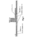
上述のように記憶蛍光体媒体の不透明な性質のために、励起光をプレートの正確な領域に閉じ込めることに関する従来技術の大きな問題が生じる。すなわち励起光は、不透明な蛍光体層内で水平方向に拡散する傾向にあり、そのため励起領域が不必要に増大する。この水平拡散効果は、従来の設計における問題であり、実際、本発明がその有効性を発揮する現象である。図1に示される本発明の具体的な実施形態によれば、記憶蛍光体板(storage-phosphor plate)102(プラスチック基板106上の記憶蛍光体層104を有する)の表面は、イメージング領域そのものではなく、イメージング領域(imaging area)に隣接する領域(すなわち検出器114の感光領域112の下の領域)において励起光108(例えば赤色光)に曝される。さまざまな実施形態によれば、励起光108は、単一のLEDまたはレーザペンシルビーム(例えば、画素毎の読み出し)、またはLEDアレイまたはレーザファンビーム(例えば、ライン毎の読み出し)の形で伝達される。特定の実施形態によれば、励起光に直接に曝される領域と、イメージング領域とは、プレート102の表面上の隣接した直線領域であり、検出器114は光検出器のリニアアレイである。 As described above, the opaque nature of the storage phosphor medium creates a major problem with the prior art relating to confining the excitation light in the correct area of the plate. That is, the excitation light tends to diffuse in the horizontal direction within the opaque phosphor layer, which unnecessarily increases the excitation region. This horizontal diffusion effect is a problem in the conventional design, and is actually a phenomenon in which the present invention exhibits its effectiveness. According to the specific embodiment of the invention shown in FIG. 1, the surface of the storage-phosphor plate 102 (having the storage phosphor layer 104 on the plastic substrate 106) is not in the imaging region itself. Rather, they are exposed to excitation light 108 (eg, red light) in an area adjacent to the imaging area (ie, the area below the photosensitive area 112 of the detector 114). According to various embodiments, the excitation light 108 is transmitted in the form of a single LED or laser pencil beam (eg, pixel-by-pixel readout), or LED array or laser fan beam (eg, line-by-line readout). The According to certain embodiments, the area directly exposed to excitation light and the imaging area are adjacent linear areas on the surface of the plate 102 and the detector 114 is a linear array of photodetectors.
図1に示される本発明の具体的な実施形態によれば、光検出器のリニアアレイは、励起光源が光検出器に隣接するプレートの領域を露光しているときに、プレートと接触するか、またはプレートに非常に近いところに位置しえる。光検出器のリニアアレイおよび励起光源は、光検出器のリニアアレイが先行し、励起光源が後に続いて、プレートを横切って同時に搬送される。光検出器のリニアアレイの下にあるプレートの領域は、拡散した励起光によって読み出され、具体的な実施形態ではその後、後続の励起光によって完全に消去される。 According to the specific embodiment of the present invention shown in FIG. 1, does the linear array of photodetectors contact the plate when the excitation light source is exposing an area of the plate adjacent to the photodetector? Or very close to the plate. The linear array of photodetectors and the excitation light source are simultaneously transported across the plate, followed by the linear array of photodetectors, followed by the excitation light source. The area of the plate under the linear array of photodetectors is read out by the diffuse excitation light, and in a specific embodiment is then completely erased by subsequent excitation light.
本発明のアプローチは、全ての励起光を集光(collect)できずに情報を失うことを恐れて、イメージング領域の外での励起をなくそうと一般に試みる従来技術とは反対である。本発明によればむしろ、イメージング領域に隣接する領域においてプレート102を励起することによって、イメージング領域は、励起光108に直接、曝されるのではなく、プレート内を水平に拡散する光116によって間接的に励起される。よって、プレート内の励起光の水平拡散に頼ることは、下部または上部からではなく、横からのプレートの領域の励起を可能にする。このようでなければ励起光がイメージング領域と同じ領域のプレートに入射するために必要な、プレートと検出器114との間のギャップをなくす(または最小化する)ことがこれでさらに可能になる。このように所望の領域を間接的に励起することで、検出器はイメージング領域に直接に接触する(または非常に距離が短い近傍に位置する)ことが可能となり、よって高い空間解像度とともに高い集光効率が得られる。 The approach of the present invention is contrary to the prior art, which generally attempts to eliminate excitation outside the imaging region, fearing that all excitation light cannot be collected and information is lost. Rather, according to the present invention, by exciting the plate 102 in a region adjacent to the imaging region, the imaging region is not directly exposed to the excitation light 108, but indirectly by light 116 that diffuses horizontally within the plate. Excited. Thus, relying on horizontal diffusion of the excitation light within the plate allows excitation of the region of the plate from the side rather than from the bottom or top. This further makes it possible to eliminate (or minimize) the gap between the plate and the detector 114 that would otherwise be necessary for the excitation light to enter the plate in the same region as the imaging region. Indirect excitation of the desired area in this way allows the detector to be in direct contact with the imaging area (or located in the vicinity of a very short distance) and thus with high spatial resolution and high concentration. Efficiency is obtained.
プレートの帯状の部分がプレートの一方から励起され、もう一方から画像取り込みがされる前述の設計とは異なり、この設計は特別な透明プレートを必要としない。むしろ従来の不透明な記憶蛍光体板を用いて実現できるのである。透明なプレートは高価で非常に製造が困難である一方、従来のプレートは製造が容易で簡単に入手できるという点で、これは大きな利点である。本発明の設計の他の利点は、励起するハードウェア(stimulating hardware)と集光するハードウェア(collecting hardware)とがプレートの同じ側上に配置できることである。そのような実施形態によれば、ハードウェアの全体的なプロファイルが非常に低くできる。そのようなある実施形態によれば(後述)、ハードウェアは、標準的なフィルムカセッテとほとんど同じ寸法の筐体の中に収まるように構成される。理解されるように、そのような実施形態は、プレートの対向する二つの側に配置される励起ハードウェアおよび集光ハードウェアを用いた場合は問題がある(かつ実用的ではない)。 Unlike the previous design where the strip of the plate is excited from one of the plates and the image is captured from the other, this design does not require a special transparent plate. Rather, it can be realized using a conventional opaque memory phosphor plate. This is a major advantage in that transparent plates are expensive and very difficult to manufacture, while conventional plates are easy to manufacture and readily available. Another advantage of the present design is that the exciting hardware and the collecting hardware can be located on the same side of the plate. According to such an embodiment, the overall hardware profile can be very low. According to one such embodiment (described below), the hardware is configured to fit within a housing that is approximately the same size as a standard film cassette. As will be appreciated, such an embodiment is problematic (and impractical) when using excitation and collection hardware located on two opposite sides of the plate.
記憶蛍光体板の同じ側上に励起ハードウェアおよび集光ハードウェアを配置することに関連したさらに他の利点は、励起ハードウェアを集光ハードウェアにアラインさせ、位置合わせすることに関連する。図2を参照して説明される具体的な実施形態によれば、励起および集光ハードウェアのセルフアラインされた機構(self-aligned assembly)が提供される。 Yet another advantage associated with placing the excitation and collection hardware on the same side of the storage phosphor plate is related to aligning and aligning the excitation hardware with the collection hardware. According to a specific embodiment described with reference to FIG. 2, a self-aligned assembly of excitation and collection hardware is provided.
図2は、励起光のためのセルフアラインされた構成を示す。すなわち光検出器のリニアアレイが、励起光がプレートに到達しないように遮断する。リニアアレイの端部が、励起光に直接曝されるプレートの領域と、拡散を通して間接的に励起光に曝されるプレートの領域との境界を定義する。より具体的には、リニアアレイ202は、その基板の端部にまで延びる感光領域204を有する。その端部に隣接するプレート206の領域は、励起光208に曝され、完全にアラインされ、よく制御された励起領域をリニアアレイ202の下に実現する。すなわち励起光208の幅がリニアアレイ202の左側の領域に限定されなくても、リニアアレイ202は励起光208についてナイフエッジのようにはたらき、アレイ202の感光領域204に隣接する直線領域だけが表面露出できるセルフアラインされたマスクを形成する。
FIG. 2 shows a self-aligned configuration for the excitation light. That is, the linear array of photodetectors blocks the excitation light from reaching the plate. The end of the linear array defines the boundary between the area of the plate that is directly exposed to the excitation light and the area of the plate that is indirectly exposed to the excitation light through diffusion. More specifically, the linear array 202 has a photosensitive region 204 that extends to the edge of the substrate. The area of the
感光領域204の下の励起された領域の幅は、プレートそれ自身の減衰係数とともに、プレートの露出領域における励起光208の強度による。例えばある媒体では、水平に拡散された励起光の強度は、露出領域の端部から離れるにつれ指数関数的に減少し、うまく定義できる。よって特定の媒体の特性および所望の解像度に依存して、励起光の強度および/またはリニアアレイのフォトサイト(photosite)は本発明の個々の応用例にしたがって変更されえる。本発明のそのような実施形態のセルフアラインされた性質に関する大きな利点は、例えばレーザファンビームを用いて励起光を注意深く焦点合わせすることが不要なことである。実際、照射される光は伝達されるうちに比較的広がってもよく、例えば安価なLEDアレイを用いることができる。 The width of the excited area under the photosensitive area 204 depends on the intensity of the excitation light 208 in the exposed area of the plate, along with the attenuation coefficient of the plate itself. For example, in some media, the intensity of the horizontally diffused excitation light decreases exponentially away from the edge of the exposed area and can be well defined. Thus, depending on the characteristics of the particular medium and the desired resolution, the intensity of the excitation light and / or the photosite of the linear array can be varied according to the particular application of the invention. A significant advantage with respect to the self-aligned nature of such embodiments of the present invention is that it is not necessary to carefully focus the excitation light using, for example, a laser fan beam. Actually, the irradiated light may be relatively spread while being transmitted, and for example, an inexpensive LED array can be used.
図1および図2は、本発明の基本原理を示す。しかし場合によっては、光検出器のリニアアレイを蛍光体板に接触させて配置することが現実的ではない。すなわち、リニアアレイの感光する側はしばしば相互接続するワイヤのボンディング領域を含む。これらのワイヤは典型的には感光面から突出していて、他の表面がそれに対して配置されることを不可能にする。これらのワイヤはまた非常に細く、切れやすいので、動く表面に直接接触することから保護されなければならない。リニアアレイ自身の感光面はまた、傷つきやすく、動く表面に直接接触することから保護されなければならない。ワイヤボンドおよび感光面の双方を保護する一つの方法には、光ファイバフェースプレートをリニアアレイの感光面と蛍光体板との間に用いることがある。そのような応用例においては、光ファイバのフェースプレートは、リニアアレイの感光面側に永久にボンディングされ、よってワイヤボンドが蛍光体板に触れないようにできる。図3は、水平に拡散した励起光に応答した誘導光の集光が光ファイバフェースプレート302を通して行われる具体的な実施形態を示す。記憶媒体304の表面と光ファイバフェースプレート302との間のギャップは図示のために強調されていることに注意されたい。 1 and 2 show the basic principle of the present invention. However, in some cases, it is not practical to place a linear array of photodetectors in contact with the phosphor plate. That is, the photosensitive side of the linear array often includes interconnecting wire bonding areas. These wires typically protrude from the photosensitive surface, making it impossible for other surfaces to be placed against it. These wires are also very thin and easy to break and must be protected from direct contact with moving surfaces. The photosensitive surface of the linear array itself is also sensitive and must be protected from direct contact with the moving surface. One way to protect both wire bonds and the photosensitive surface is to use an optical fiber faceplate between the photosensitive surface of the linear array and the phosphor plate. In such applications, the optical fiber faceplate is permanently bonded to the photosensitive surface side of the linear array, thus preventing wire bonds from touching the phosphor plate. FIG. 3 illustrates a specific embodiment in which the collection of guided light in response to horizontally diffused excitation light is performed through the fiber optic faceplate 302. Note that the gap between the surface of the storage medium 304 and the fiber optic faceplate 302 is highlighted for illustration.
図4は図3に示された構成がさらに発展したものを示す。図3において、光ファイバフェースプレートの端部は、プレートの直接露出された領域とプレートの間接的に露出された領域との境界を作る。この端部のシャープネスは、検出器アレイの下での拡散された光のプロファイルの均一さのために重要である。2つの光ファイバフェースプレートを互いに密着させて配置することで(一つは励起光を照射するために、一つは誘導光の集光のために)、集光フェースプレートの端部を欠けたり、ひび割れたりすることから保護することが可能である。この実施形態によれば、励起および集光機能の両方を実現する単一の装置が提供される。理解されるようにこの構成は、読み出し装置を記憶媒体といっしょに、例えば標準ラジオグラフィカセッテの中にパッケージングすることと同時に、励起および集光装置の同時走査を容易にする。 FIG. 4 shows a further development of the configuration shown in FIG. In FIG. 3, the end of the fiber optic faceplate creates a boundary between the directly exposed area of the plate and the indirectly exposed area of the plate. This edge sharpness is important for the uniformity of the diffused light profile under the detector array. By placing two optical fiber faceplates in close contact with each other (one for irradiating excitation light, one for condensing guided light), the end of the condensing faceplate may be chipped It can be protected from cracking. According to this embodiment, a single device is provided that implements both excitation and collection functions. As will be appreciated, this configuration facilitates simultaneous scanning of the excitation and collection devices while packaging the readout device with a storage medium, eg, in a standard radiographic cassette.
図示された実施形態において、検出器404のリニアアレイは、セラミックパッケージ406の中に、プラスチック基板414上の記憶蛍光体層412を持つ記憶蛍光体板410に励起光を与えるLED408の2次元アレイとともに統合されている。LED408からの励起光は、第1光ファイバフェースプレート416を介して蛍光体412の表面に伝送される。励起光が蛍光体412の表面へファイバを介して伝送されることは本発明の実施にはそれほど重要ではないので、代わりに、フェースプレート416は、ガラスまたはプラスチックのような均一な材料のブロックを有してもよい。
In the illustrated embodiment, a linear array of detectors 404 is combined with a two-dimensional array of LEDs 408 that provide excitation light to a
本発明のさまざまな実施形態を参照して上述したように、励起光は、検出器404の感光領域418の下の領域へと、蛍光体412の中で拡散して入り込む。蛍光体412のこの領域の間接的励起は、以前に記憶された情報が誘導光として放出することにつながり、この誘導光は検出器404によって第2光ファイバフェースプレート420を介して捕捉される。 As described above with reference to various embodiments of the present invention, the excitation light diffuses into the region below the photosensitive region 418 of the detector 404 in the phosphor 412. Indirect excitation of this region of the phosphor 412 leads to the emission of previously stored information as guided light, which is captured by the detector 404 via the second fiber optic faceplate 420.
前述の記載が参照する図には示されていないものとして、プレートによって拡散されて光検出器のリニアアレイへと向かう励起光を阻止または吸収するいくつかの手段がある。従来のレーザ走査方法のように、そのようなフィルタリングは適切なシステム動作のために重要である。すなわち、誘導光は励起光よりもずっと暗く、画像情報を含む唯一の光であるため、励起光が光検出器に到達するのを防ぐのは重要である。励起光を阻止するさまざまな技術が以下に説明される。 As not shown in the figures to which the above description refers, there are several means of blocking or absorbing the excitation light that is diffused by the plate and directed toward the linear array of photodetectors. As with conventional laser scanning methods, such filtering is important for proper system operation. That is, since the guide light is much darker than the excitation light and is the only light containing image information, it is important to prevent the excitation light from reaching the photodetector. Various techniques for blocking the excitation light are described below.
再び図4を参照して、励起光源と、放出されたエネルギーを後で捕捉する手段とが同じパッケージに配置されているので、これら2つの要素のアライメントは安定し、かつ信頼性がある。さらに記憶蛍光体板の表面にわたってLEDアレイおよび検出器が同時に協調して走査すること(図5に示されるように)は、例えば精密ステッピングモータのような単一の機構で処理できる。 Referring again to FIG. 4, since the excitation light source and the means for later capturing the emitted energy are located in the same package, the alignment of these two elements is stable and reliable. Furthermore, simultaneous and coordinated scanning of the LED array and detector across the surface of the storage phosphor plate (as shown in FIG. 5) can be handled by a single mechanism, such as a precision stepper motor.
図5は、例えばラジオグラフィシステムと用いられる画像データのキャプチャ(capturing)および読み出しのシステム500を示す。いったん画像が記憶媒体502(例えば記憶蛍光体板)にキャプチャされると、記憶された情報の放出およびキャプチャは、本発明に基づいて設計されたリニア読み出し装置504を記憶媒体502の表面にわたって走査することによって行われる。さまざまな実施形態によれば、読み出し装置は、図4を参照し前述した、励起光源および検出器アレイの両方が含まれる単一の装置を含みえる。あるいは装置504は、ここに説明するような方法での読み出しを実行するために、その動作および走査が密接に協調された2つの別個の装置を含みえる。
FIG. 5 shows a
すなわち装置504の特定の機械的性質に関係なく、記憶媒体502内の情報の読み出しは、上述の技術による注目領域の間接励起によって行われる。装置504の動きは、例えば精密ステッピングモータを含みえる機械アクチュエータ508を制御する信号を発生する走査制御506を介して制御されえる。理解されるように、正確に、例えばライン毎に、読み出し装置504を記憶媒体502にわたって走査するためのさまざまな技術が利用されえる。
That is, regardless of the specific mechanical properties of the
誘導光は記憶媒体502から放出され、後で取り出すために記憶されえる電気または光データに、キャプチャされた放射光を変換するさまざまな既知の技術によって、読み出し装置504の検出器によってキャプチャされる。506および510を介した走査制御および読み出し制御は、本発明の範囲から逸脱することなくさまざまな方法で実現できる。例えばそのような制御は、マイクロプロセッサ制御の回路、特定アプリケーション向け集積回路、またはソフトウェアを用いて実現できる。
Stimulated light is emitted from the
図6は、図5を参照して前述した読み出し装置および記憶媒体の組み合わせが、例えばラジオグラフィカセッテのような特定の応用のための標準サイズでありえるカセッテ602の中に一体化されえる本発明のさらに他の具体的な実施形態を示す。読み出し機構604の制御および記憶媒体605からのデータ読み出しは、商業的に入手可能なさまざまなパラレルまたはシリアルコネクタを含みえるコネクタ(不図示)を介して行える。あるいはデータ読み出しは、カセッテ602から外へ出る一つ以上の導体を介して行われてもよい。
FIG. 6 illustrates an embodiment of the present invention in which the reader and storage medium combination described above with reference to FIG. 5 can be integrated into a
ラジオグラフィの場合、そのようなデバイスは既に設置されたラジオグラフィシステムとともに用いられるほうが便利である。すなわち標準サイズのカセッテであれば、標準フィルムカセッテと同様にX線画像のキャプチャのための既存のラジオグラフィテーブルに挿入できる。画像データはそれから適当なコネクタ、例えばコネクタまたはコネクタ群の束を通して読み出され、一方、カセッテはその場での(in-situ)読み出しのためにラジオグラフィテーブルに装着されたまま残る。あるいはカセッテは取り出されて、リーダ(従来のPCまたはワークステーションでありえる)に接続されてもよい。記憶された情報の読み出し(および同時消去)はそれから前述のように行われ、その後、カセッテはその後の画像キャプチャに使えるようになる。 In the case of radiography, such a device is more conveniently used with an already installed radiography system. That is, a standard-size cassette can be inserted into an existing radiography table for capturing X-ray images in the same manner as a standard film cassette. The image data is then read through an appropriate connector, such as a bundle of connectors or groups of connectors, while the cassette remains mounted on the radiography table for in-situ readout. Alternatively, the cassette may be removed and connected to a reader (which can be a conventional PC or workstation). Reading (and simultaneous erasing) of stored information is then performed as described above, after which the cassette can be used for subsequent image capture.
さまざまな実施形態によれば、本発明は、その全体が全ての目的のためにここで参照によって援用される国際標準IEC 60406によって定義されるいかなる標準サイズのラジオグラフィカセッテに統合されて実施されてもよい。カセッテ寸法の具体例は、これには限定されないが、14インチ×17インチ、14インチ×14インチ、10インチ×12インチ、8インチ×10インチ、35cm×43cm、35cm×35cm、20cm×40cm、18cm×43cm、13cm×18cm、13cm×30cm、18cm×24cm、および24cm×30cmである。 According to various embodiments, the present invention is implemented in an integrated manner in any standard size radiographic cassette as defined by international standard IEC 60406, which is hereby incorporated by reference in its entirety for all purposes. Also good. Specific examples of cassette dimensions include, but are not limited to, 14 inches x 17 inches, 14 inches x 14 inches, 10 inches x 12 inches, 8 inches x 10 inches, 35 cm x 43 cm, 35 cm x 35 cm, 20 cm x 40 cm, They are 18 cm × 43 cm, 13 cm × 18 cm, 13 cm × 30 cm, 18 cm × 24 cm, and 24 cm × 30 cm.
画像データのキャプチャおよび処理の現状を考慮すると、標準の14インチ×17インチ画像のライン毎の走査は、本発明の技術を用いれば、おおよそ10秒で行え、従来のフィルム現像に必要な数分に比べて秀でている。さらに画像は電子的に記憶されるため、大きな現像済み画像を物理的に保管する必要なく、将来の取り出しに備えて永久に保存することができる。 Considering the current state of image data capture and processing, a standard 14-inch x 17-inch image line-by-line scan can be done in approximately 10 seconds using the technique of the present invention, a few minutes required for conventional film development. It is better than Furthermore, because the images are stored electronically, large developed images need not be physically stored and can be permanently stored for future retrieval.
カセッテ602のようなカセッテの中に統合された走査の特徴は、本発明の範囲から逸脱することなく改変できる。例えば上述のように、読み出し装置および機械走査機構はさまざまな形態を取りえる。さらに走査および読み出し制御のさまざまな部分はカセッテ602と統合されえる。例えば一つ以上のマイクロプロセッサおよびそれに付随する制御回路がカセッテ602の中に含まれて、外部コンピュータからの制御信号によって指示されるように走査および画像キャプチャを行ってもよい。さらに、画像を見たり、アーカイブしたりするためにダウンロードされるまでのあいだ一時的に画像を記憶するためのじゅうぶんなオンボードメモリを含むカセッテの中で、走査および画像キャプチャが完全に行われてもよい。
The scanning features integrated into the cassette, such as
あるいは走査および画像キャプチャの制御信号の発生は、完全にカセッテの外部で行われ、データが例えばコネクタを介してやりとりされてもよい。いずれにしても本発明は、走査(scanning)およびデータキャプチャ(data capture)機能のオンボードおよびオフボード制御のさまざまな組み合わせのいずれをも考慮し、かつ包含するものである。 Alternatively, the generation of scanning and image capture control signals may occur entirely outside the cassette, and data may be exchanged via, for example, a connector. In any event, the present invention contemplates and encompasses any of various combinations of on-board and off-board control of scanning and data capture functions.
ここまでで理解されるように、本発明の基本的な原理は、プレート内での励起光の水平拡散を通して記憶板の領域の励起を行うことにある。この基本原理に基づくシステムのパフォーマンスを改善するために、そのようなシステムの要素のそれぞれについて多く種類の最適化が行われえる。明らかになるように、これら最適化のいくつかはこの基本原理とは独立であり、よって独立した発明を構成する。このようなシステムのさまざまな構成要素がここで議論され、それらはストレージプレート、光ファイバフェースプレート、励起光のソース、光検出器のリニアアレイ、励起光を阻止するフィルタ、走査機構およびシステムハウジングを含む。 As understood so far, the basic principle of the present invention is to excite the region of the storage plate through the horizontal diffusion of the excitation light within the plate. In order to improve the performance of a system based on this basic principle, many types of optimization can be performed for each of the elements of such a system. As will become apparent, some of these optimizations are independent of this basic principle and thus constitute an independent invention. The various components of such a system are discussed here, including storage plates, fiber optic faceplates, excitation light sources, linear arrays of photodetectors, filters that block excitation light, scanning mechanisms and system housings. Including.
ストレージプレート(Storage plates)
ここで説明される励起(stimulation)および集光(collection)の方法は、従来のレーザ走査技術とは異なるので、本発明のために用いられるストレージプレートの物理的パラメータも異なりえる。すなわちプレートの厚さ、蛍光体の粒子の大きさ、結合剤の量、および色素の量は、本発明の技術の改良されたパフォーマンスのために、従来技術の場合に適切な値から変更されえる。
Storage plates
Since the methods of stimulation and collection described here are different from conventional laser scanning techniques, the physical parameters of the storage plate used for the present invention can also be different. That is, the thickness of the plate, the size of the phosphor particles, the amount of binder, and the amount of dye can be varied from values appropriate for the prior art due to the improved performance of the technology of the present invention. .
従来のレーザ走査技術によって読み出されるプレート中のエネルギー吸収色素のあるレベルの濃度を超えることは、そのような色素の高濃度のためにプレートの厚み全体にわたる励起ができなくなる傾向があるために、問題が起こりえる。それに対し本発明のさまざまな技術によれば、従来の技術によって引き起こされる不利益を伴うことなく、励起光の強度が単純に増加されえるので、非常に高い濃度のエネルギー吸収色素(energy-absorbing dye)を含むプレートを用いて、特定の吸収および励起特性を実現できる。 Exceeding a certain level of concentration of energy absorbing dye in a plate read out by conventional laser scanning techniques is problematic because the high concentration of such dye tends to prevent excitation across the thickness of the plate Can happen. In contrast, according to the various techniques of the present invention, the intensity of the excitation light can simply be increased without the disadvantages caused by the prior art, so that a very high concentration of energy-absorbing dye. Specific absorption and excitation properties can be achieved using a plate containing
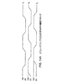
例えばストレージプレート中のエネルギー吸収色素(つまり励起光、例えば赤色光の波長において電磁エネルギーを吸収する色素)の量は、図7a〜図7cに示されるように励起光の水平拡散の量とプロファイルとを制御するために調節されえる。図7a〜図7cのグラフのそれぞれのペアは、モンテカルロシミュレーション法を用いてシミュレートされた、プレート中の赤色吸収色素の異なる濃度についての、赤色励起光(上のグラフ)の吸収プロファイル、および結果として生じる青い誘導光の点像分布関数を示す。それぞれのグラフにおける各グラデーションは10%の増分を表す。 For example, the amount of energy absorbing dye in the storage plate (i.e., the excitation light, e.g., the dye that absorbs electromagnetic energy at the wavelength of red light) is determined by the amount and profile of the horizontal diffusion of the excitation light as shown in Figs. 7a-7c. Can be adjusted to control. Each pair of graphs in FIGS. 7a-7c shows the absorption profiles of red excitation light (upper graph) and results for different concentrations of red absorbing dye in the plate, simulated using the Monte Carlo simulation method. The point spread function of the blue guided light generated as follows. Each gradation in each graph represents a 10% increment.
図7a〜図7cのグラフは、厚み全体にわたって同じエネルギーレベルでプレートを間接的に励起することが、ここで説明される技術で新たに可能になったことを示す。これらのグラフは、励起光が露出された端部から拡散してますます離れるにつれて、そのエネルギー分布がプレートの厚み全体にわたって均一になるという事実を示す。この現象は、非常に高い解像度を持ちながら、非常に高いX線吸収度も実現するX線画像システムを作るために利用されえる。 The graphs of FIGS. 7a-7c show that it is now possible with the techniques described herein to indirectly excite the plate at the same energy level throughout the thickness. These graphs show the fact that as the excitation light diffuses away from the exposed edge and gets further away, its energy distribution becomes uniform across the thickness of the plate. This phenomenon can be used to create an X-ray imaging system that has very high resolution while also achieving very high X-ray absorption.
非常に明るい照射を容易に実現できる(高出力赤色LEDの複数の列)ので、直接励起光強度のわずか10%で、プレート全体の消去(bleaching)を達成することが可能である。赤色光吸収色素が多いことで、プレートは、非常に狭い幅にわたりその厚み全体を通して読み出しすることができる。この構成は、高いX線吸収度(つまり高DQE)とともに高い解像度が必要となる乳房造影に特に有用である。したがってリニアCCDの方向にわたってよりも、機械的走査方向にわたってより高い解像度を達成することが理論的には可能である。 Since very bright illumination can easily be achieved (multiple rows of high-power red LEDs), it is possible to achieve bleaching of the entire plate with only 10% of the direct excitation light intensity. The high amount of red light absorbing dye allows the plate to read through its entire thickness over a very narrow width. This configuration is particularly useful for mammography where high resolution is required along with high X-ray absorption (ie, high DQE). It is therefore theoretically possible to achieve a higher resolution over the mechanical scanning direction than over the direction of the linear CCD.
リニアCCDの方向において、解像度は、誘導光とともに、励起光の水平拡散によって制限される。機械的走査の方向においては、解像度は励起光の水平拡散(赤色吸収色素の量によって制御されえる)によってのみ制限され、誘導光の水平方向の拡散によっては制限されない。光検出器の開口部(機械的走査の方向に沿った)は、解像度には影響を与えず、単に吸収効率に影響を与えるだけである。200μmの光検出器の開口部があれば、より細かい解像度(20μmにも及ぶ)を達成することができる。 In the direction of the linear CCD, the resolution is limited by the horizontal diffusion of the excitation light as well as the guide light. In the direction of mechanical scanning, the resolution is limited only by the horizontal diffusion of the excitation light (which can be controlled by the amount of red absorbing dye) and not by the horizontal diffusion of the guide light. The photodetector aperture (along the direction of mechanical scanning) does not affect the resolution, it only affects the absorption efficiency. With a 200 μm photodetector aperture, a finer resolution (up to 20 μm) can be achieved.
モンテカルロコンピュータシミュレーションを用いて、蛍光体粒子サイズ、赤色吸収色素濃度、およびプレート厚さを最適化して、特定の応用例についての最大のパフォーマンスを達成できる。この方法は、針状蛍光体(needle phosphor)技術に依存することなく、非常に高い解像度および高いX線吸収度を達成する大きな潜在能力を提供する。乳房造影に用いられる現在の製品や他の高解像度X線イメージングは、樹枝状蛍光体層(ヨウ化セシウムCsIの針状結晶)を用いて、放射された光をプレートの厚みにわたって通すようにしている。これらの蛍光体層は、非常に高価で製造が困難である。さらにこれらは非常に吸湿性が高く、問題を起こす画像焼き付き(image burn-in)(つまりX線に強く曝された針状蛍光体の領域は、周りの領域よりも高い発光ゲイン(luminous gain)を呈する)を呈する。 Monte Carlo computer simulation can be used to optimize phosphor particle size, red absorbing dye concentration, and plate thickness to achieve maximum performance for a particular application. This method offers great potential to achieve very high resolution and high X-ray absorption without relying on needle phosphor technology. Current products used for mammography and other high-resolution X-ray imaging use a dendritic phosphor layer (a cesium iodide CsI needle crystal) to allow the emitted light to pass through the thickness of the plate. Yes. These phosphor layers are very expensive and difficult to manufacture. In addition, they are very hygroscopic and cause image burn-in (that is, areas of acicular phosphors that are strongly exposed to X-rays have a higher luminous gain than surrounding areas). Present).
ここで説明された励起および集光方法を用いると、不透明記憶蛍光体板の機械的走査方向における解像度は、針状蛍光体プレートの解像度と同じくらい高くなりえる。高エネルギーX線をキャプチャするために、厚い記憶蛍光体板(つまり300μm)が用いられるときにおいてさえこれはあてはまる。 Using the excitation and collection methods described herein, the resolution of the opaque memory phosphor plate in the mechanical scan direction can be as high as the resolution of the needle-like phosphor plate. This is true even when a thick storage phosphor plate (ie 300 μm) is used to capture high energy X-rays.
図8に示される他の実施形態においては、記憶蛍光体の2層が同じ基板802上に堆積される。上部層804は少ない量の色素を含み、これは励起光を少しだけ吸収することを意味し、下部層806は多い量の色素を含み、これは励起光を多く吸収することを意味する。ここで説明される方法を用いてバイリニア(bilinear)光検出器アレイ808で走査されるとき、上部層804は下部層806よりも、直接の励起光暴露の端部からより遠くまで励起される。より具体的な実施形態によれば、上部層からの誘導光は、光検出器810である第1の列で集光され、一方、下部層からの誘導光は、光検出器812である第2の列で集光される。 In another embodiment shown in FIG. 8, two layers of storage phosphor are deposited on the same substrate 802. The top layer 804 contains a small amount of dye, which means that it absorbs a small amount of excitation light, and the bottom layer 806 contains a large amount of dye, which means it absorbs a lot of excitation light. When scanned with a bilinear photodetector array 808 using the method described herein, the upper layer 804 is excited farther from the edge of the direct excitation light exposure than the lower layer 806. According to a more specific embodiment, the guide light from the upper layer is collected in a first row that is a photodetector 810, while the guide light from the lower layer is a first detector that is a photodetector 812. Condensed in two rows.
さらに記憶蛍光体材料のX線吸収特性のために、上部層804は低いエネルギーのX線を吸収し、一方、下部層806は高いエネルギーのX線を吸収する。同様に柔らかい材料(人体の柔らかい組織など)は低いエネルギーのX線を優先的に吸収し、一方、密度の高い材料(人体の骨など)は高いエネルギーのX線を優先的に吸収する。したがって本発明の他の具体的な実施形態によれば、上部および下部層から集められた情報は、二重エネルギー画像(dual-energy image)を生成するのに用いられる。二重エネルギーデータはそれから、骨または軟組織だけに対応する情報を抽出するために処理されえる。さらに骨だけまたは軟組織だけを表示する画像が生成されえる。一般にさまざまな実施形態は、さまざまな記憶蛍光体材料の複数の層および複数の列からなる光検出器を用いて、二重エネルギーイメージングを実現する。 Further, due to the X-ray absorption characteristics of the storage phosphor material, the upper layer 804 absorbs low energy X-rays while the lower layer 806 absorbs high energy X-rays. Similarly, soft materials (such as soft tissues of the human body) preferentially absorb low energy X-rays, while dense materials (such as human bones) preferentially absorb high energy X-rays. Thus, according to another specific embodiment of the present invention, the information gathered from the upper and lower layers is used to generate a dual-energy image. The dual energy data can then be processed to extract information corresponding only to bone or soft tissue. In addition, an image can be generated that displays only bone or soft tissue. In general, various embodiments achieve dual energy imaging using photodetectors consisting of multiple layers and multiple columns of various storage phosphor materials.
従来は蛍光体板は、即発蛍光体スクリーン(prompt phosphor screens)のように可撓性基板(PET、Mylar(登録商標))上に製造される。これらのプレートは、搬送され、レーザ走査装置内で読み出しされるために、堅い裏板(例えばアルミ板)上にマウントされるか、または可撓性を保たれる。したがって、本発明の具体的な実施形態によれば、そのような可撓性のある蛍光体板の表面と、例えば光ファイバフェースプレートのような集光装置との間のじゅうぶんな接触を維持するために、蛍光体板は薄い発泡層(foam layer)上にマウントされ、集光装置がプレートの表面に押しつけられるときにこの発泡層が圧縮される。より具体的な実施形態によれば、集光装置がそれぞれの側で固定されるとき、発泡層がプレートの中央部では端部より厚くなりえ、これによりプレートの全体の幅にわたってじゅうぶんな接触を確実にする(例えば図9参照)。 Conventionally, phosphor plates are manufactured on flexible substrates (PET, Mylar®), such as prompt phosphor screens. These plates are mounted on a rigid back plate (eg, an aluminum plate) or kept flexible for transport and reading in a laser scanning device. Thus, according to a specific embodiment of the present invention, maintaining sufficient contact between the surface of such a flexible phosphor plate and a light collecting device, such as a fiber optic faceplate, for example. For this purpose, the phosphor plate is mounted on a thin foam layer, which is compressed when the light concentrator is pressed against the surface of the plate. According to a more specific embodiment, when the concentrator is fixed on each side, the foam layer can be thicker than the edges at the center of the plate, thereby providing sufficient contact over the entire width of the plate. Make sure (see, eg, FIG. 9).
光ファイバフェースプレート
さまざまな実施形態によれば、本発明による光ファイバフェースプレート(例えば図3および図4のプレート302および420)は2つの目的を達成する。すなわち励起光のためのナイフエッジアライメントを作り、読み出しを光検出器に集める。上述のように、フェースプレートのエッジが照射境界を定義し、そのシャープネスは最適化されたパフォーマンスを達成するのに重要である。光ファイバフェースプレートのエッジの物理的な完全性(physical integrity)を保護するために、他のフェースプレートがそれに対向するようにマウントされえる(例えば図4のプレート416)か、あるいは、透過材料の透明ブロック(例えばガラスまたはプラスチック)がそれに対向してマウントされえる。材料の選択は励起光に必要なコリメーションの量に依存する。もし追加のコリメーションが不要なら、透明な材料が用いられえる。もし追加のコリメーションが必要なら、他の光ファイバフェースプレートが励起光をプレートに伝送するのに用いられえる。理解されえるように、追加のコリメーションの量は光ファイバフェースプレートの開口数によって決定される。もし低い開口数が選ばれるなら、プレートを打つ励起光は高くコリメートされる。集光フェースプレートに対向してマウントされたブロックの性質にかかわらず、集光フェースプレートの端部は、動作中の欠けや他のダメージに対して保護される。
Fiber Optic Faceplate According to various embodiments, fiber optic faceplates according to the present invention (eg, plates 302 and 420 in FIGS. 3 and 4) accomplish two purposes. That is, a knife edge alignment for the excitation light is created and the readout is collected on a photodetector. As mentioned above, the faceplate edge defines the illumination boundary, and its sharpness is important to achieve optimized performance. In order to protect the physical integrity of the edge of the fiber optic faceplate, another faceplate can be mounted opposite it (eg plate 416 in FIG. 4) or the transmission material A transparent block (eg glass or plastic) can be mounted opposite it. The choice of material depends on the amount of collimation required for the excitation light. Transparent materials can be used if no additional collimation is required. If additional collimation is required, other fiber optic faceplates can be used to transmit the pump light to the plate. As can be appreciated, the amount of additional collimation is determined by the numerical aperture of the fiber optic faceplate. If a low numerical aperture is chosen, the excitation light striking the plate will be highly collimated. Regardless of the nature of the block mounted opposite the collection faceplate, the end of the collection faceplate is protected against chipping and other damage during operation.
具体的な実施形態によって、光検出器のリニアアレイ上へのマウントを容易にするために、光ファイバフェースプレートは図4に示されるようにファイバの方向に対してわずかに角度をつけて切断されえる。このようなわずかなバイアスは、伝送特性を大きく減少させることなく、例えば10度未満のバイアスカット角なら10%の伝送減少に収めて、伝達フェースプレートをリニアアレイ上に容易にアラインさせることができる。 In accordance with a specific embodiment, the fiber optic faceplate is cut at a slight angle with respect to the direction of the fiber as shown in FIG. 4 to facilitate mounting the photodetector on a linear array. Yeah. Such a slight bias can easily align the transmission faceplate on the linear array without greatly reducing the transmission characteristics, for example, with a bias cut angle of less than 10 degrees, with a transmission reduction of 10%. .
本発明の他の具体的な実施形態によれば、集光(collection)光ファイバフェースプレートはまた他の重要な目的も果たす。すなわち、それは部分的にまたは完全に励起光を阻止するように構成されえる。そのような阻止を行うために、光ファイバフェースプレートは励起光を吸収し、誘導光を伝送する材料で構成されえる。そのような材料は、イオン色ガラス(ionically colored glass)、例えばSchott BG3のような光学フィルタ材料を含む。しかしそのような材料をファイバに伸ばしてそれらを光ファイバフェースプレートに束ねることは困難を伴う(例えばそのようなガラスは低屈折率を有し、さまざまな熱処理を通して安定ではない)ために、そのような応用には最良の材料にならない。 According to other specific embodiments of the present invention, the collection fiber optic faceplate also serves other important purposes. That is, it can be configured to partially or completely block excitation light. To perform such blocking, the fiber optic faceplate can be constructed of a material that absorbs the pumping light and transmits the guiding light. Such materials include optical filter materials such as ionically colored glass, eg, Schott BG3. However, it is difficult to stretch such materials into fibers and bundle them into fiber optic faceplates (eg, such glasses have a low refractive index and are not stable through various heat treatments). It is not the best material for any application.
希土類でドーピングされたフィルタガラスのような他の材料が、光ファイバフェースプレートのよりよい候補である。もともろその蛍光特性のために開発された希土類でドーピングされたフィルタガラスは、フィルタ材料としても用いられえる。特に、ツリウムがドーピングされたガラスは、400nmにおいて良好な伝送特性を、680nmにおいて良好な吸収特性を有する。よって本発明の具体的な実施形態によれば、低い屈折率のホストガラス(low index host glass)および高い屈折率のホストガラスはツリウムでドーピングされ、クラッドおよびコア材を形成する。これらのコアおよびクラッド材はそれから束ねられ、本発明に用いられる良好な伝送特性(つまり高い開口数)および励起光のじゅうぶんな阻止性能を持つ光ファイバフェースプレートを形成する。 Other materials such as filter glasses doped with rare earths are better candidates for fiber optic faceplates. Of course, the rare earth-doped filter glass developed for its fluorescent properties can also be used as a filter material. In particular, glass doped with thulium has good transmission characteristics at 400 nm and good absorption characteristics at 680 nm. Thus, according to a specific embodiment of the present invention, the low index host glass and the high index host glass are doped with thulium to form the cladding and core material. These core and clad materials are then bundled to form an optical fiber faceplate with good transmission characteristics (ie high numerical aperture) and sufficient pump light blocking capability used in the present invention.
よく知られるように、光ファイバフェースプレートの伝送は、それぞれのファイバの開口数の関数である。それぞれのファイバの開口数は、コアおよびクラッド材間の屈折率の差が大きくなるほど、大きくなる。光ファイバフェースプレートは、高い屈折率および低い屈折率の材料が容易に得られるので、従来はガラスから製造されている。これはプラスチック材料の場合にはあてはまらなかった。すなわちたいていのプラスチック材料は1.4に近い屈折率を有する傾向がある。新しいプラスチック材料がフロリダベースの会社、Optical Polymer Research Inc.から商業的に入手可能となった。最近までたいていの光ファイバフェースプレートは、じゅうぶんな屈折率の差がある材料を容易に得られるため、ガラスから製造されてきた。最近、新しいクラスのプラスチック材料が開発された。Opti−Cladという名で販売されているこの新しい材料は、非常に低い屈折率(1.36未満)を持ち、そのため例えばスチレンコア(styrene core)(屈折率が1.59に近い)の周りのクラッド材として用いるのに適している。屈折率が1.3であるためテフロン(登録商標)もまた良好なクラッド材である。材料科学のこのような発展のおかげで、今や高い開口数を持つプラスチックの光ファイバフェースプレートを製造することができる。本発明の具体的な実施形態によれば、そのような光ファイバフェースプレートが高い開口数および良好な励起光阻止を実現するために、使用されるプラスチックにエネルギー吸収色素が入れられる。 As is well known, the transmission of a fiber optic faceplate is a function of the numerical aperture of each fiber. The numerical aperture of each fiber increases as the difference in refractive index between the core and the cladding material increases. Fiber optic faceplates are conventionally made from glass because materials with high and low refractive indices are easily obtained. This was not the case with plastic materials. That is, most plastic materials tend to have a refractive index close to 1.4. The new plastic material is a Florida-based company, Optical Polymer Research Inc. Became commercially available. Until recently, most fiber optic faceplates have been manufactured from glass because it is easy to obtain materials with substantial refractive index differences. Recently, a new class of plastic materials has been developed. This new material sold under the name Opti-Clad has a very low refractive index (less than 1.36), for example around styrene core (with a refractive index close to 1.59). Suitable for use as a cladding material. Since the refractive index is 1.3, Teflon is also a good cladding material. Thanks to this development in material science, it is now possible to produce plastic optical fiber faceplates with a high numerical aperture. In accordance with a specific embodiment of the present invention, in order for such a fiber optic faceplate to achieve a high numerical aperture and good pump light rejection, an energy absorbing dye is incorporated into the plastic used.
励起光を阻止する他のアプローチは、反射(屈折ではなく)クラッド材を光ファイバフェースプレートのファイバに使うことを伴う。そのようなファイバは、反射するたびにエネルギー損失をするので長距離にわたる光エネルギーの伝送には理想的なものではない。しかし本発明のたいていの実現例において想定される短い距離(例えば1インチ未満)の場合、そのようなファイバはじゅうぶんに伝送しやすいといえる。 Another approach to blocking the pump light involves using a reflective (rather than refractive) cladding material for the fiber of the fiber optic faceplate. Such a fiber is not ideal for transmitting light energy over long distances because it loses energy each time it is reflected. However, for short distances assumed in most implementations of the present invention (eg, less than 1 inch), such a fiber can be said to be well transmitted.
上述のように様々な実施形態によれば、光ファイバフェースプレートは、励起光のためのナイフエッジを作るために、誘導光を集光し、光検出器上に結像させる(imaging)ために、さらに励起光が光検出器に到達するのを防ぐために、有用でありえる。しかし本発明を実施するのに、光ファイバフェースプレートを用いずに済ませることもできる(図1および図2に示されるように)。 As described above, according to various embodiments, the fiber optic faceplate collects the guide light and images it onto the photodetector to create a knife edge for the excitation light. Furthermore, it may be useful to prevent excitation light from reaching the photodetector. However, it is possible to dispense with the use of a fiber optic faceplate to implement the present invention (as shown in FIGS. 1 and 2).
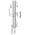
またイメージプレートおよび光検出器の間に平らで透明な層(ガラスまたはプラスチック材料)を置いて、ボンディングワイヤがイメージプレートに触れないようにすることもできる。もしなんの予防策も採られないなら、イメージプレートがランバート放射体であり、誘導光が光検出器に到達する前に透明層内で全ての方向に拡散するという事実のために、そのような透明な層は、許容できないくらいの量のボケ(blurring)を生じるだろう。一方で、ボケを防止するために透明層の厚さは最小に抑えられなければならず、他方で、ボンディングワイヤのためにプレートと光検出器との間に必要な間隔を提供するために、層はじゅうぶん厚くなければならない。本発明の具体的な実施形態によれば、多くの技術を独立に、または組み合わせて用いて適正な妥協点に到達することができる。 It is also possible to place a flat and transparent layer (glass or plastic material) between the image plate and the photodetector so that the bonding wires do not touch the image plate. If no precautions are taken, due to the fact that the image plate is a Lambertian emitter and the guided light diffuses in all directions within the transparent layer before reaching the photodetector, such A transparent layer will produce an unacceptable amount of blurring. On the one hand, the thickness of the transparent layer has to be minimized in order to prevent blurring, on the other hand, in order to provide the necessary spacing between the plate and the photodetector for the bonding wire, The layer should be thick enough. In accordance with a specific embodiment of the present invention, a number of techniques can be used independently or in combination to reach a reasonable compromise.
そのような第1の技術によれば、リニアアレイの光検出器領域上で薄く、リニアアレイのボンディングエリア上で厚い傾斜した透明層が用いられる。これはリニアアレイがイメージプレートと平行に位置しないことを意味する。図10bに示されるように、リニアアレイ1002は、光検出器領域1006がプレートにより近く、ボンディング領域がプレートからより遠いようにプレート1004に対して角度をつけて配置される。この手法を使えば、透明層1008の厚さを、光検出器領域上では最小化し、ボンディング領域上では最大化することができる。
According to such a first technique, an inclined transparent layer is used that is thin on the photodetector area of the linear array and thick on the bonding area of the linear array. This means that the linear array is not located parallel to the image plate. As shown in FIG. 10b, the linear array 1002 is angled with respect to the
より具体的な実施形態によれば、リニアアレイは空洞(cavity)の中に置かれ、液体の透明エポキシがリニアアレイの上から流し込まれる。いったんエポキシが硬化すると、それは堅い透明層を作り、光検出器領域上では薄く、リニアアレイのボンディング領域上では厚くなる。ボンディングワイヤは、このエポキシによって直接に封止されるか、またはエポキシで覆われる前にまず柔軟な材料(例えばシリコーン)でコーティングされることによって熱膨張係数の不整合に関連する問題を軽減するかされる。プレートと接触するエポキシの表面が完全に平らになることを確実にするために、エポキシが満たされるモールドを使うことが提案される。例えばモールドは、エポキシが注がれるあいだエポキシを蓄え、エポキシが硬化した後に取り除かれる、リニアアレイの前に配置される完全に平らなテフロン(登録商標)コーティングされた表面のかたちで簡単には実現できる。ある実施形態によれば、Ablestickによって製造される4021Tのような1液形エポキシが用いられえる。このエポキシはガラスおよびシリコンには固着するが、テフロンコーティングされた表面には接着しない。透明エポキシはまた、励起光を阻止する吸収色素を含みえる(本明細書で後述)。 According to a more specific embodiment, the linear array is placed in a cavity and a liquid transparent epoxy is poured over the linear array. Once the epoxy is cured, it creates a rigid transparent layer that is thin on the photodetector area and thick on the bonding area of the linear array. Will the bonding wire be sealed directly with this epoxy or may be first coated with a flexible material (eg silicone) before being covered with epoxy to reduce problems associated with thermal expansion coefficient mismatches? Is done. In order to ensure that the surface of the epoxy in contact with the plate is completely flat, it is proposed to use a mold filled with epoxy. For example, the mold is easily realized in the form of a completely flat Teflon-coated surface that is placed in front of a linear array that stores the epoxy while it is poured and is removed after the epoxy has cured. it can. According to one embodiment, a one-part epoxy such as 4021T manufactured by Ablestick can be used. This epoxy adheres to glass and silicon but does not adhere to Teflon coated surfaces. Transparent epoxies can also include an absorbing dye that blocks excitation light (described later herein).
図10aに示される第2の技術は、高い屈折率材料(n〜1.6)からできた透明な層1022を用いることを伴う。プレート1024から放射される光は、高屈折率材料1022内で、法線方向の入射角(normal incidence)に対してより小さい角度で屈折する(スネルの法則)。結果として生じるボケがこれで減少する。
The second technique shown in FIG. 10a involves using a transparent layer 1022 made of a high refractive index material (n˜1.6). Light emitted from the
図10cに示される第3の技術は、干渉フィルタ1042を透明な層1044の表面上にイメージプレート1046と接触するように堆積させることを含む。干渉フィルタの目的は、法線方向の入射に近い角度でフィルタに到達する、プレートによって放射された誘導光を伝送し、ある角度以上でフィルタに到達する誘導光をプレートへと反射して戻すことである。このタイプの干渉フィルタは、前方ピーキング分布を作るため、つまり前方方向の光放射の強度を増し、軸からはずれた向きの強度を減少させるために即発放出蛍光体(prompt-emitting phosphors)の前に用いられる。この技術は特に、CRT蛍光体スクリーンおよびプロジェクションレンズ(例えば大画面TVにおける)間、または即発放射蛍光体およびレンズベースのカメラ間の光結合を最大化するのに有用である(Norikata Satoh、 SPIE volume 2432、462〜469ページ)。この技術は空間解像度を犠牲にして前方方向への光放射の強度を増す。この技術は、より多くの光を集める目的のためではなく、ボケの効果に大きく関わる軸からずれた光を阻止する目的で本発明において用いられる。
A third technique shown in FIG. 10 c includes depositing interference filter 1042 on the surface of
リニアアレイ上にどの材料が用いられるかにかかわらず(例えば光ファイバフェースプレート、ガラス、プラスチック、またはエポキシ層)、この材料はイメージプレートに傷をつけてはいけない。ホコリや汚れを接触領域から取り除くことが傷がつく可能性を減らす。特定の実施形態においては、テフロンのようなさらなる層がプレート上にコーティングされるか、またはその材料そのものが用いられ、2つの表面間の摩擦を減らす。他の特定の実施形態においては、イメージプレートと接触する表面の外側の端部は傾斜がつけられるか、または丸みがつけられて傷がつく可能性を減らす。 Regardless of which material is used on the linear array (eg, fiber optic faceplate, glass, plastic, or epoxy layer), this material should not damage the image plate. Removing dust and dirt from the contact area reduces the chance of scratching. In certain embodiments, an additional layer, such as Teflon, is coated on the plate, or the material itself is used to reduce friction between the two surfaces. In other specific embodiments, the outer edge of the surface that contacts the image plate is beveled or rounded to reduce the possibility of scratching.
励起光の光源
励起光の光源が、互いに近接してマウントされた発光ダイオード(LED)群の列を含む本発明の様々な実施形態がここで説明されてきた。そのようなLEDアレイは商業的に入手可能であり、例えばStockerYale linelightsがある。そのようなモジュールの例では、100mmの基板上にLEDのそれぞれの間に1mmの間隔を空けて100個のLEDチップが直接マウントされている。典型的なLEDアレイの全体の照度はアレイの長手方向にわたってかなり均一である。本発明で提案される光励起方法の利点の一つは、プレートの深さ全域を消去(bleach)するのにじゅうぶんなだけ高い照度を確保することによって、アレイの長手方向にわたる照度のバラツキに対して比較的左右されないことである。ある実施形態によれば、この閾値に達成することは、ひとつ以上のさらなるLEDの列を第1の列に追加することによって確実になり、これによってプレート上の励起光の量を増すことができる。
Excitation Light Source Various embodiments of the present invention have now been described in which the excitation light source includes an array of light emitting diodes (LEDs) mounted in close proximity to each other. Such LED arrays are commercially available, for example StockerYale linelights. In an example of such a module, 100 LED chips are directly mounted on a 100 mm substrate with a 1 mm spacing between each of the LEDs. The overall illumination intensity of a typical LED array is fairly uniform over the length of the array. One of the advantages of the photoexcitation method proposed in the present invention is that it ensures a high enough illuminance to bleach the entire depth of the plate, thereby avoiding variations in illuminance across the length of the array. It is relatively unaffected. According to certain embodiments, achieving this threshold can be ensured by adding one or more additional LED columns to the first column, which can increase the amount of excitation light on the plate. .
具体的な実施形態によれば、LEDのピーク発光波長は、プレートおよび光検出器の間に置かれたフィルタのピーク吸収波長と一致する。さらにLEDは、フィルタの実効吸収範囲よりも狭い発光スペクトルを有するように選ばれる。これがあてはまらないある実施形態においては、追加のフィルタがLEDおよびプレート間に加えられる。この追加フィルタの目的は、プレートおよび光検出器間の1次フィルタによって阻止されない励起光のいかなる波長をも阻止することにある。他の実施形態においては、LEDの明るさを調整する制御回路が提供される。制御回路は、プレートの部分消去(partial bleaching)を実現するためにLEDの明るさを低減するために用いられえる。 According to a specific embodiment, the peak emission wavelength of the LED matches the peak absorption wavelength of a filter placed between the plate and the photodetector. In addition, the LEDs are selected to have an emission spectrum that is narrower than the effective absorption range of the filter. In certain embodiments where this is not the case, an additional filter is added between the LED and the plate. The purpose of this additional filter is to block any wavelength of excitation light that is not blocked by the first order filter between the plate and the photodetector. In another embodiment, a control circuit for adjusting the brightness of the LED is provided. The control circuit can be used to reduce the brightness of the LED to achieve partial bleaching of the plate.
さらに他の実施形態によれば、より大きい消去効率を実現するために異なる色のLEDの列がさらに設けられる。単色照射よりも広帯域照射のもとで記憶蛍光体板がより効率よく消去されることが示されている。したがって紫外、青、緑、黄、橙または赤外LED群のさらなる列を赤色LED群の列に追加することが、広帯域照射を模擬し、消去効率を増すために提案される。 According to yet another embodiment, an array of LEDs of different colors is further provided to achieve greater erase efficiency. It has been shown that the storage phosphor plate is erased more efficiently under broadband illumination than with monochromatic illumination. Therefore, adding an additional row of ultraviolet, blue, green, yellow, orange or infrared LED groups to the row of red LED groups is proposed to simulate broadband illumination and increase erase efficiency.
また、二段階消去法を用い、いくつかの記憶蛍光体板がより効率的に消去されることが示されている。そのような二段階消去法は、Fuji Computer Radiography Technical ReviewのNo. 2(「FRC9000における新しい技術開発」)の18ページに記載される。それはプレートを第1段階として紫外光に曝し、そして第2段階として紫外光なしで広帯域照射に曝す。Fujiは、プレートを高輝度蛍光管群のスタック上を通すことによってこの方法を実現し、ここでは蛍光管のいくつかは直接にプレートを露光し、いくつかは紫外線除去フィルタで覆われている。 It has also been shown that some storage phosphor plates can be erased more efficiently using a two-stage erase method. Such a two-stage erasure method is described on page 18 of Fuji Computer Radiography Technical Review No. 2 (“New Technology Development in FRC9000”). It exposes the plate to ultraviolet light as the first stage and to broadband irradiation without ultraviolet light as the second stage. Fuji achieves this method by passing the plate over a stack of high-intensity fluorescent tube groups, where some of the fluorescent tubes directly expose the plate and some are covered with UV-removing filters.
本発明の具体的な実施形態は、二段階消去法を新しい方法で導入する。蛍光管群はLEDの列で置き換えられる。第1消去段階は、紫外LEDだけを用いて構築される。紫外LEDは今では多くのメーカから商業的に入手可能である(例えば日亜NSHU-550EまたはNSHU-590E)。これらのLEDは、370nmから375nmの間でほぼ1mWを出力する。これらはまた可視出力が非常に低く(かすかな紫の光)、容易にフィルタで除去できる。第2消去段階は、紫外光を作り出さない様々な他の色のLED群を用いて構築できる。 Specific embodiments of the present invention introduce a two-step erase method in a new way. The group of fluorescent tubes is replaced with a row of LEDs. The first erase stage is constructed using only ultraviolet LEDs. Ultraviolet LEDs are now commercially available from many manufacturers (eg Nichia NSHU-550E or NSHU-590E). These LEDs output approximately 1 mW between 370 nm and 375 nm. They also have very low visible output (faint purple light) and can be easily filtered out. The second erase stage can be constructed using a variety of other colored LEDs that do not produce ultraviolet light.
光検出器のリニアアレイ
本発明で用いられる光検出器のリニアアレイ(例えば上述のアレイ114、202、および404)は、様々な異なる方法によって組み立てられる。例えばディスクリートの(個別の;discrete)光検出器群が一つの列にマウントされ、マルチプレクス回路に接続される。あるいは光検出器のアモルファスシリコンアレイが使用されえる。低雑音読み出しを実現するために、単結晶シリコン基板に設けられた光検出器群が好ましい。このようなリニアアレイは、電荷結合素子(CCD)またはCMOS技術を用いて製造されえる。イメージセンサのためのCMOS技術は、この数年で飛躍的に発達し、CMOSイメージセンサのパフォーマンス特性はCCDのそれに近づいている。本発明は、利用可能なあらゆる種類の光検出器技術を排除するものではない。リニアCCDのパフォーマンスに基づいて本発明の様々な実施形態はさらなる改善を提供するものであり、それが後述される。
Photodetector Linear Array The photodetector linear array used in the present invention (eg, the arrays 114, 202, and 404 described above) is assembled in a variety of different ways. For example, discrete (discrete) photodetectors are mounted in a row and connected to a multiplex circuit. Alternatively, an amorphous silicon array of photodetectors can be used. In order to realize low-noise readout, a group of photodetectors provided on a single crystal silicon substrate is preferable. Such linear arrays can be manufactured using charge coupled device (CCD) or CMOS technology. CMOS technology for image sensors has developed dramatically over the past few years, and the performance characteristics of CMOS image sensors have approached those of CCDs. The present invention does not exclude all types of photodetector technology available. Based on the performance of linear CCDs, various embodiments of the present invention provide further improvements, which are described below.
従来のリニアCCDは、光検出器としてフォトダイオードまたは接合ゲートに頼っている。いずれの設計も、スペクトルの青色領域においては高い量子効率(ほぼ60%)を持つ光検出器を提供するが、これはこれら光検出器が、レジスタに用いられるポリシリコンゲート(青色でよく吸収する)によって覆われていないからである。今日のリニアCCDの内部(intrinsic)量子効率は、理論限界値に近い。しかし、シリコン表面で反射される光の量が多いために外部(extrinsic)量子効率は低い。これはまた、シリコンの屈折率が高いという事実による。無反射コーティングを使用することで、背面照射エリアCCD(back-illuminated area CCD)の量子効率を改善する試みが成功している。しかし従来の前面照射リニアCCD(front-illuminated linear CCD)の量子効率を改善するためのいかなる類似の努力も、製品や文献に報告されてきていない。したがって本発明は、リニアCCDに無反射コーティング(antireflection coatings)を提供することで、シリコン表面から反射される量を低減する。前面照射型リニアCCDの量子効率を多層コーティング(例えば酸化ハフニウム)を用いることで400nm(例えば誘導光の波長)において60%から95%に改善できる。さらに、そのような多層コーティングはまた、650nm(励起光の波長)の光を反射することによって、前面照射型リニアCCDの量子効率を80%から1%に低減できる。すなわちこれらの多層コーティングは、励起光のための阻止フィルタとして、かつ誘導光のための無反射層としてふるまうように実現できる。 Conventional linear CCDs rely on photodiodes or junction gates as photodetectors. Both designs provide photodetectors with high quantum efficiency (nearly 60%) in the blue region of the spectrum, which are the polysilicon gates used in the resistors (blue absorbs well) ) Because it is not covered by The intrinsic quantum efficiency of today's linear CCD is close to the theoretical limit. However, extrinsic quantum efficiency is low due to the large amount of light reflected at the silicon surface. This is also due to the fact that the refractive index of silicon is high. Attempts to improve the quantum efficiency of back-illuminated area CCDs by using anti-reflective coatings have been successful. However, no similar effort has been reported in the product or literature to improve the quantum efficiency of conventional front-illuminated linear CCDs. Accordingly, the present invention reduces the amount reflected from the silicon surface by providing antireflection coatings on the linear CCD. The quantum efficiency of a front-illuminated linear CCD can be improved from 60% to 95% at 400 nm (for example, the wavelength of induced light) by using a multilayer coating (for example, hafnium oxide). Furthermore, such multilayer coatings can also reduce the quantum efficiency of front-illuminated linear CCDs from 80% to 1% by reflecting light at 650 nm (excitation light wavelength). That is, these multilayer coatings can be implemented to act as blocking filters for excitation light and as non-reflective layers for guided light.
前述のように、従来のリニアCCDは、光検出器としてフォトダイオードまたは接合ゲートに依存する。そのようなフォトダイオードまたは接合ゲート光検出器を作るためには、追加プロセスのステップが必要であり、コストおよびCCD製造プロセスの複雑さが増す。より容易で安価なプロセスは、フルフレームエリアCCD(full-frame area CCD)に使われるような、リニアCCDを製造ために用いられるが、それは青色量子効率を犠牲にした上でのことである。フルフレームエリアCCDは、垂直レジスタが光検出器としてはたらく簡単な製造プロセスを用いる。これらはスペクトルの青領域で低い量子効率(ほぼ10%)を呈するが、これは垂直レジスタがこれらの波長で強い吸収を見せるポリシリコンゲートで覆われているからである。ポリシリコンゲートを薄くするか、またはそのようなゲートを光検出器領域の部分から取り除くことによって青色量子効率を増す試みがなされてきた。 As described above, a conventional linear CCD relies on a photodiode or junction gate as a photodetector. To make such a photodiode or junction gate photodetector requires additional process steps, increasing cost and complexity of the CCD manufacturing process. An easier and less expensive process is used to manufacture linear CCDs, such as those used for full-frame area CCDs, at the expense of blue quantum efficiency. Full frame area CCDs use a simple manufacturing process in which a vertical register acts as a photodetector. They exhibit low quantum efficiency (almost 10%) in the blue region of the spectrum because the vertical register is covered with a polysilicon gate that exhibits strong absorption at these wavelengths. Attempts have been made to increase blue quantum efficiency by thinning polysilicon gates or removing such gates from portions of the photodetector area.
したがって本発明の具体的な実施形態によれば、従来のフルフレームエリアCCDプロセスを用いて製造されたリニアCCDの青色量子効率を増す技術が導入される。提案される光検出器のレイアウトは、広いチャネルストップ領域群(ポリシリコンゲートによって覆われない)に両側で囲まれた狭いポリシリコンゲート(つまりフォトゲート)を含む。この光検出器の設計は、従来のリニアCCD光検出器とは劇的に異なるが、それは光検出器群の間のチャネルストップ領域が光検出器それ自身よりもずっと広い(図11aおよび図11bで比較されたい)からである。 Thus, according to a specific embodiment of the present invention, a technique is introduced that increases the blue quantum efficiency of a linear CCD fabricated using a conventional full frame area CCD process. The proposed photodetector layout includes a narrow polysilicon gate (ie photogate) surrounded on both sides by a wide channel stop region group (not covered by a polysilicon gate). This photodetector design is dramatically different from conventional linear CCD photodetectors, but it has a much wider channel stop region between photodetectors than the photodetectors themselves (FIGS. 11a and 11b). Because I want to compare with.)
従来は、狭いチャネルストップ領域1102が光検出器1104の間に埋め込まれ、それらの間に鋭いポテンシャル障壁を形成する(図11a)。チャネルストップ領域は高い量子効率を呈するが、強い電界はないので、その領域で発生した電子は水平方向に拡散し、2つの隣接する光検出器のどちらかの側に逃げる。たいていのリニアCCD設計においてチャネルストップ幅は、光検出器群の間での鋭い分離をできるだけ作るために最小に抑えられ、そのためコントラスト(つまりMTF)が増大する。光検出器の応答は、台形のカーブで表現でき、もしチャネルストップ部が光検出器に比べ狭いと四角形に近づく(図12a)。 Conventionally, a narrow channel stop region 1102 is embedded between the photodetectors 1104, forming a sharp potential barrier between them (FIG. 11a). The channel stop region exhibits high quantum efficiency, but there is no strong electric field, so electrons generated in that region diffuse horizontally and escape to either side of two adjacent photodetectors. In most linear CCD designs, the channel stop width is minimized to create as much sharp separation as possible between the photodetectors, thus increasing the contrast (ie, MTF). The response of the photodetector can be expressed by a trapezoidal curve, and approaches a square if the channel stop is narrower than the photodetector (FIG. 12a).
これに対して本発明の具体的な実施形態によれば、チャネルストップ1152は、光検出器1154よりも広い(図11b)ので、三角形の形の光検出器応答カーブを描く(図12b)。図からわかるように、これは隣接光検出器の間の分離を低減する(すなわち重複した応答を発生する)。より具体的な実施形態によれば、この効果は、光検出器を必要な解像度よりも細かいピッチで設け、それらの信号をCCDレジスタの出力において(アナログビニング技術)、またはそれらが2値化されたあとに(図12c)結合することによって緩和される。この設計は、青色量子効率を高める本来の目的を達成するだけでなく、チャネルストップ領域はCCDチャネルよりも少ししか暗電流を発生しないので、光検出器内の暗電流の発生を低減させることにも役立つ。 In contrast, according to a specific embodiment of the present invention, the channel stop 1152 is wider than the photodetector 1154 (FIG. 11b), thus drawing a triangular-shaped photodetector response curve (FIG. 12b). As can be seen, this reduces the separation between adjacent photodetectors (ie, generates duplicate responses). According to a more specific embodiment, this effect is achieved by providing the photodetectors with a finer pitch than the required resolution and having their signals at the output of the CCD register (analog binning technique) or they are binarized. After (Fig. 12c), it is relaxed by bonding. This design not only achieves the original goal of increasing blue quantum efficiency, but also reduces the generation of dark current in the photodetector because the channel stop region generates less dark current than the CCD channel. Also useful.
他の実施形態によれば、エリアCCDは、リニアCCDをエミュレートするために用いられる。すなわちエリアCCDの同じカラムの光検出器群からの信号が、水平出力レジスタ内で結合され、単一の大口径光検出器を形成する。例えば5つの44μm×44μm光検出器群がビニングされて、220μm×44μmの光検出器をエミュレートする。提案されるエリアCCDは、そのアスペクト比(5×2,048画素)において時間遅延積分(TDI)CCDに似ているが、TDIモードで用いられるわけではない。この設計は、大口径光検出器に伴う読み出しの遅れの重大な問題を緩和する。 According to another embodiment, an area CCD is used to emulate a linear CCD. That is, signals from a group of photodetectors in the same column of the area CCD are combined in a horizontal output register to form a single large aperture photodetector. For example, five 44 μm × 44 μm photodetector groups are binned to emulate a 220 μm × 44 μm photodetector. The proposed area CCD resembles a time delay integration (TDI) CCD in its aspect ratio (5 × 2,048 pixels), but is not used in TDI mode. This design alleviates the serious problem of readout delay associated with large aperture photodetectors.
すなわち、100μmより大きい口径を持つ光検出器は、バーコードリーダのために設計されたリニアCCD(例えば東芝TCD1304AP、ソニーILX511)のデータシートで報告されるように、大きな読み出し遅れを呈する。これは光検出器領域の電界が、小さい電荷パケットを100μmの距離だけ動かし出力レジスタに到達させるためにはじゅうぶん強くないという事実による。従来のリニアCCDの代わりにエリアCCDが用いられる場合、ゲート長が15μm未満に抑えられる。空間解像度はエリアCCDのカラム方向には必要がないので、より大きいゲート群がそれらの間に注入障壁を設けることなく用いられえる。そのような設計の例は、図13に示される。5つの44μmの光検出器1302がCCD埋め込みチャネルに沿って垂直にレイアウトされる。関連するタイミング図に示されるように、フォトゲートは積分時間のあいだ負にバイアスされ(後述のMPPモード)、電荷パケットを出力レジスタに転送するために波状に短い時間でクロックが送られる。
That is, a photodetector with an aperture larger than 100 μm exhibits a large readout delay as reported in the data sheet of a linear CCD (eg, Toshiba TCD1304AP, Sony ILX511) designed for barcode readers. This is due to the fact that the electric field in the photodetector region is not strong enough to move a small charge packet by a distance of 100 μm to reach the output register. When an area CCD is used instead of the conventional linear CCD, the gate length is suppressed to less than 15 μm. Since spatial resolution is not required in the column direction of the area CCD, larger groups of gates can be used without providing an injection barrier between them. An example of such a design is shown in FIG. Five 44
この動作モードでは、垂直方向にはイメージングできないのでデバイスは真のリニアCCDである。デバイスレイアウトはエリアCCDのそれと類似するが、フォトゲートは、電荷を出力レジスタへと波状に送るしかできず、全て同じ電圧に固定されているため個々の電荷パケットを分離できない。前の実施形態(二重エネルギーイメージングのための二層プレート)で述べたように、一つではなく、光検出器の2つの隣接する列から情報を集めなければならないかもしれない。バイリニアデバイス(光検出器の2つの隣接する列)として図8に示されたのと同じリニアデバイスを、単にフォトゲートのタイミングを変えるだけで動作させることができる。もしVPG3が基板に固定され、他の4つのフォトゲートが交互にオンされる(dithered)なら、VPG3は、第1光検出器(VPG1およびVPG2からなる)と、第2光検出器(VPG4およびVPG5からなる)との間の障壁としてはたらく。フォトゲートの交互にオンされること(dithering)がじゅうぶんに速いなら、4つのフォトゲートが積分時間中に交互にオンされる(dithered)(基板に固定されるのではなく)という事実は暗電流特性には悪影響を及ばさない(以下のMPP動作の詳細を参照)。 In this mode of operation, the device is a true linear CCD because it cannot image vertically. The device layout is similar to that of the area CCD, but the photogate can only send the charges to the output register in a wavy manner and cannot separate individual charge packets because they are all fixed at the same voltage. As stated in the previous embodiment (bilayer plate for dual energy imaging), it may be necessary to collect information from two adjacent rows of photodetectors rather than one. The same linear device shown in FIG. 8 as a bilinear device (two adjacent rows of photodetectors) can be operated simply by changing the timing of the photogate. If V PG3 is fixed to the substrate and the other four photogates are alternately dithered, V PG3 is composed of a first photodetector (consisting of V PG1 and V PG2 ) and a second photo detector. It acts as a barrier between the vessels (consisting of VPG4 and VPG5 ). The fact that the four photogates are dithered during the integration time (rather than being fixed to the substrate) is dark current if the photogates are turned on very fast (dithering). The characteristics are not adversely affected (see details of MPP operation below).
室温において、従来のリニアCCDは大きすぎる暗電流を発生し、この応用例に必要とされる画像の質を大きく損ねていた。この問題の解決法は、CCDを冷却することだが、結露の問題のために簡単なことではない。デバイスを冷却する必要をなくすために、本発明の具体的な実施形態は、リニアCCDの暗電流を減少する方法を提供する。この方法は、エリアCCDのためだけに開発されたMPPとして知られる技術に触発されたものである。MPP技術はエリアCCDの垂直レジスタ内に発生する暗電流を大きく減少させる。これは一つのゲートの下には弱い注入(weak implant)しか行わず、全てのゲートを負にバイアスする(全反転)ことによって、Si−SiO2の境界面を基板電圧に固定する(MPP:マルチピンドフェーズMulti-Pinned Phase)ことで実現できる。さらなる詳細は「Solid-state imaging with charge-coupled devices」、A. Theuwissen著の289ページに記載されている。 At room temperature, conventional linear CCDs generate too much dark current, greatly degrading the image quality required for this application. The solution to this problem is to cool the CCD, but it is not easy due to condensation problems. In order to eliminate the need to cool the device, specific embodiments of the present invention provide a method for reducing the dark current of a linear CCD. This method was inspired by a technique known as MPP developed exclusively for area CCDs. The MPP technology greatly reduces the dark current generated in the vertical register of the area CCD. In this case, only a weak implant is performed under one gate, and all the gates are negatively biased (total inversion), thereby fixing the Si-SiO 2 interface to the substrate voltage (MPP: Multi-Pinned Phase). Further details can be found in "Solid-state imaging with charge-coupled devices", page 289 by A. Theuwissen.
この技術は以前はエリアCCDの垂直レジスタにおいて実現されており、エリアCCDの水平出力レジスタや、リニアCCDの出力レジスタでは実現されていなかった。その理由は、ゲートが負の電圧に固定されるときだけMPPモードが暗電流の発生を抑え、ゲートが正の電圧でクロックされるときはそうではないからである。エリアCCDの動作において、垂直レジスタのゲートはたいていの時間、負の電圧に固定され(水平出力レジスタの読み出しのあいだ)、短い時間のあいだだけ正の電圧でクロックが与えられる(つまり非常に低いデューティサイクル)。そのような状況では、MPPモードは非常に効率がよい。しかしタイミングチャートはエリアCCDおよびリニアCCDの出力レジスタとはかなり異なる。すなわちそのようなデバイスのゲートはふつうは常にクロックが与えられ、いかなる長い時間も低い電圧に固定されることはない(つまり図14aの高いデューティサイクル)。このような状況では、MPP動作は全く効率的ではなく、これは商用デバイスで実現されてこなかった理由である。 This technique was previously realized in the vertical register of the area CCD, and not realized in the horizontal output register of the area CCD or the output register of the linear CCD. The reason is that the MPP mode suppresses the generation of dark current only when the gate is fixed at a negative voltage, and not when the gate is clocked with a positive voltage. In area CCD operation, the vertical register gate is fixed at a negative voltage most of the time (during the horizontal output register read) and is clocked with a positive voltage only for a short time (ie very low duty). cycle). In such a situation, the MPP mode is very efficient. However, the timing chart is quite different from the output registers of the area CCD and linear CCD. That is, the gates of such devices are usually always clocked and will not be tied to a low voltage for any long time (ie the high duty cycle of FIG. 14a). Under such circumstances, MPP operation is not efficient at all, which is why it has not been realized in commercial devices.
本発明の具体的な実施形態によれば、MPPモードは、MPP障壁注入(barrier implant)をあるゲートに導入し、全てのゲートを連続モードの代わりにバーストモードでクロッキングする(図14b)ことによってCCDの出力レジスタにおいて実現される。連続モードからバーストモードにタイミングチャートを変更することは、デューティサイクルを高デューティサイクルから低デューティサイクルに変える。これにより全てのゲートがかなりの長さの時間、低い電圧に固定され、それによりそのようなデバイスについてはMPPモードを効率的にする。 According to a specific embodiment of the present invention, the MPP mode introduces an MPP barrier implant into one gate and clocks all the gates in burst mode instead of continuous mode (FIG. 14b). Is realized in the output register of the CCD. Changing the timing chart from continuous mode to burst mode changes the duty cycle from a high duty cycle to a low duty cycle. This fixes all gates to a low voltage for a significant amount of time, thereby making the MPP mode efficient for such devices.
本発明の他の具体的な実施形態によれば、MPP障壁注入を4つのフェーズのうちの2つのゲート(1つではなく)に導入することによってMPPモードが4フェーズCCD出力レジスタにおいて実現される。図13を参照して、MPP障壁注入はゲートφH2およびφH4の下にあるが、ゲートφH1およびφH3の下にはない。この設計は出力レジスタの動作において大きな柔軟性を許す。出力レジスタは従来の4フェーズクロックモード(図18に示されるように)で動作できる。出力レジスタはまた2つの隣接するゲートを接続することによって2フェーズクロックモードでも動作できる。φH1およびφH2が互いに接続され、φH3およびφH4が互いに接続されるので、出力レジスタは電荷を右から左に移動させる(図18参照)。φH1およびφH4が互いに接続され、φH2およびφH3が互いに接続されると、出力レジスタは電荷を左から右に移動させる(図18参照)。この設計は、2フェーズ出力レジスタ(4入力ではなく2入力クロック)の動作の簡単さと、4フェーズ出力レジスタ(電荷転送の双方向性)の柔軟性とを結びつけるものである。 According to another specific embodiment of the present invention, MPP mode is realized in a 4-phase CCD output register by introducing MPP barrier injection into two (but not one) of the four phases. . Referring to FIG. 13, MPP barrier implant is below the gate phi H2 and phi H4, not under the gate phi H1 and phi H3. This design allows great flexibility in the operation of the output register. The output register can operate in a conventional 4-phase clock mode (as shown in FIG. 18). The output register can also operate in two-phase clock mode by connecting two adjacent gates. Since φ H1 and φ H2 are connected to each other and φ H3 and φ H4 are connected to each other, the output register moves the charge from right to left (see FIG. 18). When φ H1 and φ H4 are connected to each other and φ H2 and φ H3 are connected to each other, the output register moves the charge from left to right (see FIG. 18). This design combines the simplicity of operation of a two-phase output register (two input clocks instead of four inputs) with the flexibility of a four-phase output register (bidirectional charge transfer).
リニアCCDは伝統的には産業用および文書スキャニング応用例に設計されてきており、その結果、科学的な分野におけるCCDについてなされた技術発展の恩恵に浴していない。例えばリニアCCDは高速読み出しアンプ(例えば図15aに示される2段FETアンプ)を特徴とするが、低速・低雑音の読み出しアンプは特徴としない。したがって本発明は、低速・低雑音アンプ(例えば単一段FETアンプ)を用いる様々な実施形態と用いられるリニアCCDを提供する(図15b)。この設計の目的は、5MHzにおいて電子300個に近い従来のリニアCCDの読み出し雑音と比べ、500kHzにおいて電子10個に近い読み出し雑音を達成することにある。 Linear CCDs have traditionally been designed for industrial and document scanning applications, and as a result, have not benefited from the technological advances made for CCDs in the scientific field. For example, a linear CCD features a high-speed readout amplifier (eg, a two-stage FET amplifier shown in FIG. 15a), but does not feature a low-speed, low-noise readout amplifier. The present invention thus provides a linear CCD for use with various embodiments using a low speed, low noise amplifier (eg, a single stage FET amplifier) (FIG. 15b). The purpose of this design is to achieve read noise close to 10 electrons at 500 kHz compared to read noise of a conventional linear CCD close to 300 electrons at 5 MHz.
上述の改善は、リニアCCDのダイナミックレンジを改善することを意図する。しかしそのような改善をもってしてもリニアCCDのダイナミックレンジは、光増倍管のダイナミックレンジよりもまだはるかに小さい。したがってレーザ走査イメージプレートリーダ(光増倍管を利用した)により近く匹敵するように、リニアCCDのダイナミックレンジをさらに増すことが重要である。リニアCCDのダイナミックレンジをさらに増すために多くの技術が利用可能である。米国特許第5,055,667号に記載された一つのそのような技術は、非線形フォトサイト応答を作ることからなる。 The above improvements are intended to improve the dynamic range of linear CCDs. However, even with such improvements, the dynamic range of linear CCDs is still much smaller than that of photomultipliers. It is therefore important to further increase the dynamic range of the linear CCD so that it is more comparable to laser scanning image plate readers (using photomultiplier tubes). Many techniques are available to further increase the dynamic range of a linear CCD. One such technique described in US Pat. No. 5,055,667 consists of creating a non-linear photosite response.
本発明の具体的な実施形態によれば、CCDレジスタの出力における光検出器信号のビニングが動的に制御される技術が提供される。アナログビニング技術は過去にも実効光検出器領域およびCCDの全体的解像度を変化させるために用いられてきた。対照的に、この実施形態においては、ビニング(binning)プロセスは、システムのダイナミックレンジを増すために「オンザフライ」で制御されるのであって、その解像度を変更するのではない。より具体的な実施形態においては、光検出器が4倍必要なリニアCCDが用いられる。 In accordance with a specific embodiment of the present invention, a technique is provided in which the binning of the photodetector signal at the output of the CCD register is dynamically controlled. Analog binning techniques have been used in the past to change the effective photodetector area and the overall resolution of the CCD. In contrast, in this embodiment, the binning process is controlled “on the fly” to increase the dynamic range of the system, not changing its resolution. In a more specific embodiment, a linear CCD is used that requires four times the photodetector.
従来のビニングでは、4つの隣接する光検出器からの信号は、それら信号値に関係なく、それらがレジスタの出力に到達するときに体系的に結合される。残念ながら、高い信号強度においては、4つの信号を結合することが読み出し回路の飽和(つまり望ましくないダイナミックレンジ制限)につながることがある。それに対してこの実施形態によれば、ただ一つの光検出器の信号が読み出しされ、その近傍の3つの光検出器の信号と結合されるかどうかを決定する前に、閾値と比較される。もし信号の値がある閾値よりも下なら、続く3つの光検出器の信号群はその信号とビニングされ、結合された信号が再測定される。 In conventional binning, the signals from four adjacent photodetectors are systematically combined when they reach the output of the register, regardless of their signal values. Unfortunately, at high signal strength, combining the four signals can lead to saturation of the readout circuit (ie, undesirable dynamic range limitations). In contrast, according to this embodiment, the signal of only one photodetector is read out and compared with a threshold before determining whether it is combined with the signals of three neighboring photodetectors. If the value of the signal is below a certain threshold, the signal group of the next three photodetectors is binned with that signal and the combined signal is remeasured.
一方、もし信号値がある閾値よりも上であれば、ビニングは起こらず、続く3つの光検出器の信号群は廃棄されるか、個別に読み出しされる。 On the other hand, if the signal value is above a certain threshold value, binning does not occur, and the signal groups of the following three photodetectors are discarded or read out individually.
さらなる実施形態によれば、システムの感度をさらに上げ、よってダイナミックレンジを上げるために、追加のビニング(例えば4つではなく8つの隣接する光検出器からの信号群を結合する)が利用される。「動的に制御されるビニング」という語は、ビニングがある信号値についてだけ起こり、その決定プロセスが「オンザフライ」で行われるという事実を指す。この技術は、この応用例では特にうまく機能するが、これは隣接光検出器群の信号値が互いに近いからである。これは、記憶蛍光体板の点像分布関数(ほぼ120μm)に比べ、光検出器群が小さい(ほぼ20μm)という事実による。 According to a further embodiment, additional binning (eg combining signals from 8 adjacent photodetectors instead of 4) is utilized to further increase the sensitivity of the system and thus increase the dynamic range. . The term “dynamically controlled binning” refers to the fact that binning occurs only for certain signal values and the decision process takes place “on the fly”. This technique works particularly well in this application because the signal values of adjacent photodetectors are close to each other. This is due to the fact that the photodetector group is smaller (approximately 20 μm) than the point spread function (approximately 120 μm) of the storage phosphor plate.
本発明の具体的な実施形態によれば、バイリニアCCDが提供され(図16を参照)、ここで一つのシフトレジスタが広い画素1602(高感度)からの電荷を集め、もう一つのレジスタが狭い画素1604(低感度)からの電荷を、広い画素と互い違いになるように集める。本発明のさらに別の実施形態によれば、単一のシフトレジスタリニアCCDが提供され(図17)、ここで奇数画素1702は狭く、偶数画素1704は広い。 According to a specific embodiment of the present invention, a bilinear CCD is provided (see FIG. 16), where one shift register collects charge from a wide pixel 1602 (high sensitivity) and another register is narrow. The charge from the pixel 1604 (low sensitivity) is collected in a staggered manner with the wide pixel. In accordance with yet another embodiment of the present invention, a single shift register linear CCD is provided (FIG. 17), where odd pixels 1702 are narrow and even pixels 1704 are wide.
読み出しプロセスのあいだ、狭い画素は先に読み出しされ、所定の閾値と比較される。もし画素値がその閾値より上なら、画素値は有効なものとされ、関連する広い画素は廃棄される(つまりそれは飽和しているので何の情報も持たないことになる)。もし画素が閾値よりも下なら、出力アンプはリセットされず、関連する広い画素が狭い画素とビニングされ、結合された値が測定され、有効なものとされる。低い信号値については、情報が廃棄されることはなく、全ての電荷が読み出しされる。高い信号値については、信号のわずかな部分だけが読み出しされる(狭い画素および広い画素の間の比)が、このプロセスはさらなる雑音を付加するものではない。この読み出しプロセスは、装置のダイナミックレンジを、互い違いになる画素のサイズの比にほぼ対応するだけ大きく増すことにつながる。 During the readout process, narrow pixels are read out first and compared with a predetermined threshold. If the pixel value is above that threshold, the pixel value is valid and the associated wide pixel is discarded (ie it has no information because it is saturated). If the pixel is below the threshold, the output amplifier is not reset and the associated wide pixel is binned with the narrow pixel and the combined value is measured and made valid. For low signal values, no information is discarded and all charges are read out. For high signal values, only a small portion of the signal is read out (ratio between narrow and wide pixels), but this process does not add any additional noise. This readout process greatly increases the dynamic range of the device by roughly corresponding to the ratio of staggered pixel sizes.
同様のビニング技術が、走査と直角の方向(cross-scanning direction)とともに、異なる画素構成についても用いられえる。すなわちそれぞれのラインに沿った画素値情報は、所定の閾値と動的に比較され、どのくらいの機械的走査ピッチが適切であるかを判断する。もし信号値が非常に低いなら、感度を最大化するために、より大きいサンプリングピッチが用いられる。逆にもし信号値が高いなら、空間解像度を最大化するために、より小さいサンプリングピッチが用いられる。この動的解像度/感度最適化は、走査と直角の方向とともに、走査方向に沿って実現されえる。これらのダイナミックレンジ伸長技術は、CCD出力アンプのダイナミックレンジが、その感度を最大化するために意図的に低く抑えられているときに特に重要である。 Similar binning techniques can be used for different pixel configurations as well as cross-scanning directions. That is, the pixel value information along each line is dynamically compared with a predetermined threshold value to determine how much mechanical scan pitch is appropriate. If the signal value is very low, a larger sampling pitch is used to maximize sensitivity. Conversely, if the signal value is high, a smaller sampling pitch is used to maximize spatial resolution. This dynamic resolution / sensitivity optimization can be realized along the scan direction as well as in the direction perpendicular to the scan. These dynamic range expansion techniques are particularly important when the dynamic range of the CCD output amplifier is intentionally kept low to maximize its sensitivity.
他のユニークなCCD設計の特徴が、本発明の様々な実施形態と用いるために提供される。すなわち感光領域がチップの長い端部と可能な限り近くされていることである。これは、この端部が照射領域、よって誘導光が発生する領域の境界を定義するからである。従来のリニアCCDは、商用および文書スキャニング用応用例のために設計されてきており、そのためそれらの感光領域はチップの中央に配置される(典型的には1mmから2mm端部から離れている)。本発明の様々な実施形態によれば、科学用に隙間なく配置できる(buttable)エリアCCDのために開発された技術がリニアCCDを製造するために利用され、そのようなCCDはその感光領域と、チップの3つの端部との間のデッドスペースを最小化している(典型的には50μm未満)。長い端部に沿ったこの最小化されたデッドスペースは、集光を最大化するのに役立つ。この最小化されたデッドスペースは、それぞれのリニアアレイの末端において、複数のアレイが隣合うことで、境目のない感光領域を作る。 Other unique CCD design features are provided for use with the various embodiments of the present invention. That is, the photosensitive area is as close as possible to the long end of the chip. This is because this end defines the boundary of the irradiated region and hence the region where the guided light is generated. Conventional linear CCDs have been designed for commercial and document scanning applications, so their light sensitive areas are located in the center of the chip (typically 1 to 2 mm away from the edge). . In accordance with various embodiments of the present invention, techniques developed for scientifically buttable area CCDs are utilized to produce linear CCDs, such CCDs having their photosensitive regions and , Minimizing the dead space between the three ends of the chip (typically less than 50 μm). This minimized dead space along the long edge helps to maximize light collection. This minimized dead space creates a borderless photosensitive area by adjoining multiple arrays at the end of each linear array.
リニアCCDの最大長は、それが製造されるウエハの大きさによって決定される。典型的には5インチまたは6インチのウエハがCCDを製造するのに用いられる。これは4インチ未満の長さのリニアCCDについて実用上の制限を課す。標準の14インチ×17インチの医療用プレートを単一のパスで読み出しするためには、機械的に多くのリニアCCD群を連結する必要がある。ある実施形態によれば、4つの機械的に結合されたCCDが用いられ、それぞれは44μm画素間隔で2048画素を持つ単一のロウという仕様である。それぞれのCCDは、0.2cm幅で9cmの長さである。 The maximum length of a linear CCD is determined by the size of the wafer on which it is manufactured. Typically 5 inch or 6 inch wafers are used to make CCDs. This imposes practical limitations on linear CCDs that are less than 4 inches long. In order to read a standard 14 inch × 17 inch medical plate in a single pass, it is necessary to mechanically connect many linear CCD groups. According to one embodiment, four mechanically coupled CCDs are used, each with a single row specification with 2048 pixels at 44 μm pixel spacing. Each CCD is 0.2 cm wide and 9 cm long.
さらなる実施形態によれば、特別のコーティングが光検出器に施され、前面量子効率を例えば390nmにおいて95%まで上げる。それぞれのCCDは、2つの非常に低雑音の単一段アンプ(30℃、400kHzにおいて8電子)を利用する。このシフトレジスタのウェル容量は、最適化されたダイナミックレンジおよび室温暗電流に基づいて大きさが決まる。CCD画素も最適化されたダイナミックレンジおよび室温暗電流に基づいて大きさが決まる(例えば9μm幅の奇数画素および81μm幅の偶数画素)。リニアCCDの他の具体的な実施形態は図18に示される。 According to a further embodiment, a special coating is applied to the photodetector, increasing the front quantum efficiency, for example to 95% at 390 nm. Each CCD utilizes two very low noise single stage amplifiers (8 electrons at 30 ° C., 400 kHz). The well capacity of the shift register is determined based on the optimized dynamic range and room temperature dark current. The size of the CCD pixel is also determined based on the optimized dynamic range and room temperature dark current (for example, an odd pixel having a width of 9 μm and an even pixel having a width of 81 μm). Another specific embodiment of a linear CCD is shown in FIG.
励起光阻止フィルタ
励起光が光検出器のリニアアレイに到達するのを防止する多くの技術がすでにここで説明されてきた。本発明のさらなる実施形態によれば、励起光を阻止するために追加のステップが実行される。そのような実施形態によれば、多層干渉フィルタが光ファイバフェースプレートの片面または両面に堆積される。より具体的な実施形態によれば、励起光(例えば赤色光)の波長における電磁エネルギーを吸収するエネルギー吸収材料が、光ファイバフェースプレートをリニアアレイに接着するのに用いられる光学セメント、またはプレートおよびリニアアレイの間の透明層として用いられる光学エポキシに添加される。光ファイバフェースプレートおよびリニアアレイの間の典型的な糊代部の厚さは20μmである。もし糊代部の厚さが50μmよりもずっと厚いなら、空間解像度の損失が発生するかもしれない。
Excitation light blocking filters A number of techniques have already been described here for preventing excitation light from reaching the linear array of photodetectors. According to a further embodiment of the present invention, additional steps are performed to block the excitation light. According to such an embodiment, multilayer interference filters are deposited on one or both sides of the fiber optic faceplate. According to a more specific embodiment, the energy absorbing material that absorbs electromagnetic energy at the wavelength of the excitation light (eg, red light) is an optical cement or plate used to bond the fiber optic faceplate to the linear array, and Added to the optical epoxy used as a transparent layer between linear arrays. A typical glue margin between the fiber optic faceplate and the linear array is 20 μm. If the glue margin is much thicker than 50 μm, spatial resolution loss may occur.
ある種の色素材料は非常に高い吸収特性を持つように製造されえる(例えばシアニン)。したがって具体的な実施形態によれば、そのような色素がエポキシ材と高い濃度で混ぜられ、それにより全ての励起光を非常に薄い層(例えば20μm未満)で吸収することができる。そのような色素の一つの例として、American Dye Source, Inc.(カナダ、ケベック)によって製造される、ADS 640HIと呼ばれ、化学式C39H55N2Iで表される製品がある。この吸光係数は643nmにおいて200,000 l/mol/cmである。その溶解度はほぼ0.05 mol/lである。したがって10μmの厚さ(0.001cm)の場合、643nmにおける透過率は10−10であり、これは励起光がまったく光検出器に到達しないことを確実にするのにじゅうぶんなだけ低い。 Certain pigment materials can be made to have very high absorption properties (eg cyanine). Thus, according to a specific embodiment, such a dye is mixed with the epoxy material at a high concentration, so that all the excitation light can be absorbed in a very thin layer (eg less than 20 μm). One example of such a dye is a product called ADS 640HI, represented by the chemical formula C 39 H 55 N 2 I, manufactured by American Dye Source, Inc. (Quebec, Canada). This extinction coefficient is 200,000 l / mol / cm at 643 nm. Its solubility is approximately 0.05 mol / l. Thus, for a thickness of 10 μm (0.001 cm), the transmittance at 643 nm is 10 −10 , which is low enough to ensure that no excitation light reaches the photodetector.
さらにこれらの色素のいくつかは蛍光性なので(例えばレーザ色素)、本発明のさらなる実施形態は、エポキシの中に追加の吸収材料を提供することによって、蛍光色素によって作られる蛍光を阻止できる。 In addition, because some of these dyes are fluorescent (eg, laser dyes), further embodiments of the invention can block the fluorescence produced by the fluorescent dye by providing an additional absorbing material in the epoxy.
他の実施形態によれば、色素の化学組成はその自然蛍光(natural fluorescence)をクエンチ(quench)するように変更される。スペクトルの赤色領域でレーザ色素の蛍光をクエンチすることは今まで達成されなかった。この問題を回避するために他の技術が用いられてきた。例えば欧州特許出願EP1065525A2は、従来の着色ガラスフィルタ(例えば1mmのSchott BG39)でレーザ色素の蛍光をフィルタで阻止する方法を記載する。従来の着色ガラスフィルタは、レーザ色素の蛍光を阻止はするが、許容できない追加の厚みを光路に導入してしまう。追加のフィルタ層を導入することなしに蛍光を除去するのが望ましい。 According to another embodiment, the chemical composition of the dye is altered to quench its natural fluorescence. Quenching the fluorescence of the laser dye in the red region of the spectrum has never been achieved. Other techniques have been used to circumvent this problem. For example, European Patent Application EP 1065525 A2 describes a method of blocking the fluorescence of a laser dye with a conventional colored glass filter (eg 1 mm Schott BG39). Conventional colored glass filters block the fluorescence of the laser dye, but introduce an additional thickness that is unacceptable into the optical path. It is desirable to remove fluorescence without introducing an additional filter layer.
したがって本発明のある実施形態によれば、レーザ色素の化学組成は蛍光発光しないように変更される。これは、レーザ効率を増すためにレーザ色素の蛍光を最大化(最小化ではなく)することに目標をさだめてきた伝統的なアプローチとは逆行する。この実施形態は、American Dye Sourceによって製造される色素ADS812MIのようなある種の赤外色素は蛍光発光しないという事実に基づく。ADS812MIは、ピーク吸収を812nmに有し、C40H40ClN2Iの化学式で表せる。分子中に塩素が存在することは、色素が蛍光発光しないという事実と関連するようである。したがって本発明の実施形態によれば、塩素を赤色色素の化学組成に導入し(例えば過塩素酸のかたちで)、その自然蛍光を禁止する。 Thus, according to certain embodiments of the invention, the chemical composition of the laser dye is altered so that it does not fluoresce. This goes against the traditional approach that has focused on maximizing (rather than minimizing) the fluorescence of the laser dye to increase laser efficiency. This embodiment is based on the fact that certain infrared dyes, such as the dye ADS812MI manufactured by American Dye Source, do not fluoresce. ADS812MI has a peak absorption at 812 nm and can be represented by a chemical formula of C 40 H 40 ClN 2 I. The presence of chlorine in the molecule appears to be related to the fact that the dye does not fluoresce. Thus, according to embodiments of the present invention, chlorine is introduced into the chemical composition of the red pigment (eg, in the form of perchloric acid) to inhibit its natural fluorescence.
走査機構
本発明と用いるためのある走査機構(例えば上述の読み出し装置504およびアクチュエータ508)は、リニア光検出器アレイおよび照射LEDの列が永久的にマウントされた(permanently mounted)双方向性トランスレーションステージである。前述のように具体的な実施形態によれば、ステージの前方走査方向は、プレートを同時に読み出しおよび消去するために用いられ、一方、ステージの後方走査方向は、ステージをその開始位置に戻すのに加えて、プレートの追加消去のために用いられえる(もし必要であれば)。プレートの非対称的な励起(ナイフエッジ照射)のために、プレートの読み出しは前方走査方向でのみ行われる。理解されるように、ステージをプレートにわたって移動させるために、例えばモータ駆動のリードスクリュー、モータ駆動のベルト、磁気リニアモータ、およびインチワームモータを含む様々な機構が用いられえる。
Scanning Mechanisms Certain scanning mechanisms (eg, the
これらのステージ移動方法の全ては、ステージの外部寸法および走査機構が1インチの半分(1/2インチ)未満の厚みであることを許容することに注意されたい。この寸法は、図6を参照して前述された従来のフィルムカセッテのサイズのカセッテの中に本発明の実施形態が収納できるために重要である。これが実現することは、家庭用冷蔵庫ほどの大きさもある現行のレーザ走査読み出し装置に比べたときに、特に印象的である。 Note that all of these stage movement methods allow the external dimensions of the stage and the scanning mechanism to be less than half an inch (1/2 inch) thick. This dimension is important because embodiments of the present invention can be housed in a cassette of the size of a conventional film cassette described above with reference to FIG. This is particularly impressive when compared to current laser scanning readout devices that are as large as a home refrigerator.
リードスクリューまたはベルトの解決法の場合、モータ(リードスクリューまたはベルトを駆動する)は、フィルム状のカセッテの内部または外部に設けられる。モータがカセッテ内部に設けられる実施形態においては、小さな電動モータ(例えばマブチモータ型番FF-N30VA)が用いられるが、それはその全体の厚みが10mm(1/2インチ未満)を超えないからである。そのような断面が小さい電気モータは、様々な家庭電子製品(CDプレーヤ、カセットプレーヤなど)で使われるので、一般に入手可能である。 In the lead screw or belt solution, the motor (which drives the lead screw or belt) is provided inside or outside the film-like cassette. In embodiments where the motor is provided inside the cassette, a small electric motor (eg, Mabuchi Motor model number FF-N30VA) is used because its overall thickness does not exceed 10 mm (less than 1/2 inch). Such electric motors having a small cross section are generally available because they are used in various home electronic products (CD players, cassette players, etc.).
モータ1902がカセッテ1904の外部に配置される実施形態(例えば図19)において、それは例えばフレキシブルケーブル1908を用いてリードスクリュー1906またはベルト(不図示)に機械的に結合される。図に示されるようにカセッテおよびモータの間の数フィートの距離があることによって、ラジオグラフィカセッテトレイとして一般に知られている標準的な「ドア枠型(bucky)」トレイに、カセッテを挿入するのに必要な隙間(clearance)をもたらし、挿入しやすくする。より具体的な実施形態によれば、図20aおよび図20bの実施形態で示されるように45度の角度で、機械的なリンクがカセッテから一つのカドにおいて外に出る。他の実施形態は、カセッテへの機械的なリンクを、図21aおよび図21bの実施形態で示すようなヒンジアセンブリで接続する。
In an embodiment where the motor 1902 is located external to the cassette 1904 (eg, FIG. 19), it is mechanically coupled to a lead screw 1906 or belt (not shown) using, for example, a
これらの実施形態は、本発明の読み出し機構を含むカセッテが、たいていのX線のフィルム枠(bucky)にフィルム枠を変更することなくポートレイトまたはランドスケープモードで収まることを意図している。カセッテはフィルム枠に挿入される一方で、ケーブル(読み出し装置への機械的リンクまたは電気的接続を含みえる)はトレイをじゃますることなくカセッテから外に出る。 These embodiments are intended to allow a cassette including the readout mechanism of the present invention to fit in portrait or landscape mode without changing the film frame to most x-ray film frames. The cassette is inserted into the film frame, while the cable (which may include a mechanical link or electrical connection to the reader) exits the cassette without disturbing the tray.
さらに本発明のカセッテの具体的な実施形態は、従来のX線装置において、X線ビームコリメーションを変更することなく用いられえる。そのような実施形態によれば、本発明のカセッテによって読み出しされる画像領域は、X線装置によって用いられる標準フィルムカセッテの画像領域と非常に近いように維持される。そのような実施形態によれば、カセッテの画像領域の境界となるブラインド領域は、従来のフィルムカセッテにおけるブラインド領域と同じくらい小さく維持される。そのような一つの実施形態によれば、これはX線透過性材料でできたリードスクリューまたはベルト(例えばリードスクリュー1906)を使用して達成される。そのような他の実施形態によれば、リードスクリューまたはベルトは、カセッテ内の最も端に置かれる。磁気リニアモータを採用する実施形態の場合(例えば図22)、U字型磁石2202は、カセッテ2204の内部の端に沿って置かれ、トランスレーションステージはリニアモータアクチュエータ2206とともに収められる。 Furthermore, the specific embodiment of the cassette of the present invention can be used in a conventional X-ray apparatus without changing the X-ray beam collimation. According to such an embodiment, the image area read by the cassette of the present invention is kept very close to the image area of the standard film cassette used by the X-ray apparatus. According to such an embodiment, the blind area that borders the image area of the cassette is kept as small as the blind area in a conventional film cassette. According to one such embodiment, this is accomplished using a lead screw or belt (eg, lead screw 1906) made of a radiolucent material. According to such other embodiments, the lead screw or belt is placed at the extreme end in the cassette. In an embodiment employing a magnetic linear motor (eg, FIG. 22), the U-shaped magnet 2202 is placed along the inner edge of the cassette 2204 and the translation stage is housed with the linear motor actuator 2206.
システムの筐体
上述のように具体的な実施形態によれば、本発明のシステムの筐体は、従来のフィルムカセッテと実質的に大きさが同じであるように意図されている。図23に示される14インチ×17インチのカセッテの場合、3フィートの機械的、電気的ケーブル2302がカセッテ2304およびモータ筐体(不図示)の間に設けられ、より長い電気ケーブル(不図示)がモータ筐体およびQAステーションの間に設けられる。図24に示される18cm×24cmのカセッテおよび24cm×30cmのカセッテの場合、モータ2402は、筐体2404に取り付けられる。このような全ての実施形態においてカセッテは、電気的または機械的変更を加えることなく、従来のフィルム枠に収納することができる。
System Housing As described above, according to a specific embodiment, the system housing of the present invention is intended to be substantially the same size as a conventional film cassette. For the 14 inch × 17 inch cassette shown in FIG. 23, a 3 foot mechanical, electrical cable 2302 is provided between the
他の実施形態によれば、X線検出センサがカセッテ内に設けられて、カセッテがX線に曝されているかどうかを検出する。いったんX線曝露が止まると、それがX線検出器の出力で示され、走査プロセス開始がトリガされる。これにより、X線源との接続および同期の必要がなくなる。より具体的な実施形態によれば、X線検出器は、フォトダイオード(ディスクリート(discrete)の素子またはリニアアレイの一部)であり、X線への曝露による記憶蛍光体板の即時放出によって発生した光を受け取る。 According to another embodiment, an X-ray detection sensor is provided in the cassette to detect whether the cassette is exposed to X-rays. Once X-ray exposure stops, it is indicated by the output of the X-ray detector and triggers the start of the scanning process. This eliminates the need for connection and synchronization with the X-ray source. According to a more specific embodiment, the X-ray detector is a photodiode (discrete element or part of a linear array) and is generated by the immediate emission of the storage phosphor plate upon exposure to X-rays. Receive the light.
さらに他の実施形態によれば、RF検出デバイスがカセッテ内に設けられることによって、カセッテの近傍にあるRF IDタグを検出する。この実施形態は、患者のID入力プロセスの自動化を促進する。伝統的に患者IDは、受付エリアのワークステーションに入力され、後にX線技術者によって専用のワークステーションに再入力される。この2台目のワークステーションの目的は、検査日とともに患者の氏名およびID番号をそれぞれのX線画像に「焼き付ける(flash)」ことにある。本発明によれば、患者は受付エリアにおいて患者のID情報を格納する腕輪を発行される。このようにして患者は、腕輪がじゅうぶんに近くなると、自動的にカセッテによって認識され、すぐに確認し、かつ記憶画像へ付加するために、患者ID情報は関連づけられたワークステーションに転送されるか、関連づけられたワークステーションによって読み出しされる。 According to yet another embodiment, an RF detection device is provided in the cassette to detect an RF ID tag in the vicinity of the cassette. This embodiment facilitates automation of the patient ID input process. Traditionally, the patient ID is entered at a workstation in the reception area and later re-entered into a dedicated workstation by an x-ray technician. The purpose of this second workstation is to “flash” the patient's name and ID number on each X-ray image along with the examination date. According to the present invention, the patient is issued a bracelet that stores the patient's ID information in the reception area. In this way, the patient is automatically recognized by the cassette when the bracelet is close enough, and is the patient ID information transferred to the associated workstation for immediate confirmation and addition to the stored image? Read by the associated workstation.
本発明は、特に具体的な実施形態を参照して示され説明されてきたが、本発明の精神または範囲から逸脱することなく開示された実施形態の形態および詳細が変更されてもよいことが当業者にはわかるだろう。例えば、1次元の、例えばライン毎の記憶媒体の励起および読み出しを参照して具体的な実施形態がここに説明されてきた。しかし本発明の原理は、LEDアレイではなく、例えばレーザペンシルビームを用いる2次元の、例えば画素ごとの励起および読み出しの例にも適用できることが理解されよう。そして実施形態はここで記憶蛍光体板およびディジタルラジオグラフィを参照して説明されてきたが、本発明は様々な記憶媒体および情報キャプチャ技術に適用可能であることが理解されよう。例えばここで説明された技術は、放射性ゲルおよびブロット分析のためのオートラジオグラフィの分野でも使用できる。さらに励起光および誘導光の他の波長も考えられる。例えば赤色の励起光および青色の誘導光の代わりに、励起光が赤外光で、誘導光が緑色であってもよい。したがって本発明の範囲は添付の特許請求の範囲を参照して決定されるべきである。 Although the invention has been shown and described with particular reference to specific embodiments, it is to be understood that the form and details of the disclosed embodiments may be changed without departing from the spirit or scope of the invention. Those skilled in the art will understand. For example, specific embodiments have been described herein with reference to one-dimensional, eg line-by-line, storage medium excitation and readout. However, it will be appreciated that the principles of the present invention can be applied to two-dimensional, eg pixel-by-pixel excitation and readout examples using, for example, a laser pencil beam rather than an LED array. And although embodiments have been described herein with reference to storage phosphor plates and digital radiography, it will be appreciated that the present invention is applicable to a variety of storage media and information capture technologies. For example, the techniques described herein can be used in the field of autoradiography for radioactive gel and blot analysis. Furthermore, other wavelengths of excitation light and guide light are also conceivable. For example, instead of red excitation light and blue guide light, the excitation light may be infrared light and the guide light may be green. Accordingly, the scope of the invention should be determined with reference to the appended claims.
Claims (15)
前記記憶媒体の表面の第1部分を励起光に露出する工程であって、前記励起光は前記記憶媒体の中を通り、前記第1部分に隣接する表面の第2部分の下を拡散し、前記表面の前記第2部分は前記励起光への露出から遮蔽される、第1部分露出工程と、
前記記憶媒体の前記表面の前記第2部分を介して少なくとも一つの検出器で前記情報に対応する誘導光を受け取る工程であって、前記誘導光は前記表面の前記第2部分の下を拡散された励起光に応答して記憶媒体から放出される、誘導光受取工程と、
を備える方法。A method for extracting information from a storage medium,
Comprising the steps of exposing a first portion of the surface of the storage medium to the excitation light, the excitation light passes through the storage medium, then spread under the second portion of the surface adjacent to the first portion, A first partial exposure step wherein the second portion of the surface is shielded from exposure to the excitation light;
Receiving guided light corresponding to the information at the at least one detector via the second portion of the surface of the storage medium, the guided light being diffused under the second portion of the surface. A guided light receiving process that is emitted from the storage medium in response to the excited light;
A method comprising:
Applications Claiming Priority (3)
| Application Number | Priority Date | Filing Date | Title |
|---|---|---|---|
| US25762200P | 2000-12-20 | 2000-12-20 | |
| US09/887,543 US6800870B2 (en) | 2000-12-20 | 2001-06-21 | Light stimulating and collecting methods and apparatus for storage-phosphor image plates |
| PCT/US2001/049246 WO2002050520A1 (en) | 2000-12-20 | 2001-12-14 | Light stimulating and collecting methods and apparatus for storage-phosphor image plates |
Publications (3)
| Publication Number | Publication Date |
|---|---|
| JP2004528587A JP2004528587A (en) | 2004-09-16 |
| JP2004528587A5 JP2004528587A5 (en) | 2005-12-22 |
| JP4070604B2 true JP4070604B2 (en) | 2008-04-02 |
Family
ID=26946082
Family Applications (1)
| Application Number | Title | Priority Date | Filing Date |
|---|---|---|---|
| JP2002551570A Expired - Fee Related JP4070604B2 (en) | 2000-12-20 | 2001-12-14 | Photoexcitation and integration method and apparatus for storage phosphor image plate |
Country Status (6)
| Country | Link |
|---|---|
| US (4) | US6800870B2 (en) |
| EP (1) | EP1356267B1 (en) |
| JP (1) | JP4070604B2 (en) |
| AT (1) | ATE547726T1 (en) |
| AU (1) | AU2002231083A1 (en) |
| WO (1) | WO2002050520A1 (en) |
Families Citing this family (64)
| Publication number | Priority date | Publication date | Assignee | Title |
|---|---|---|---|---|
| US7274391B2 (en) * | 2002-01-11 | 2007-09-25 | Eastman Kodak Company | CCD having improved flushing by reducing power consumption and creating a uniform dark field while maintaining low dark current |
| US7298407B2 (en) * | 2002-01-11 | 2007-11-20 | Eastman Kodak Company | Method for reducing shutter latency while maintaining low dark current in an imager and minimizing energy consumption |
| SE522162C2 (en) * | 2002-05-06 | 2004-01-20 | Goergen Nilsson | Dose delivery quantification enabling method for radiotherapy treatment, involves analyzing measurements to obtain information about relation between measurements in phantom and information between phantom and treatment source |
| KR20050044865A (en) | 2002-05-08 | 2005-05-13 | 포세온 테크날러지 인코퍼레이티드 | High efficiency solid-state light source and methods of use and manufacture |
| US20040146639A1 (en) * | 2002-11-07 | 2004-07-29 | Fuji Photo Film Co., Ltd. | Preparation of radiation image storage panel |
| US7453129B2 (en) | 2002-12-18 | 2008-11-18 | Noble Peak Vision Corp. | Image sensor comprising isolated germanium photodetectors integrated with a silicon substrate and silicon circuitry |
| JP4125165B2 (en) * | 2003-03-25 | 2008-07-30 | キヤノン株式会社 | Radiography equipment |
| DE50310317D1 (en) * | 2003-05-21 | 2008-09-25 | Agfa Gevaert Healthcare Gmbh | Device for detecting information contained in a phosphor layer |
| ATE384978T1 (en) * | 2003-07-02 | 2008-02-15 | Agfa Gevaert Healthcare Gmbh | SYSTEM COMPRISING A SCANNER AND A STORAGE LAYER AND STORAGE LAYER FOR STORING X-RAY INFORMATION |
| US7355195B2 (en) * | 2004-04-27 | 2008-04-08 | Agfa Healthcare | Method and apparatus for associating patient and exposure related data with a radiation image |
| US7229671B2 (en) * | 2004-07-28 | 2007-06-12 | Avago Technologies Ecbu Ip (Singapore) Pte. Ltd. | Method for coating package with a filter profile |
| US7186996B2 (en) * | 2004-08-06 | 2007-03-06 | Agfa-Gevaert | System for reading out storage phosphor screens |
| FI120328B (en) * | 2005-04-12 | 2009-09-15 | Planmeca Oy | CCD sensor and method for expanding CCD sensor dynamics |
| US8279315B2 (en) | 2005-04-12 | 2012-10-02 | Planmeca Oy | CCD sensor and method for expanding dynamic range of CCD sensor |
| US7358502B1 (en) * | 2005-05-06 | 2008-04-15 | David Appleby | Devices, systems, and methods for imaging |
| FR2888043B1 (en) * | 2005-07-01 | 2007-11-30 | Atmel Grenoble Soc Par Actions | FIBER OPTICAL IMAGE SENSOR |
| US7570856B1 (en) * | 2005-12-07 | 2009-08-04 | Lockheed Martin Corporation | Apparatus and method for an erbium-doped fiber for high peak-power applications |
| US7768700B1 (en) | 2006-11-30 | 2010-08-03 | Lockheed Martin Corporation | Method and apparatus for optical gain fiber having segments of differing core sizes |
| US7429737B2 (en) * | 2006-11-09 | 2008-09-30 | Carestream Health, Inc. | Retrofit digital mammography detector |
| US7888650B2 (en) * | 2007-01-30 | 2011-02-15 | Kabushiki Kaisha Toshiba | Light-emitting material, scintillator containing the light-emitting material, x-ray detector equipped with the scintillator, image display device using the light-emitting material, and light source using the light-emitting material |
| WO2008133765A2 (en) | 2007-02-13 | 2008-11-06 | Sentinel Scanning Corporation | Ct scanning and contraband detection |
| US8213672B2 (en) * | 2007-08-08 | 2012-07-03 | Microsemi Corporation | Millimeter wave imaging method and system to detect concealed objects |
| JP2009082195A (en) * | 2007-09-27 | 2009-04-23 | Fujifilm Corp | Radiation conversion panel and radiation image capturing method |
| US8783887B2 (en) * | 2007-10-01 | 2014-07-22 | Intematix Corporation | Color tunable light emitting device |
| US8228570B2 (en) * | 2008-01-28 | 2012-07-24 | Air Techniques, Inc. | Process and apparatus for scanning imaged storage plates and having automatic gain adjustment |
| EP2258268B1 (en) * | 2008-03-31 | 2014-11-05 | Konica Minolta Medical & Graphic, Inc. | Cassette type radiation image detector |
| US9515218B2 (en) | 2008-09-04 | 2016-12-06 | Zena Technologies, Inc. | Vertical pillar structured photovoltaic devices with mirrors and optical claddings |
| US8735797B2 (en) | 2009-12-08 | 2014-05-27 | Zena Technologies, Inc. | Nanowire photo-detector grown on a back-side illuminated image sensor |
| US8519379B2 (en) | 2009-12-08 | 2013-08-27 | Zena Technologies, Inc. | Nanowire structured photodiode with a surrounding epitaxially grown P or N layer |
| US20100148221A1 (en) * | 2008-11-13 | 2010-06-17 | Zena Technologies, Inc. | Vertical photogate (vpg) pixel structure with nanowires |
| US8384007B2 (en) | 2009-10-07 | 2013-02-26 | Zena Technologies, Inc. | Nano wire based passive pixel image sensor |
| US9406709B2 (en) | 2010-06-22 | 2016-08-02 | President And Fellows Of Harvard College | Methods for fabricating and using nanowires |
| US8229255B2 (en) | 2008-09-04 | 2012-07-24 | Zena Technologies, Inc. | Optical waveguides in image sensors |
| US9343490B2 (en) | 2013-08-09 | 2016-05-17 | Zena Technologies, Inc. | Nanowire structured color filter arrays and fabrication method of the same |
| US8748799B2 (en) | 2010-12-14 | 2014-06-10 | Zena Technologies, Inc. | Full color single pixel including doublet or quadruplet si nanowires for image sensors |
| US8546742B2 (en) | 2009-06-04 | 2013-10-01 | Zena Technologies, Inc. | Array of nanowires in a single cavity with anti-reflective coating on substrate |
| US9000353B2 (en) | 2010-06-22 | 2015-04-07 | President And Fellows Of Harvard College | Light absorption and filtering properties of vertically oriented semiconductor nano wires |
| US9299866B2 (en) | 2010-12-30 | 2016-03-29 | Zena Technologies, Inc. | Nanowire array based solar energy harvesting device |
| US9478685B2 (en) | 2014-06-23 | 2016-10-25 | Zena Technologies, Inc. | Vertical pillar structured infrared detector and fabrication method for the same |
| US8274039B2 (en) | 2008-11-13 | 2012-09-25 | Zena Technologies, Inc. | Vertical waveguides with various functionality on integrated circuits |
| US8890271B2 (en) | 2010-06-30 | 2014-11-18 | Zena Technologies, Inc. | Silicon nitride light pipes for image sensors |
| US8791470B2 (en) | 2009-10-05 | 2014-07-29 | Zena Technologies, Inc. | Nano structured LEDs |
| US8269985B2 (en) | 2009-05-26 | 2012-09-18 | Zena Technologies, Inc. | Determination of optimal diameters for nanowires |
| US8835831B2 (en) | 2010-06-22 | 2014-09-16 | Zena Technologies, Inc. | Polarized light detecting device and fabrication methods of the same |
| US9082673B2 (en) | 2009-10-05 | 2015-07-14 | Zena Technologies, Inc. | Passivated upstanding nanostructures and methods of making the same |
| US8866065B2 (en) | 2010-12-13 | 2014-10-21 | Zena Technologies, Inc. | Nanowire arrays comprising fluorescent nanowires |
| US8889455B2 (en) | 2009-12-08 | 2014-11-18 | Zena Technologies, Inc. | Manufacturing nanowire photo-detector grown on a back-side illuminated image sensor |
| US8299472B2 (en) | 2009-12-08 | 2012-10-30 | Young-June Yu | Active pixel sensor with nanowire structured photodetectors |
| US8507840B2 (en) | 2010-12-21 | 2013-08-13 | Zena Technologies, Inc. | Vertically structured passive pixel arrays and methods for fabricating the same |
| KR101115404B1 (en) | 2009-03-06 | 2012-02-16 | (주)세현 | X-ray detector |
| KR101019714B1 (en) * | 2009-04-01 | 2011-03-07 | 쓰리디이미징앤시뮬레이션즈(주) | Apparatus for acquiring digital X-ray image |
| EP2438429A4 (en) | 2009-06-05 | 2014-04-30 | Sentinel Scanning Corp | Transportation container inspection system and method |
| US8505303B2 (en) * | 2009-12-11 | 2013-08-13 | General Electric Company | Impurity detection in combustor systems |
| US9384864B2 (en) * | 2010-01-25 | 2016-07-05 | Robert Sigurd Nelson | High resolution imaging system for digital dentistry |
| FR2961627B1 (en) * | 2010-06-18 | 2012-07-27 | Photonis France | OPTICAL FIBER PHOSPHORUS SCREEN HAVING AN ANGULAR FILTER. |
| US8183757B2 (en) | 2010-07-06 | 2012-05-22 | Hewlett-Packard Development Company, L.P. | Display element |
| US10914847B2 (en) | 2011-01-18 | 2021-02-09 | Minnesota Imaging And Engineering Llc | High resolution imaging system for digital dentistry |
| US9383496B2 (en) * | 2012-06-05 | 2016-07-05 | Rambus Delaware Llc | Edge lit lighting assembly with spectrum adjuster |
| US9136258B1 (en) * | 2013-11-26 | 2015-09-15 | Maxim Integrated Products, Inc. | Stacked LED for optical sensor devices |
| US10935677B2 (en) * | 2015-03-18 | 2021-03-02 | Savannah River Nuclear Solutions, Llc | Image plate calibration system |
| FR3038483B1 (en) | 2015-07-02 | 2017-07-14 | Digineos | PHOSPHORESCENT PLATE READER |
| US11137504B2 (en) | 2016-02-05 | 2021-10-05 | General Electric Company | Tiled radiation detector |
| US10032813B2 (en) | 2016-02-05 | 2018-07-24 | General Electric Company | Active pixel radiation detector array and use thereof |
| US10458931B1 (en) * | 2016-06-17 | 2019-10-29 | Leidos, Inc. | Contact imaging sensor head for computed radiography |
Family Cites Families (98)
| Publication number | Priority date | Publication date | Assignee | Title |
|---|---|---|---|---|
| US3544713A (en) | 1968-09-03 | 1970-12-01 | Marquardt Corp | Solid state electro-optical contact scanner |
| US3859527A (en) | 1973-01-02 | 1975-01-07 | Eastman Kodak Co | Apparatus and method for producing images corresponding to patterns of high energy radiation |
| USRE31847E (en) | 1973-01-02 | 1985-03-12 | Eastman Kodak Company | Apparatus and method for producing images corresponding to patterns of high energy radiation |
| JPS5917581B2 (en) | 1978-01-13 | 1984-04-21 | 株式会社東芝 | solid-state imaging device |
| DE2813254C2 (en) | 1978-03-28 | 1979-12-06 | Siemens Ag, 1000 Berlin Und 8000 Muenchen | One-dimensional CCD sensor with overflow device |
| JPS5512429A (en) | 1978-07-12 | 1980-01-29 | Fuji Photo Film Co Ltd | Radioactive image reader |
| JPS5548674A (en) | 1978-10-05 | 1980-04-07 | Fuji Photo Film Co Ltd | Reading device for radiation picture information |
| JPS5917399B2 (en) * | 1979-07-11 | 1984-04-20 | 富士写真フイルム株式会社 | Radiographic image conversion panel |
| US4364039A (en) | 1980-07-25 | 1982-12-14 | Texas Instruments Incorporated | Stacked electro-optic display |
| CA1203922A (en) | 1981-10-16 | 1986-04-29 | Fuji Photo Film Co., Ltd. | Radiation image read-out method and apparatus |
| US4583357A (en) * | 1983-11-21 | 1986-04-22 | Monsanto Company | Partially oriented nylon yarn and process |
| JPS60111568A (en) | 1983-11-21 | 1985-06-18 | Fuji Photo Film Co Ltd | Radiation picture information reader |
| JPS60230132A (en) | 1984-04-27 | 1985-11-15 | Fuji Photo Film Co Ltd | Reader for radiation image information |
| JPH0626415B2 (en) | 1984-05-09 | 1994-04-06 | 富士写真フイルム株式会社 | Radiation image information reader |
| DE3503711A1 (en) | 1985-02-04 | 1986-08-14 | Siemens AG, 1000 Berlin und 8000 München | ARRANGEMENT FOR PRODUCING X-RAY IMAGES BY COMPUTER RADIOGRAPHY |
| JPS61189065A (en) | 1985-02-15 | 1986-08-22 | Fuji Electric Co Ltd | Image sensor |
| US4983834A (en) | 1985-10-10 | 1991-01-08 | Quantex Corporation | Large area particle detector system |
| JPS63153857A (en) | 1986-12-18 | 1988-06-27 | Toshiba Corp | Line-like photodetector |
| US5017782A (en) | 1987-05-06 | 1991-05-21 | Nelson Robert S | X-ray detector for radiographic imaging |
| US4762998A (en) | 1987-05-12 | 1988-08-09 | Eastman Kodak Company | Method for reading out an image signal stored in a transparent photostimulable phosphor |
| DE3728750A1 (en) | 1987-08-28 | 1989-03-09 | Philips Patentverwaltung | DEVICE FOR READING A STORAGE PHOSPHORUS RECORDER |
| US4827136A (en) | 1987-11-27 | 1989-05-02 | Bishop Jr Gerald L | Cassette having photostimulable luminescent substrate |
| JPH022955A (en) | 1988-06-16 | 1990-01-08 | Hitachi Electron Eng Co Ltd | Ic testing apparatus |
| JPH0210217A (en) | 1988-06-29 | 1990-01-16 | Yuichi Moriki | Detecting piece of magnetic sensor |
| JPH0229153A (en) | 1988-07-19 | 1990-01-31 | Nec Corp | Scanner device |
| US5299039A (en) | 1988-07-21 | 1994-03-29 | Proxima Corporation | Stacked display panel construction and method of aligning pixel elements thereof |
| JPH0266316A (en) | 1988-07-29 | 1990-03-06 | General Electric Co <Ge> | Thrust-bearing lubricating device |
| EP0358796B1 (en) | 1988-09-14 | 1993-04-28 | Siemens Aktiengesellschaft | Diagnostic x-ray device with luminescent storage screen |
| JPH02113678A (en) | 1988-10-21 | 1990-04-25 | Nec Corp | Solid state image pickup device |
| CA2003499A1 (en) * | 1988-11-25 | 1990-05-25 | Jerald D. Lee | Apparatus for reading a transparent photostimulable luminescent screen |
| US4933558A (en) | 1989-01-31 | 1990-06-12 | The United States Of America As Represented By The Administrator Of The National Aeronautics And Space Administration | X-ray sensitive area detection device |
| US5864146A (en) | 1996-11-13 | 1999-01-26 | University Of Massachusetts Medical Center | System for quantitative radiographic imaging |
| US5065866A (en) | 1990-11-21 | 1991-11-19 | Eastman Kodak Company | Storage phosphor cassette assembly |
| US5084619A (en) | 1990-01-12 | 1992-01-28 | Siemens Aktiengesellschaft | X-ray diagnostics installation having a solid-state transducer |
| US5055667A (en) | 1990-06-21 | 1991-10-08 | Loral Fairchild Corporation | Non-linear photosite response in CCD imagers |
| US5059795A (en) | 1990-08-23 | 1991-10-22 | Eastman Kodak Company | Multiple beam radiation image reading apparatus |
| IT1249543B (en) | 1990-10-05 | 1995-02-28 | Minnesota Mining & Mfg | METHOD AND EQUIPMENT FOR READING A PHOTOSTIMULABLE PHOSPHORUS PANEL |
| US5266803A (en) | 1991-03-03 | 1993-11-30 | Bio-Rad Labratories, Inc. | Fiber optic storage phosphor imaging plate scanner |
| JP2855291B2 (en) | 1991-03-07 | 1999-02-10 | 富士写真フイルム株式会社 | Solid-state imaging device |
| US5221843A (en) * | 1992-04-23 | 1993-06-22 | Alvarez Robert E | Active energy selective x-ray image detection |
| JP2896827B2 (en) | 1992-06-18 | 1999-05-31 | 富士写真フイルム株式会社 | Photodetector |
| US5268569A (en) | 1992-07-22 | 1993-12-07 | Minnesota Mining And Manufacturing Company | Imaging system having optimized electrode geometry and processing |
| US5747825A (en) | 1992-11-20 | 1998-05-05 | Picker International, Inc. | Shadowgraphic x-ray imager with TDI camera and photo stimulable phosphor plate |
| JP3270560B2 (en) | 1993-02-22 | 2002-04-02 | 富士写真フイルム株式会社 | Radiation image information reader |
| CA2121610C (en) | 1993-04-27 | 1999-09-21 | Fumikazu Nagano | Image scanning device |
| US5563414A (en) | 1994-11-03 | 1996-10-08 | Siemens Aktiengesellschaft | X-ray image sensor |
| US5715292A (en) | 1994-11-25 | 1998-02-03 | Loral Fairchild Corporation | Digital sensor cassette for mammography |
| EP0727696B1 (en) * | 1995-02-17 | 2003-05-14 | Agfa-Gevaert | Identification system and method for use in the field of digital radiography |
| US5543273A (en) * | 1995-02-24 | 1996-08-06 | Eastman Kodak Company | Radiation-sensitive photographic plates and improved method for manufacture thereof |
| US5528050A (en) | 1995-07-24 | 1996-06-18 | Molecular Dynamics, Inc. | Compact scan head with multiple scanning modalities |
| US5796113A (en) | 1996-10-03 | 1998-08-18 | Z.M.Z. Advanced Systems Ltd. | Methods and apparatus for recording and reading-out an ionization radiation image |
| US5598008A (en) | 1995-10-18 | 1997-01-28 | Lumisys, Inc. | Wavelength selective light collector system |
| JP3394375B2 (en) | 1995-12-01 | 2003-04-07 | 富士写真フイルム株式会社 | Radiation image reader |
| AU2445697A (en) | 1996-04-08 | 1997-10-29 | Liberty Technologies, Inc. | Storage phosphor erasure using yellow and/or infrared |
| JP3700795B2 (en) | 1996-04-30 | 2005-09-28 | 富士写真フイルム株式会社 | Photodetector for radiation image reader |
| KR100662955B1 (en) * | 1996-06-26 | 2006-12-28 | 오스람 게젤샤프트 미트 베쉬랭크터 하프퉁 | Light-emitting semiconductor component with luminescence conversion element |
| DE19629299A1 (en) | 1996-07-20 | 1998-01-22 | Agfa Gevaert Ag | Method and device for recording image information |
| US5981953A (en) | 1996-12-04 | 1999-11-09 | Agfa-Gevaert N.V. | X-ray image detector and read out apparatus |
| EP0846962B1 (en) | 1996-12-04 | 2001-05-30 | Agfa-Gevaert N.V. | An x-ray image detector and read out apparatus |
| US5998802A (en) | 1997-01-31 | 1999-12-07 | Agfa-Gevaert | Method for obtaining an electrical representation of a radiation image using CCD sensors |
| EP0862066B1 (en) | 1997-01-31 | 2004-08-25 | Agfa-Gevaert | Method for readout af a stimulable phosphor screen |
| US6271731B2 (en) * | 1997-04-15 | 2001-08-07 | Ericsson Inc. | Control circuit for programmable frequency synthesizer |
| US5939728A (en) | 1997-04-22 | 1999-08-17 | Wachtel; Jonathan | Method and apparatus for reading photo-stimulated luminescence imaging plates |
| US5912944A (en) * | 1997-09-30 | 1999-06-15 | Eastman Kodak Company | X-ray cassette |
| US6271536B1 (en) | 1997-10-08 | 2001-08-07 | Agfa-Gevaert | Radiographic image identification method |
| DE19752925C2 (en) * | 1997-11-28 | 2003-11-27 | Agfa Gevaert Ag | Device for reading information stored in a phosphor carrier and X-ray cassette |
| US5965897A (en) | 1998-02-05 | 1999-10-12 | X-Medica Ltd. | High resolution storage phosphor x-ray imaging device |
| US6239516B1 (en) * | 1998-04-06 | 2001-05-29 | Kollmorgan Corporation | High performance ironless linear motor with supported windings |
| JP4057194B2 (en) | 1998-06-10 | 2008-03-05 | 富士フイルム株式会社 | Radiation image information reader |
| EP0964269A3 (en) | 1998-06-10 | 2006-09-06 | Fuji Photo Film Co., Ltd. | Radiation image read-out method and apparatus |
| JP2000002955A (en) | 1998-06-15 | 2000-01-07 | Fuji Photo Film Co Ltd | Reading device of radiation image information |
| JP2000010217A (en) | 1998-06-22 | 2000-01-14 | Fuji Photo Film Co Ltd | Radiographic image information reader |
| JP3413774B2 (en) | 1998-07-13 | 2003-06-09 | 富士写真フイルム株式会社 | Radiation image information reader |
| JP2000010218A (en) | 1998-06-26 | 2000-01-14 | Fuji Photo Film Co Ltd | Radiographic image information reader |
| DE69809062T2 (en) | 1998-11-10 | 2003-06-26 | Agfa Gevaert Nv | Recording and reproduction method for a radiation image using electroluminescent elements. |
| DE19859747C1 (en) | 1998-12-23 | 2000-02-24 | Agfa Gevaert Ag | Information reading device for data stored in phosphor coating |
| US6339502B1 (en) | 1999-03-24 | 2002-01-15 | Fuji Photo Film Co., Ltd. | Cassette for stimulable phosphor sheet, ID recognition structure thereof, and image information reading apparatus |
| DE19922345B4 (en) | 1999-05-14 | 2005-07-28 | Siemens Ag | Device for reading a storage phosphor plate |
| JP2000330228A (en) | 1999-05-20 | 2000-11-30 | Fuji Photo Film Co Ltd | Radiation image information reader |
| EP1065671A1 (en) | 1999-06-22 | 2001-01-03 | Agfa-Gevaert N.V. | Method of image formation, dosimetry and personal monitoring |
| EP1063505B1 (en) | 1999-06-22 | 2002-12-11 | Agfa-Gevaert | Pressure measuring devices equipped with tribostimulable storage phosphors |
| EP1065526A3 (en) | 1999-07-02 | 2006-04-05 | Agfa-Gevaert | Radiation image detector |
| EP1065523A3 (en) | 1999-07-02 | 2006-04-05 | Agfa-Gevaert | Radiation image read-out method and apparatus |
| EP1065525A3 (en) | 1999-07-02 | 2006-04-05 | Agfa-Gevaert | Radiation image read out apparatus |
| EP1065527A3 (en) | 1999-07-02 | 2006-04-05 | Agfa-Gevaert | Radiation image read-out method and apparatus |
| DE19937416C2 (en) | 1999-08-07 | 2002-11-14 | Agfa Gevaert Ag | Device for reading out information stored in a storage layer |
| DE19946736C1 (en) | 1999-09-29 | 2001-05-31 | Siemens Ag | X-ray diagnostic device comprises X-ray receiving device for preparing X-ray images with first dose and reading device for rapidly receiving image surface of storage luminescent screen |
| DE19946743C1 (en) | 1999-09-29 | 2000-11-23 | Siemens Ag | X-ray diagnosis unit comprises a screen for storing X-ray images, an X-ray source, a selection unit, a picture display, and a detector. |
| DE60027740T2 (en) * | 1999-09-30 | 2006-09-21 | Gatan, Inc., Pleasanton | FIBER-OPTICED ELECTRONIC IMAGE RECORDING DEVICE WITH REDUCED SPREADING POSITION USING GLASS FIBERS WITH ABSORBENT WRAPPING |
| JP3850190B2 (en) | 1999-10-26 | 2006-11-29 | 富士写真フイルム株式会社 | Radiation image conversion panel |
| EP1103846B1 (en) | 1999-11-23 | 2004-09-15 | Agfa-Gevaert | Storage phosphor panel with increased luminous efficiency |
| DE19962775C1 (en) | 1999-12-23 | 2001-03-15 | Agfa Gevaert Ag | Stored information read-out device e.g. for X-ray cassette, uses stimulation of information line by X-ray source and detection of secondary radiation via light-sensor array |
| DE19964445B4 (en) | 1999-12-23 | 2007-10-04 | Agfa-Gevaert Healthcare Gmbh | Device and method for reading out information stored in a storage layer |
| EP1130417B1 (en) | 2000-02-29 | 2007-10-03 | Agfa HealthCare NV | Photostimulable phosphor read-out apparatus |
| EP1143265A3 (en) | 2000-04-03 | 2006-05-24 | Fuji Photo Film Co., Ltd. | Radiation image read-out apparatus |
| US6504167B2 (en) * | 2000-04-13 | 2003-01-07 | Fuji Photo Film Co., Ltd. | Image reading apparatus |
| JP2002072393A (en) * | 2000-04-13 | 2002-03-12 | Fuji Photo Film Co Ltd | Image reader |
| JP2002072381A (en) | 2000-08-28 | 2002-03-12 | Fuji Photo Film Co Ltd | Radiation image information reading method and device |
-
2001
- 2001-06-21 US US09/887,543 patent/US6800870B2/en not_active Expired - Lifetime
- 2001-12-14 EP EP01991354A patent/EP1356267B1/en not_active Expired - Lifetime
- 2001-12-14 AU AU2002231083A patent/AU2002231083A1/en not_active Abandoned
- 2001-12-14 JP JP2002551570A patent/JP4070604B2/en not_active Expired - Fee Related
- 2001-12-14 AT AT01991354T patent/ATE547726T1/en active
- 2001-12-14 WO PCT/US2001/049246 patent/WO2002050520A1/en active Application Filing
-
2004
- 2004-02-26 US US10/789,547 patent/US7589341B2/en not_active Expired - Fee Related
-
2006
- 2006-08-04 US US11/462,666 patent/US20060273262A1/en not_active Abandoned
-
2009
- 2009-01-13 US US12/353,169 patent/US7825394B2/en not_active Expired - Fee Related
Also Published As
| Publication number | Publication date |
|---|---|
| EP1356267A1 (en) | 2003-10-29 |
| US6800870B2 (en) | 2004-10-05 |
| US7589341B2 (en) | 2009-09-15 |
| JP2004528587A (en) | 2004-09-16 |
| EP1356267A4 (en) | 2008-06-04 |
| US20020090184A1 (en) | 2002-07-11 |
| EP1356267B1 (en) | 2012-02-29 |
| AU2002231083A1 (en) | 2002-07-01 |
| US7825394B2 (en) | 2010-11-02 |
| ATE547726T1 (en) | 2012-03-15 |
| US20060273262A1 (en) | 2006-12-07 |
| US20040164257A1 (en) | 2004-08-26 |
| WO2002050520A1 (en) | 2002-06-27 |
| US20090173899A1 (en) | 2009-07-09 |
Similar Documents
| Publication | Publication Date | Title |
|---|---|---|
| JP4070604B2 (en) | Photoexcitation and integration method and apparatus for storage phosphor image plate | |
| US5998802A (en) | Method for obtaining an electrical representation of a radiation image using CCD sensors | |
| US6927380B2 (en) | Radiation-image data readout apparatus and line sensor to be utilized therein | |
| EP0276698B1 (en) | Radiation image recording and read-out apparatus | |
| US20110001052A1 (en) | Computed radiography system | |
| Schaetzing et al. | New high-speed scanning technique for computed radiography | |
| EP0859244B1 (en) | Method for obtaining a radiation image using CCD sensors | |
| US7297973B2 (en) | Breast image obtaining method and apparatus | |
| JP3907914B2 (en) | Imaging device | |
| JP3098993B2 (en) | Radiation image information recording and reading device | |
| JP2565702B2 (en) | Radiation image information recording / reading device | |
| JP2002072389A (en) | Radiation image information recorder/reader | |
| JPS62145634A (en) | Transmission type electron microscope | |
| JP2004279593A (en) | Radiographic image information reader | |
| JPH0193731A (en) | Radiophotograph information recorder and reader | |
| JPH03266825A (en) | Method and device for reading radiograph information | |
| WO2006085259A2 (en) | Thick clear crystal photostimulable phosphor plate for x-ray imaging | |
| JP2003037709A (en) | Method and device for reading image | |
| JPH04242736A (en) | Radial ray image photographing device | |
| JPS6186743A (en) | Method for reading and erasing radiant-ray image information and its device | |
| JP2002116514A (en) | Stimulus phosphor sheet, radiation image information reading method and device | |
| JP2003173702A (en) | Flat illumination device | |
| JP2002296712A (en) | Radiograph information reader and reading method | |
| JPH01101539A (en) | Radiation image information record reader | |
| JPH01238647A (en) | Radiographic image information recording and reading device |
Legal Events
| Date | Code | Title | Description |
|---|---|---|---|
| A521 | Request for written amendment filed |
Free format text: JAPANESE INTERMEDIATE CODE: A523 Effective date: 20041213 |
|
| A621 | Written request for application examination |
Free format text: JAPANESE INTERMEDIATE CODE: A621 Effective date: 20041213 |
|
| A977 | Report on retrieval |
Free format text: JAPANESE INTERMEDIATE CODE: A971007 Effective date: 20070711 |
|
| A131 | Notification of reasons for refusal |
Free format text: JAPANESE INTERMEDIATE CODE: A131 Effective date: 20070807 |
|
| A521 | Request for written amendment filed |
Free format text: JAPANESE INTERMEDIATE CODE: A523 Effective date: 20071105 |
|
| TRDD | Decision of grant or rejection written | ||
| A01 | Written decision to grant a patent or to grant a registration (utility model) |
Free format text: JAPANESE INTERMEDIATE CODE: A01 Effective date: 20071218 |
|
| A61 | First payment of annual fees (during grant procedure) |
Free format text: JAPANESE INTERMEDIATE CODE: A61 Effective date: 20080115 |
|
| R150 | Certificate of patent or registration of utility model |
Free format text: JAPANESE INTERMEDIATE CODE: R150 Ref document number: 4070604 Country of ref document: JP Free format text: JAPANESE INTERMEDIATE CODE: R150 |
|
| FPAY | Renewal fee payment (event date is renewal date of database) |
Free format text: PAYMENT UNTIL: 20110125 Year of fee payment: 3 |
|
| FPAY | Renewal fee payment (event date is renewal date of database) |
Free format text: PAYMENT UNTIL: 20120125 Year of fee payment: 4 |
|
| R250 | Receipt of annual fees |
Free format text: JAPANESE INTERMEDIATE CODE: R250 |
|
| FPAY | Renewal fee payment (event date is renewal date of database) |
Free format text: PAYMENT UNTIL: 20130125 Year of fee payment: 5 |
|
| R250 | Receipt of annual fees |
Free format text: JAPANESE INTERMEDIATE CODE: R250 |
|
| R250 | Receipt of annual fees |
Free format text: JAPANESE INTERMEDIATE CODE: R250 |
|
| R250 | Receipt of annual fees |
Free format text: JAPANESE INTERMEDIATE CODE: R250 |
|
| R250 | Receipt of annual fees |
Free format text: JAPANESE INTERMEDIATE CODE: R250 |
|
| R250 | Receipt of annual fees |
Free format text: JAPANESE INTERMEDIATE CODE: R250 |
|
| R250 | Receipt of annual fees |
Free format text: JAPANESE INTERMEDIATE CODE: R250 |
|
| R250 | Receipt of annual fees |
Free format text: JAPANESE INTERMEDIATE CODE: R250 |
|
| R250 | Receipt of annual fees |
Free format text: JAPANESE INTERMEDIATE CODE: R250 |
|
| LAPS | Cancellation because of no payment of annual fees |