JP4068868B2 - Manufacturing method of semiconductor device - Google Patents
Manufacturing method of semiconductor device Download PDFInfo
- Publication number
- JP4068868B2 JP4068868B2 JP2002094351A JP2002094351A JP4068868B2 JP 4068868 B2 JP4068868 B2 JP 4068868B2 JP 2002094351 A JP2002094351 A JP 2002094351A JP 2002094351 A JP2002094351 A JP 2002094351A JP 4068868 B2 JP4068868 B2 JP 4068868B2
- Authority
- JP
- Japan
- Prior art keywords
- insulating film
- wiring
- film
- wirings
- semiconductor device
- Prior art date
- Legal status (The legal status is an assumption and is not a legal conclusion. Google has not performed a legal analysis and makes no representation as to the accuracy of the status listed.)
- Expired - Fee Related
Links
Images


Classifications
-
- H—ELECTRICITY
- H01—ELECTRIC ELEMENTS
- H01L—SEMICONDUCTOR DEVICES NOT COVERED BY CLASS H10
- H01L21/00—Processes or apparatus adapted for the manufacture or treatment of semiconductor or solid state devices or of parts thereof
- H01L21/70—Manufacture or treatment of devices consisting of a plurality of solid state components formed in or on a common substrate or of parts thereof; Manufacture of integrated circuit devices or of parts thereof
- H01L21/71—Manufacture of specific parts of devices defined in group H01L21/70
- H01L21/768—Applying interconnections to be used for carrying current between separate components within a device comprising conductors and dielectrics
- H01L21/76801—Applying interconnections to be used for carrying current between separate components within a device comprising conductors and dielectrics characterised by the formation and the after-treatment of the dielectrics, e.g. smoothing
- H01L21/76802—Applying interconnections to be used for carrying current between separate components within a device comprising conductors and dielectrics characterised by the formation and the after-treatment of the dielectrics, e.g. smoothing by forming openings in dielectrics
- H01L21/76807—Applying interconnections to be used for carrying current between separate components within a device comprising conductors and dielectrics characterised by the formation and the after-treatment of the dielectrics, e.g. smoothing by forming openings in dielectrics for dual damascene structures
- H01L21/76811—Applying interconnections to be used for carrying current between separate components within a device comprising conductors and dielectrics characterised by the formation and the after-treatment of the dielectrics, e.g. smoothing by forming openings in dielectrics for dual damascene structures involving multiple stacked pre-patterned masks
-
- H—ELECTRICITY
- H01—ELECTRIC ELEMENTS
- H01L—SEMICONDUCTOR DEVICES NOT COVERED BY CLASS H10
- H01L21/00—Processes or apparatus adapted for the manufacture or treatment of semiconductor or solid state devices or of parts thereof
- H01L21/70—Manufacture or treatment of devices consisting of a plurality of solid state components formed in or on a common substrate or of parts thereof; Manufacture of integrated circuit devices or of parts thereof
- H01L21/71—Manufacture of specific parts of devices defined in group H01L21/70
- H01L21/768—Applying interconnections to be used for carrying current between separate components within a device comprising conductors and dielectrics
- H01L21/76801—Applying interconnections to be used for carrying current between separate components within a device comprising conductors and dielectrics characterised by the formation and the after-treatment of the dielectrics, e.g. smoothing
- H01L21/76802—Applying interconnections to be used for carrying current between separate components within a device comprising conductors and dielectrics characterised by the formation and the after-treatment of the dielectrics, e.g. smoothing by forming openings in dielectrics
- H01L21/76807—Applying interconnections to be used for carrying current between separate components within a device comprising conductors and dielectrics characterised by the formation and the after-treatment of the dielectrics, e.g. smoothing by forming openings in dielectrics for dual damascene structures
- H01L21/7681—Applying interconnections to be used for carrying current between separate components within a device comprising conductors and dielectrics characterised by the formation and the after-treatment of the dielectrics, e.g. smoothing by forming openings in dielectrics for dual damascene structures involving one or more buried masks
-
- H—ELECTRICITY
- H01—ELECTRIC ELEMENTS
- H01L—SEMICONDUCTOR DEVICES NOT COVERED BY CLASS H10
- H01L21/00—Processes or apparatus adapted for the manufacture or treatment of semiconductor or solid state devices or of parts thereof
- H01L21/70—Manufacture or treatment of devices consisting of a plurality of solid state components formed in or on a common substrate or of parts thereof; Manufacture of integrated circuit devices or of parts thereof
- H01L21/71—Manufacture of specific parts of devices defined in group H01L21/70
- H01L21/768—Applying interconnections to be used for carrying current between separate components within a device comprising conductors and dielectrics
- H01L21/76801—Applying interconnections to be used for carrying current between separate components within a device comprising conductors and dielectrics characterised by the formation and the after-treatment of the dielectrics, e.g. smoothing
- H01L21/7682—Applying interconnections to be used for carrying current between separate components within a device comprising conductors and dielectrics characterised by the formation and the after-treatment of the dielectrics, e.g. smoothing the dielectric comprising air gaps
-
- H—ELECTRICITY
- H01—ELECTRIC ELEMENTS
- H01L—SEMICONDUCTOR DEVICES NOT COVERED BY CLASS H10
- H01L21/00—Processes or apparatus adapted for the manufacture or treatment of semiconductor or solid state devices or of parts thereof
- H01L21/70—Manufacture or treatment of devices consisting of a plurality of solid state components formed in or on a common substrate or of parts thereof; Manufacture of integrated circuit devices or of parts thereof
- H01L21/71—Manufacture of specific parts of devices defined in group H01L21/70
- H01L21/768—Applying interconnections to be used for carrying current between separate components within a device comprising conductors and dielectrics
- H01L21/76838—Applying interconnections to be used for carrying current between separate components within a device comprising conductors and dielectrics characterised by the formation and the after-treatment of the conductors
- H01L21/76885—By forming conductive members before deposition of protective insulating material, e.g. pillars, studs
-
- H—ELECTRICITY
- H01—ELECTRIC ELEMENTS
- H01L—SEMICONDUCTOR DEVICES NOT COVERED BY CLASS H10
- H01L23/00—Details of semiconductor or other solid state devices
- H01L23/52—Arrangements for conducting electric current within the device in operation from one component to another, i.e. interconnections, e.g. wires, lead frames
- H01L23/522—Arrangements for conducting electric current within the device in operation from one component to another, i.e. interconnections, e.g. wires, lead frames including external interconnections consisting of a multilayer structure of conductive and insulating layers inseparably formed on the semiconductor body
- H01L23/5222—Capacitive arrangements or effects of, or between wiring layers
-
- H—ELECTRICITY
- H01—ELECTRIC ELEMENTS
- H01L—SEMICONDUCTOR DEVICES NOT COVERED BY CLASS H10
- H01L23/00—Details of semiconductor or other solid state devices
- H01L23/52—Arrangements for conducting electric current within the device in operation from one component to another, i.e. interconnections, e.g. wires, lead frames
- H01L23/522—Arrangements for conducting electric current within the device in operation from one component to another, i.e. interconnections, e.g. wires, lead frames including external interconnections consisting of a multilayer structure of conductive and insulating layers inseparably formed on the semiconductor body
- H01L23/532—Arrangements for conducting electric current within the device in operation from one component to another, i.e. interconnections, e.g. wires, lead frames including external interconnections consisting of a multilayer structure of conductive and insulating layers inseparably formed on the semiconductor body characterised by the materials
- H01L23/53204—Conductive materials
- H01L23/53209—Conductive materials based on metals, e.g. alloys, metal silicides
- H01L23/53228—Conductive materials based on metals, e.g. alloys, metal silicides the principal metal being copper
-
- H—ELECTRICITY
- H01—ELECTRIC ELEMENTS
- H01L—SEMICONDUCTOR DEVICES NOT COVERED BY CLASS H10
- H01L23/00—Details of semiconductor or other solid state devices
- H01L23/52—Arrangements for conducting electric current within the device in operation from one component to another, i.e. interconnections, e.g. wires, lead frames
- H01L23/522—Arrangements for conducting electric current within the device in operation from one component to another, i.e. interconnections, e.g. wires, lead frames including external interconnections consisting of a multilayer structure of conductive and insulating layers inseparably formed on the semiconductor body
- H01L23/532—Arrangements for conducting electric current within the device in operation from one component to another, i.e. interconnections, e.g. wires, lead frames including external interconnections consisting of a multilayer structure of conductive and insulating layers inseparably formed on the semiconductor body characterised by the materials
- H01L23/5329—Insulating materials
- H01L23/53295—Stacked insulating layers
-
- H—ELECTRICITY
- H01—ELECTRIC ELEMENTS
- H01L—SEMICONDUCTOR DEVICES NOT COVERED BY CLASS H10
- H01L2924/00—Indexing scheme for arrangements or methods for connecting or disconnecting semiconductor or solid-state bodies as covered by H01L24/00
- H01L2924/0001—Technical content checked by a classifier
- H01L2924/0002—Not covered by any one of groups H01L24/00, H01L24/00 and H01L2224/00
Landscapes
- Engineering & Computer Science (AREA)
- Physics & Mathematics (AREA)
- Condensed Matter Physics & Semiconductors (AREA)
- General Physics & Mathematics (AREA)
- Computer Hardware Design (AREA)
- Microelectronics & Electronic Packaging (AREA)
- Power Engineering (AREA)
- Manufacturing & Machinery (AREA)
- Internal Circuitry In Semiconductor Integrated Circuit Devices (AREA)
Description
【0001】
【発明の属する技術分野】
本発明は、半導体装置およびその製造技術に関し、特に、銅を主成分とする主導体膜を含む配線を有する半導体装置に適用して有効な技術に関する。
【0002】
【従来の技術】
埋込配線構造は、絶縁膜に形成された配線溝や孔などのような配線開口部内に、ダマシン(Damascene)技術(シングルダマシン(Single-Damascene)技術およびデュアルダマシン(Dual-Damascene)技術)と称する配線形成技術によって、配線材料を埋め込むことで形成される。しかし、主配線材料が銅(Cu)の場合、銅がアルミニウム(Al)などのような金属と比較して絶縁膜中に拡散されやすいことから、その銅からなる埋込配線が絶縁膜と直接接しないように、埋込配線の表面(底面および側面)を薄いバリア金属膜で覆うことにより、埋込配線中の銅が絶縁膜中に拡散するのを抑制または防止するようにしている。また、配線開口部が形成された絶縁膜の上面上に、例えば窒化シリコン膜などからなる配線キャップ用バリア絶縁膜を形成して埋込配線の上面を覆うことにより、埋込配線中の銅が埋込配線の上面から絶縁膜中に拡散するのを抑制または防止するようにしている。
【0003】
近年、このような埋込配線の間隔は、半導体装置の高集積化に伴い、減少してきている。これにより、配線間の寄生容量が増大して信号遅延が生じ、隣接配線との間にクロストークが発生する。このため、配線間の寄生容量を低減することが望まれる。配線間の寄生容量を低減するために、配線間絶縁膜として低誘電率材料が使用される。また、例えば特開2001−85519号公報には、配線を逆テーパ形状に形成し、この配線間の空間にエアギャップが形成されるように層間絶縁膜を形成する技術が開示されている。このエアギャップにより、配線間容量の低減を図っている。
【0004】
【発明が解決しようとする課題】
ところが、本発明者の検討結果によれば、上記銅を主導体層とする埋込み配線技術においては、以下の課題があることを見い出した。
【0005】
銅を配線材料に用いた場合、TDDB(Time Dependence on Dielectric Breakdown)寿命が、他の金属材料(例えばアルミニウムやタングステン)に比べて著しく短いという問題がある。その上、配線ピッチの微細化が進み、実効電界強度が増加する傾向にあることに加え、近年は配線容量を低減する観点などから酸化シリコンよりも誘電率の低い絶縁材料を配線間の絶縁膜として使用する方向にあるが、誘電率の低い絶縁膜は一般的に絶縁耐圧も低いことから、TDDB寿命の確保が益々困難になる状況にある。
【0006】
TDDB寿命の劣化は、一般に配線材料に適用された銅が周辺に拡散し、これが配線間の絶縁破壊耐圧を低下させると考えられている。上記特開2001−85519号公報では、バリア金属膜およびバリア絶縁膜については全く考慮されていない。このため、層間絶縁膜のエアギャップにより配線間容量は低減しても、配線材料として使用されている銅が層間絶縁膜中に拡散し、TDDB寿命が低減してしまう。また、配線に逆テーパを持たせることによりエアギャップを形成しているため、配線の上端部に電界が集中し、TDDB寿命が更に低減してしまう。
【0007】
本発明の目的は、銅を主導体層とする配線間の絶縁破壊耐性を向上させることができる半導体装置およびその製造方法を提供することにある。
【0008】
本発明の他の目的は、銅を主導体層とする配線間の容量を低減できる半導体装置およびその製造方法を提供することにある。
【0009】
本発明の前記ならびにその他の目的と新規な特徴は、本明細書の記述および添付図面から明らかになるであろう。
【0010】
【課題を解決するための手段】
本願において開示される発明のうち、代表的なものの概要を簡単に説明すれば、次のとおりである。
【0011】
本発明の半導体装置は、半導体基板、半導体基板上に形成された第1の絶縁膜、第1の絶縁膜上に形成され銅を主成分として含む配線、配線の上面および側面上と第1の絶縁膜上とに形成され銅の拡散を抑制または防止する機能を有する第2の絶縁膜、および第2の絶縁膜上に形成され第2の絶縁膜の誘電率より低い誘電率を有する第3の絶縁膜を具備するものである。
【0012】
本発明の半導体装置の製造方法は、半導体基板を準備する工程、半導体基板上に第1の絶縁膜を形成する工程、第1の絶縁膜上に銅を主成分として含む配線を形成する工程、銅の拡散を抑制または防止する機能を有する第2の絶縁膜をその材料で配線間が満たされないように配線の上面および側面上と第1の絶縁膜上とに形成する工程、第2の絶縁膜の誘電率より低い誘電率を有する第3の絶縁膜を第2の絶縁膜上に形成する工程を有するものである。
【0013】
【発明の実施の形態】
以下、本発明の実施の形態を図面に基づいて詳細に説明する。なお、実施の形態を説明するための全図において、同一の機能を有する部材には同一の符号を付し、その繰り返しの説明は省略する。また、以下の実施の形態では、特に必要なとき以外は同一または同様な部分の説明を原則として繰り返さない。
【0014】
(実施の形態1)
まず、本発明者らによって検討された上記銅を主導体層とした埋込み配線間におけるTDDB寿命の劣化原因について説明する。なお、TDDB(Time Dependence on Dielectric Breakdown)寿命とは、絶縁破壊の時間的依存性を客観的に計る尺度であって、所定の温度(例えば140℃)の測定条件下で電極間に比較的高い電圧を加え、電圧印加から絶縁破壊までの時間を印加電界に対してプロットしたグラフを作成し、このグラフから実際の使用電界強度(例えば0.2MV/cm)に外挿して求めた時間(寿命)をいう。
【0015】
TDDB寿命の劣化は、一般に配線材料に適用された銅が周辺に拡散し、これが配線間の絶縁破壊耐圧を低下させると考えられている。しかし、本発明者らによる検討結果によれば銅の拡散現象は、次のような要因が支配的である。すなわち、第1は、隣接配線間の絶縁膜中を拡散する銅は、原子状の銅よりも、酸化銅(CuO)あるいは銅シリサイドから供給されるイオン化銅が配線間の電位でドリフトし拡散する要因が支配的である。第2は、銅の拡散経路は銅配線が形成された絶縁膜と配線キャップ膜との界面が支配的である。そして、これらのことから、TDDB寿命の劣化が、次のようなメカニズムによるものであることが分かった。
【0016】
すなわち、銅を主導体膜とする埋込み配線の表面には、CMP後の表面プロセスにより酸化銅(CuO)が形成されたり、また、キャップ膜(窒化シリコン膜)の形成の際に銅シリサイド(Cu化合物)が形成されたりする。このような酸化銅あるいは銅シリサイドは、純粋な銅と比較してイオン化され易い。このようにしてイオン化された銅は配線間の電界によりドリフトされ、配線間の絶縁膜に拡散される。一方、上記埋込み配線を形成する絶縁膜(酸化シリコン膜)とキャップ膜(窒化シリコン膜)との界面は、CMPダメージ、有機物またはダングリングボンドが多く形成され、不連続であり、密着性にも乏しい。このようなダングリングボンドの存在は、上記銅イオンの拡散を助長する作用を有し、銅イオンは界面に沿ってドリフトされ拡散する。すなわち、配線間の前記界面にリークパスが形成される。リークパスを流れるリーク電流は、長時間のリーク作用と電流による熱ストレスも加わり、その後、加速度的に電流値が増加して絶縁破壊に至る(TDDB寿命の低下)。なお、このようなTDDB寿命の劣化原因については、本願発明者による特願平11−226876号、特願2000−104015号または特願2000−300853号に開示がある。
【0017】
そこで、本実施の形態においては、上記リークパスとして作用する界面であるCMP面(CMPで研磨された面)を同層配線間からなくして、TDDB特性を改善させることを検討した。更に、配線間の寄生容量を低減させることも検討した。
【0018】
本実施の形態の半導体装置およびその製造工程を図面を参照して説明する。図1は、本発明の一実施の形態である半導体装置、例えばCMISFET(Complementary Metal Insulator Semiconductor Field Effect Transistor)、の製造工程中の要部平面図であり、図2は図1のA−A断面図である。
【0019】
図1および図2に示すように、例えば1〜10Ωcm程度の比抵抗を有するp型の単結晶シリコンなどからなるウエハまたは半導体基板1は、その主面に素子分離領域2が形成されている。素子分離領域2は酸化シリコンなどからなり、例えばSTI(Shallow Trench Isolation)法またはLOCOS(Local Oxidization of Silicon )法などにより形成される。
【0020】
半導体基板1には、その主面から所定の深さに渡ってp型ウエル3およびn型ウエル4が形成されている。p型ウエル3は、例えばホウ素などの不純物をイオン注入することなどによって形成され、n型ウエル4は、例えばリンなどの不純物をイオン注入することなどによって形成される。
【0021】
p型ウエル3の領域では、素子分離領域2で囲まれた活性領域に、nチャネル型のMISFET5が形成されている。また、n型ウエル4の領域では、素子分離領域2で囲まれた活性領域に、pチャネル型のMISFET6が形成されている。n型MISFET5およびp型MISFET6のゲート絶縁膜7は、例えば薄い酸化シリコン膜などからなり、例えば熱酸化法などによって形成される。
【0022】
n型MISFET5およびp型MISFET6のゲート電極8は、例えば、低抵抗の多結晶シリコン膜上にチタンシリサイド(TiSix)層またはコバルトシリサイド(CoSix)層を積層することにより形成されている。ゲート電極8の側壁上には、例えば酸化シリコンなどからなる側壁スペーサまたはサイドウォール9が形成されている。
【0023】
n型MISFET5のソースおよびドレイン領域は、n-型の半導体領域10aと、それより不純物濃度が高いn+型の半導体領域10bとを有するLDD(Lightly Doped Drain)構造を備えている。n-型の半導体領域10aは、例えば、サイドウォール9の形成前に、p型ウエル3のゲート電極8の両側の領域にリンなどの不純物をイオン注入することにより形成される。n+型の半導体領域10bは、例えば、サイドウォール9の形成後に、p型ウエル3のゲート電極8およびサイドウォール9の両側の領域にリンなどの不純物をイオン注入することにより形成される。
【0024】
p型MISFET6のソースおよびドレイン領域は、p-型の半導体領域11aと、それより不純物濃度が高いp+型の半導体領域11bとを有するLDD構造を備えている。p-型の半導体領域11aは、例えば、サイドウォール9の形成前に、n型ウエル4のゲート電極8の両側の領域にホウ素などの不純物をイオン注入することにより形成される。p+型の半導体領域11bは、例えば、サイドウォール9の形成後に、n型ウエル4のゲート電極8およびサイドウォール9の両側の領域にホウ素などの不純物をイオン注入することにより形成される。また、n+型半導体領域10bおよびp+型の半導体領域11bの上面の一部には、例えばチタンシリサイド層またはコバルトシリサイド層などのようなシリサイド層が形成されている。
【0025】
このような半導体基板1上には、ゲート電極8およびサイドウォール9を覆うように、絶縁膜12が形成されている。絶縁膜12は、ゲート電極8間の狭いスペースを埋め込み可能なリフロー性の高い絶縁膜、例えばBPSG(Boron-doped Phospho Silicate Glass)膜などからなる。絶縁膜12には、コンタクトホール13が形成されている。コンタクトホール13の底部では、半導体基板1の主面の一部、例えばn+型の半導体領域10bおよびp+型の半導体領域11bの一部、やゲート電極8の一部などが露出されている。
【0026】
このコンタクトホール13内には、タングステン(W)などからなるプラグ14が形成されている。プラグ14は、例えば、コンタクトホール13の内部を含む絶縁膜12上にバリア膜として例えば窒化チタン膜14aを形成した後、タングステン膜をCVD(Chemical Vapor Deposition)法によって窒化チタン膜14a上にコンタクトホール13を埋めるように形成し、絶縁膜12上の不要なタングステン膜および窒化チタン膜14aをCMP(Chemical Mechanical Polishing)法またはエッチバック法などによって除去することにより形成される。
【0027】
プラグ14が埋め込まれた絶縁膜12上には、例えばタングステンなどからなる第1層配線15が形成されている。第1層配線15は、プラグ14を介してn型MISFET5およびp型MISFET6のソース・ドレイン用の半導体領域10bおよび11bやゲート電極8と電気的に接続されている。第1層配線15は、タングステンに限定されず種々変更可能であり、例えばアルミニウム(Al)またはアルミニウム合金などの単体膜あるいはこれらの単体膜の上下層の少なくとも一方にチタン(Ti)や窒化チタン(TiN)などのような金属膜を形成した積層金属膜としても良い。
【0028】
また、絶縁膜12上には、第1層配線15を覆うように、絶縁膜16が形成されている。絶縁膜16は、例えば有機ポリマーまたは有機シリカガラスなどのような低誘電率材料(いわゆるLow−K絶縁膜、Low−K材料)からなる。なお、低誘電率な絶縁膜(Low−K絶縁膜)とは、パッシベーション膜に含まれる酸化シリコン膜(たとえばTEOS(Tetraethoxysilane)酸化膜)の誘電率よりも低い誘電率を有する絶縁膜を例示できる。一般的には、TEOS酸化膜の比誘電率ε=4.1〜4.2程度以下を低誘電率な絶縁膜と言う。
【0029】
上記低誘電率材料としての有機ポリマーには、例えばSiLK(米The Dow Chemical Co製、比誘電率=2.7、耐熱温度=490℃以上、絶縁破壊耐圧=4.0〜5.0MV/Vm)またはポリアリルエーテル(PAE)系材料のFLARE(米Honeywell Electronic Materials製、比誘電率=2.8、耐熱温度=400℃以上)がある。このPAE系材料は、基本性能が高く、機械的強度、熱的安定性および低コスト性に優れるという特徴を有している。上記低誘電率材料としての有機シリカガラス(SiOC系材料)には、例えばHSG−R7(日立化成工業製、比誘電率=2.8、耐熱温度=650℃)、Black Diamond(米Applied Materials,Inc製、比誘電率=3.0〜2.4、耐熱温度=450℃)またはp−MTES(日立開発製、比誘電率=3.2)がある。この他のSiOC系材料には、例えばCORAL(米Novellus Systems,Inc製、比誘電率=2.7〜2.4、耐熱温度=500℃)、Aurora2.7(日本エー・エス・エム社製、比誘電率=2.7、耐熱温度=450℃)がある。
【0030】
また、絶縁膜16の低誘電率材料には、例えばFSG(SiOF系材料)、HSQ(hydrogen silsesquioxane)系材料、MSQ(methyl silsesquioxane)系材料、ポーラスHSQ系材料、ポーラスMSQ材料またはポーラス有機系材料を用いることもできる。上記HSQ系材料には、例えばOCD T−12(東京応化工業製、比誘電率=3.4〜2.9、耐熱温度=450℃)、FOx(米Dow Corning Corp.製、比誘電率=2.9)またはOCL T−32(東京応化工業製、比誘電率=2.5、耐熱温度=450℃)などがある。上記MSQ系材料には、例えばOCD T−9(東京応化工業製、比誘電率=2.7、耐熱温度=600℃)、LKD−T200(JSR製、比誘電率=2.7〜2.5、耐熱温度=450℃)、HOSP(米Honeywell Electronic Materials製、比誘電率=2.5、耐熱温度=550℃)、HSG−RZ25(日立化成工業製、比誘電率=2.5、耐熱温度=650℃)、OCL T−31(東京応化工業製、比誘電率=2.3、耐熱温度=500℃)またはLKD−T400(JSR製、比誘電率=2.2〜2、耐熱温度=450℃)などがある。上記ポーラスHSQ系材料には、例えばXLK(米Dow Corning Corp.製、比誘電率=2.5〜2)、OCLT−72(東京応化工業製、比誘電率=2.2〜1.9、耐熱温度=450℃)、Nanoglass(米Honeywell Electronic Materials製、比誘電率=2.2〜1.8、耐熱温度=500℃以上)またはMesoELK(米Air Productsand Chemicals,Inc、比誘電率=2以下)がある。上記ポーラスMSQ系材料には、例えばHSG−6211X(日立化成工業製、比誘電率=2.4、耐熱温度=650℃)、ALCAP−S(旭化成工業製、比誘電率=2.3〜1.8、耐熱温度=450℃)、OCL T−77(東京応化工業製、比誘電率=2.2〜1.9、耐熱温度=600℃)、HSG−6210X(日立化成工業製、比誘電率=2.1、耐熱温度=650℃)またはsilica aerogel(神戸製鋼所製、比誘電率1.4〜1.1)などがある。上記ポーラス有機系材料には、例えばPolyELK(米Air Productsand Chemicals,Inc、比誘電率=2以下、耐熱温度=490℃)などがある。上記SiOC系材料、SiOF系材料は、例えばCVD法によって形成されている。例えば上記Black Diamondは、トリメチルシランと酸素との混合ガスを用いたCVD法などによって形成される。また、上記p−MTESは、例えばメチルトリエトキシシランとN2Oとの混合ガスを用いたCVD法などによって形成される。それ以外の上記低誘電率の絶縁材料は、例えば塗布法で形成されている。
【0031】
このようなLow−K材料からなる絶縁膜16上には、Low−Kキャップ用の絶縁膜17が形成されている。この絶縁膜17は、例えば二酸化シリコン(SiO2)に代表される酸化シリコン(SiOx)膜からなり、例えばCMP処理時における絶縁膜16の機械的強度の確保、表面保護および耐湿性の確保などのような機能を有している。絶縁膜17の厚さは、絶縁膜16よりも相対的に薄く、例えば25nm〜100nm程度である。ただし、絶縁膜17は、酸化シリコン膜に限定されるものではなく種々変更可能である。絶縁膜17として、例えば窒化シリコン(SixNy)膜、炭化シリコン(SiC)膜または炭窒化シリコン(SiCN)膜を用いても良い。これら窒化シリコン膜、炭化シリコン膜または炭窒化シリコン膜は、例えばプラズマCVD法によって形成することができる。プラズマCVD法で形成された炭化シリコン膜としては、例えばBLOk(AMAT社製、比誘電率=4.3)がある。その形成に際しては、例えばトリメチルシランとヘリウム(またはN2、NH3)との混合ガスを用いる。このような絶縁膜16および17には、第1層配線15の一部が露出するビアまたはスルーホール18が形成されている。このスルーホール18内には、例えばタングステンなどからなるプラグ19が埋め込まれている。
【0032】
図3〜5は、図2に続く半導体装置の製造工程中における要部断面図を示している。なお、理解を簡単にするために、図3〜5では、図2の絶縁膜17より下の構造に対応する部分は図示を省略している。
【0033】
まず、本実施の形態においては、図3に示されるように、プラグ19が埋め込まれた絶縁膜17上に絶縁膜20をプラズマCVD法などによって形成する。絶縁膜20は、例えばプラズマCVD法によって形成された窒化シリコン膜からなり、その厚さは、例えば25nm〜50nm程度である。絶縁膜20の他の材料として、例えばプラズマCVD法で形成された炭化シリコン膜、プラズマCVD法で形成されたSiCN膜またはプラズマCVD法で形成された酸窒化シリコン(SiON)膜の単体膜を用いても良い。これらの膜を用いた場合、窒化シリコン膜に比べて誘電率を大幅に下げることができるので、配線容量を低減することができ、半導体装置の動作速度を向上させることができる。プラズマCVD法で形成された炭化シリコン膜には、例えば上記BLOk(AMAT社製)がある。また、SiCN膜の成膜に際しては、例えばヘリウム(He)と、アンモニア(NH3)と、トリメチルシラン(3MS)との混合ガスが用いられる。また、プラズマCVD法で形成された酸窒化シリコン膜としては、例えばPE−TMS(Canon製、誘電率=3.9)があり、その形成に際しては、例えばトリメトキシシラン(TMS)ガスと酸化窒素(N2O)ガスとの混合ガスが用いられる。
【0034】
次に、絶縁膜20上に絶縁膜21を形成する。絶縁膜21は、後述するように、還元性プラズマ処理、例えばNH3(アンモニア)プラズマ処理またはN2/H2プラズマ処理によってエッチングされ得る材料からなることが好ましい。このため、絶縁膜21は、例えば上記Low−K材料を用いることができる。しかしながら、絶縁膜21は、最終的には除去されるので、誘電率が低い必要はなく、Low−K材料以外の材料を用いることもできる。
【0035】
次に、絶縁膜21上に絶縁膜22を形成する。絶縁膜22は、例えば、窒化シリコン膜、炭化シリコン膜または炭窒化シリコン膜とその上の酸化シリコン膜との2層からなる積層膜である。理解を簡単にするために、図中では、絶縁膜22は単層として示している。また、絶縁膜22を上記材料のいずれかの単体膜とすることもできる。
【0036】
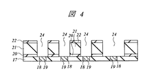
次に、図3に示すように、絶縁膜22上に反射防止膜23aおよびフォトレジスト膜を順に形成し、露光によりフォトレジスト膜をパターン化してフォトレジストパターン23bを形成する。そして、フォトレジストパターン23bをエッチングマスクにしたドライエッチング法により、反射防止膜23aを選択的に除去する。その後、フォトレジストパターン23bをエッチングマスクにしたドライエッチング法により、絶縁膜22を選択的に除去し、開口部を形成する。それから、絶縁膜22の開口部から露出する絶縁膜21をNH3プラズマ処理またはN2/H2プラズマ処理などによってエッチングしながら、フォトレジストパターン23bおよび反射防止膜23aをアッシングして除去する。そして、絶縁膜21および22の開口部から露出する絶縁膜20をドライエッチングによって除去する。これにより、図4に示されように、開口部または配線溝24が形成される。配線溝24の底面からはプラグ19の上面が露出される。なお、フォトレジストパターン23bをエッチングマスクにしたドライエッチング法により、絶縁膜20、21および22を選択的に除去し、開口部または配線溝24を形成した後、フォトレジストパターン23bおよび反射防止膜23aを除去することもできる。
【0037】
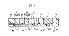
次に、基板1の主面上の全面に、例えば窒化チタン(TiN)などからなる厚さ50nm程度の薄い導電性バリア膜(第1導体膜)25aをスパッタリング法などを用いて形成する。導電性バリア膜25aは、例えば後述の主導体膜形成用の銅の拡散を防止する機能および主導体膜のリフロー時に銅の濡れ性を向上させる機能などを有している。このような導電性バリア膜25aの材料としては、窒化チタンに代えて、銅と殆ど反応しない窒化タングステン(WN)または窒化タンタル(TaN)などのような高融点金属窒化物を用いることもできる。また、導電性バリア膜25aの材料として、高融点金属窒化物にシリコン(Si)を添加した材料や、銅と反応し難いタンタル(Ta)、チタン(Ti)、タングステン(W)、チタンタングステン(TiW)合金などのような高融点金属を用いることもできる。
【0038】
続いて、導電性バリア膜25a上に、例えば厚さ800〜1600nm程度の相対的に厚い銅からなる主導体膜(第2導体膜)25bを形成する。主導体膜25bは、例えばCVD法、スパッタリング法またはめっき法などを用いて形成することができる。その後、例えば475℃程度の非酸化性雰囲気(例えば水素雰囲気)中において基板1に対して熱処理を施すことにより主導体膜25bをリフローさせ、銅を配線溝24の内部に隙間なく埋め込む。
【0039】
次に、主導体膜25b、導電性バリア膜25aおよび絶縁膜22をCMP法によって、絶縁膜21の上面が露出するまで研磨する。これにより、図5に示すように、相対的に薄い導電性バリア膜25aと相対的に厚い主導体膜25bとからなる第2層配線(配線)25を配線溝24内に形成する。第2層配線25は、プラグ19を介して第1層配線15と電気的に接続されている。
【0040】
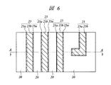
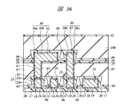
図6は、図5に続く半導体装置の製造工程中における図1に対応する領域の要部平面図を示し、図7は図6のA−A断面図である。なお、図7においても、図2の絶縁膜17より下の構造に対応する部分は図示を省略している。
【0041】
配線溝24内に第2層配線(配線)25を形成した後、半導体基板1をプラズマCVD装置の処理室内に配置し、アンモニアガスを導入してプラズマ電源を印加することにより、基板1(特に第2層配線25が露出するCMP面)に対して、アンモニア(NH3)プラズマ処理を施す。あるいは、N2ガスおよびH2ガスを導入して、N2/H2プラズマ処理を施す。このような還元性プラズマ処理により、CMPで酸化された銅配線表面の酸化銅(CuO、CuO2)を銅(Cu)に還元し、更に、窒化銅(CuN)層が第2層配線25の表面(ごく薄い領域)に形成される。また、このプラズマ処理によって、第2層配線25間の絶縁膜21がエッチングされ除去される。これにより、図6および図7に示される構造が得られる。従って、第2層配線25を形成するために用いられた絶縁膜21は、導電性バリア膜25aおよび銅からなる主導体膜25bに悪影響を与えないような処理、例えば還元性プラズマ処理、によって簡単にエッチングされ得る材料を用いることが好ましい。酸素プラズマ処理によって絶縁膜21を除去する場合は、第2層配線25の上面の銅が酸化されてしまうので、第2層配線25の上面上に導電性バリア膜を選択的に形成しておく必要がある。また、第2層配線25は、その平面形状が、図6に示すように、例えば帯状に形成されている。
【0042】
なお、プラズマ処理とは、プラズマ状態にある環境に、基板表面、あるいは、基板上に絶縁膜、金属膜等のような部材が形成されている時にはその部材表面を暴露し、プラズマの化学的、機械的(ボンバードメント)作用を表面に与えて処理することをいう。また、還元性雰囲気のプラズマとは、還元作用、すなわち、酸素を引き抜く作用を有するラジカル、イオン、原子、分子等の反応種が支配的に存在するプラズマ環境をいう。
【0043】
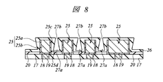
図8は、図7に続く半導体装置の製造工程中における要部断面図を示している。なお、図8においても、図2の絶縁膜17より下の構造に対応する部分は図示を省略している。
【0044】
絶縁膜21が除去された後、洗浄を行い、その後、図8に示すように、半導体基板1の主面の全面上に絶縁膜26をプラズマCVD法などによって形成する。すなわち、第2層配線25の上面および側面を覆うように、絶縁膜26を絶縁膜20上に形成する。絶縁膜26は、例えば窒化シリコン膜からなり、銅配線のバリア絶縁膜として機能する。従って、絶縁膜26は、第2層配線25の主導体膜25b中の銅が、後で形成される層間絶縁膜28中に拡散するのを抑制または防止する。絶縁膜26の他の材料として、例えば炭化シリコン(SiC)膜、炭窒化シリコン(SiCN)膜または酸窒化シリコン(SiON)膜の単体膜を用いても良い。これらの膜を用いた場合、窒化シリコン膜に比べて誘電率を大幅に下げることができるので、配線容量を低減することができ、半導体装置の動作速度を向上させることができる。プラズマCVD法で形成された炭化シリコン膜には、例えばBLOk(AMAT社製)がある。その成膜ガスは、上記した通りである。上記SiCN膜の成膜に際しては、例えばヘリウム(He)と、アンモニア(NH3)と、トリメチルシラン(3MS)との混合ガスを用いる。また、上記プラズマCVD法で形成された酸窒化シリコン膜としては、例えばPE−TMS(Canon製、誘電率=3.9)がある。上記酸窒化シリコン膜の形成に際しては、例えばトリメトキシシラン(TMS)ガスと酸化窒素(N2O)ガスとの混合ガスを用いる。
【0045】
本実施の形態においては、最近接配線間(最小隣接配線間、最小ピッチ配線間)のカバレージがオーバーハングするような条件で、すなわち、最近接配線間では絶縁膜26がコンフォーマルには成膜されない条件で、絶縁膜26を成膜する。ここで、最近接配線とは、同層配線において隣接する配線同士の間隔(隣接配線間距離)が最小である配線に対応する。最近接配線間では、寄生容量の低減がより重要である。
【0046】
隣接配線間では、絶縁膜26の堆積が進行するに従って、対向する配線側面(配線対向面)の上部25c近傍での堆積物に遮られて徐々に反応種が下方に入り込みにくくなる。このため、対向する配線側面の下部25d近傍での堆積速度は上部25c近傍での堆積速度に比べて小さくなる。従って、対向する配線側面上に堆積された絶縁膜26の厚みは、均一にはならず、上部25c近傍での厚みが下部25d近傍よりも厚くなる。このような現象は、第2層配線25の最近接配線間、すなわち第2層配線25のうちの最も近接した配線同士の間では、より顕著である。
【0047】
このため、第2層配線25の最近接配線間では、絶縁膜26は第2層配線25の形状を反映したコンフォーマルな形状にはならず、図8に示されるような溝またはくぼみ部分27aが生じる。絶縁膜26のくぼみ部分27aの上方開口部27bの寸法は、くぼみ部分27aの内部の寸法よりも小さい。すなわち、上方開口部27b近傍において、絶縁膜26のくぼみ部分27aの対向する内壁(絶縁膜26表面)は、上方開口部27bに近づくにつれて徐々に狭まっている。なお、図8においては、くぼみ部分27aの断面形状は、模式的に示されているに過ぎず、くぼみ部分27aは、略楕円形など種々の断面形状を有することができる。また、くぼみ部分27aの上方開口部27bが閉じるまで絶縁膜26の成膜を行ってもよい。また、くぼみ部分27aの上方開口部27bおよび図示しない側方(図8の紙面に垂直な方向)開口部が閉じるまで絶縁膜26の成膜を行い、図9に示されるように、第2層配線25の最近接配線間の絶縁膜26中に絶縁膜26の材料が存在しない空隙またはボイド(void)27cを形成してもよい。従って、本実施の形態では、第2層配線25の最近接配線間を絶縁膜26の材料で完全に満たすことはない。
【0048】
また、絶縁膜26の成膜には、プラズマCVD法などを用いることができ、絶縁膜26の成膜条件を調整することなどにより、上述のようなくぼみ部分27aを最近接配線間に容易に形成することができる。第2層配線25を逆テーパ状に形成する必要はない。このため、第2層配線25の上端部への電界集中を緩和することができる。
【0049】
また、本実施の形態では、第2層配線25の上面および側面をバリア絶縁膜としての絶縁膜26で覆うので、第2層配線25において導電性バリア膜25aを省略し、銅からなる主導体膜25bだけで第2層配線25を形成することもできる。
【0050】
図10〜19は、図8に続く半導体装置の製造工程中における要部断面図を示している。なお、図10〜19においても、図2の絶縁膜17より下の構造に対応する部分は図示を省略している。
【0051】
絶縁膜26を形成した後、絶縁膜28を絶縁膜26上に形成する。本実施の形態では、図10に示すように、絶縁膜28の材料が最近接配線間を完全には埋めないように、すなわちくぼみ部分27aを完全には埋めないように、絶縁膜28を形成する。絶縁膜28は、絶縁膜16と同様の材料、すなわちLow−K材料からなる。上述のように、絶縁膜26のくぼみ部分27aの上方開口部27bの寸法は、くぼみ部分27aの内部の寸法よりも小さい。このため、絶縁膜28を例えば塗布法で形成するとき、第2層配線25の最近接配線間のくぼみ部分27aの内部には絶縁膜28の材料が、その表面張力などのために、ほとんど入り込まない。従って、絶縁膜28が形成された段階で、第2層配線25の最近接配線間には、絶縁膜26および28の材料が存在しない空隙またはボイド27が形成される。ボイド27は絶縁膜26および28の材料によって囲まれた空間であり、その内部は真空であっても、あるいは絶縁膜28の成膜雰囲気の気体成分などが存在していても良い。一方、第2層配線25の隣接配線間距離が大きな領域では、絶縁膜28の材料が第2層配線25間を容易に埋め、ボイド27は形成されない。このため、機械的強度を維持することが可能となる。
【0052】
また、絶縁膜28をCVD法で形成する場合も、第2層配線25の最近接配線間の絶縁膜26のくぼみ部分27aの内部には反応種が入り込みにくい。このため、絶縁膜26のくぼみ部分27a内には絶縁膜28の材料がほとんど堆積されず、第2層配線25の最近接配線間にボイド27が形成される。
【0053】
なお、図10は、図8のように第2層配線25の最近接配線間の絶縁膜26にくぼみ27aが形成されている状態で絶縁膜28を絶縁膜26上に形成した場合について図示している。図9のように第2層配線25の最近接配線間の絶縁膜26中にボイド27cが形成されている場合は、絶縁膜26中のボイド27cに絶縁膜28の材料が侵入することなく、絶縁膜26上に絶縁膜28が形成される。これにより、第2層配線25の最近接配線間に、絶縁膜26および28の材料が存在しない空隙またはボイド27が形成される。
【0054】
また、上層配線(後述する第3層配線38)と下層配線(第2層配線)との間の寄生容量を低減するために、絶縁膜28を上記Low−K材料を用いて形成することが好ましいが、例えばCVD法で形成した酸化シリコン膜などによって絶縁膜28を形成することもできる。ただし、上層配線と下層配線との間の寄生容量を低減するために、絶縁膜28の誘電率は絶縁膜26の誘電率よりも低いことが好ましい。
【0055】
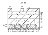
次に、図11に示されるように、絶縁膜28上に絶縁膜29および30をCVD法などを用いて順に形成する。絶縁膜29は、例えば窒化シリコン膜からなり、絶縁膜30は、例えば酸化シリコン膜からなる。必要に応じてCMP処理を行い、絶縁膜30の上面を平坦化する。絶縁膜29の他の材料として、例えば炭化シリコン膜またはSiCN膜を用いても良い。また、絶縁膜30の他の材料として、例えばPE−TMS(Canon製、誘電率=3.9)などの酸窒化シリコン(SiON)膜を用いることができ、場合によっては、絶縁膜30は形成しなくともよい。
【0056】
次に、絶縁膜30上に、絶縁膜31を形成する。絶縁膜31は、絶縁膜21と同様の材料、すなわち還元性プラズマ処理によってエッチングされ得る材料からなることが好ましい。
【0057】
次に、絶縁膜31上に、絶縁膜32および33を順に形成する。絶縁膜32は、絶縁膜22と同様の材料から形成することができる。絶縁膜33は、例えば窒化シリコン膜からなる。また、絶縁膜33の他の材料として、例えば炭化シリコン膜またはSiCN膜を用いても良い。
【0058】
次に、絶縁膜33上に反射防止膜34aおよびフォトレジスト膜を順に形成し、露光によりフォトレジスト膜をパターン化してフォトレジストパターン34bを形成する。これにより、図11に示される構造が得られる。それから、フォトレジストパターン34bをエッチングマスクにしたドライエッチング法により、反射防止膜34aを選択的に除去する。その後、フォトレジストパターン34bをエッチングマスクにしたドライエッチング法により、絶縁膜33を選択的に除去し、開口部35を形成する。開口部35の形成工程では、絶縁膜32をエッチングストッパとして機能させる。
【0059】
次に、残存するフォトレジストパターン34bおよび反射防止膜34aを除去した後、開口部35の内部を含む絶縁膜33上に反射防止膜36aを形成する。そして、反射防止膜36a上にフォトレジスト膜を形成し、露光によりフォトレジスト膜をパターン化してフォトレジストパターン36bを形成する。これにより、図12に示される構造が得られる。
【0060】
次に、フォトレジストパターン36bをエッチングマスクにしたドライエッチング法により、反射防止膜36aを選択的に除去する。それから、フォトレジストパターン36bをエッチングマスクにしたドライエッチング法により、絶縁膜32を選択的に除去して開口部37を形成し、開口部37の底部で絶縁膜31を露出する。そして、開口部37から露出した絶縁膜31をNH3プラズマ処理またはN2/H2プラズマ処理などによってエッチングしながら、フォトレジストパターン36bおよび反射防止膜36aをアッシングして除去する。これにより、図13に示される構造が得られる。フォトレジストパターン36bおよび反射防止膜36aの除去は、絶縁膜31のエッチング工程の後に行うこともできる。
【0061】
次に、図14に示されるように、開口部37の底部で露出する絶縁膜30とその下層の絶縁膜29と、開口部35から露出する絶縁膜32とを、ドライエッチング法などによって除去し、開口部37の底部で絶縁膜28を露出しかつ開口部35から絶縁膜31を露出する。このとき、エッチングマスクとして機能する絶縁膜33は、上部がエッチングされて薄くなるが、絶縁膜33の形成時に比較的厚く形成しておけば、絶縁膜33が完全に除去されることはない。
【0062】
次に、図15に示されるように、開口部37の底部で露出する絶縁膜28と、開口部35から露出する絶縁膜31とを、ドライエッチング法などによって除去する。このとき、絶縁膜33がエッチングマスクとして機能し、かつ絶縁膜26および絶縁膜30がエッチングストッパとして機能する。
【0063】
次に、図16に示されるように、開口部37の底部で露出する絶縁膜26をドライエッチング法などによって除去し、開口部37の底部で第2層配線25を露出させる。このとき、露出した絶縁膜30および絶縁膜33も除去される。
【0064】
次に、基板1の主面上の全面に、導電性バリア膜25aと同様の材料、例えば窒化チタンからなる導電性バリア膜38aをスパッタリング法などで形成する。それから、導電性バリア膜38a上に、開口部37および開口部35を埋めるように、銅からなる主導体膜38bを、主導体膜25bと同様にして形成する。
【0065】
次に、主導体膜38b、導電性バリア膜38aおよび絶縁膜32をCMP法によって、絶縁膜31の上面が露出するまで研磨する。これにより、図17に示されるように、開口部35および37からなる配線溝内に第3層配線(配線)38を形成する。第3層配線38は、相対的に薄い導電性バリア膜38aと、相対的に厚い主導体膜38bとを有しており、第2層配線25と電気的に接続されている。
【0066】
次に、第2層配線25間の絶縁膜21を除去するプラズマ処理と同様の処理を施し、第3層配線38間の絶縁膜31を除去する。それから、第3層配線38のバリア絶縁膜としての絶縁膜39を、絶縁膜26と同様にして形成する。これにより、図18に示されるように、くぼみ部分27aと同様のくぼみ部分40aが、第3層配線38の最近接配線間に生じる。
【0067】
次に、図19に示されるように、絶縁膜39上に、絶縁膜28と同様のLow−K材料からなる絶縁膜41を形成する。絶縁膜28の形成工程と同様、第3層配線38の最近接配線間の絶縁膜39のくぼみ部分40aの内部には絶縁膜41の材料が、その表面張力などのために入り込めない。このため、絶縁膜41を形成した段階で、第3層配線38の最近接配線間には空隙またはボイド40が形成される。一方、第3層配線38の隣接配線間距離が大きな領域では、絶縁膜41の材料が第2層配線38間に入り込み、ボイドが形成されないので、機械的強度を維持することが可能となる。
【0068】
次に、絶縁膜41上に絶縁膜42をCVD法などを用いて形成する。絶縁膜41は、例えば窒化シリコン膜からなる。必要に応じてCMP処理を行い、絶縁膜41の上面を平坦化する。絶縁膜41の他の材料として、例えば炭化シリコン膜、SiCN膜または酸窒化シリコン膜を用いることもできる。これより、図19に示される構造が得られる。更に必要に応じて、同様の製造工程を繰り返し、第4層配線以降の上層配線を形成することもできる。また、第1層配線15を、第2層配線25と同様にして形成した銅配線とし、第2層配線25を第3層配線38と同様にして形成した銅配線とすることもできる。
【0069】
本実施の形態によれば、同層配線間にCMP面(CMPで研磨された面)がない。すなわち、第2層配線25および第3層配線38を形成するためのCMP工程で研磨された絶縁膜21および31は除去されており、第2層配線25および第3層配線38を覆うようにバリア絶縁膜26および39が形成されている。このため、第2層配線25および第3層配線38において、同層配線の上面同士がCMP面を介して連結されることはない。これにより、TDDB寿命を向上し、配線間の絶縁破壊耐性を向上させることができる。また、半導体装置の信頼性を高めることができる。
【0070】
また、最も容量低減が必要な同層配線における最近接配線間に膜材料が存在しないボイド27および40を形成するので、配線間容量を低減することができる。配線のバリア絶縁膜26および39に比較的誘電率の高い材料を用いたとしても、配線間容量の低減が可能である。
【0071】
また、同層配線の隣接配線間距離が大きな領域では、配線間にボイドを形成せずLow−K材料を成膜する。このため、全体の機械的強度を維持することが可能となる。
【0072】
また、本実施の形態では、最近接配線間でなくとも、隣接配線間隔が比較的小さく、その間の寄生容量を低減したい配線間にはボイド27または40を形成してもよい。配線間距離がどの程度の場合までボイドを形成するかは、絶縁膜26または39の成膜条件や絶縁膜28または41の成膜条件などを調整することによって、制御することができる。これにより、配線パターン密度が疎の領域では、隣接配線間にボイドを形成して配線間容量を低減し、配線パターンが密な領域では、配線間をLow−K材料で埋めて、機械的強度を確保することができる。
【0073】
本発明者は、実験およびシミュレーションにより、本実施の形態の配線構造の容量低減効果について調べた。比較例として、配線を埋め込むための絶縁膜および層間絶縁膜をLow−K材料で構成しかつ一般的なダマシン技術で形成された銅配線構造を用いた。
【0074】
その結果、本実施の形態の配線構造は、上記比較例に対して、配線間容量を20〜30%程度低減することができた。また、上層配線と下層配線の間の容量はほとんど変わらず、同層の配線間容量のみが減少した。このため、配線のクロストークの影響を低減できる。また、実効誘電率εr(上記比較例の銅配線構造ではεrは3.1程度)を2.3〜2.7程度へ大幅に低減することができた。従って、同世代のLow−K材料を層間絶縁膜に用いて、1世代以上先の低容量配線構造を実現できる。
【0075】
(実施の形態2)
図20〜25は、本発明の他の実施の形態である半導体装置の製造工程中の要部断面図である。図10までの製造工程は上記実施の形態1と同様であるので、ここではその説明は省略し、図10に続く製造工程について説明する。
【0076】
図10に示される構造が形成された後、図20に示されるように、絶縁膜28上に、例えば窒化シリコン膜からなる絶縁膜29と例えば酸化シリコン膜からなる絶縁膜30とをCVD法などを用いて順に形成する。必要に応じてCMP処理を行い、絶縁膜30の上面を平坦化する。場合によっては、絶縁膜30は形成しなくともよい。
【0077】
次に、絶縁膜33上に反射防止膜50aおよびフォトレジスト膜を順に形成し、露光によりフォトレジスト膜をパターン化してフォトレジストパターン50bを形成する。
【0078】
次に、図21に示されるように、フォトレジストパターン50bをエッチングマスクにしたドライエッチング法により、反射防止膜50aを選択的に除去した後、フォトレジストパターン50bをエッチングマスクにしたドライエッチング法により、絶縁膜29および30を選択的に除去し、開口部51を形成する。開口部51の形成工程では、絶縁膜28をエッチングストッパとして機能させる。その後、残存するフォトレジストパターン50bおよび反射防止膜50aを除去する。
【0079】
次に、開口部51内を含む絶縁膜30上に、絶縁膜31を形成する。それから、絶縁膜31上に、絶縁膜32を形成する。上記実施の形態1とは異なり、本実施の形態では、絶縁膜33は形成しなくともよい。
【0080】
次に、絶縁膜32上に反射防止膜52aを形成する。そして、反射防止膜52a上にフォトレジスト膜を形成し、露光によりフォトレジスト膜をパターン化してフォトレジストパターン52bを形成する。これにより、図22に示される構造が得られる。
【0081】
次に、フォトレジストパターン52bをエッチングマスクにしたドライエッチング法により、反射防止膜52aを選択的に除去する。それから、フォトレジストパターン52bをエッチングマスクにしたドライエッチング法により、絶縁膜32を選択的に除去して開口部53を形成し、開口部53の底部で絶縁膜31を露出する。その後、NH3プラズマ処理またはN2/H2プラズマ処理などによって、開口部53から露出した絶縁膜31と開口部51から露出する絶縁膜28とをエッチングしながら、フォトレジストパターン52bおよび反射防止膜52aをアッシングして除去する。このとき、かつ絶縁膜26および絶縁膜30がエッチングストッパとして機能する。これにより、図23に示される構造が得られる。フォトレジストパターン52bおよび反射防止膜52aの除去は、絶縁膜28および31のエッチング工程の後に行うこともできる。
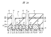
【0082】
次に、図24に示されるように、開口部51の底部で露出する絶縁膜26をドライエッチング法などによって除去し、開口部51の底部で第2層配線25を露出させる。このとき、露出した絶縁膜30および絶縁膜32も除去され得る。
【0083】
次に、基板1の主面上の全面に、例えば窒化チタンからなる導電性バリア膜38aをスパッタリング法などで形成する。それから、導電性バリア膜38a上に、開口部51および開口部53を埋めるように、銅からなる主導体膜38bを形成する。
【0084】
次に、主導体膜38bおよび導電性バリア膜38aをCMP法によって、絶縁膜31の上面が露出するまで研磨する。これにより、図25に示されるように、開口部51および53からなる配線溝内に第3層配線(配線)38を形成する。第3層配線38は、相対的に薄い導電性バリア膜38aと、相対的に厚い主導体膜38bとを有しており、第2層配線25と電気的に接続されている。
【0085】
これ以降の製造工程は、上記実施の形態1の図17以降の製造工程と同様であるので、その説明を省略する。
【0086】
(実施の形態3)
図26は、本発明の他の実施の形態である半導体装置の製造工程中の要部断面図である。本実施の形態の半導体装置は、上記実施の形態1の第2層配線25および第3層配線36ように隣接配線間にボイドを形成しかつ隣接配線間をCMP面で接続しない配線層と、一般的な埋込配線技術を用いて形成された配線層とが組み合わされた多層配線構造を有している。図26において、絶縁膜42の形成工程までは、上記実施の形態1の図19までの製造工程とほぼ同様であるので、その説明は省略し、ここではそれ以降の製造工程について説明する。
【0087】
本実施の形態では、絶縁膜42上に酸化シリコンなどからなる絶縁膜60が形成され、第3層配線38と同様にして第4層配線61が形成される。それから、絶縁膜26と同様にして、バリア絶縁膜として機能する絶縁膜62が形成され、その上に絶縁膜28と同様にして絶縁膜64を形成する。第4層配線61においても、第2層配線25および第3層配線36と同様、最近接配線間にボイド63が形成される。
【0088】
第5層以降の配線層は、一般的な埋込配線技術、例えば一般的なデュアルダマシン技術を用いて形成する。すなわち、絶縁膜64上に、窒化シリコン、炭化シリコン、炭窒化シリコンまたは酸窒化シリコン膜(例えばPE−TMS(Canon製))からなる絶縁膜65、酸化シリコンなどからなる絶縁膜66、Low−K材料などからなる絶縁膜67、絶縁膜65と同様の材料、例えば窒化シリコンなどからなる絶縁膜68および酸化シリコンなどからなる絶縁膜69を形成する。そして、デュアルダマシン技術を用いて、絶縁膜62、64〜69に形成された配線溝に埋め込まれた第5層配線70を形成する。それから、第5層配線70の上面を含む絶縁膜69上に、窒化シリコン、炭化シリコン、炭窒化シリコンまたは酸窒化シリコン膜などからなる絶縁膜71を、バリア絶縁膜として形成する。その後、絶縁膜71上に、Low−K材料などからなる絶縁膜72、絶縁膜65と同様の材料、例えば窒化シリコンなどからなる絶縁膜73、酸化シリコンなどからなる絶縁膜74、Low−K材料などからなる絶縁膜75、絶縁膜65と同様の材料、例えば窒化シリコンなどからなる絶縁膜76および酸化シリコンなどからなる絶縁膜77を形成する。そして、デュアルダマシン技術を用いて、絶縁膜71〜77に形成された配線溝に埋め込まれた第6層配線78を形成する。それから、第6層配線78の上面を含む絶縁膜77上に、絶縁膜71と同様の材料、例えば窒化シリコンなどからなる絶縁膜79を、バリア絶縁膜として形成する。
【0089】
なお、絶縁膜28、41、64、67、72および75としてCVD法を用いて形成した膜、例えば酸化シリコン膜、FSG(SiOF系材料)膜、SiOC膜またはポーラスシリコン(Polus−Si)系材料膜を用いることもでき、その場合、絶縁膜30、60、66、68、69、74、76および77の形成を省略することもできる。
【0090】
多層配線構造において、隣接配線間隔が比較的小さい、すなわち配線ピッチが比較的小さい配線層では、配線間容量が増大しかつTDDB寿命が低減しやすい。本実施の形態によれば、そのような配線間容量が増大しかつTDDB寿命が低減しやすい配線層において、同層配線間にCMP面をなくしてTDDB寿命を向上させ、かつ同層配線の最近接配線間にボイドを形成して配線間容量を低減することができる。
【0091】
(実施の形態4)
図27、29〜31は、本発明の他の実施の形態である半導体装置の配線パターンを示す概念的な平面図である。図28は図27のB−B断面図である。配線パターンの構造および形成工程は上記実施の形態1の第2層配線25または第3層配線36とほぼ同様であるので、ここではその説明は省略する。
【0092】
本実施の形態においては、本体配線81の周囲に、ダミー配線82を設ける。本体配線81は、半導体装置の電気回路として必要不可欠な配線パターンである。本体配線81は、例えば上記第2層配線25または第3層配線38などに対応し、MISFETのゲートやソース・ドレイン領域などに電気的に接続されている。ダミー配線82は、本体配線81と同時に形成されかつ同構造の導体パターンであるが、半導体装置の電気回路としては必要とされない、すなわち配線としては機能しない導体パターンである。ダミー配線82は、例えば、MISFETのゲートやソース・ドレイン領域などに電気的に接続されることなく、接地電位とされている。本実施の形態においては、隣接する本体配線81間にボイド(図示せず)を形成するとともに、本体配線81とダミー配線82の間にもボイド(図示せず)を形成する。ボイドの形成工程は、上記実施の形態1と同様である。ダミー配線82を設けたことにより、本体配線81の両側にボイドを形成することができる。このため、本体配線81の寄生容量をより低減することが可能になる。図27〜30は、本体配線81とダミー配線82の形成パターンの例を示しており、必要に応じて、図27〜30およびそれ以外の種々の配線パターンを形成することができる。
【0093】
例えば、図27および図28に示されるように、孤立した一本の本体配線81を囲むようにダミー配線82を設けることができる。
【0094】
また、図29に示されるように、互いに平行に配列する複数の本体配線81の全体を囲むようにダミー配線82を設けることができる。
【0095】
また、図30に示されるように、互いに平行に配列する複数の本体配線81全体を囲むようにダミー配線82を設けるとともに、複数の本体配線81間にもダミー配線82を設けることができる。
【0096】
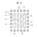
また、ダミー配線82パターンは連続して形成しなくともよく、例えば図31に示されるように、不連続なダミー配線82を設けることもできる。
【0097】
(実施の形態5)
図32は、本発明の他の実施の形態である半導体装置の配線パターンを示す概念的な平面図である。図32の配線パターン85は、例えば上記第2層配線25または第3層配線36に対応し、その構造および形成工程は上記実施の形態1と同様であるので、ここではその説明は省略する。
【0098】
本実施の形態では、配線パターン85において、スルーホール形成領域86の近傍で、配線幅広部またはリザーバ部87を設けている。これにより、スルーホールが配線パターンからずれる、目外れを防止する。図32では、その上に形成すべきスルーホールに対応する位置86を点線で示してある。スルーホール形成のためのフォトリソグラフィ工程において、フォトマスクの位置ずれなどにより、実際に形成されたスルーホールの位置が所望の位置(図32の点線の位置)からずれる場合がある。このような場合でも、配線幅が広いリザーバ部87が設けられているので、スルーホールが配線パターン85から外れることを防止できる。このため、配線85に隣接して形成されるボイド(図示せず)が、スルーホールの形成工程で露出することをより的確に防止できる。
【0099】
(実施の形態6)
図33は、本発明の他の実施の形態である半導体装置の製造工程中の要部断面図であり、図19の工程段階に対応する。
【0100】
本実施の形態では、上記実施の形態1とは異なり、銅配線のバリア絶縁膜として機能する絶縁膜26および39を形成しない。本実施の形態では、銅配線である第2層配線25および第3層配線38の上部に、銅の拡散を防止する導電性バリア膜として、例えばタングステンなどからなる金属キャップ膜91および92を形成する。従って、第2層配線25は、導電性バリア膜25a、主導体膜25bおよび金属キャップ膜91から構成され、第3層配線38は、導電性バリア膜38a、主導体膜38bおよび金属キャップ膜92から構成される。また、絶縁膜26および39を形成しないので、Low−K材料からなる絶縁膜28および39が第2層配線25および第3層配線36の同層隣接配線間を完全に埋め、最近接配線間においてもボイド27および40は形成されない。
【0101】
金属キャップ膜91は、選択タングステンCVD法などによって形成することができる。例えば、図5に示すように配線溝に埋め込まれた第2層配線25を形成した後、六フッ化タングステン(WF6)および水素(H2)ガスを用いたCVD法により、絶縁膜21から露出した第2層配線25の上面上にタングステン膜を選択的に堆積することにより、金属キャップ膜91を形成する。その後、絶縁膜21を除去し、バリア絶縁膜26を形成することなく、第2層配線25を覆いかつ隣接配線間を埋めるように、絶縁膜28を形成する。金属キャップ膜92も金属キャップ膜91と同様にして形成することができる。金属キャップ膜91および92の他の材料としては、バリア膜として機能する他の高融点金属または高融点金属窒化物、例えば窒化チタン(TiN)または窒化タンタル(TaN)などを用いることができる。他の構造および製造工程は、上記実施の形態1とほぼ同様であるので、ここでは詳しい説明を省略する。
【0102】
本実施の形態によれば、銅配線としての第2層配線25および第3層配線38において、銅からなる主導体膜25bおよび38bの底面および側面を窒化チタンなどからなる導電性バリア膜25aおよび38aで覆い、かつ主導体膜25bおよび38bの上面をタングステンなどからなる金属キャップ膜91および92で覆う。このため、第2層配線25および第3層配線38に対してバリア絶縁膜を形成する必要がない。同層配線間にCMP面がないのでTDDB寿命を向上し、配線間の絶縁破壊耐性を向上させることができる。これにより、半導体装置の信頼性を高めることができる。また、同層隣接配線間をLow−K材料膜だけで埋めることができるので、配線間容量を低減することが可能となる。
【0103】
(実施の形態7)
図34は、本発明の他の実施の形態である半導体装置の製造工程中の要部断面図であり、図19の工程段階に対応する。
【0104】
本実施の形態では、上記実施の形態1とは異なり、銅配線のバリア絶縁膜として機能する絶縁膜26および39は、第2層配線25および第3層配線38に対してコンフォーマルに形成されている。すなわち、絶縁膜26および39は、第2層配線25および第3層配線38の形状を反映した形状を有し、それぞれいずれの領域においてもほぼ均一な厚みを有している。このため、絶縁膜26のくぼみ部分27dの間口部の寸法は、くぼみ部分27dの内部の寸法とほぼ同じである。従って、絶縁膜28は、絶縁膜28を構成するLow−K材料が絶縁膜26のくぼみ部分27dを埋めるように形成される。すなわち、第2層配線25の最近接配線間においても、ボイドは形成されず、Low−K材料が埋め込まれる。第3層配線38についても同様である。他の構造および製造工程は、上記実施の形態1と同様であるので、ここでは詳しい説明を省略する。
【0105】
本実施の形態によれば、同層配線間にCMP面がないのでTDDB寿命を向上し、配線間の絶縁破壊耐性を向上させることができる。これにより、半導体装置の信頼性を高めることができる。また、同層隣接配線間をバリア絶縁膜とLow−K材料膜だけで埋めるので、配線間容量を低減することができる。
【0106】
(実施の形態8)
図35は、本発明の他の実施の形態である半導体装置の製造工程中の要部断面図であり、図19の工程段階に対応する。
【0107】
本実施の形態では、上記実施の形態6と同様に、銅配線のバリア絶縁膜として機能する絶縁膜26および39は形成せず、第2層配線25および第3層配線38の上部に、銅の拡散を防止する導電性バリア膜として、例えばタングステンなどからなる金属キャップ膜91および92を形成する。従って、第2層配線25は、導電性バリア膜25a、主導体膜25bおよび金属キャップ膜91から構成され、第3層配線38は、導電性バリア膜38a、主導体膜38bおよび金属キャップ膜92から構成される。
【0108】
しかしながら、本実施の形態では、上記実施の形態6とは異なり、第2層配線25および第3層配線36の同層隣接配線間、例えば最近接配線間に、ボイド93および94が形成される。ボイド93は、例えば次のようにして形成することができる。第2層配線25を覆うように絶縁膜20上に絶縁膜28を形成する際に、上記実施の形態1の絶縁膜26の形成工程のように、最近接配線間のカバレージがオーバーハングするような条件で絶縁膜28を成膜する。絶縁膜28は所定の膜厚になるまで成膜される。これにより、最近接配線間の絶縁膜28中にボイド93が形成される。ボイド94も、ボイド93と同様にして形成することができる。従って、本実施の形態では、絶縁膜28および41は、CVD法で形成され得るLow−K材料からなることが好ましく、例えば、CVD法で形成されたFSG(SiOF系材料)膜、SiOC膜またはポーラスシリコン(Polus−Si)系材料膜を用いることができる。また、CVD法を用いて形成した酸化シリコン膜を用いることも可能である。他の構造および製造工程は、上記実施の形態1とほぼ同様であるので、ここでは詳しい説明を省略する。
【0109】
本実施の形態によれば、銅配線としての第2層配線25および第3層配線38において、銅からなる主導体膜25bおよび38bの底面および側面を窒化チタンなどからなる導電性バリア膜25aおよび38aで覆い、かつ主導体膜25bおよび38bの上面をタングステンなどからなる金属キャップ膜91および92で覆う。このため、第2層配線25および第3層配線38に対してバリア絶縁膜を形成する必要がない。同層配線間にCMP面がないのでTDDB寿命を向上し、配線間の絶縁破壊耐性を向上させることができる。これにより、半導体装置の信頼性を高めることができる。また、最も容量低減が必要な同層配線における最近接配線間にボイドを形成し、ボイド以外の領域はLow−K材料膜だけで埋めることもできる。これにより、配線間容量を低減することが可能である。
【0110】
(実施の形態9)
図36は、本発明の他の実施の形態である半導体装置の製造工程中の要部断面図であり、図19の工程段階に対応する。
【0111】
本実施の形態では、上記実施の形態6および8と同様に、銅配線のバリア絶縁膜として機能する絶縁膜26および39は形成せず、第2層配線25および第3層配線38の上部に、銅の拡散を防止する導電性バリア膜として、例えばタングステンなどからなる金属キャップ膜91および92を形成する。従って、第2層配線25は、導電性バリア膜25a、主導体膜25bおよび金属キャップ膜91から構成され、第3層配線38は、導電性バリア膜38a、主導体膜38bおよび金属キャップ膜92から構成される。
【0112】
しかしながら、本実施の形態では、上記実施の形態6とは異なり、第2層配線25および第3層配線36の同層隣接配線間、例えば最近接配線間に、ボイド96および99が形成される。ボイド96は、例えば次のようにして形成することができる。
【0113】
第2層配線25を覆うように絶縁膜20上に絶縁膜95をCVD法などによって形成する。絶縁膜95は、CVD法で形成され得るLow−K材料からなることが好ましく、例えば、CVD法で形成されたFSG(SiOF系材料)膜、SiOC膜またはポーラスシリコン(Polus−Si)系材料膜を用いることができる。CVD法を用いて形成した酸化シリコン膜を用いることも可能である。この際、上記実施の形態1の絶縁膜26の形成工程のように、最近接配線間のカバレージがオーバーハングするような条件で絶縁膜95を成膜する。これにより、第2層配線25の最近接配線間の絶縁膜95に、上記実施の形態1のくぼみ部分27aと同様のくぼみ部分が形成される。それから、絶縁膜95上に絶縁膜97を、塗布法などによって形成する。絶縁膜97は、塗布法によって形成され得るLow−K材料からなることが好ましいが、塗布法以外の方法によって形成されるLow−K材料を用いることもできる。上記実施の形態1の絶縁膜28の形成工程と同様、第2層配線25の最近接配線間の絶縁膜95のくぼみ部分に絶縁膜97の材料が、その表面張力などのためにほとんど入り込まない。このため、本実施の形態においては、上記実施の形態1と同様、第2層配線25の最近接配線間に、絶縁膜95および97によって囲まれたボイド96が形成される。
【0114】
ボイド99も、ボイド96と同様にして形成することができる。すなわち、絶縁膜95と同様の材料からなる絶縁膜98と、絶縁膜97と同様の材料からなる絶縁膜100とが順に形成されて、第3層配線36の最近接配線間に、絶縁膜98および100によって囲まれたボイド99が形成される。他の構造および製造工程は、上記実施の形態1とほぼ同様であるので、ここでは詳しい説明を省略する。
【0115】
本実施の形態によれば、銅配線としての第2層配線25および第3層配線38において、銅からなる主導体膜25bおよび38bの底面および側面を窒化チタンなどからなる導電性バリア膜25aおよび38aで覆い、かつ主導体膜25bおよび38bの上面をタングステンなどからなる金属キャップ膜91および92で覆う。このため、第2層配線25および第3層配線38に対してバリア絶縁膜を形成する必要がない。同層配線間にCMP面がないのでTDDB寿命を向上し、配線間の絶縁破壊耐性を向上させることができる。これにより、半導体装置の信頼性を高めることができる。また、最も容量低減が必要な同層配線における最近接配線間にボイドを形成し、ボイド以外の領域はLow−K材料膜だけで埋めることもできる。これにより、配線間容量を低減することが可能である。
【0116】
以上、本発明者によってなされた発明をその実施の形態に基づき具体的に説明したが、本発明は前記実施の形態に限定されるものではなく、その要旨を逸脱しない範囲で種々変更可能であることは言うまでもない。
【0117】
前記実施の形態では、CMISFETを有する半導体装置について説明したが、本発明は、これに限定されるものではなく、銅を主成分とする主導体膜を含む配線を有する種々の半導体装置に適用することができる。
【0118】
【発明の効果】
本願において開示される発明のうち、代表的なものによって得られる効果を簡単に説明すれば以下のとおりである。
【0119】
銅を主導体層とする配線間の絶縁破壊耐性を向上することができる。
【0120】
銅を主導体層とする配線間の容量を低減することができる。
【図面の簡単な説明】
【図1】本発明の一実施の形態である半導体装置の製造工程中の要部平面図である。
【図2】図1のA−A線の断面図である。
【図3】図2に続く半導体装置の製造工程中における要部断面図である。
【図4】図3に続く半導体装置の製造工程中における要部断面図である。
【図5】図4に続く半導体装置の製造工程中における要部断面図である。
【図6】図5に続く半導体装置の製造工程中における要部平面図である。
【図7】図6のA−A線の断面図である。
【図8】図7に続く半導体装置の製造工程中における要部断面図である。
【図9】図7に続く半導体装置の製造工程中における要部断面図である。
【図10】図8に続く半導体装置の製造工程中における要部断面図である。
【図11】図10に続く半導体装置の製造工程中における要部断面図である。
【図12】図11に続く半導体装置の製造工程中における要部断面図である。
【図13】図12に続く半導体装置の製造工程中における要部断面図である。
【図14】図13に続く半導体装置の製造工程中における要部断面図である。
【図15】図14に続く半導体装置の製造工程中における要部断面図である。
【図16】図15に続く半導体装置の製造工程中における要部断面図である。
【図17】図16に続く半導体装置の製造工程中における要部断面図である。
【図18】図17に続く半導体装置の製造工程中における要部断面図である。
【図19】図18に続く半導体装置の製造工程中における要部断面図である。
【図20】本発明の他の実施の形態である半導体装置の製造工程中の要部断面図である。
【図21】図20に続く半導体装置の製造工程中における要部断面図である。
【図22】図21に続く半導体装置の製造工程中における要部断面図である。
【図23】図22に続く半導体装置の製造工程中における要部断面図である。
【図24】図23に続く半導体装置の製造工程中における要部断面図である。
【図25】図24に続く半導体装置の製造工程中における要部断面図である。
【図26】本発明の他の実施の形態である半導体装置の製造工程中の要部断面図である。
【図27】本発明の他の実施の形態である半導体装置の配線パターンを示す平面図である。
【図28】図27のB−B線の断面図である。
【図29】本発明の他の実施の形態である半導体装置の配線パターンを示す平面図である。
【図30】本発明の他の実施の形態である半導体装置の配線パターンを示す平面図である。
【図31】本発明の他の実施の形態である半導体装置の配線パターンを示す平面図である。
【図32】本発明の他の実施の形態である半導体装置の配線パターンを示す平面図である。
【図33】本発明の他の実施の形態である半導体装置の製造工程中の要部断面図である。
【図34】本発明の他の実施の形態である半導体装置の製造工程中の要部断面図である。
【図35】本発明の他の実施の形態である半導体装置の製造工程中の要部断面図である。
【図36】本発明の他の実施の形態である半導体装置の製造工程中の要部断面図である。
【符号の説明】
1 半導体基板
2 素子分離領域
3 p型ウエル
4 n型ウエル
5 nチャネル型MISFET
6 pチャネル型MISFET
7 ゲート絶縁膜
8 ゲート電極
9 サイドウォール
10a n-型半導体領域
10b n+型半導体領域
11a p-型半導体領域
11b p+型半導体領域
12 絶縁膜
13 コンタクトホール
14 プラグ
14a 窒化チタン膜
15 第1層配線
16,17 絶縁膜
18 スルーホール
19 プラグ
20〜22 絶縁膜
23a 反射防止膜
23b フォトレジストパターン
24 配線溝
25 第2層配線
25a 導電性バリア膜
25b 主導体膜
26 絶縁膜
27 ボイド
27a くぼみ部分
27b 開口部
27c ボイド
28〜33 絶縁膜
34a 反射防止膜
34b フォトレジストパターン
35 開口部
36a 反射防止膜
36b フォトレジストパターン
37 開口部
38 第3層配線
38a 導電性バリア膜
38b 主導体膜
39 絶縁膜
40 ボイド
40a くぼみ部分
41,42 絶縁膜
50a 反射防止膜
50b フォトレジストパターン
51 開口部
52a 反射防止膜
52b フォトレジストパターン
53 開口部
60 絶縁膜
61 第4層配線
62 絶縁膜
63 ボイド
64〜69 絶縁膜
70 第5層配線
71〜77 絶縁膜
78 第6層配線
79 絶縁膜
81 本体配線
82 ダミー配線
85 配線パターン
86 スルーホール形成位置
87 リザーバ部
91,92 金属キャップ膜
93,94 ボイド
95 絶縁膜
96 ボイド
97 絶縁膜
98 絶縁膜
99 ボイド
100 絶縁膜[0001]
BACKGROUND OF THE INVENTION
The present invention relates to a semiconductor device and a manufacturing technique thereof, and more particularly, to a technology effective when applied to a semiconductor device having a wiring including a main conductor film containing copper as a main component.
[0002]
[Prior art]
The embedded wiring structure has Damascene technology (Single-Damascene technology and Dual-Damascene technology) in wiring openings such as wiring trenches and holes formed in insulating films. It is formed by embedding a wiring material by a so-called wiring forming technique. However, when the main wiring material is copper (Cu), copper is more easily diffused into the insulating film than a metal such as aluminum (Al), so the embedded wiring made of copper is directly connected to the insulating film. By covering the surface (bottom surface and side surface) of the embedded wiring with a thin barrier metal film so as not to contact, copper in the embedded wiring is suppressed or prevented from diffusing into the insulating film. Further, by forming a wiring cap barrier insulating film made of, for example, a silicon nitride film on the upper surface of the insulating film in which the wiring opening is formed, and covering the upper surface of the embedded wiring, the copper in the embedded wiring is The diffusion from the upper surface of the buried wiring into the insulating film is suppressed or prevented.
[0003]
In recent years, the interval between such embedded wirings has been reduced as semiconductor devices are highly integrated. As a result, the parasitic capacitance between the wirings increases, causing a signal delay, and crosstalk occurs between adjacent wirings. For this reason, it is desired to reduce the parasitic capacitance between the wirings. In order to reduce the parasitic capacitance between the wirings, a low dielectric constant material is used as the insulating film between the wirings. For example, Japanese Patent Application Laid-Open No. 2001-85519 discloses a technique in which wirings are formed in a reverse taper shape, and an interlayer insulating film is formed so that an air gap is formed in a space between the wirings. By this air gap, the wiring capacitance is reduced.
[0004]
[Problems to be solved by the invention]
However, according to the examination results of the present inventors, it has been found that the embedded wiring technology using the copper as the main conductor layer has the following problems.
[0005]
When copper is used as a wiring material, there is a problem that a TDDB (Time Dependence on Dielectric Breakdown) life is significantly shorter than other metal materials (for example, aluminum and tungsten). Furthermore, in addition to the trend toward finer wiring pitches and increased effective electric field strength, in recent years, insulating materials having a dielectric constant lower than that of silicon oxide have been used as insulating films between wirings in order to reduce wiring capacitance. However, since an insulating film having a low dielectric constant generally has a low withstand voltage, it is increasingly difficult to ensure the TDDB life.
[0006]
The deterioration of the TDDB life is generally considered that copper applied to the wiring material diffuses to the periphery, which reduces the dielectric breakdown voltage between the wirings. In the above Japanese Patent Laid-Open No. 2001-85519, no consideration is given to the barrier metal film and the barrier insulating film. For this reason, even if the inter-wiring capacitance is reduced due to the air gap of the interlayer insulating film, copper used as the wiring material diffuses into the interlayer insulating film and the TDDB life is reduced. Further, since the air gap is formed by giving the wiring an inverse taper, the electric field concentrates on the upper end portion of the wiring, and the TDDB life is further reduced.
[0007]
An object of the present invention is to provide a semiconductor device capable of improving the dielectric breakdown resistance between wirings using copper as a main conductor layer, and a manufacturing method thereof.
[0008]
Another object of the present invention is to provide a semiconductor device capable of reducing the capacitance between wirings having copper as a main conductor layer, and a method for manufacturing the same.
[0009]
The above and other objects and novel features of the present invention will be apparent from the description of this specification and the accompanying drawings.
[0010]
[Means for Solving the Problems]
Of the inventions disclosed in the present application, the outline of typical ones will be briefly described as follows.
[0011]
The semiconductor device of the present invention includes a semiconductor substrate, a first insulating film formed on the semiconductor substrate, a wiring formed on the first insulating film and containing copper as a main component, a top surface and a side surface of the wiring, and a first A second insulating film formed on the insulating film and having a function of suppressing or preventing copper diffusion; and a third insulating film formed on the second insulating film and having a dielectric constant lower than that of the second insulating film. The insulating film is provided.
[0012]
The method for manufacturing a semiconductor device of the present invention includes a step of preparing a semiconductor substrate, a step of forming a first insulating film on the semiconductor substrate, a step of forming a wiring containing copper as a main component on the first insulating film, Forming a second insulating film having a function of suppressing or preventing copper diffusion on the upper and side surfaces of the wiring and the first insulating film so as not to fill between the wirings with the material; The method includes a step of forming a third insulating film having a dielectric constant lower than that of the film on the second insulating film.
[0013]
DETAILED DESCRIPTION OF THE INVENTION
Hereinafter, embodiments of the present invention will be described in detail with reference to the drawings. Note that components having the same function are denoted by the same reference symbols throughout the drawings for describing the embodiments, and the repetitive description thereof will be omitted. In the following embodiments, the description of the same or similar parts will not be repeated in principle unless particularly necessary.
[0014]
(Embodiment 1)
First, the cause of deterioration of the TDDB life between the embedded wirings using the above copper as the main conductor layer studied by the present inventors will be described. The TDDB (Time Dependence on Dielectric Breakdown) lifetime is a measure for objectively measuring the time dependency of dielectric breakdown, and is relatively high between electrodes under a predetermined temperature (eg, 140 ° C.) measurement condition. Create a graph in which the time from voltage application to dielectric breakdown is plotted against the applied electric field by applying voltage, and the time (lifetime) obtained by extrapolating from this graph to the actual electric field strength (for example, 0.2 MV / cm) ).
[0015]
The deterioration of the TDDB life is generally considered that copper applied to the wiring material diffuses to the periphery, which reduces the dielectric breakdown voltage between the wirings. However, according to the examination results by the present inventors, the following factors are dominant in the copper diffusion phenomenon. That is, first, in copper diffused in the insulating film between adjacent wirings, ionized copper supplied from copper oxide (CuO) or copper silicide drifts and diffuses at the potential between the wirings rather than atomic copper. The factor is dominant. Second, the copper diffusion path is dominated by the interface between the insulating film on which the copper wiring is formed and the wiring cap film. From these facts, it was found that the deterioration of the TDDB life is due to the following mechanism.
[0016]
That is, copper oxide (CuO) is formed on the surface of the embedded wiring using copper as a main conductor film by a surface process after CMP, and copper silicide (CuN) is formed when a cap film (silicon nitride film) is formed. Compound). Such copper oxide or copper silicide is easily ionized as compared with pure copper. The copper ionized in this way is drifted by the electric field between the wirings and diffused into the insulating film between the wirings. On the other hand, the interface between the insulating film (silicon oxide film) and the cap film (silicon nitride film) forming the embedded wiring is discontinuous due to the formation of a lot of CMP damage, organic matter or dangling bonds. poor. The presence of such dangling bonds has an effect of promoting the diffusion of the copper ions, and the copper ions are drifted and diffused along the interface. That is, a leak path is formed at the interface between the wirings. The leakage current flowing through the leakage path is also subjected to a long-term leakage action and thermal stress due to the current, and then the current value increases at an accelerated rate, leading to dielectric breakdown (decrease in TDDB life). The cause of the deterioration of the TDDB life is disclosed in Japanese Patent Application No. 11-226876, Japanese Patent Application No. 2000-104015, or Japanese Patent Application No. 2000-300853 by the inventors of the present application.
[0017]
Therefore, in the present embodiment, it has been studied to improve the TDDB characteristics by eliminating the CMP surface (surface polished by CMP) which is the interface acting as the leak path from between the same-layer wirings. Furthermore, reduction of the parasitic capacitance between wirings was also examined.
[0018]
The semiconductor device of this embodiment and its manufacturing process will be described with reference to the drawings. FIG. 1 is a plan view of an essential part during a manufacturing process of a semiconductor device according to an embodiment of the present invention, for example, a CMISFET (Complementary Metal Insulator Semiconductor Field Effect Transistor), and FIG. 2 is a cross-sectional view taken along line AA in FIG. FIG.
[0019]
As shown in FIGS. 1 and 2, a wafer or semiconductor substrate 1 made of p-type single crystal silicon having a specific resistance of about 1 to 10 Ωcm, for example, has an
[0020]
A p-
[0021]
In the region of the p-
[0022]
The
[0023]
The source and drain regions of the n-type MISFET 5 are n -
[0024]
The source and drain regions of the p-type MISFET 6 are p - Type semiconductor region 11a and p having a higher impurity concentration + And an LDD structure having a type semiconductor region 11b. p - The type semiconductor region 11a is formed, for example, by ion-implanting impurities such as boron into regions on both sides of the
[0025]
An insulating
[0026]
A
[0027]
On the insulating
[0028]
An insulating
[0029]
Examples of the organic polymer as the low dielectric constant material include SiLK (manufactured by The Dow Chemical Co., USA, relative dielectric constant = 2.7, heat resistant temperature = 490 ° C. or higher, dielectric breakdown voltage = 4.0 to 5.0 MV / Vm). ) Or FLARE of polyallyl ether (PAE) material (manufactured by Honeywell Electronic Materials, relative permittivity = 2.8, heat-resistant temperature = 400 ° C. or higher). This PAE material is characterized by high basic performance and excellent mechanical strength, thermal stability and low cost. Examples of the organic silica glass (SiOC-based material) as the low dielectric constant material include, for example, HSG-R7 (manufactured by Hitachi Chemical Co., Ltd., relative dielectric constant = 2.8, heat resistant temperature = 650 ° C.), Black Diamond (Applied Materials, USA) Inc., relative dielectric constant = 3.0 to 2.4, heat-resistant temperature = 450 ° C.) or p-MTES (manufactured by Hitachi Development Co., Ltd., relative dielectric constant = 3.2). Other SiOC materials include, for example, CORAL (manufactured by Novellus Systems, Inc., relative permittivity = 2.7 to 2.4, heat-resistant temperature = 500 ° C.), Aurora 2.7 (manufactured by Japan ASM Co., Ltd.) , Relative dielectric constant = 2.7, heat-resistant temperature = 450 ° C.).
[0030]
Examples of the low dielectric constant material of the insulating
[0031]
An insulating
[0032]
3 to 5 are fragmentary cross-sectional views of the semiconductor device during the manufacturing process subsequent to FIG. For easy understanding, in FIGS. 3 to 5, the portions corresponding to the structure below the insulating
[0033]
First, in the present embodiment, as shown in FIG. 3, the insulating
[0034]
Next, an insulating
[0035]
Next, the insulating
[0036]
Next, as shown in FIG. 3, an
[0037]
Next, a thin conductive barrier film (first conductor film) 25a made of titanium nitride (TiN) or the like and having a thickness of about 50 nm is formed on the entire main surface of the substrate 1 using a sputtering method or the like. The
[0038]
Subsequently, a main conductor film (second conductor film) 25b made of relatively thick copper having a thickness of, for example, about 800 to 1600 nm is formed on the
[0039]
Next, the
[0040]
6 is a plan view of a principal part of a region corresponding to FIG. 1 in the manufacturing process of the semiconductor device subsequent to FIG. 5, and FIG. 7 is a cross-sectional view taken along line AA of FIG. Also in FIG. 7, the illustration corresponding to the structure below the insulating
[0041]
After the second-layer wiring (wiring) 25 is formed in the
[0042]
The plasma treatment means that the surface of the substrate or the surface of the member such as an insulating film or a metal film is formed on the substrate in an environment in a plasma state, and the chemical surface of the plasma is exposed. It means that the surface is treated with mechanical (bombardment) action. In addition, the plasma in a reducing atmosphere refers to a plasma environment in which reactive species such as radicals, ions, atoms, and molecules that have a reducing action, that is, an action of extracting oxygen, exist predominantly.
[0043]
FIG. 8 is a fragmentary cross-sectional view of the semiconductor device during a manufacturing step following that of FIG. 7. In FIG. 8 as well, portions corresponding to the structure below the insulating
[0044]
After the insulating
[0045]
In the present embodiment, the insulating
[0046]
As the deposition of the insulating
[0047]
For this reason, the insulating
[0048]
Further, the insulating
[0049]
In the present embodiment, since the upper surface and the side surface of the
[0050]
10 to 19 are fragmentary cross-sectional views of the semiconductor device during the manufacturing process subsequent to FIG. 10 to 19, the portions corresponding to the structure below the insulating
[0051]
After forming the insulating
[0052]
Further, when the insulating
[0053]
10 illustrates the case where the insulating
[0054]
In order to reduce the parasitic capacitance between the upper layer wiring (
[0055]
Next, as shown in FIG. 11, insulating
[0056]
Next, an insulating
[0057]
Next, insulating
[0058]
Next, an
[0059]
Next, after removing the remaining
[0060]
Next, the
[0061]
Next, as shown in FIG. 14, the insulating
[0062]
Next, as shown in FIG. 15, the insulating
[0063]
Next, as shown in FIG. 16, the insulating
[0064]
Next, a
[0065]
Next, the
[0066]
Next, processing similar to the plasma processing for removing the insulating
[0067]
Next, as shown in FIG. 19, an insulating
[0068]
Next, the insulating
[0069]
According to this embodiment, there is no CMP surface (surface polished by CMP) between the same-layer wirings. That is, the insulating
[0070]
Further, since the
[0071]
In a region where the distance between adjacent wirings of the same layer wiring is large, a Low-K material is formed without forming a void between the wirings. For this reason, it becomes possible to maintain the whole mechanical strength.
[0072]
Further, in this embodiment, even if not between the nearest wirings, the interval between adjacent wirings is relatively small, and voids 27 or 40 may be formed between the wirings for which the parasitic capacitance between them is to be reduced. To what extent the inter-wiring distance is formed can be controlled by adjusting the film formation conditions of the insulating
[0073]
The inventor investigated the capacitance reduction effect of the wiring structure of the present embodiment through experiments and simulations. As a comparative example, a copper wiring structure in which an insulating film and an interlayer insulating film for embedding the wiring are made of a Low-K material and is formed by a general damascene technique is used.
[0074]
As a result, the wiring structure of the present embodiment was able to reduce the inter-wiring capacitance by about 20 to 30% compared to the comparative example. In addition, the capacitance between the upper layer wiring and the lower layer wiring hardly changed, and only the capacitance between the wirings in the same layer decreased. For this reason, the influence of the crosstalk of wiring can be reduced. Further, the effective dielectric constant εr (εr is about 3.1 in the copper wiring structure of the comparative example) can be greatly reduced to about 2.3 to 2.7. Therefore, a low-capacity wiring structure of one generation or more can be realized by using the same generation Low-K material for the interlayer insulating film.
[0075]
(Embodiment 2)
20 to 25 are fragmentary cross-sectional views of the semiconductor device according to another embodiment of the present invention during the manufacturing process. Since the manufacturing process up to FIG. 10 is the same as that of the first embodiment, the description thereof is omitted here, and the manufacturing process following FIG. 10 will be described.
[0076]
After the structure shown in FIG. 10 is formed, as shown in FIG. 20, an insulating
[0077]
Next, an
[0078]
Next, as shown in FIG. 21, after the
[0079]
Next, the insulating
[0080]
Next, an
[0081]
Next, the
[0082]
Next, as shown in FIG. 24, the insulating
[0083]
Next, a
[0084]
Next, the
[0085]
Since the subsequent manufacturing steps are the same as the manufacturing steps in FIG. 17 and subsequent drawings of the first embodiment, description thereof will be omitted.
[0086]
(Embodiment 3)
FIG. 26 is a fragmentary sectional view in the process of manufacturing a semiconductor device according to another embodiment of the present invention. The semiconductor device of the present embodiment includes a wiring layer in which voids are formed between adjacent wirings and the adjacent wirings are not connected on the CMP surface as in the
[0087]
In the present embodiment, the insulating
[0088]
The fifth and subsequent wiring layers are formed using a general buried wiring technique, for example, a general dual damascene technique. That is, the insulating
[0089]
The insulating
[0090]
In a multilayer wiring structure, a wiring layer having a relatively small interval between adjacent wirings, that is, a wiring layer having a relatively small wiring pitch, tends to increase the inter-wiring capacity and reduce the TDDB life. According to the present embodiment, in such a wiring layer in which the capacitance between wirings is increased and the TDDB life is likely to be reduced, the CMP surface is eliminated between the wirings in the same layer to improve the TDDB life. By forming voids between the contact wires, the capacitance between wires can be reduced.
[0091]
(Embodiment 4)
27 and 29 to 31 are conceptual plan views showing wiring patterns of a semiconductor device according to another embodiment of the present invention. 28 is a cross-sectional view taken along the line BB in FIG. Since the structure of the wiring pattern and the formation process are substantially the same as those of the
[0092]
In the present embodiment, a
[0093]
For example, as shown in FIGS. 27 and 28, a
[0094]
Further, as shown in FIG. 29, dummy wirings 82 can be provided so as to surround the whole of the plurality of main body wirings 81 arranged in parallel to each other.
[0095]
Further, as shown in FIG. 30, dummy wirings 82 can be provided so as to surround the plurality of main body wirings 81 arranged in parallel to each other, and dummy wirings 82 can be provided between the plurality of
[0096]
Further, the
[0097]
(Embodiment 5)
FIG. 32 is a conceptual plan view showing a wiring pattern of a semiconductor device according to another embodiment of the present invention. The
[0098]
In the present embodiment, in the
[0099]
(Embodiment 6)
FIG. 33 is a fragmentary cross-sectional view of the semiconductor device according to another embodiment of the present invention during the manufacturing process, corresponding to the process step of FIG.
[0100]
In the present embodiment, unlike the first embodiment, the insulating
[0101]
The
[0102]
According to the present embodiment, in the
[0103]
(Embodiment 7)
FIG. 34 is a fragmentary cross-sectional view of the semiconductor device according to another embodiment of the present invention during the manufacturing process, corresponding to the process step of FIG.
[0104]
In the present embodiment, unlike the first embodiment, the insulating
[0105]
According to the present embodiment, since there is no CMP surface between the same-layer wirings, the TDDB life can be improved and the dielectric breakdown resistance between the wirings can be improved. Thereby, the reliability of the semiconductor device can be improved. Further, since the space between adjacent wirings in the same layer is filled with only the barrier insulating film and the Low-K material film, the capacitance between the wirings can be reduced.
[0106]
(Embodiment 8)
FIG. 35 is a fragmentary cross-sectional view of the semiconductor device according to another embodiment of the present invention during the manufacturing process, corresponding to the process step of FIG.
[0107]
In the present embodiment, as in the sixth embodiment, the insulating
[0108]
However, in the present embodiment, unlike the sixth embodiment, voids 93 and 94 are formed between adjacent wirings of the
[0109]
According to the present embodiment, in the
[0110]
(Embodiment 9)
FIG. 36 is a fragmentary cross-sectional view of the semiconductor device according to another embodiment of the present invention during the manufacturing process, corresponding to the process step of FIG.
[0111]
In the present embodiment, as in the sixth and eighth embodiments, the insulating
[0112]
However, in the present embodiment, unlike the sixth embodiment, voids 96 and 99 are formed between adjacent wirings in the same layer of the
[0113]
An insulating
[0114]
The void 99 can be formed in the same manner as the
[0115]
According to the present embodiment, in the
[0116]
As mentioned above, the invention made by the present inventor has been specifically described based on the embodiment. However, the invention is not limited to the embodiment, and various modifications can be made without departing from the scope of the invention. Needless to say.
[0117]
In the above embodiment, the semiconductor device having the CMISFET has been described. However, the present invention is not limited to this, and the present invention is applied to various semiconductor devices having wirings including a main conductor film containing copper as a main component. be able to.
[0118]
【The invention's effect】
Among the inventions disclosed in the present application, effects obtained by typical ones will be briefly described as follows.
[0119]
It is possible to improve dielectric breakdown resistance between wirings using copper as a main conductor layer.
[0120]
It is possible to reduce the capacitance between wirings using copper as the main conductor layer.
[Brief description of the drawings]
FIG. 1 is a fragmentary plan view of a semiconductor device in an embodiment of the invention during a manufacturing process;
FIG. 2 is a cross-sectional view taken along line AA in FIG.
3 is a fragmentary cross-sectional view of the semiconductor device during a manufacturing step following that of FIG. 2; FIG.
4 is a fragmentary cross-sectional view of the semiconductor device during a manufacturing step following that of FIG. 3; FIG.
5 is a fragmentary cross-sectional view of the semiconductor device during a manufacturing step following that of FIG. 4; FIG.
6 is a substantial part plan view of the semiconductor device in manufacturing process subsequent to FIG. 5; FIG.
7 is a cross-sectional view taken along line AA in FIG.
8 is a fragmentary cross-sectional view of the semiconductor device during a manufacturing step following that of FIG. 7; FIG.
9 is a fragmentary cross-sectional view of the semiconductor device during a manufacturing step following that of FIG. 7; FIG.
10 is a fragmentary cross-sectional view of the semiconductor device during a manufacturing step following that of FIG. 8; FIG.
11 is a fragmentary cross-sectional view of the semiconductor device during a manufacturing step following that of FIG. 10; FIG.
12 is a fragmentary cross-sectional view of the semiconductor device during a manufacturing step following that of FIG. 11; FIG.
13 is a fragmentary cross-sectional view of the semiconductor device during a manufacturing step following that of FIG. 12; FIG.
14 is a fragmentary cross-sectional view of the semiconductor device during a manufacturing step following that of FIG. 13; FIG.
15 is a fragmentary cross-sectional view of the semiconductor device during a manufacturing step following that of FIG. 14; FIG.
16 is a fragmentary cross-sectional view of the semiconductor device during a manufacturing step following that of FIG. 15; FIG.
FIG. 17 is a fragmentary cross-sectional view of the semiconductor device during a manufacturing step following that of FIG. 16;
FIG. 18 is a fragmentary cross-sectional view of the semiconductor device during a manufacturing step following that of FIG. 17;
FIG. 19 is a fragmentary cross-sectional view of the semiconductor device during a manufacturing step following that of FIG. 18;
FIG. 20 is a fragmentary cross-sectional view of the semiconductor device according to another embodiment of the present invention during the manufacturing steps thereof;
FIG. 21 is a fragmentary cross-sectional view of the semiconductor device during the manufacturing step following that of FIG. 20;
22 is a fragmentary cross-sectional view of the semiconductor device during the manufacturing step following that of FIG. 21; FIG.
FIG. 23 is a fragmentary cross-sectional view of the semiconductor device during a manufacturing step following that of FIG. 22;
24 is a fragmentary cross-sectional view of the semiconductor device during the manufacturing step following that of FIG. 23; FIG.
25 is a fragmentary cross-sectional view of the semiconductor device during the manufacturing step following that of FIG. 24; FIG.
FIG. 26 is a fragmentary cross-sectional view of the semiconductor device according to another embodiment of the present invention during the manufacturing steps thereof;
FIG. 27 is a plan view showing a wiring pattern of a semiconductor device according to another embodiment of the present invention;
28 is a sectional view taken along line BB in FIG. 27. FIG.
FIG. 29 is a plan view showing a wiring pattern of a semiconductor device according to another embodiment of the present invention;
30 is a plan view showing a wiring pattern of a semiconductor device according to another embodiment of the present invention; FIG.
FIG. 31 is a plan view showing a wiring pattern of a semiconductor device according to another embodiment of the present invention;
FIG. 32 is a plan view showing a wiring pattern of a semiconductor device according to another embodiment of the present invention;
33 is a cross-sectional view of essential parts in the process of manufacturing a semiconductor device according to another embodiment of the present invention. FIG.
FIG. 34 is a fragmentary cross-sectional view of the semiconductor device as another embodiment of the present invention during the manufacturing steps thereof;
35 is a cross-sectional view of essential parts in the process of manufacturing a semiconductor device according to another embodiment of the present invention. FIG.
FIG. 36 is a fragmentary cross-sectional view of the semiconductor device according to another embodiment of the present invention during the manufacturing steps thereof;
[Explanation of symbols]
1 Semiconductor substrate
2 Device isolation region
3 p-type well
4 n-type well
5 n-channel MISFET
6 p-channel MISFET
7 Gate insulation film
8 Gate electrode
9 Sidewall
10a n - Type semiconductor region
10b n + Type semiconductor region
11a p - Type semiconductor region
11b p + Type semiconductor region
12 Insulating film
13 Contact hole
14 plug
14a Titanium nitride film
15 First layer wiring
16, 17 Insulating film
18 Through hole
19 plug
20-22 Insulating film
23a Antireflection film
23b Photoresist pattern
24 Wiring groove
25 Second layer wiring
25a Conductive barrier film
25b Main conductor film
26 Insulating film
27 void
27a Recessed part
27b opening
27c void
28-33 Insulating film
34a Antireflection film
34b Photoresist pattern
35 opening
36a Antireflection film
36b Photoresist pattern
37 opening
38 Third layer wiring
38a Conductive barrier film
38b Main conductor film
39 Insulating film
40 void
40a Recessed part
41, 42 Insulating film
50a Antireflection film
50b photoresist pattern
51 opening
52a Antireflection film
52b Photoresist pattern
53 opening
60 Insulating film
61 4th layer wiring
62 Insulating film
63 void
64-69 Insulating film
70 5th layer wiring
71-77 Insulating film
78 6th layer wiring
79 Insulating film
81 Body wiring
82 Dummy wiring
85 Wiring pattern
86 Through-hole formation position
87 Reservoir part
91,92 Metal cap film
93, 94 void
95 Insulating film
96 void
97 Insulating film
98 Insulating film
99 void
100 Insulating film
Claims (6)
(b)前記半導体基板上に第1の絶縁膜を形成する工程、
(c)前記第1の絶縁膜上に銅を主成分として含む配線を形成する工程、
(d)銅の拡散を抑制または防止する機能を有する第2の絶縁膜を、その材料で前記配線の少なくとも一部の隣接配線間が満たされないように、前記配線の上面および側面上と前記第1の絶縁膜上とに形成する工程、および、
(e)前記第2の絶縁膜の誘電率より低い誘電率を有する第3の絶縁膜を、前記第2の絶縁膜上に形成する工程、
を有し、
ここで、前記(c)工程は、
前記第1の絶縁膜上に第4の絶縁膜を形成する工程、
前記第4の絶縁膜に開口部を形成する工程、
前記第4の絶縁膜の前記開口部内に、銅を主成分として含む配線を形成する工程、および、
前記第4の絶縁膜を除去する工程、
を有し、
ここで、前記第4の絶縁膜は、還元性プラズマ処理によりエッチングされ得る材料を含み、
前記第4の絶縁膜を除去する工程では、還元性プラズマ処理により前記第4の絶縁膜が除去されることを特徴とする半導体装置の製造方法。 (A) a step of preparing a semiconductor substrate;
(B) forming a first insulating film on the semiconductor substrate;
(C) forming a wiring containing copper as a main component on the first insulating film;
(D) The second insulating film having a function of suppressing or preventing copper diffusion is formed on the upper and side surfaces of the wiring and the second insulating film so that at least part of the adjacent wiring of the wiring is not filled with the material. Forming on one insulating film; and
(E) a third insulating film having a lower dielectric constant than the second insulating film, forming on said second insulating film,
Have
Here, the step (c)
Forming a fourth insulating film on the first insulating film;
Forming an opening in the fourth insulating film;
Forming a wiring containing copper as a main component in the opening of the fourth insulating film; and
Removing the fourth insulating film;
Have
Here, the fourth insulating film includes a material that can be etched by reducing plasma treatment,
In the step of removing the fourth insulating film, the fourth insulating film is removed by reducing plasma treatment.
前記(e)工程では、前記配線の隣接配線間に前記第2の絶縁膜と前記第3の絶縁膜とで囲まれたボイドが形成されることを特徴とする半導体装置の製造方法。In the manufacturing method of the semiconductor device according to claim 1 ,
In the step (e), a void surrounded by the second insulating film and the third insulating film is formed between adjacent wirings of the wiring.
前記(e)工程では、前記配線の最近接配線間に前記第2の絶縁膜と前記第3の絶縁膜とで囲まれたボイドが形成されることを特徴とする半導体装置の製造方法。In the manufacturing method of the semiconductor device according to claim 1 ,
In the step (e), a void surrounded by the second insulating film and the third insulating film is formed between the closest wirings of the wiring.
前記(d)工程では、前記配線の隣接配線間を埋める前記第2の絶縁膜で囲まれたボイドが形成されることを特徴とする半導体装置の製造方法。In the manufacturing method of the semiconductor device according to claim 1 ,
In the step (d), a void surrounded by the second insulating film that fills between adjacent wirings of the wiring is formed.
前記(d)工程では、前記配線の隣接配線間において、対向する配線側面の上方での前記第2の絶縁膜の堆積速度が下方での堆積速度より大きくなるように前記第2の絶縁膜が形成されることを特徴とする半導体装置の製造方法。The method of manufacturing a semiconductor device according to claim 2 .
In the step (d), between the adjacent wirings of the wiring, the second insulating film is formed so that the deposition rate of the second insulating film above the opposing wiring side surface is larger than the deposition rate below. A method of manufacturing a semiconductor device, comprising: forming a semiconductor device.
前記(e)工程では、前記第2の絶縁膜で覆われた前記配線の隣接配線間が前記第3の絶縁膜で満たされないことによって、前記隣接配線間に前記第2の絶縁膜と前記第3の絶縁膜とで囲まれたボイドが形成されることを特徴とする半導体装置の製造方法。In the manufacturing method of the semiconductor device according to claim 1 ,
In the step (e), a gap between the adjacent wirings of the wiring covered with the second insulating film is not filled with the third insulating film, so that the second insulating film and the first wiring are interposed between the adjacent wirings. 3. A method of manufacturing a semiconductor device, wherein a void surrounded by three insulating films is formed.
Priority Applications (4)
| Application Number | Priority Date | Filing Date | Title |
|---|---|---|---|
| JP2002094351A JP4068868B2 (en) | 2002-03-29 | 2002-03-29 | Manufacturing method of semiconductor device |
| US10/387,504 US7042095B2 (en) | 2002-03-29 | 2003-03-14 | Semiconductor device including an interconnect having copper as a main component |
| TW092106945A TW200404353A (en) | 2002-03-29 | 2003-03-27 | A semiconductor device and a method of manufacturing the same |
| KR10-2003-0019462A KR20030078750A (en) | 2002-03-29 | 2003-03-28 | Semiconductor device and method of manufacturing the same |
Applications Claiming Priority (1)
| Application Number | Priority Date | Filing Date | Title |
|---|---|---|---|
| JP2002094351A JP4068868B2 (en) | 2002-03-29 | 2002-03-29 | Manufacturing method of semiconductor device |
Publications (3)
| Publication Number | Publication Date |
|---|---|
| JP2003297918A JP2003297918A (en) | 2003-10-17 |
| JP2003297918A5 JP2003297918A5 (en) | 2005-04-14 |
| JP4068868B2 true JP4068868B2 (en) | 2008-03-26 |
Family
ID=28449690
Family Applications (1)
| Application Number | Title | Priority Date | Filing Date |
|---|---|---|---|
| JP2002094351A Expired - Fee Related JP4068868B2 (en) | 2002-03-29 | 2002-03-29 | Manufacturing method of semiconductor device |
Country Status (1)
| Country | Link |
|---|---|
| JP (1) | JP4068868B2 (en) |
Families Citing this family (16)
| Publication number | Priority date | Publication date | Assignee | Title |
|---|---|---|---|---|
| CN100352036C (en) | 2002-10-17 | 2007-11-28 | 株式会社瑞萨科技 | Semiconductor device and method for manufacturing the same |
| JP4454242B2 (en) | 2003-03-25 | 2010-04-21 | 株式会社ルネサステクノロジ | Semiconductor device and manufacturing method thereof |
| JP4619705B2 (en) * | 2004-01-15 | 2011-01-26 | 株式会社東芝 | Semiconductor device |
| JP2005217371A (en) * | 2004-02-02 | 2005-08-11 | Matsushita Electric Ind Co Ltd | Semiconductor device and method of manufacturing the same |
| JP4401874B2 (en) | 2004-06-21 | 2010-01-20 | 株式会社ルネサステクノロジ | Semiconductor device |
| JP4956919B2 (en) | 2005-06-08 | 2012-06-20 | 株式会社日立製作所 | Semiconductor device and manufacturing method thereof |
| JP4334589B2 (en) | 2006-12-06 | 2009-09-30 | 株式会社東芝 | Semiconductor device and manufacturing method thereof |
| JP5334434B2 (en) * | 2007-06-04 | 2013-11-06 | パナソニック株式会社 | Manufacturing method of semiconductor device |
| US7879683B2 (en) * | 2007-10-09 | 2011-02-01 | Applied Materials, Inc. | Methods and apparatus of creating airgap in dielectric layers for the reduction of RC delay |
| JP5097501B2 (en) * | 2007-10-18 | 2012-12-12 | 株式会社日立製作所 | Manufacturing method of semiconductor integrated circuit device |
| CN101419933B (en) * | 2007-10-24 | 2010-12-15 | 中芯国际集成电路制造(上海)有限公司 | Protection layer making method capable of avoiding projection generation |
| JP4675393B2 (en) * | 2008-05-12 | 2011-04-20 | パナソニック株式会社 | Semiconductor device and manufacturing method of semiconductor device |
| JP5396065B2 (en) | 2008-10-28 | 2014-01-22 | 株式会社日立製作所 | Manufacturing method of semiconductor device |
| KR20120030782A (en) | 2010-09-20 | 2012-03-29 | 삼성전자주식회사 | Method of forming through silicon via using low-k material |
| JP5932079B2 (en) * | 2015-02-26 | 2016-06-08 | ルネサスエレクトロニクス株式会社 | Semiconductor device |
| KR102606765B1 (en) * | 2018-02-07 | 2023-11-27 | 삼성전자주식회사 | Seniconductor device including via plug and method of forming the same |
-
2002
- 2002-03-29 JP JP2002094351A patent/JP4068868B2/en not_active Expired - Fee Related
Also Published As
| Publication number | Publication date |
|---|---|
| JP2003297918A (en) | 2003-10-17 |
Similar Documents
| Publication | Publication Date | Title |
|---|---|---|
| JP4956919B2 (en) | Semiconductor device and manufacturing method thereof | |
| US7042095B2 (en) | Semiconductor device including an interconnect having copper as a main component | |
| US10304726B2 (en) | Semiconductor device and manufacturing method thereof | |
| JP5396065B2 (en) | Manufacturing method of semiconductor device | |
| JP4173374B2 (en) | Manufacturing method of semiconductor device | |
| US20060183317A1 (en) | Semiconductor device and a method of manufacturing the same | |
| JP4068868B2 (en) | Manufacturing method of semiconductor device | |
| JP2004193431A (en) | Semiconductor device and its manufacturing method | |
| KR100860133B1 (en) | Locally increasing sidewall density by ion implantation | |
| JP2005136152A (en) | Method for manufacturing semiconductor device | |
| JP5326949B2 (en) | Semiconductor device | |
| JP2012080133A (en) | Manufacturing method of semiconductor device | |
| JP2003332340A (en) | Manufacturing method of semiconductor device | |
| JP2004111795A (en) | Method of manufacturing semiconductor device |
Legal Events
| Date | Code | Title | Description |
|---|---|---|---|
| A621 | Written request for application examination |
Free format text: JAPANESE INTERMEDIATE CODE: A621 Effective date: 20040329 |
|
| A521 | Request for written amendment filed |
Free format text: JAPANESE INTERMEDIATE CODE: A523 Effective date: 20040329 |
|
| A521 | Request for written amendment filed |
Free format text: JAPANESE INTERMEDIATE CODE: A523 Effective date: 20040604 |
|
| A977 | Report on retrieval |
Free format text: JAPANESE INTERMEDIATE CODE: A971007 Effective date: 20050120 |
|
| A131 | Notification of reasons for refusal |
Free format text: JAPANESE INTERMEDIATE CODE: A131 Effective date: 20070925 |
|
| A521 | Request for written amendment filed |
Free format text: JAPANESE INTERMEDIATE CODE: A523 Effective date: 20071126 |
|
| TRDD | Decision of grant or rejection written | ||
| A01 | Written decision to grant a patent or to grant a registration (utility model) |
Free format text: JAPANESE INTERMEDIATE CODE: A01 Effective date: 20071218 |
|
| A61 | First payment of annual fees (during grant procedure) |
Free format text: JAPANESE INTERMEDIATE CODE: A61 Effective date: 20080111 |
|
| FPAY | Renewal fee payment (event date is renewal date of database) |
Free format text: PAYMENT UNTIL: 20110118 Year of fee payment: 3 |
|
| R150 | Certificate of patent or registration of utility model |
Free format text: JAPANESE INTERMEDIATE CODE: R150 Ref document number: 4068868 Country of ref document: JP Free format text: JAPANESE INTERMEDIATE CODE: R150 |
|
| FPAY | Renewal fee payment (event date is renewal date of database) |
Free format text: PAYMENT UNTIL: 20110118 Year of fee payment: 3 |
|
| S111 | Request for change of ownership or part of ownership |
Free format text: JAPANESE INTERMEDIATE CODE: R313111 |
|
| FPAY | Renewal fee payment (event date is renewal date of database) |
Free format text: PAYMENT UNTIL: 20110118 Year of fee payment: 3 |
|
| R350 | Written notification of registration of transfer |
Free format text: JAPANESE INTERMEDIATE CODE: R350 |
|
| FPAY | Renewal fee payment (event date is renewal date of database) |
Free format text: PAYMENT UNTIL: 20110118 Year of fee payment: 3 |
|
| FPAY | Renewal fee payment (event date is renewal date of database) |
Free format text: PAYMENT UNTIL: 20120118 Year of fee payment: 4 |
|
| FPAY | Renewal fee payment (event date is renewal date of database) |
Free format text: PAYMENT UNTIL: 20130118 Year of fee payment: 5 |
|
| FPAY | Renewal fee payment (event date is renewal date of database) |
Free format text: PAYMENT UNTIL: 20130118 Year of fee payment: 5 |
|
| FPAY | Renewal fee payment (event date is renewal date of database) |
Free format text: PAYMENT UNTIL: 20140118 Year of fee payment: 6 |
|
| R250 | Receipt of annual fees |
Free format text: JAPANESE INTERMEDIATE CODE: R250 |
|
| S111 | Request for change of ownership or part of ownership |
Free format text: JAPANESE INTERMEDIATE CODE: R313113 |
|
| R350 | Written notification of registration of transfer |
Free format text: JAPANESE INTERMEDIATE CODE: R350 |
|
| R250 | Receipt of annual fees |
Free format text: JAPANESE INTERMEDIATE CODE: R250 |
|
| R250 | Receipt of annual fees |
Free format text: JAPANESE INTERMEDIATE CODE: R250 |
|
| R250 | Receipt of annual fees |
Free format text: JAPANESE INTERMEDIATE CODE: R250 |
|
| R250 | Receipt of annual fees |
Free format text: JAPANESE INTERMEDIATE CODE: R250 |
|
| R250 | Receipt of annual fees |
Free format text: JAPANESE INTERMEDIATE CODE: R250 |
|
| R250 | Receipt of annual fees |
Free format text: JAPANESE INTERMEDIATE CODE: R250 |
|
| R250 | Receipt of annual fees |
Free format text: JAPANESE INTERMEDIATE CODE: R250 |
|
| R250 | Receipt of annual fees |
Free format text: JAPANESE INTERMEDIATE CODE: R250 |
|
| LAPS | Cancellation because of no payment of annual fees |