JP4068559B2 - Field probe - Google Patents
Field probe Download PDFInfo
- Publication number
- JP4068559B2 JP4068559B2 JP2003533377A JP2003533377A JP4068559B2 JP 4068559 B2 JP4068559 B2 JP 4068559B2 JP 2003533377 A JP2003533377 A JP 2003533377A JP 2003533377 A JP2003533377 A JP 2003533377A JP 4068559 B2 JP4068559 B2 JP 4068559B2
- Authority
- JP
- Japan
- Prior art keywords
- dipole
- resistors
- conductors
- diodes
- field probe
- Prior art date
- Legal status (The legal status is an assumption and is not a legal conclusion. Google has not performed a legal analysis and makes no representation as to the accuracy of the status listed.)
- Expired - Fee Related
Links
Images


Classifications
-
- G—PHYSICS
- G01—MEASURING; TESTING
- G01R—MEASURING ELECTRIC VARIABLES; MEASURING MAGNETIC VARIABLES
- G01R29/00—Arrangements for measuring or indicating electric quantities not covered by groups G01R19/00 - G01R27/00
- G01R29/08—Measuring electromagnetic field characteristics
- G01R29/0864—Measuring electromagnetic field characteristics characterised by constructional or functional features
- G01R29/0878—Sensors; antennas; probes; detectors
-
- H—ELECTRICITY
- H01—ELECTRIC ELEMENTS
- H01Q—ANTENNAS, i.e. RADIO AERIALS
- H01Q1/00—Details of, or arrangements associated with, antennas
- H01Q1/36—Structural form of radiating elements, e.g. cone, spiral, umbrella; Particular materials used therewith
- H01Q1/38—Structural form of radiating elements, e.g. cone, spiral, umbrella; Particular materials used therewith formed by a conductive layer on an insulating support
-
- H—ELECTRICITY
- H01—ELECTRIC ELEMENTS
- H01Q—ANTENNAS, i.e. RADIO AERIALS
- H01Q1/00—Details of, or arrangements associated with, antennas
- H01Q1/12—Supports; Mounting means
- H01Q1/22—Supports; Mounting means by structural association with other equipment or articles
- H01Q1/24—Supports; Mounting means by structural association with other equipment or articles with receiving set
- H01Q1/248—Supports; Mounting means by structural association with other equipment or articles with receiving set provided with an AC/DC converting device, e.g. rectennas
-
- H—ELECTRICITY
- H01—ELECTRIC ELEMENTS
- H01Q—ANTENNAS, i.e. RADIO AERIALS
- H01Q21/00—Antenna arrays or systems
- H01Q21/06—Arrays of individually energised antenna units similarly polarised and spaced apart
- H01Q21/20—Arrays of individually energised antenna units similarly polarised and spaced apart the units being spaced along or adjacent to a curvilinear path
-
- H—ELECTRICITY
- H01—ELECTRIC ELEMENTS
- H01Q—ANTENNAS, i.e. RADIO AERIALS
- H01Q21/00—Antenna arrays or systems
- H01Q21/29—Combinations of different interacting antenna units for giving a desired directional characteristic
-
- H—ELECTRICITY
- H01—ELECTRIC ELEMENTS
- H01Q—ANTENNAS, i.e. RADIO AERIALS
- H01Q23/00—Antennas with active circuits or circuit elements integrated within them or attached to them
-
- H—ELECTRICITY
- H01—ELECTRIC ELEMENTS
- H01Q—ANTENNAS, i.e. RADIO AERIALS
- H01Q9/00—Electrically-short antennas having dimensions not more than twice the operating wavelength and consisting of conductive active radiating elements
- H01Q9/04—Resonant antennas
- H01Q9/16—Resonant antennas with feed intermediate between the extremities of the antenna, e.g. centre-fed dipole
Abstract
Description
本発明は、全体として、無線アンテナに関し、特に、フィールド・プローブ(field probe)として知られる特殊な形態のアンテナの改良に関する。フィールド・プローブは、無線周波数電磁界の強度を計るために使われる。フィールド・プローブは、特に、試験下の電子装置が特定の周波数帯の強い電磁界に曝される電磁感受性(electromagnetic susceptibility)試験機を較正するのに役立つ。本発明は、特に、E−フィールド・プローブ(E-field probe)の改良に関する。 The present invention relates generally to wireless antennas, and more particularly to improvements in a special form of antenna known as a field probe. Field probes are used to measure the strength of radio frequency electromagnetic fields. Field probes are particularly useful for calibrating electromagnetic susceptibility testing machines in which the electronic device under test is exposed to a strong electromagnetic field in a particular frequency band. The present invention particularly relates to improvements in E-field probes.
電磁感受性試験用E−フィールド・プローブは、全体として、処理回路を有するハウジングに取付けられた1つ以上のショートアンテナを有する。給電ケーブルがあることにより生じるアンテナパターンの歪みを最小化するために、処理回路は、典型的には、検波された高周波電圧を変調光線に変換する変換器を有し、その変調光線はプローブから光ファイバケーブルを通って伝わる。光ファイバケーブルは、レーザ光線の形で、処理回路に直流動作電力を供給するために使用することもできる。 An E-field probe for electromagnetic susceptibility testing generally has one or more short antennas attached to a housing having processing circuitry. To minimize the distortion of the antenna pattern caused by that there is a supply electric cables, processing circuitry typically has a converter for converting the detected high-frequency voltage to the modulated beam, and the modulated beam probe Travels through a fiber optic cable. The fiber optic cable can also be used to supply DC operating power to the processing circuit in the form of a laser beam.
E−フィールド・プローブは、典型的には、1軸プローブ又は3軸プローブの形態である。いずれの場合も、1つ以上のダイポール(dipole)アンテナを利用することが好ましい。歪みを最小化するために光ファイバ光伝導体を用いるとしても、殆どのプローブ、特に、ギガヘルツ帯の周波数を含む周波数帯に亘って使用可能なプローブにおいて、処理回路をダイポールの中心に置くことは実用的ではない。それ故、従来、給電フィーダ(給電線)を、処理回路からダイポールの中心(多軸プローブの場合には、複数のダイポールの中心)に接続することが行なわれてきた。フィーダ自体が、アンテナパターンの歪みの原因となる。従来の方法では、給電線によって生じる歪みは高抵抗フィーダを用いて減らされる。 The E-field probe is typically in the form of a uniaxial probe or a triaxial probe. In either case, it is preferable to use one or more dipole antennas. Even with the use of fiber optic photoconductors to minimize distortion, it is not possible to center the processing circuit in the dipole for most probes, particularly those that can be used across frequency bands including gigahertz frequencies. Not practical. Therefore, conventionally, a power feeder ( feed wire) has been connected from the processing circuit to the center of the dipole (in the case of a multi-axis probe, the center of a plurality of dipoles). The feeder itself causes distortion of the antenna pattern. In the conventional method, distortion caused by the power supply lines is reduced by using a high resistance feeder.
従来のE−フィールド・プローブも、実際には周波数にかなり依存する傾向にあり、広い周波数帯で使用するためには、関連付けられる電子回路の補正が必要とされる。さらに、従来のE−フィールド・プローブは、アンテナパターンが非対称となる傾向がある。非対称性は、ダイポール要素が直角をなす想像上の平面において存在し(配向非対称性)、ダイポール要素が置かれる任意に選択された想像上の平面において存在する(軸非対称性)。 Conventional E-field probes also tend to be quite frequency dependent in practice, and associated electronic circuitry correction is required for use in a wide frequency band. Furthermore, conventional E-field probes tend to have asymmetric antenna patterns. Asymmetry exists in an imaginary plane in which the dipole elements are perpendicular (orientation asymmetry) and exists in an arbitrarily selected imaginary plane in which the dipole elements are placed (axial asymmetry).
従来のE−フィールド・プローブのさらなる欠点は、浮遊(stray)磁界の影響 を受ける傾向があるということである。 A further disadvantage of conventional E-field probes is that they tend to be affected by stray magnetic fields .
従って、本発明の重要な目的は、従来のプローブの上述した欠点のうち、1つ以上を克服することである。 Thus, an important object of the present invention is to overcome one or more of the above-mentioned drawbacks of conventional probes.
要するに、本発明の好適なE−フィールド・プローブは1つ以上のダイポールを有し、各ダイポールが、プリント基板の一区画に取付けられ電気的に接続されるディスクリート(個別)抵抗の複数の平行な列を有する。平行な列は、配向対称性を最適にして、浮遊電磁界を拾うことを最小化するために相互に撚り合わされる。それぞれの抵抗の抵抗値は、ダイポールが本質的に非常に広い周波数帯で優れた性能が得られるテーパ型抵抗(tapered resistance)ダイポールとなるように選択される。 In summary, the preferred E-field probe of the present invention has one or more dipoles, each dipole being mounted on and electrically connected to a section of a printed circuit board, and a plurality of parallel resistors of discrete resistance. Has a row. Parallel rows are twisted together to optimize orientation symmetry and minimize picking up stray fields. The resistance value of each resistor is selected such that the dipole is a tapered resistance dipole that provides excellent performance over an essentially very wide frequency band.
本発明の特に望ましい特徴は、ダイポールのアームの平行な列とそれぞれに接続される一対のダイオードを設け、これらのダイオードが電気的に同じ方向に相互に接続される、すなわち、一方のダイオードのカソードと他方のダイオードのアノードの間が直接接続されることである。このダイオードの構成により、ダイオードが設けられるアームの外端部から延び抵抗値が比較的高い一対の直平行の抵抗により、フィーダを構成することができる。こうして、ダイポールは、中心で給電されるのではなく、事実上「端で給電」(end feed)され、パターンの歪み及び軸非対称性が最小化される。 A particularly desirable feature of the present invention is that a parallel row of dipole arms and a pair of diodes connected to each other are provided, and these diodes are electrically connected together in the same direction, i.e. the cathode of one diode. And the anode of the other diode is directly connected. With this diode configuration, the feeder can be configured by a pair of series-parallel resistors extending from the outer end of the arm provided with the diode and having a relatively high resistance value. Thus, the dipole is effectively “end fed ” rather than fed at the center, minimizing pattern distortion and axial asymmetry.
本発明の第1の側面によれば、フィールド・プローブは、少なくとも1つの細長い要素を有し、少なくともその全長の一部分は、相互に実質的に平行に並んで配置されている複数(好ましくは2つ)の接近結合された伝導体からなる。ここで用いられる、平行な伝導体について「接近結合された」(closely coupled)と いう文言は、伝導体が全てその延びる方向を横断する面内において、その間隔が、最大で、予定動作の最大周波数における1つの波長よりもずっと短く、換言すれば、その20分の1以下であることを意味する。予定動作の最大周波数とは、(E面及びH面の両方の)アンテナパターンが、電気的に短いダイポールのパターンから著しく逸脱していない場合での最大周波数のことである。「平行に並べて」(parallel, side-by-side relationship)という文言が伝導体(抵抗列を含 む。)に関して使われるときは、伝導体同士が平行であるだけでなく、1つの伝導体の各端が、その他の各伝導体の端に隣合って位置することを意味する。 According to a first aspect of the present invention, a field probe has at least one elongate element, and at least a portion of its entire length is arranged in a plurality (preferably 2) arranged substantially parallel to each other. One) of closely coupled conductors. As used herein, the term “closely coupled” for parallel conductors means that the conductors are all at a maximum distance in the plane that crosses the direction of their extension, and the maximum of the intended motion. It means that it is much shorter than one wavelength in frequency, in other words, less than 1/20. The maximum frequency of scheduled operation is the maximum frequency when the antenna pattern (both E and H planes) does not deviate significantly from the electrically short dipole pattern. When the term “parallel, side-by-side relationship” is used with respect to conductors (including resistor strings), not only are the conductors parallel but one conductor It means that each end is located adjacent to the end of each other conductor.
4.2GHzの予定動作の最大周波数を有するプローブでは、平行な伝導体が 位置する断面の最大寸法は約3.5mmにすべきである。 For probes with a maximum frequency of expected operation of 4.2 GHz, the maximum cross-sectional dimension where parallel conductors are located should be about 3.5 mm.
細長い要素は、中間位置にあるダイポールの中心から正逆両方向に延びる2つの伝導要素(アーム)を有するダイポールアンテナであることが好ましい。伝導要素のうちの少なくとも1つは、前記少なくとも1つの細長い要素の前記全長の一部分によって構成され、相互に平行に並べて配置される2つの接近結合された伝導体からなる。これらの伝導体は、中間位置から端位置まで延びる。2つのターミナルが端位置に設けられており、2つの接近結合された伝導体のうちの一方の端に1つのターミナルがあり、2つの接近結合された伝導体の他方の隣合った端にもう1つのターミナルがある。プローブは、処理回路及び第1及び第2の両端部を有する給電線を有する。給電線の第1端部は処理回路に接続されており、給電線の第2端部はターミナルでダイポールアンテナに直接接続される。2つの接近結合された伝導体は、電気的に同じ方向にダイオードを接続させる結線を有する一対のダイオードにより、中間位置で相互に接続される。もう一方の伝導要素は、前記結線に直接接続される。好適な実施形態において、伝導体は抵抗要素である。各抵抗器は、直列に接続された複数のディスクリート抵抗で構成されることが好ましい。ディスクリート抵抗は、ダイポールの中間位置からの距離とともに抵抗値が累進的に増加することが好ましい。二つの接近結合された抵抗器の場合、抵抗器が相互に撚り合わされるのが好ましい。 The elongated element is preferably a dipole antenna having two conductive elements (arms) extending in both forward and reverse directions from the center of the dipole at an intermediate position. At least one of the conducting elements consists of two closely coupled conductors that are constituted by a portion of the full length of the at least one elongated element and are arranged side by side in parallel to each other. These conductors extend from an intermediate position to an end position. Two terminals are provided at the end positions, one terminal at one of the two closely coupled conductors and another at the other adjacent end of the two closely coupled conductors. There is one terminal. The probe has a processing circuit and a feed line having first and second ends. The first end of the feed line is connected to the processing circuit, and the second end of the feed line is directly connected to the dipole antenna at the terminal. The two closely coupled conductors are connected to each other at an intermediate position by a pair of diodes with connections that connect the diodes in the same electrical direction. The other conductive element is directly connected to the connection. In a preferred embodiment, the conductor is a resistive element. Each resistor is preferably composed of a plurality of discrete resistors connected in series. It is preferable that the resistance value of the discrete resistance gradually increases with the distance from the middle position of the dipole. In the case of two closely coupled resistors, the resistors are preferably twisted together.
接近結合された抵抗器のそれぞれが2つの列のディスクリート抵抗からなる場合、プリント基板の両面に各列の抵抗を交互に取付けることによって、相互の抵抗の撚りを達成することが好ましい。プリント基板の各面にある抵抗は、前記細長いダイポール要素の延長方向に平行に一列に配置され、プリント基板の各面にある複数対の抵抗の端部は、細長い要素の延長方向に対し斜めに傾いて平行線上に配置される。そのとき、各列の抵抗は、プリント基板面に対して直角に、プリント基板を通って延びる実質的にまっすぐな伝導体により相互に接続されてもよい。 If each of the closely coupled resistors consists of two rows of discrete resistors, it is preferred to achieve a mutual resistance twist by alternately mounting the resistors of each row on both sides of the printed circuit board. The resistors on each side of the printed circuit board are arranged in a line parallel to the extending direction of the elongated dipole element, and the ends of the pairs of resistors on each side of the printed circuit board are oblique to the extending direction of the elongated element. Inclined and arranged on parallel lines. The resistors in each column may then be interconnected by a substantially straight conductor extending through the printed circuit board at a right angle to the printed circuit board surface.
以下の詳細な説明で述べられるとおり、本発明は、小さいアンテナパターンの歪み、周波数の高い独立性、優れた対称性、及び浮遊電磁界に対するイミュニティ等の望ましい特性のうち1つ以上を有するE−フィールド・プローブを提供する。 As set forth in the detailed description below, the present invention provides an E- having one or more of the desirable characteristics such as small antenna pattern distortion, high frequency independence, excellent symmetry, and immunity to stray fields. Provide a field probe.
様々な他の目的や、本発明の詳細及び利点は、図面と合わせて読めば、以下の詳細な説明から明らかとなるであろう。 Various other objects and details and advantages of the present invention will become apparent from the following detailed description when read in conjunction with the drawings.
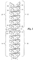
典型的なフィールド・プローブ要素の機械的な配置が、図1に示されている。電磁界プローブ要素は、チップ抵抗の4つのセット10,12,14,16からなる。チップ抵抗は、図1には図示されていないプリント基板に取付けられる。セット10,14は基板の一方の面に取付けられ、セット12,16は基板の反対面に取付けられる。
A typical field probe element mechanical arrangement is shown in FIG. The electromagnetic field probe element consists of four
抵抗は、図1に導線として示される伝導体によって電気的に接続される。図1の上部のセット10,12のチップ抵抗「a」が、伝導体18,20等により電気的に直列に接続され、セット10,12のチップ抵抗「b」が伝導体22,24等により電気的に直列に接続される。基板の一方の面のチップは、一方向へ斜めに傾いている。基板の反対側のチップは、それとは反対方向に斜めに傾いている。チップの傾斜により、各々の抵抗の最下端部が、電気的に直列に接続された次の抵抗の最上端部の正反対側に配置される。この電気的に直列に接続された抵抗の端部間の対向関係により、伝導体はプリント基板を直に通って延び、実際には、伝導体は基板上のメッキされたスルーホールの形態をとる。
The resistors are electrically connected by conductors shown as conductors in FIG. The chip resistors “a” of the
2つの抵抗列「a」及び「b」が相互に撚り合わされ、電気抵抗を有するツイストペアが形成されることが、図1より明らかとなるであろう。 It will be clear from FIG. 1 that the two resistor strings “a” and “b” are twisted together to form a twisted pair having electrical resistance.
抵抗セット14,16は、同様に、抵抗列「a」と抵抗列「b」からなり、抵抗列「a」及び「b」が相互に撚り合わされるように、電気接続が基板を通ってなされている。 The resistor sets 14 and 16 are similarly composed of a resistor string “a” and a resistor string “b”, and electrical connections are made through the substrate such that the resistor strings “a” and “b” are twisted together. ing.
図1の中間部に示されるように、抵抗チップ26(「b」チップ)は、一体化2相ダイオードパッケージ32の共通ターミナルにも接続される伝導体30によって、直接抵抗チップ28(「a」チップ)に接続される。一方のダイオードのアノードは、基板上の伝導体34を経由して、セット14の「a」抵抗36に接続される。他方のダイオードのカソードは、伝導体38を経由して、セット16の「b」抵抗40に接続される。
As shown in the middle portion of FIG. 1, the resistor chip 26 (“b” chip) is directly connected to the resistor chip 28 (“a”) by a
抵抗及びダイオードの電気配列が、図2に示されている。実際には、内部結線30より上の抵抗がダイポールの一方のアームを構成し、ダイオードの下の抵抗がダイポールの他方のアームを構成する。ダイオードから離れたいくつかの抵抗、すなわち、抵抗42〜52は、撚り合わされたフィーダとして用いられ、受信した無線信号をフレキシブル光ファイバ光伝導体56によって届けられる光信号に好適に変換する処理回路54にダイポールアンテナを接続する。光ファイバ光伝導体は電気伝導しないので、プローブのアンテナパターンへの影響は殆どない。
The electrical arrangement of resistors and diodes is shown in FIG. In practice, the resistance above the
ダイポールを構成するディスクリート抵抗の抵抗値は、動作周波数帯に亘りアンテナ全体をテーパ型抵抗ダイポールに近づくように変化することが好ましい。抵抗値は、ダイオードが位置するダイポールの中心からの距離とともに増加する。テーパ型抵抗ダイポールは、神田元久著『Standard Antennas for Electromagnetic Interference Measurements and Methods to Calibrate Them, IEEE Transactions on Electromagnetic Compatibility, Vol. 36, No. 4, November 1994』に記載されている。神田氏の論文は、参照として、ここに一体化される。 The resistance value of the discrete resistor constituting the dipole preferably changes so that the entire antenna approaches the tapered resistance dipole over the operating frequency band. The resistance value increases with the distance from the center of the dipole where the diode is located. Tapered resistance dipoles are described in Motohisa Kanda, “Standard Antennas for Electromagnetic Interference Measurements and Methods to Calibrate Them, IEEE Transactions on Electromagnetic Compatibility, Vol. 36, No. 4, November 1994”. Kanda's paper is integrated here as a reference.
例えば、抵抗26,28,36,40の標準値は、68Ωである。各列の6つの抵抗の抵抗値は、典型的には、ダイポールの中心から先端に向かって、順に、68Ω、82Ω、100Ω、150Ω、270Ω、560Ωである。これらは、約4GHzから5GHzの間の最大動作周波数を有するように設計されるプローブにおける抵抗値である。プローブの予定上限周波数に基づいて、各々のダイポールの大きさ及び抵抗の抵抗値を変動させてもよい。
For example, the standard value of the
ダイポールの中心から外に向かい抵抗値が低い値から高い値へ増加する抵抗によりダイポール要素を形成することで達成される、テーパ型抵抗負荷は、広い周波数帯で反応するプローブを提供し、アンテナの自然共振周波数の作用を抑える。各要素を構成する接近結合された複数の抵抗列を用いることで、比較的厚いダイポール要素と同様の効果を奏し、プローブの感度をさらに向上させる。 A tapered resistive load, achieved by forming a dipole element with a resistance increasing from low to high from the center of the dipole, provides a probe that responds in a wide frequency band, suppress the action of natural co-vibration frequency. By using a plurality of closely coupled resistor strings constituting each element, an effect similar to that of a relatively thick dipole element is obtained, and the sensitivity of the probe is further improved.
フィーダ抵抗42〜52は非常に高い抵抗値を有するべきであり、抵抗42,48はそれぞれ典型的には2MΩの抵抗値を有し、抵抗44,50,46,52はそれぞれ典型的には390KΩの抵抗値を有する。
Feeder resistors 42-52 should have very high resistance values,
図1に示されているように、基板の両面に抵抗を取付けることにより、抵抗列を相互に撚り合わせることができる。フィーダを形成する抵抗列は、ダイポール要素を形成する抵抗列と同様に相互に撚り合わされる。フィーダの抵抗列の撚りは、関係のない電磁場を拾うことを少なくさせる。ダイポール要素を形成する抵抗列の撚りは、長手方向軸のまわりのダイポールの回転対称性を向上させる。フィーダに隣合うダイポール要素が2つ以上の抵抗列からなることは重要であるが、勿論、フィーダから離れたダイポール要素を1つの抵抗列で構成することは可能である。しかし、両方のダイポール要素を、対称性のために同一に撚り合わされた抵抗列で形成するのが好ましい。 As shown in FIG. 1, the resistor strings can be twisted together by attaching resistors to both sides of the substrate. The resistor strings forming the feeder are twisted together like the resistor strings forming the dipole element. Twisting the feeder's resistor string makes it less likely to pick up irrelevant electromagnetic fields. The twisting of the resistor string forming the dipole element improves the rotational symmetry of the dipole about the longitudinal axis. It is important that the dipole element adjacent to the feeder is composed of two or more resistor strings. Of course, it is possible to configure a dipole element separated from the feeder by one resistor string. However, it is preferred that both dipole elements be formed of resistor strings that are twisted identically for symmetry.
ダイポールの各アームにおける抵抗列の数を変更することは、可能である。例えば、4つのダイオードがダイポールの中心に直列で(電気的に同方向に接続されて)設けられる場合、処理回路を第1ダイポールアームの二つの平行した抵抗列を経由して直列のダイオードの外端部に接続し、第3の抵抗列を第2及び第3ダイオードの接続部に一端を接続し、他端を自由端とすることで、第1ダイポールアームに第3の列を構成できる。もう一つのダイポールアームは、第1及び第2ダイオードの間及び第3及び第4ダイオードの間の接続にそれぞれ接続された2つの平行した抵抗列からなる。このように、この変更で、ダイポールは、一方のアームに3つの抵抗列を、他方のアームに2つの抵抗列を有する。 It is possible to change the number of resistor strings in each arm of the dipole. For example, if four diodes are provided in series (electrically connected in the same direction) at the center of the dipole, the processing circuit is connected to the outside of the series diode via two parallel resistor strings of the first dipole arm. By connecting one end to the connecting portion of the second and third diodes and connecting the other end to the free end, the third row can be formed on the first dipole arm. The other dipole arm consists of two parallel resistor strings connected to the connection between the first and second diodes and between the third and fourth diodes, respectively. Thus, with this change, the dipole has three resistance strings in one arm and two resistance strings in the other arm.
本発明の好適な実施形態の重要な特徴は、ダイポールの中心に、一対のダイオード58,60を設けることである。これらのダイオードは、電気的に直列に同じ方向に相互に接続されており、フィーダに隣合ってダイポール要素を形成する抵抗列と直列にそれぞれ配置される。ダイオードは、検波器としてともに作動し、ダイポールが曝される電界の強さに応じて変化する直流出力信号を処理回路54に出力する。
An important feature of the preferred embodiment of the present invention is the provision of a pair of
ダイオードからの直流信号を伝える2つの伝導体からなる給電線を有し、中心に検波器として単一のダイオードを有する抵抗ダイポールの場合には、ダイポールが180°反転すると、ダイオードが2乗領域(square law region)で作動 していない限り所定の電磁場に対して異なった応答信号を出力してしまう。 In the case of a resistance dipole having a feed line made of two conductors for transmitting a DC signal from a diode and having a single diode as a detector at the center, when the dipole is inverted by 180 °, the diode becomes a square region ( Unless it is operating in the square law region), a different response signal is output for a given electromagnetic field.
図2に示すように、本発明の好適な実施形態のダイオードは実際は相互に直列に接続されるが、直列に接続される抵抗要素においては反対方向に配置される。2つのダイオードが反対方向にある結果、対称性が得られ、ダイポールの向きが逆になったとき、すなわち、図1及び図2のダイポールが180°引っくり返りダイオードが2乗領域の外で作動している場合であっても、所定の電界に対する検出された応答信号を同一にすることができる。 As shown in FIG. 2, the diodes of the preferred embodiment of the present invention are actually connected in series with each other, but are arranged in opposite directions in series connected resistance elements. As a result of the two diodes in opposite directions, symmetry is obtained and when the dipole orientation is reversed, i.e., the dipoles in FIGS. 1 and 2 are turned over 180 ° and the diodes operate outside the square area. Even in such a case, the detected response signals for a predetermined electric field can be made the same.
中心に位置する一対のダイオードがあることで、フィーダをダイポールの外端部のうちの1つに接続でき、それにより、ダイポールの中心に接続される別のフィーダが不要になり、ダイポールのアンテナパターンの軸対称性に対する別のフィーダの悪影響を除去することができるというさらなる利点が得られる。また、中心に位置する一対のダイオードがあることで、いくつかの応用において有利な、低周波で増加された応答信号を出力できるという潜在的な利点も得られる。 The center pair of diodes allows the feeder to be connected to one of the outer ends of the dipole, thereby eliminating the need for a separate feeder connected to the center of the dipole, and the dipole antenna pattern A further advantage is that the adverse effect of another feeder on the axial symmetry of the can be eliminated. The centered pair of diodes also offers the potential advantage of being able to output an increased response signal at low frequencies, which is advantageous in some applications.
前述したように、ダイポールのディスクリート抵抗とフィーダを基板上へ取付けると、相互に撚り合わされ、接近結合された一対の抵抗伝導体を具えたダイポールを簡便に提供することができる。また、それにより、処理回路、ダイポール及びフィーダ抵抗を、図3及び図4に示すように、単一の基板上に取付けることができる。基板は、図3に示すように、処理回路の様々な構成要素が取付けられる広い部分64の一端から外に向かって延びる、細長く狭い部分62を有して形成してもよい。典型的なプローブにおいて、処理回路は、増幅回路及び圧縮回路を有し、信号を光ファイバ光伝導体56(図2)経由でコンピューターで利用可能なフォーマットに変換するA/D変換器(図示せず。)に伝えることができるように、ダイポールの直流応答信号を光信号に変換する変換器を有する。
As described above, when the discrete resistance of the dipole and the feeder are mounted on the substrate, a dipole having a pair of resistance conductors twisted together and closely coupled can be provided. It also allows the processing circuit, dipole and feeder resistance to be mounted on a single substrate as shown in FIGS. The substrate may be formed with an elongated
いくつかの方法で、処理回路へ電力を供給することができる。例えば、バッテリ電源を有してもよいし、外部レーザー又はその他の光源から光伝導体を通して処理回路に伝わる光線により通電される基板上の光電池から電力を得てもよい。 Power can be supplied to the processing circuit in several ways. For example, it may have a battery power source, or it may obtain power from a photovoltaic cell on the substrate that is energized by light rays traveling from an external laser or other light source through the photoconductor to the processing circuit.
1軸プローブの場合、図5に示すように、処理回路をハウジング65内で有してもよい。
In the case of a single-axis probe, a processing circuit may be provided in a
3つの軸における電界を計測できるように、複数のプローブは3つの相互に直交するダイポールを有するプローブとして一体化させることができる。 A plurality of probes can be integrated as a probe having three mutually orthogonal dipoles so that electric fields in three axes can be measured.
そのような一体化が図6に示されており、ダイポール66,68,70は処理回路を具えた球面ハウジング72からx、y及びz軸に沿ってそれぞれ延びる。ダイポール66,68は、単一のプリント基板上に形成することができる。
Such an integration is illustrated in FIG. 6, where
図7に示されるもう1つの三次元電界プローブは、図5に示される型の3つの別々のプローブ74,76,78を有し、それらは、相互に直交するように配置され、互いにダイポールの中心の辺りで交差する。
The other three-dimensional electric field probe shown in FIG. 7 has three
上記のプローブにおいて、様々な変更が可能である。例えば、フィーダを形成するディスクリート抵抗の数と同様に、各々のダイポールを形成するディスクリート抵抗の数を変えることができる。処理回路が小さい場合、フィーダ抵抗の数を減らすこともできるし、フィーダを完全に省くこともできる。 Various modifications can be made to the above probe. For example, the number of discrete resistors that form each dipole can be varied, as can the number of discrete resistors that form a feeder. If the processing circuit is small, the number of feeder resistors can be reduced or the feeder can be omitted completely.
例えば、撚り合わされたディスクリート抵抗からなるダイポールアームで、フィーダをダイポールアームの外端に接続させない等の本発明の特定の特徴から利点が得られる。例えば、処理回路を小さくする場合、ダイポールアームの端ではなく、ダイポールの中心近くに処理回路を置くことが可能である。さらに、非常に小さい処理回路が使われる場合、処理回路をダイポールの中心の位置の基板上に設けることができる。 Advantages may be obtained from certain features of the present invention, such as, for example, a dipole arm consisting of twisted discrete resistors, with no feeder connected to the outer end of the dipole arm. For example, when the processing circuit is made small, it is possible to place the processing circuit near the center of the dipole instead of the end of the dipole arm. Further, if a very small processing circuit is used, the processing circuit can be provided on the substrate at the center of the dipole.
さらに、特許請求の範囲に記載の本発明の範囲内から逸脱しない、上記の装置及び方法のその他の変更が可能である。 Furthermore, other modifications of the above-described apparatus and method are possible without departing from the scope of the invention as set forth in the claims.
Claims (10)
Applications Claiming Priority (2)
| Application Number | Priority Date | Filing Date | Title |
|---|---|---|---|
| US09/968,816 US6593896B2 (en) | 2001-10-01 | 2001-10-01 | Field probe |
| PCT/US2002/031930 WO2003030299A1 (en) | 2001-10-01 | 2002-09-26 | Field probe |
Publications (3)
| Publication Number | Publication Date |
|---|---|
| JP2005505962A JP2005505962A (en) | 2005-02-24 |
| JP2005505962A5 JP2005505962A5 (en) | 2005-12-22 |
| JP4068559B2 true JP4068559B2 (en) | 2008-03-26 |
Family
ID=25514814
Family Applications (1)
| Application Number | Title | Priority Date | Filing Date |
|---|---|---|---|
| JP2003533377A Expired - Fee Related JP4068559B2 (en) | 2001-10-01 | 2002-09-26 | Field probe |
Country Status (8)
| Country | Link |
|---|---|
| US (1) | US6593896B2 (en) |
| EP (1) | EP1436855B1 (en) |
| JP (1) | JP4068559B2 (en) |
| KR (1) | KR100650292B1 (en) |
| CN (1) | CN1561562A (en) |
| AT (1) | ATE366463T1 (en) |
| DE (1) | DE60221034D1 (en) |
| WO (1) | WO2003030299A1 (en) |
Families Citing this family (6)
| Publication number | Priority date | Publication date | Assignee | Title |
|---|---|---|---|---|
| NL2000793C2 (en) | 2007-08-03 | 2009-02-09 | Dijkstra Advies | Probe for measuring an electric field. |
| US8305282B2 (en) * | 2010-07-23 | 2012-11-06 | Amplifier Research Corporation | Field probe |
| FR2967827B1 (en) * | 2010-11-24 | 2013-08-02 | Univ Rennes | BROAD BANDWIDTH COMMUNICATION ANTENNA. |
| US20130307763A1 (en) * | 2012-05-21 | 2013-11-21 | Amplifier Research Corporation | Field analyzer |
| CN106483387A (en) * | 2016-11-16 | 2017-03-08 | 中国电子科技集团公司第四十研究所 | A kind of electric field radiation broadband detector and its detection method |
| US11454661B2 (en) | 2020-11-05 | 2022-09-27 | Amplifier Research Corp. | Field probe |
Family Cites Families (12)
| Publication number | Priority date | Publication date | Assignee | Title |
|---|---|---|---|---|
| US3662260A (en) | 1971-02-12 | 1972-05-09 | Us Navy | Electric field measuring instrument with probe for sensing three orthogonal components |
| US3750017A (en) * | 1971-09-16 | 1973-07-31 | Us Health | Electromagnetic field measuring device |
| US3906509A (en) * | 1974-03-11 | 1975-09-16 | Raymond H Duhamel | Circularly polarized helix and spiral antennas |
| US4008477A (en) * | 1975-06-25 | 1977-02-15 | The United States Of America As Represented By The Secretary Of Commerce | Antenna with inherent filtering action |
| US4207518A (en) * | 1978-03-06 | 1980-06-10 | General Microwave Corporation | Broadband radiation detector with diode elements |
| US4466003A (en) * | 1982-02-09 | 1984-08-14 | The United States Of America As Represented By The Secretary Of The Navy | Compact wideband multiple conductor monopole antenna |
| US4634968A (en) * | 1982-12-20 | 1987-01-06 | The Narda Microwave Corporation | Wide range radiation monitor |
| US5644321A (en) | 1993-01-12 | 1997-07-01 | Benham; Glynda O. | Multi-element antenna with tapered resistive loading in each element |
| US6061025A (en) * | 1995-12-07 | 2000-05-09 | Atlantic Aerospace Electronics Corporation | Tunable microstrip patch antenna and control system therefor |
| US6084551A (en) | 1998-01-21 | 2000-07-04 | L-3 Communications, Inc. | Electromagnetic probe for the detection of e-field and h-field radiation |
| US6239749B1 (en) * | 1999-01-29 | 2001-05-29 | Ching-Kuang Tzuang | Fast-wave resonant antenna with stratified grounding planes |
| DE10114012B4 (en) * | 2000-05-11 | 2011-02-24 | Amtran Technology Co., Ltd., Chung Ho | chip antenna |
-
2001
- 2001-10-01 US US09/968,816 patent/US6593896B2/en not_active Expired - Fee Related
-
2002
- 2002-09-26 DE DE60221034T patent/DE60221034D1/en not_active Expired - Lifetime
- 2002-09-26 JP JP2003533377A patent/JP4068559B2/en not_active Expired - Fee Related
- 2002-09-26 CN CNA028193083A patent/CN1561562A/en active Pending
- 2002-09-26 EP EP02773721A patent/EP1436855B1/en not_active Expired - Lifetime
- 2002-09-26 WO PCT/US2002/031930 patent/WO2003030299A1/en active IP Right Grant
- 2002-09-26 KR KR1020047004821A patent/KR100650292B1/en not_active IP Right Cessation
- 2002-09-26 AT AT02773721T patent/ATE366463T1/en not_active IP Right Cessation
Also Published As
| Publication number | Publication date |
|---|---|
| KR100650292B1 (en) | 2006-11-27 |
| EP1436855A1 (en) | 2004-07-14 |
| ATE366463T1 (en) | 2007-07-15 |
| DE60221034D1 (en) | 2007-08-16 |
| EP1436855A4 (en) | 2005-02-02 |
| US20030063039A1 (en) | 2003-04-03 |
| US6593896B2 (en) | 2003-07-15 |
| EP1436855B1 (en) | 2007-07-04 |
| KR20040037231A (en) | 2004-05-04 |
| JP2005505962A (en) | 2005-02-24 |
| WO2003030299A1 (en) | 2003-04-10 |
| CN1561562A (en) | 2005-01-05 |
Similar Documents
| Publication | Publication Date | Title |
|---|---|---|
| US4480223A (en) | Unitary probe assembly | |
| US7298140B2 (en) | Three-dimensional magnetic direction sensor, and magneto-impedance sensor element | |
| KR100959599B1 (en) | Probe for high frequency signal transmission and probe card using the same | |
| US5373231A (en) | Integrated circuit probing apparatus including a capacitor bypass structure | |
| US6515499B1 (en) | Modular semiconductor tester interface assembly for high performance coaxial connections | |
| JP2009537828A (en) | Multi-channel signal acquisition probe | |
| JP2005010147A (en) | Module with inspection function, and its inspection method | |
| JP4068559B2 (en) | Field probe | |
| US3721900A (en) | Microwave detection instrument and antenna therefor | |
| JP5572066B2 (en) | Test board | |
| TW201142299A (en) | Probe card | |
| TW200831912A (en) | High frequency probe assembly for IC testing | |
| JP2734412B2 (en) | Semiconductor device socket | |
| JP2004333459A (en) | Contact probe, and semiconductor and electrical inspection device using the same | |
| CN214427506U (en) | PCB level current sensor | |
| CN205898905U (en) | Dipole antenna and use this dipole antenna's omni -direction probe | |
| JPS62106379A (en) | Magnetic field measuring probe | |
| US6731124B2 (en) | Integrated device for testing contacts | |
| US6411113B1 (en) | Radio frequency test fixture | |
| KR100241362B1 (en) | Plane-type magnetic probe | |
| KR20160091847A (en) | A Dipole Antenna | |
| JPS6171367A (en) | Fixed probe card | |
| CN101788573A (en) | Probe card | |
| US5777470A (en) | Broadband probe for detecting the magnetic field component of an electromagnetic field | |
| US20190353682A1 (en) | Surface-mountable apparatus for coupling a test and measurement instrument to a device under test |
Legal Events
| Date | Code | Title | Description |
|---|---|---|---|
| A977 | Report on retrieval |
Free format text: JAPANESE INTERMEDIATE CODE: A971007 Effective date: 20060919 |
|
| A131 | Notification of reasons for refusal |
Free format text: JAPANESE INTERMEDIATE CODE: A131 Effective date: 20061003 |
|
| A601 | Written request for extension of time |
Free format text: JAPANESE INTERMEDIATE CODE: A601 Effective date: 20061225 |
|
| A602 | Written permission of extension of time |
Free format text: JAPANESE INTERMEDIATE CODE: A602 Effective date: 20070105 |
|
| A521 | Request for written amendment filed |
Free format text: JAPANESE INTERMEDIATE CODE: A523 Effective date: 20070403 |
|
| TRDD | Decision of grant or rejection written | ||
| A01 | Written decision to grant a patent or to grant a registration (utility model) |
Free format text: JAPANESE INTERMEDIATE CODE: A01 Effective date: 20071218 |
|
| A61 | First payment of annual fees (during grant procedure) |
Free format text: JAPANESE INTERMEDIATE CODE: A61 Effective date: 20080110 |
|
| FPAY | Renewal fee payment (event date is renewal date of database) |
Free format text: PAYMENT UNTIL: 20110118 Year of fee payment: 3 |
|
| R150 | Certificate of patent or registration of utility model |
Free format text: JAPANESE INTERMEDIATE CODE: R150 |
|
| FPAY | Renewal fee payment (event date is renewal date of database) |
Free format text: PAYMENT UNTIL: 20120118 Year of fee payment: 4 |
|
| FPAY | Renewal fee payment (event date is renewal date of database) |
Free format text: PAYMENT UNTIL: 20130118 Year of fee payment: 5 |
|
| R250 | Receipt of annual fees |
Free format text: JAPANESE INTERMEDIATE CODE: R250 |
|
| R250 | Receipt of annual fees |
Free format text: JAPANESE INTERMEDIATE CODE: R250 |
|
| R250 | Receipt of annual fees |
Free format text: JAPANESE INTERMEDIATE CODE: R250 |
|
| LAPS | Cancellation because of no payment of annual fees |