JP4053651B2 - Electromagnetic radiation detector, high-sensitivity pixel structure using the detector, and method of manufacturing the detector - Google Patents
Electromagnetic radiation detector, high-sensitivity pixel structure using the detector, and method of manufacturing the detector Download PDFInfo
- Publication number
- JP4053651B2 JP4053651B2 JP06757598A JP6757598A JP4053651B2 JP 4053651 B2 JP4053651 B2 JP 4053651B2 JP 06757598 A JP06757598 A JP 06757598A JP 6757598 A JP6757598 A JP 6757598A JP 4053651 B2 JP4053651 B2 JP 4053651B2
- Authority
- JP
- Japan
- Prior art keywords
- region
- layer
- detector
- dopant concentration
- pixel structure
- Prior art date
- Legal status (The legal status is an assumption and is not a legal conclusion. Google has not performed a legal analysis and makes no representation as to the accuracy of the status listed.)
- Expired - Lifetime
Links
- 230000005670 electromagnetic radiation Effects 0.000 title claims description 12
- 238000004519 manufacturing process Methods 0.000 title claims description 5
- 239000000758 substrate Substances 0.000 claims abstract description 69
- 230000004888 barrier function Effects 0.000 claims abstract description 41
- 239000002800 charge carrier Substances 0.000 claims abstract description 38
- 239000004065 semiconductor Substances 0.000 claims abstract description 35
- 230000005855 radiation Effects 0.000 claims abstract description 26
- 238000000034 method Methods 0.000 claims description 37
- 239000002019 doping agent Substances 0.000 claims description 23
- 238000009792 diffusion process Methods 0.000 claims description 20
- 239000007943 implant Substances 0.000 claims description 16
- 230000008569 process Effects 0.000 claims description 16
- 238000001514 detection method Methods 0.000 claims description 14
- 238000002347 injection Methods 0.000 claims description 8
- 239000007924 injection Substances 0.000 claims description 8
- 230000006798 recombination Effects 0.000 claims description 7
- 238000005215 recombination Methods 0.000 claims description 7
- 238000012546 transfer Methods 0.000 claims description 2
- 230000004044 response Effects 0.000 claims 2
- 238000001444 catalytic combustion detection Methods 0.000 description 17
- 239000003990 capacitor Substances 0.000 description 12
- 238000002513 implantation Methods 0.000 description 12
- 238000005516 engineering process Methods 0.000 description 9
- 230000000694 effects Effects 0.000 description 8
- 230000003287 optical effect Effects 0.000 description 7
- 239000002184 metal Substances 0.000 description 6
- 230000003321 amplification Effects 0.000 description 5
- 230000006870 function Effects 0.000 description 5
- 238000003199 nucleic acid amplification method Methods 0.000 description 5
- 238000005468 ion implantation Methods 0.000 description 4
- 239000011159 matrix material Substances 0.000 description 4
- XUIMIQQOPSSXEZ-UHFFFAOYSA-N Silicon Chemical compound [Si] XUIMIQQOPSSXEZ-UHFFFAOYSA-N 0.000 description 3
- 239000004020 conductor Substances 0.000 description 3
- 239000013078 crystal Substances 0.000 description 3
- 238000000605 extraction Methods 0.000 description 3
- 238000003384 imaging method Methods 0.000 description 3
- 230000006872 improvement Effects 0.000 description 3
- 238000005259 measurement Methods 0.000 description 3
- 229910021420 polycrystalline silicon Inorganic materials 0.000 description 3
- 229920005591 polysilicon Polymers 0.000 description 3
- 229910052710 silicon Inorganic materials 0.000 description 3
- 239000010703 silicon Substances 0.000 description 3
- 238000000342 Monte Carlo simulation Methods 0.000 description 2
- 238000013461 design Methods 0.000 description 2
- 239000003574 free electron Substances 0.000 description 2
- 230000010354 integration Effects 0.000 description 2
- 239000000463 material Substances 0.000 description 2
- 230000007246 mechanism Effects 0.000 description 2
- 238000001465 metallisation Methods 0.000 description 2
- 238000005036 potential barrier Methods 0.000 description 2
- 238000011160 research Methods 0.000 description 2
- 230000035945 sensitivity Effects 0.000 description 2
- 238000004088 simulation Methods 0.000 description 2
- 238000003860 storage Methods 0.000 description 2
- 229910008065 Si-SiO Inorganic materials 0.000 description 1
- 229910004298 SiO 2 Inorganic materials 0.000 description 1
- 229910006405 Si—SiO Inorganic materials 0.000 description 1
- 238000003491 array Methods 0.000 description 1
- 230000006399 behavior Effects 0.000 description 1
- 230000015572 biosynthetic process Effects 0.000 description 1
- 230000015556 catabolic process Effects 0.000 description 1
- 230000008859 change Effects 0.000 description 1
- 238000006243 chemical reaction Methods 0.000 description 1
- 238000012937 correction Methods 0.000 description 1
- 230000001066 destructive effect Effects 0.000 description 1
- 238000010586 diagram Methods 0.000 description 1
- 238000001914 filtration Methods 0.000 description 1
- 238000005286 illumination Methods 0.000 description 1
- 239000012212 insulator Substances 0.000 description 1
- 239000002245 particle Substances 0.000 description 1
- 230000035515 penetration Effects 0.000 description 1
- 238000012545 processing Methods 0.000 description 1
- 230000000644 propagated effect Effects 0.000 description 1
- 238000012216 screening Methods 0.000 description 1
- 230000002123 temporal effect Effects 0.000 description 1
Images


Classifications
-
- H—ELECTRICITY
- H01—ELECTRIC ELEMENTS
- H01L—SEMICONDUCTOR DEVICES NOT COVERED BY CLASS H10
- H01L22/00—Testing or measuring during manufacture or treatment; Reliability measurements, i.e. testing of parts without further processing to modify the parts as such; Structural arrangements therefor
-
- H—ELECTRICITY
- H01—ELECTRIC ELEMENTS
- H01L—SEMICONDUCTOR DEVICES NOT COVERED BY CLASS H10
- H01L27/00—Devices consisting of a plurality of semiconductor or other solid-state components formed in or on a common substrate
- H01L27/14—Devices consisting of a plurality of semiconductor or other solid-state components formed in or on a common substrate including semiconductor components sensitive to infrared radiation, light, electromagnetic radiation of shorter wavelength or corpuscular radiation and specially adapted either for the conversion of the energy of such radiation into electrical energy or for the control of electrical energy by such radiation
- H01L27/144—Devices controlled by radiation
- H01L27/146—Imager structures
- H01L27/14643—Photodiode arrays; MOS imagers
Abstract
Description
【0001】
【発明の属する技術分野】
本発明は、半導体を基礎とする電磁放射用検出器の分野に関する。更には、広い放射検出区域又は高いフィルファクタを備えた半導体検出器及び半導体ピクセル構造に関する。
本発明は、また、そのような検出器の製造方法に関する。
【0002】
【従来の技術】
半導体を基礎とするセンサ及び電磁放射を検出するデバイスは、よく知られている。例えば、EP−A−739039及びWO93/19489に述べられたようなセンサである。それらのセンサは、CMOS又はMOS技術により形成される。それらのセンサにおいて、半導体基板中の放射により発生した電荷キャリアを集めるために付加された領域は、p−n又はn−p接合から形成され、基板は、夫々、n型導電体又はp型導電体から形成される。かかる接合は、コネクション接合と呼ばれる。CMOS又はMOS技術を用いて形成されたイメージセンサにおいて、受動ピクセルを備えたCMOS又はMOSイメージセンサと、能動ピクセルを備えたCMOS又はMOSイメージセンサとは、区別されている。EP−A−739039又はWO93/19489のセンサは、能動ピクセルセンサである。
【0003】
【発明が解決しようとする課題】
能動ピクセルセンサは、電荷の増幅のためのピクセルを集積した手段を備えるように形成され、かかる電荷は、光感受性エレメント又はピクセル中の構成により集められる。受動ピクセルは、そのような手段を有さず、電荷感度増幅器を必要とし、これはピクセルの中に集積化されずにピクセルに対して長い配線により接続される。能動ピクセルの付加的な電気成分により、能動ピクセルイメージセンサは、より精巧な機能を果たすように形成され、イメージングデバイス又はそのセンサに基づくシステムの性能において、優れることができる。かかる機能は、フィルタリング、高速動作、又はより照度の高い状態での動作を含むことができる。
しかしながら、能動ピクセルCMOS又はMOSイメージセンサには、大きな欠点がある。かかる欠点は、より少ないが、受動ピクセルセンサにも存在する。それは、ピクセルの表面の重要な部分が、読み出し回路に用いられるということである。
【0004】
p−n又はn−p接合の電荷検知体積(Volume)が、かかる接合の空乏層よりも広いということがよく知られている。実際に、コレクション接合から再結合長と呼ばれる範囲内で発生したすべての電荷は、かかる接合に拡散して集められる機会を有する。このメカニズムに基づくと、小さな接合と、広い光検知体積とを有するセンサを形成することは可能である。光センサは、3×2μmの接合と、15μmの再結合長とを備えることができる。このように、かかる検知器は、外観上、表面サイズ又は光検知領域が30μmの直径を有する。
しかしながら、もし、関係のない電気的回路、例えば、引き出し回路が、そのようなコレクション接合に隣合って設けられた場合、そのコレクション接合に達するべき電荷の一部がその読み出し回路の接合又は構造により集められる。そこからの読出し回路に用いられる検知器の領域上に注いだ光により発生する電荷キャリアは、主に、かかる読出し回路の接合により集められる。ピクセル中の読出し回路に取られる区域は、放射を集めることを損ない、これは、センサに基づく能動ピクセルの低いフィルファクタ又は低い感度の原因となる。
【0005】
”Solid-State Imaging with Charge Coupled Devises、A.THeuwissen (Kluwer Academic publishers, 1995 ISDN 0-7923-3456-6)”の本の中では、半導体を基礎とするイメージデバイスの現状について概説されている。例えば、CCDやMOSカメラについである。この本の第7章には、ピクセルのフィルファクタ又は感度を増加させるトピックスについて述べられている。かかる方法は、マイクロレンズの使用や光変換トップレイヤーの使用によるものである。
【0006】
”XYW detector a smart two-dimensional particle detector、Bart Dierckx”(Nuclear Instruments and Methods in Physics Research, vol. A275 (1989), p.542-544)の論文の図4には、半導体に基づくピクセルデバイスの4つの形成方法について述べられている。第1の方法は、古典的なCMOSプロセスに基づくものである。この方法の欠点は、低いフィルファクタであり、これは読み出し電気回路により半導体表面の一部分が覆われるためである。かかるフィルファクタの問題を解決するために提案された他の方法では、一般的ではないCMOS技術を用いて問題解決が図られている。即ち、フリップチップ(バンプボンディング)、SOI(シリコン−オン−インシュレータ)技術、又は光子検知ゾーンをアモルファストップレイヤ上に移動させる技術である。
【0007】
”Design and Performance of semiconductor detectors with integrated amplification and charge storage capability、P.Klein & al”(Nuclear Instruments and Methods in Physics Research, vol. A305 (1991), p.517-526)の論文の図2には、トランジスタ接合を用いた半導体を基礎とするセンサが示されている。ここでは、半導体基板中で生成された電荷が、接合を基礎とするバリアにより、トランジスタのソース及びドレイン接合中へ拡散するのを妨げられ、ゲートに押し込められる。かかるゲートは、ソース及びドレインと接触している。
【0008】
アバランシェ・フォト・ダイオード(APD)はより知られたものである。APDは、p++/p−/p+/n++の連続した層構造を有し、p++層は裏面コンタクト、p−層は検知層、p+層は電子のアバランシェ増幅を提供するための層、及びn++層は増殖された電子を最終的に集める層となっている。かかる増殖層のドーピング量及び幅は、大変厳密である。更に、かかる構造に印加される電圧は、かなり高いものであり、かかる構造の電気的ブレークダウンに近い値である。p−/p+層の接合部は、電子の拡散のバリアとしては働かず、アバランシェ増幅デバイスとして働く。
【0009】
そこで、本発明は、電磁放射検知用の半導体デバイスであって、半導体中で放射により形成された電荷キャリアのすべてがコレクティング接合又は領域中に集められ、読み出し回路の接合又は領域には集められない構造を提供することを目的とする。
【0010】
【課題を解決するための手段】
本発明は、第1に半導体基板を含む電磁放射用検知器に関するものであり、かる基板は、第1及び第2の領域を含む。該第1の領域及び第2の領域は、基板中で放射により形成された電荷キャリアを集めるために取り付けられる。かかる基板は、更に、かかる第2の領域への電荷の拡散を十分に防止できるバリアを形成する第3の領域を含む。
基板及びかかる第1の領域の間では、バリアは存在しないか、あるいはほとんどゼロのバリアが存在するか、又は第2の領域と基板との間のバリアよりも十分に低いバリアが存在する。
上記第3の領域も、かかる電荷キャリアが第1の領域に拡散するために十分に低いバリアを形成することができる。
【0011】
更には、本発明は、小さいが、効果的なバリアを、半導体基板中の放射検知体積と、読出し回路を備えた領域又は接合との間に備えた、放射検知器に関するものである。そしてかかる検知器は、半導体中の放射検知体積と、放射により形成された電荷キャリアを集めるために付加された領域及び接合と、の間に、バリアを有しないか又は低いバリアを有するものである。
【0012】
本発明の第1の見地によれば、第2の領域に隣接し、特にその下部にある基板により発生した電荷キャリアのいくらかの部分は、かかる第1の領域により集められる。かかる基板は、第1導電型のドーパントを有し、かかる第1領域及び第2領域は、他の第2導電型のドーパントを有する。第3の領域は、第1の導電型を有し、その第3領域のドーピング量は、基板のドーピング量よりも高い。
【0013】
本発明の第2の見地によれば、第1領域は基板との間に接合を形成し、第2の領域は第3の領域との間に接合を形成する。
【0014】
更に、本発明の他の見地によれば、本発明の検知器を含む光を検知するMOSを基礎とするピクセル構造が述べられている。この場合、第3の領域は、第2の領域に電子又はホールが拡散することを防止するのに十分な電気的バリアを形成する。かかる電気的バリアは、第3の領域及び基板の界面に形成することができる。
かかる基板から第1の領域に電子又はホールが拡散するために十分に低い電気的バリアが、第1の領域及び基板の界面に形成される。第2の領域は、第1の領域での荷電キャリアにより発生した信号を処理するための回路の部分である。かかる信号は、第1の領域で生成された電流となる。ピクセル構造は、更に、かかる第1領域及び基板に隣接する第4の領域を含むこともできる。そしてかかる第4の領域と基板の間には、基板の界面には十分に低いバリアが形成される。
【0015】
本発明の他の見地によれば、電磁放射検知用CMOSピクセル構造の製造方法及び動作方法について述べられている。
【0016】
本発明は、更には、CMOSピクセル構造及びセンサの発明、及びCCD又はCCD類似の構造の発明の設計集積化の原理に関するものも含む。本発明は、低雑音光検知に応用するために大きな利点を有している。
【0017】
【発明の実施の形態】
本発明は、半導体基板中の放射検知体積と、読出し回路を備えた領域及び接合との間の、小さいが効果的なバリアを備えた検知器や半導体検知器に関するものである。
また、本発明は、半導体中の放射検知体積と放射により生み出された電荷キャリアを集めるために設けられた領域及び接続との間の、存在しないかあるいは大変低いバリアを備えた検知器に関するものである。電荷が生成される放射検知体積と、引き出し回路の関係を有さない電気部と、の間にバリアを形成する領域は、放射検知体積と同じ導電型のドーパントを備えることができる。
【0018】
本発明の検知器は、放射により生成された電荷キャリアを集めるコレクション接合と他の電気的部分から構成される。かかるコレクション接合は、かかる他の電気的構成の下部に隣接する放射検知体積中に形成された電荷キャリアを集めるのを高める。かかる機能は、他の電気的構成部分の下部のかかる体積と同じ導電型を備えた領域との界面に形成された電気的バリア手段により形成される。かかるバリアは、他の電気的構成部分の下部で形成された電荷キャリアが他の電気的構成部分の接合又は構造中に拡散することを防止する。この電気的バリアは、コレクション接合の下部には存在しないか、あるいは十分に低いものである。その結果として、他の電気的構成部分の下で生成された電荷キャリアが集められることとなる。
【0019】
かかる検知器は、CMOSプロセスにより実現され、構成はp型基板からなり、電気的バリアを形成する領域はp+型注入として実現される。他の構成部分は、さまざまな導電型、即ち、n型接合を含んで形成される。コレクション接合は、基板に対して低い電気的バリアを備えたn型領域から形成される。より低いか、又は形成されないバリアの区域は、コレクション接合と一致し、一部又は完全に一致し、又はその一部からなる。低いか、あるいは存在しないバリアは、コレクション接合の区域へのn型注入の追加により実現することができる。又は、その電気的バリアを実現するp+型注入を行なわないことにより実現することができる。
かかるp+型注入は、pウエル注入と呼ばれるものであり、又はアンチパンチスルー注入と呼ばれるものであり、あるいはブランケット注入と呼ばれるものでありあるいはVth調整注入と呼ばれるものである。これらはCMOSプロセスにおいてほぼ同様の効果を有しCMOSプロセスの標準的な工程として多くの場合役に立つ。
【0020】
かかるn型注入は、nウエル注入と呼ばれるものであり、あるいはアンチパンチスルー注入と呼ばれるものであり、あるいはブランケット注入と呼ばれるものであり、あるいはVth調整注入と呼ばれるものである。
【0021】
本発明の代わりの具体例では、コレクション接合であってより深いn型注入又はp+p−バリアの形成を行なわないコレクション接合を備えたピクセル構造の部分を形成する検知器が、MOSFETの1の電極(ソース又はドレイン)として実現される。そして、他の電極は、一定の電圧に保たれる。正確な電圧は適切でない。即ち、他の電極は、フローティングノードでなければ良い。コレクション接合は、MOSFETのゲートによって、好ましくは完全に又は部分的に囲まれる。他の電極は、完全に又は部分的にゲート及び第1の電極を囲む。MOSFETのゲートはオフにバイヤスされ、双方の電極は電気的に絶縁される。MOSFETゲート及び接合を囲む他の電極は、接合エッジ効果による暗電流の部分を減少させる。
【0022】
本発明の原理は、CCD又はCCD類似の構造(フォトゲート、チャージインゼクションデバイス(CID)、チャージスイープデバイス(CSD))に応用することができ、かかる構造においては、コレクティング接合が反転層又はCCD電極下部の埋め込みチャネルからなる。即ち、表面チャネルCCD又は埋め込みチャネルCCDである。コレクション接合又はその一部は、そのような構造で置き換えることも可能である。
【0023】
本発明で説明する方法では、本発明は、結局、EP−A−0739039に述べられているようなピクセル構造を備えたCMOS光検知センサのような手段により説明される。EP−A−0739039は、ここに、添付文献として添付される。
結局、例として述べられたところによると、半導体基板は、p型導電体と仮定されている。しかし、かかる記述から当業者であればn型導電体の半導体基板を想像することは容易である。他の均等の具体例は、当業者にとっては明らかであり、本発明の精神及び見地は、添付した請求の範囲の文言に限定されるものではない。
【0024】
図1(A)は、p型ドーピングを備えた半導体基板6を備えたピクセル構造の一部を示す。p層又は領域5は、かかる基板中に限定される。基板は代わりの具体例においては、均一なp−又はp++ドーピングにより形成される。p−層は、拡散又はイオン注入又は結晶成長又はCMOS技術で知られた他の技術により限定される。更に加えたp+層又は領域3は、かかるp−層基板中又は基板上に限定される。p+領域は、拡散により又はイオン注入又は結晶成長又はCMOSプロセスで知られた他の技術により限定される。
【0025】
p+領域3中に、第1の領域1及び第2の領域2が限定される。かかる第1及び第2の領域は、n型ドーピングからなる。これらの第1及び第2の領域は、イオン注入又は拡散又はCMOSプロセスにより知られた他の技術により限定される。これらの第1及び第2の領域は、p型領域及び/又は基板とで接合を形成する。第1領域1は、基板中及び/又はp−領域(6、5)中で放射により生成される電荷キャリアを集めるためのコレクション接合を形成する。この例によると、コレクション接合は、フォトダイオードである。第2の領域2は、第1の領域1により集められた電荷キャリアにより発生する信号を導く引き出し電極の部分の接合を形成する。
【0026】
更には、付加的に、n型の第4領域4を形成し、第1領域1を完全に又は部分的に覆うことも可能である。かかる第4領域は、第1領域からp−領域及び/又は基板へと延びる。この第4領域は、好ましくは深いイオン注入工程により限定されることが好ましいが、CMOSプロセスで知られた他の技術により限定されるものであっても構わない。
【0027】
図1(B)は、図1(A)に示した構造の他の具体例を示す。
図2及び3は、図1に示した構造の第1及び第2に沿った断面における電気的ポテンシャルを示すものである。
図1に示された構造においては、図2及び3に示されるように、p−領域に部分的ポテンシャルの最少を有する。図2に示すようにp+領域3により形成された界面(3/5)における電気的バリアにより、p−領域の電子は第2領域2の中には容易には拡散しない。図3によれば、電子は、p−領域5及びn+領域1の間のバリアによっては妨げられない。ゾーンI中の電子はゾーンIIに拡散し、第1領域1で集められることは明らかである。図1に概略を模式的に示した構造中の電荷キャリアの拡散は、モンテ・カルロ・シミュレーションに基づいてシミュレートされた。かかるシミュレーション結果を図4に示す。
【0028】
本発明によるピクセルのマトリックスで、放射により発生した電子がランダムワークすることがシミュレートされている。ピクセルは、図1(A)に示す構造に基づき形成される。電子の平均拡散距離が記録される。第4領域4が存在しない(すなわち従来構造)構造における拡散距離は大きく電子は集められるか、あるいはホールと再結合する前に、多くのピクセルを拡散する。第4の領域4を有する構造においては、電子はずっと速く集められる。かかる結果を以下の表に示す。表は、7.5×7.5μmのピッチで形成されたピクセルのピクセルマトリックスについてシミュレートされ、各ピクセル中には第1及び第4領域がさまざまなサイズで形成されたものである。電子は、最も悪い場合においては、4つのピクセルの間の端部において生成する。
【0029】
【表1】

結果的な拡散距離は、理想的な結果(3.75μm)に近くなる。この種類のピクセルは、このように理想に近いモジュレーショントランスファーフアンクション(MTF)を備える。それは、ほぼ100%のフィルファクタを有し、このことは光に晒されるピクセルマトリックスのすべての表面が、光の収集に寄与することを意味する。
実際に光により生成される基板電荷キャリアのすべてがコレクション接合に流れる。従来技術のピクセル構造においては、生成された電荷キャリアの一部は引き出し回路の接続により収集されこのような電荷は消失していた。
【0031】
領域3の導入は多くの効果を持つがそれらの2つは以下の通りである。
フォトダイオード1、4−5、6は、すべてのピクセルからの光電荷を集め100%のフィルファクタに到達することができる。フォトダイオードは、すべてのピクセルからの光電荷を集め、フィルファクタは単に以下の3つの要素によってのみ制限されるにすぎない。
▲1▼ 引き出し回路、それ自身の接続の内部の光トラップ。これは短い波長に対して確かに制限となり低い浸透深さを備える。
▲2▼ 接合部金属による光の反射。
▲3▼ 再結合。自由電子は不明瞭には拡散せず一定の典型的な再結合長さの後に再結合する。CMOS技術においては、この長さがピクセルピッチの数倍を越える。
【0032】
第2はイメージの鮮明さ又はMTFである。領域3が基板及びコレクション接合1の間に存在するような場合においては、領域3と基板との界面において電荷キャリアの拡散のためのバリアを形成する領域3があり、これがコレクション接合1により電荷キャリアが容易に集められることを妨げる。自由電子は隣のピクセルに拡散するための時間を有し、結局そこで集められる又は再結合し、イメージの不鮮明さを引き起こす。フォトダイオード中の領域4の限定によるこのようなバリアの省略は、光電荷を低減することとなる。
【0033】
発明の好ましい具体例
標準的なCMOSプロセスにおいて、フォトダイオードの小さな2つのアレイ(A、B)が、集積回路の部分として形成される。(A)の場合、接合は従来技術のようにp型基板中の浅いn型領域からなる。接合寸法は、2×2μmであり、ピクセルピッチは7.5μmである。ピクセルアレイの中央の列は光に晒され、ピクセルの隣接した列は金属シールドにより光から遮断される。ピクセルの列の平行した出力は、集積回路の外部に設けられ、ピクセルの列の効果的な光電流が測定できる。
【0034】
(B)の場合、基板はすべてのフォトダイオードにおいて、小さな2×2μmのnウエル注入がホトダイオードの内部に形成されている点を除いて、上記構造と同一である。ここで用いられたCMOSプロセスは、pウエルと呼ばれるものであり、これはnウエル中に補足的に設けられるものである。nウエル注入に晒されない他の区域は、p型ドーパントが注入され、かかる部分においてp型ノードが表面に近ずくようにされる。
【0035】
最終的な構造は、図1(A)に示した発明の概略図による検知器の具体例であることが好ましい。理想的な場合、ピクセルの露出された列はすべての光電流を検知し、覆われたピクセルの列はゼロ電流であることが好ましい。これは横方向の電荷の拡散及び光の反射が起こらないケースである。
【0036】
測定結果は、図5に要約され、Aは従来技術の場合であり、Bは本発明による領域及び接合を備える場合である。図5に示す結果において、A1/B1は露出したピクセルにより集められた電流であり、A2/B2は覆われた隣接されたピクセルにより集められた電流であり、A3/B3はさらにそれに隣接するピクセルにより集められた電流であり、A4/B4はかかるピクセルに連続して隣接した4つのピクセルの電流の層である。
図5(B)に示すようなnウエルドットの効果による振舞いの変化は、本発明の原理を示すものである。露出された中央のピクセル列がより多い光電流を集める(B1)のみならず全電流の絶対量もずっと高くなりこのことは、構造Bが構造Aにおいて電荷キャリアの再結合により失われる電流をも集めていることを示す。
【0037】
能動ピクセルの多くの型の他の実現は、更に、多くの優れた違いを示す。好ましい具体例においては、我々は、EP−A−0739039に示されているような3つのトランジスタのピクセル構造を用いる。ホトダイオードの内部のnウエルの小さなドットの追加は集められる電流を急激に増加させ、650nmの光に対して5から10倍となる。ピクセルが15%のフィルファクタで形成されるという事実を考慮すると(露出されたホトダイオードのみの区域)、かかる5から10のファクターはフィルファクタが100%に近いことを示している。
【0038】
本発明の検知器の利点は更に以下の通りである。
フォトダイオード接合により覆われないピクセル区域上に入射する光により発生する光チャージは、フォトダイオード接続により集められる。これは、たとえこの区域が光生成チャージを集めることができる接続を含んだ引き出し回路により覆われている場合であってもである。本発明のピクセルは、金属接合のような不透明の材料により覆われたような部分を除いて、ほぼ100%に近いフィルファクタを有する。関係しない回路の接続の内部で発生した電荷は、検知のために喪失される。これらの接続は浅く、約500から600nm以下の波長の放射はシリコン基板の深くで電子ホール対に変換され、かかる影響は検知性能の僅な低下のみしか招かない。
【0039】
本発明の検知器のコレクション接合の容量は、全ピクセル表面を覆うような接続の容量に比べて大変小さく、それでこれらは同様の光を集める表面を、有効に有する。イメージングセンサの主なノイズソースの1つとして、KTCノイズと呼ばれるものがある。このノイズは、典型的にはフォトチャージの測定の確定性のノイズチャージとの量として表され、接合の容量の平方根に比例する。低いノイズチャージを備えたピクセルを得るために、容量の低いホトダイオードを設計しなければいけない。単位区域に対して与えられた容量において、最もノイズの低いダイオードは、最も狭い区域を有し、即ち、低い光収集区域である。本発明は、小さい接続区域及び小さい接続容量を有するが、大きなコレクション体積を備えたフォトダイオードを形成するものである。
【0040】
本発明の好ましい具体例のデバイスは、一般的なCMOS技術に適用された注入を備えることにより満たされる。これにより必要なプロファイルが実現できる。本発明の構造は、標準的なCMOS技術においてでも得ることが可能である。ツインウエルと呼ばれるCMOSプロセスにおける特徴を備えたファンドリーである。他のファンドリーは、似た構造であるが、違ったように呼ばれる。即ち、アンチパンチスルー注入、ブランケット注入、Vth調整注入等である。原理自体は同じであり、本発明の好ましい具体例の実現の方法として同様に用いることができる。ツインウエルCMOSプロセスにおいては、nMOS及びpMOS双方の構造がそれら自身のウエル中に形成される(それぞれpウエル及びnウエル中に形成される)。結果として、シリコン基板は、低ドープのp型となり、又は低くドープされたp型結晶成長層であって高くドープされたウエハの上に形成された層からなる。
【0041】
pMOS構造は、nウエル中に形成され、基板と深く接続される。nMOS構造は、pウエル中に形成され、かかる場合は接続とはならない。(これはかかるpタイプが基板の型と同じ型だからである)。しかしながら、その下の基板よりも高くドープされた部分にnMOS構造が形成される。これは、標準的なCMOSプロセスで短いチャネルのトランジスタを形成するために導入される構造と類似している。本発明は、光コレクティングコレクション接合としてn接合を用いることにより実現され、nウエル注入を伴ったn接合の部分を被せることによりp+/p−バリアを貫いて実現される。
【0042】
nウエル注入は深く、pウエルを通って低ドープ基板中に突き抜ける。結果として、能動あるいは受動ピクセルの部分である他のnMOSFETは浅い接合のみで形成され基板には到達しない。もし能動ピクセルの複雑さがpMOSFETを含むことを要求した場合、即ち、nウエル中で形成することを必要とした場合、このnウエル、即ち光コレクティング接合と同じ型の接続であるnウエルが、光コレクティング接合と光コレクティング接続に匹敵することになり、その効果の一部をキャンセルすることとなることを明記しておく。
【0043】
この問題は、MOSFETの1つの型のみを用いた能動ピクセルにおいては発生しない。通常のプロセスにおいては、かかる状況は光コレクション接合のためではなく、pMOSFETを越えたnウエルに深いp型注入を有することにより緩和することが可能となる。
接合スパイクは浅い接合を通ったメタライゼーションスパイクの効果として知られている。これは高い暗電流ピクセルの原因の1つである。本発明のピクセルで可能なウエルの上に接触したクリティカルなダイオードを置くことにより、基板のリークを避けることができる。これはピクセルマトリックス中の白いピクセルの少ない数を越えて発生する。
【0044】
発明の他の具体例
本発明によるCMOSセンサのピクセルの光コレクティング接続は、MOS構造又は埋め込みチャネルMOSFETの反転領域又は空洞領域から形成することもできる。
光コレクティング接続は、フォトトランジスタであっても良く、かかるフォトトランジスタは、垂直pnp構造から形成することができ、かかる構造ではコレクタは基板であり、ベースが深いnウエル注入層であり、エミッタがかかるウエル内部に浅い接続を形成するp型領域である。このような構造は、本発明の好ましい具体例のような電荷コレクティング特性を有するが、更に、内部電流増殖といった付価値をも含む。
【0045】
集積メモリエレメントを備えたピクセル
本発明は、ピクセル中にメモリエレメントを有するピクセルを形成することもでき、かかるメモリエレメントは、光からよりよく遮断される。アナログメモリエレメントは通常キャパシタであり、かかるキャパシタは接合の一部であるか又は接合を有するトランジスタのような他の回路エレメントとの接続である。
接続部は光検知をし、かかる光検知特性はキャパシタに蓄積された電荷に影響を与える電流の流れを引き起こす。メモリエレメント又はキャパシタはさまざまな目的のために用いることができる。空間的及び時間的な染み出しイメージの記憶等である。
図6は遅い集積時間を備えたフレームの回路の例であり、非破壊的な方法で高速で読み出しすることができる。この図では光コレクション接合(1、4−5、6)は、スイッチによりリセットされる(例えば、MOSFET20)。
【0046】
光コレクション接合により得られた信号は、キャパシタ22上のスイッチ21により定期的にサンプリングされる。この電圧は、Aとして表した回路上で古典的な方法により増幅される。図6の回路は、適当な動作を得るためにキャパシタ22上で安定信号を有する。キャパシタ22及びそれに相互接続される部分は光から遮断されるべきであり、メタライゼーションを用いることにより真っ直ぐとなる。
しかしながら、キャパシタ22及び/又はそれに対する相互接続部は、光生成により基板内に存在する電荷を集めることができる。特に、基板深くで生成される光電荷は、容易にキャパシタ22又はその接続部分に拡散することができ、そこで電荷を放出する。
もしフォトダイオード(1、4−5、6)が本発明にしたがって形成されていれば、基板内で拡散する電荷はフォトダイオード(1、4−5、6)に集められ、キャパシタ22上の電荷には影響を与えない。
【0047】
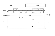
可能な改良の断面図を図7に示す。
ここでは、キャパシタ及びスイッチは、金属製の光シールド124を備えたMOS構造として実現されている。かかるシールドは、キャパシタ領域上に堆積され、誘電体は金属シールド124とスイッチ121、120及びキャパシタ122の金属又はポリシリコンゲートとの間に配置される。増幅及び増殖回路は図示されていない。
【0048】
低い暗電流を備えたピクセルを得るためのウエルピクセルの適用
フォトダイオードの暗電流がダイオードのエッジ又はシリコンとSiO2との界面における熱的発生メカニズムによることはよく知られている。CCDの暗電流は、インバージョンモード又はオールフェースピンニングと呼ばれる方法により十分に低減されている。このようなCCDにおいて、Si−SiO2界面は反転させられ、埋め込みチャネル(有用な検知体積)はこの界面とはコンタクトを有しない。かかる方法は典型的には100のファクターで暗電流を減少することができる。
【0049】
本発明のウエルピクセルは、同じ目的のために適用される。もしピクセルが光コレクション接合に対して大きければ、他の領域はその材料のバルクを表面からさえぎる構造により覆われる。これには2つの方法がある。
(A)スクリーンジャンクション32の使用
(B)反転層132の使用これはポリシリコンゲート電極により引き起こされる。
【0050】
(A)の例を図8に示す。
(B)の2つの例は図9示される。ここにおいて、バリア領域中のスクリーニング反転層132を形成するポリシリコンゲート電極37が示されている。
【0051】
CCD又はCCD類似の構造における改良
本発明は、能動又は受動ピクセル構造に対しても適用可能であり、図10に示すようなCCD構造に対しても適用できる。本発明の光コレクション接合は、フォトダイオードからなるが、半導体基板45に対する空乏層又は反転層41からなる接合であってもよい(表面チャネルCCDのように)。また、本発明の光コレクション接合は、半導体基板に埋め込まれた(部分的に)空乏層された埋め込みチャネルによっても形成することができる(埋め込みチャネルCCDのように)。
【0052】
かかる構造は、典型的にはCCD、CID(チャージインゼクションデバイス)、フォトゲート、又はそれらにおいて用いられる。これらはバーチャル接合と呼ばれ、光生成電荷キャリアを集める物理的なnp接続と同じような機能を実際に有する。CCDセルはこのようにそれ自体光検知エレメントであり、CCDエレメント49により電気静電誘導されたポテンシャルポケットに蓄えられる。もしポテンシャルバリアが光センシティブ体積(基板47)とポテンシャルポケットとの間に存在した場合、電荷の収集が妨げられるであろう。
【0053】
本発明は、このようにバーチャルジャンクションの電荷収集の増加にも用いることができる。図10においては、CCD類似の構造の表面チャネルの断面図が示されている。ここにおいて、CCDの反転層41に到達する基板からの電子のためのバリアが供給される。
(A)pウエル43の開口により(省略)。
(B)そのポテンシャルバリアを貫き又は低くする本発明の原理に基づく明白なn型注入44による。
【図面の簡単な説明】
【図1】 (A)(B)は、本発明の第1及び第2の具体例の検知器の概略図である。
【図2】 図1(A)のラインIに沿った断面における検知器の電気ポテンシャルを示す。
【図3】 図1(A)のラインIIに沿った断面における電気ポテンシャルを示す。
【図4】 モンテ・カルロ・シミュレーションによる図1(A)の構造における電荷キャリアの拡散シミュレーションを示す。
【図5】 (A)(B)は、本発明(5(B))及び従来技術(5(A))に基づいて製造された検知器の測定結果を示す。
【図6】 ピクセル上にメモリエレメントを備えた本発明のピクセル構造を示す。
【図7】 図6のピクセル構造の可能な改良を施した半導体基板の断面図を示す。
【図8】 第1の低い暗電流ピクセルの本発明の検知器を示します。
【図9】 第2の暗電流ピクセルに適用した本発明の検知器の構造を示す。
【図10】 本発明の原理による表面チャネルCCD類似構造の断面図を示す。
【符号の説明】
1 第1の領域、2 第2の領域、3 p+領域、4 第4領域、5 p−層、6 半導体基板。[0001]
BACKGROUND OF THE INVENTION
The present invention relates to the field of semiconductor-based detectors for electromagnetic radiation. Furthermore, it relates to a semiconductor detector and a semiconductor pixel structure with a wide radiation detection area or a high fill factor.
The invention also relates to a method for manufacturing such a detector.
[0002]
[Prior art]
Semiconductor-based sensors and devices that detect electromagnetic radiation are well known. For example, a sensor as described in EP-A-739039 and WO93 / 19489. These sensors are formed by CMOS or MOS technology. In those sensors, the region added to collect the charge carriers generated by radiation in the semiconductor substrate is formed from a pn or np junction, and the substrate is an n-type conductor or p-type conductor, respectively. Formed from the body. Such a junction is called a connection junction. In image sensors formed using CMOS or MOS technology, a CMOS or MOS image sensor with a passive pixel is distinguished from a CMOS or MOS image sensor with an active pixel. The sensor of EP-A-739039 or WO 93/19489 is an active pixel sensor.
[0003]
[Problems to be solved by the invention]
An active pixel sensor is formed with a pixel integrated means for charge amplification, such charge being collected by a light sensitive element or configuration in the pixel. Passive pixels do not have such means and require a charge sensitive amplifier, which is not integrated into the pixel and is connected to the pixel by long wires. Due to the additional electrical components of the active pixel, the active pixel image sensor can be formed to perform more sophisticated functions and can be superior in the performance of the imaging device or system based on the sensor. Such functions can include filtering, high speed operation, or operation in higher illumination conditions.
However, active pixel CMOS or MOS image sensors have significant drawbacks. Such drawbacks are less, but also present in passive pixel sensors. That is, an important part of the surface of the pixel is used in the readout circuit.
[0004]
It is well known that the charge sensing volume (Volume) of a pn or np junction is wider than the depletion layer of such a junction. In fact, all charges generated within the range called recombination length from the collection junction have the opportunity to diffuse and collect at such junction. Based on this mechanism, it is possible to form a sensor with a small junction and a wide light sensing volume. The optical sensor can comprise a 3 × 2 μm junction and a 15 μm recombination length. Thus, in appearance, such a detector has a surface size or light detection area with a diameter of 30 μm.
However, if an irrelevant electrical circuit, such as a lead-out circuit, is provided adjacent to such a collection junction, some of the charge to reach the collection junction is due to the junction or structure of the readout circuit. Collected. The charge carriers generated by the light poured onto the area of the detector used in the readout circuit from there are mainly collected by the junction of such readout circuit. The area taken up by the readout circuit in the pixel impairs collecting radiation, which causes a low fill factor or low sensitivity of the sensor-based active pixel.
[0005]
The book "Solid-State Imaging with Charge Coupled Devises, A. THEUwiwissen (Kluwer Academic publishers, 1995 ISDN 0-7923-3456-6)" outlines the current state of image devices based on semiconductors. This is the case with CCD and MOS cameras, for example. Chapter 7 of this book discusses topics that increase pixel fill factor or sensitivity. Such a method is based on the use of a microlens or a light conversion top layer.
[0006]
Figure 4 of the paper “NyW detector a smart two-dimensional particle detector, Bart Dierckx” (Nuclear Instruments and Methods in Physics Research, vol. A275 (1989), p.542-544) shows a pixel device based on a semiconductor. Four forming methods are described. The first method is based on the classic CMOS process. The disadvantage of this method is the low fill factor because the readout electrical circuit covers a portion of the semiconductor surface. In other methods proposed to solve such a fill factor problem, an uncommon CMOS technology is used to solve the problem. That is, flip chip (bump bonding), SOI (silicon-on-insulator) technology, or a technology for moving the photon detection zone onto the amorphous top layer.
[0007]
Figure 2 of the paper “Design and Performance of semiconductor detectors with integrated amplification and charge storage capability, P. Klein & al” (Nuclear Instruments and Methods in Physics Research, vol. A305 (1991), p. 517-526) A semiconductor-based sensor using a transistor junction is shown. Here, the charge generated in the semiconductor substrate is prevented from diffusing into the source and drain junctions of the transistor by the junction-based barrier and is forced into the gate. Such a gate is in contact with the source and drain.
[0008]
Avalanche photodiodes (APDs) are more known. The APD has a p ++ / p− / p ++ / n ++ continuous layer structure, where the p ++ layer is a back contact, the p− layer is a sensing layer, the p + layer is a layer for providing avalanche amplification of electrons, and an n ++ layer Is the layer that finally collects the propagated electrons. The doping amount and width of such a propagation layer is very strict. Furthermore, the voltage applied to such a structure is quite high and is close to the electrical breakdown of such a structure. The junction of the p− / p + layer does not act as a barrier for electron diffusion but acts as an avalanche amplification device.
[0009]
Accordingly, the present invention is a semiconductor device for detecting electromagnetic radiation, in which all charge carriers formed by radiation in the semiconductor are collected in a collecting junction or region and collected in a junction or region of a readout circuit. The purpose is to provide no structure.
[0010]
[Means for Solving the Problems]
The present invention relates first to a detector for electromagnetic radiation including a semiconductor substrate, the substrate including first and second regions. The first region and the second region are attached to collect charge carriers formed by radiation in the substrate. The substrate further includes a third region that forms a barrier that can sufficiently prevent the diffusion of charges to the second region.
Between the substrate and such a first region, there is no barrier, there is an almost zero barrier, or there is a barrier that is sufficiently lower than the barrier between the second region and the substrate.
The third region can also form a sufficiently low barrier for such charge carriers to diffuse into the first region.
[0011]
Furthermore, the invention relates to a radiation detector with a small but effective barrier between the radiation detection volume in the semiconductor substrate and the region or junction with the readout circuit. Such detectors have no or low barriers between the radiation detection volume in the semiconductor and the regions and junctions added to collect the charge carriers formed by the radiation. .
[0012]
According to a first aspect of the invention, some portion of the charge carriers generated by the substrate adjacent to and particularly below the second region is collected by such first region. The substrate has a first conductivity type dopant, and the first region and the second region have another second conductivity type dopant. The third region has the first conductivity type, and the doping amount of the third region is higher than the doping amount of the substrate.
[0013]
According to a second aspect of the present invention, the first region forms a bond with the substrate, and the second region forms a bond with the third region.
[0014]
In addition, according to another aspect of the present invention, a MOS-based pixel structure for detecting light including the detector of the present invention is described. In this case, the third region forms an electrical barrier sufficient to prevent electrons or holes from diffusing into the second region. Such an electrical barrier can be formed at the interface between the third region and the substrate.
A sufficiently low electrical barrier is formed at the interface between the first region and the substrate for electrons or holes to diffuse from the substrate to the first region. The second region is the portion of the circuit for processing the signal generated by the charge carriers in the first region. Such a signal is a current generated in the first region. The pixel structure may further include such a first region and a fourth region adjacent to the substrate. A sufficiently low barrier is formed at the interface of the substrate between the fourth region and the substrate.
[0015]
According to another aspect of the present invention, a method for manufacturing and operating a CMOS pixel structure for detecting electromagnetic radiation is described.
[0016]
The present invention further includes the design integration principle of the invention of the CMOS pixel structure and sensor and of the invention of the CCD or CCD-like structure. The present invention has significant advantages for application to low noise light detection.
[0017]
DETAILED DESCRIPTION OF THE INVENTION
The present invention relates to a detector or semiconductor detector with a small but effective barrier between a radiation detection volume in a semiconductor substrate and a region and junction with a readout circuit.
The invention also relates to a detector with a nonexistent or very low barrier between the radiation detection volume in the semiconductor and the regions and connections provided to collect the charge carriers generated by the radiation. is there. The region that forms a barrier between the radiation detection volume where the charge is generated and the electrical part not having the extraction circuit relationship can comprise a dopant of the same conductivity type as the radiation detection volume.
[0018]
The detector of the present invention is comprised of a collection junction and other electrical parts that collect the charge carriers generated by radiation. Such collection junctions enhance the collection of charge carriers formed in the radiation sensing volume adjacent to the bottom of such other electrical configurations. Such a function is formed by an electrical barrier means formed at the interface with a region having the same conductivity type as such a volume below the other electrical components. Such a barrier prevents charge carriers formed below the other electrical component from diffusing into the junction or structure of the other electrical component. This electrical barrier is not present below the collection junction or is sufficiently low. As a result, charge carriers generated under other electrical components are collected.
[0019]
Such a detector is realized by a CMOS process, the configuration is made of a p-type substrate, and the region forming the electrical barrier is realized as a p + type implant. Other components are formed including various conductivity types, i.e., n-type junctions. The collection junction is formed from an n-type region with a low electrical barrier to the substrate. The area of the barrier that is lower or not formed coincides with, partially or completely coincides with or consists of a collection junction. A low or nonexistent barrier can be achieved by adding an n-type implant to the area of the collection junction. Alternatively, it can be realized by not performing p + type implantation that realizes the electrical barrier.
Such p + type implantation is called p-well implantation, is called anti-punch-through implantation, is called blanket implantation, or is called Vth adjustment implantation. These have almost the same effect in the CMOS process and are often useful as standard processes in the CMOS process.
[0020]
Such n-type implantation is called n-well implantation, is called anti-punch-through implantation, is called blanket implantation, or is called Vth adjustment implantation.
[0021]
In an alternative embodiment of the present invention, a detector that forms part of a pixel structure with a collection junction that does not perform deeper n-type implantation or formation of a p + p-barrier comprises a MOSFET having one electrode ( Source or drain). The other electrodes are kept at a constant voltage. The exact voltage is not appropriate. That is, the other electrodes may not be floating nodes. The collection junction is preferably completely or partially surrounded by the gate of the MOSFET. The other electrode completely or partially surrounds the gate and the first electrode. The gate of the MOSFET is biased off and both electrodes are electrically isolated. The MOSFET gate and other electrodes surrounding the junction reduce the portion of dark current due to the junction edge effect.
[0022]
The principle of the present invention can be applied to a CCD or a CCD-like structure (photogate, charge injection device (CID), charge sweep device (CSD)), in which the collecting junction is an inversion layer. Or it consists of a buried channel under the CCD electrode. That is, a surface channel CCD or a buried channel CCD. It is also possible to replace the collection junction or part thereof with such a structure.
[0023]
In the method described in the present invention, the present invention will eventually be described by means such as a CMOS photosensor with a pixel structure as described in EP-A-0739039. EP-A-0739039 is hereby attached as an attached document.
Eventually, as stated by way of example, the semiconductor substrate is assumed to be a p-type conductor. However, it is easy for those skilled in the art to imagine an n-type conductive semiconductor substrate from such description. Other equivalent embodiments will be apparent to those skilled in the art, and the spirit and scope of the invention are not limited to the language of the appended claims.
[0024]
FIG. 1A shows part of a pixel structure comprising a
[0025]
In the p +
[0026]
Furthermore, in addition, it is also possible to form the n-type
[0027]
FIG. 1B illustrates another specific example of the structure illustrated in FIG.
2 and 3 show electrical potentials in cross sections taken along the first and second sides of the structure shown in FIG.
The structure shown in FIG. 1 has a partial potential minimum in the p-region, as shown in FIGS. As shown in FIG. 2, the electrons in the p− region do not easily diffuse into the
[0028]
In the matrix of pixels according to the invention, it is simulated that the electrons generated by the radiation work randomly. The pixel is formed based on the structure shown in FIG. The average electron diffusion distance is recorded. The diffusion distance in the structure in which the
[0029]
[Table 1]
The resulting diffusion distance is close to the ideal result (3.75 μm). This type of pixel thus has a near ideal modulation transfer function (MTF). It has a fill factor of almost 100%, which means that all surfaces of the pixel matrix that are exposed to light contribute to the collection of light.
All of the substrate charge carriers actually generated by the light flow to the collection junction. In the prior art pixel structure, some of the generated charge carriers are collected by the connection of the extraction circuit and such charges disappear.
[0031]
The introduction of
(1) An optical trap inside the drawer circuit, its own connection. This is certainly a limitation for short wavelengths and has a low penetration depth.
(2) Reflection of light by the joint metal.
(3) Recombination. Free electrons do not diffuse indefinitely and recombine after a certain typical recombination length. In CMOS technology, this length exceeds several times the pixel pitch.
[0032]
The second is image sharpness or MTF. In the case where the
[0033]
Preferred embodiments of the invention
In a standard CMOS process, two small arrays of photodiodes (A, B) are formed as part of an integrated circuit. In the case of (A), the junction consists of a shallow n-type region in a p-type substrate as in the prior art. The junction size is 2 × 2 μm and the pixel pitch is 7.5 μm. The central column of the pixel array is exposed to light and adjacent columns of pixels are shielded from light by a metal shield. The parallel output of the pixel column is provided external to the integrated circuit so that the effective photocurrent of the pixel column can be measured.
[0034]
In the case of (B), the substrate is identical to the above structure except that a small 2 × 2 μm n-well implant is formed inside the photodiode in all photodiodes. The CMOS process used here is called a p-well, which is supplementarily provided in the n-well. Other areas that are not exposed to the n-well implant are implanted with p-type dopant so that the p-type node is close to the surface in such areas.
[0035]
The final structure is preferably a specific example of a detector according to the schematic diagram of the invention shown in FIG. In an ideal case, the exposed column of pixels senses all photocurrent, and the covered column of pixels is preferably zero current. This is a case where lateral charge diffusion and light reflection do not occur.
[0036]
The measurement results are summarized in FIG. 5, where A is the case of the prior art and B is the case with regions and junctions according to the present invention. In the results shown in FIG. 5, A1 / B1 is the current collected by the exposed pixel, A2 / B2 is the current collected by the covered adjacent pixel, and A3 / B3 is further adjacent to the pixel. A4 / B4 is the current layer of four pixels adjacent to such a pixel in succession.
The change in behavior due to the effect of the n-well dot as shown in FIG. 5B shows the principle of the present invention. Not only does the exposed central pixel column collect more photocurrent (B1), but the absolute amount of total current is much higher, which also causes structure B to lose current due to charge carrier recombination in structure A. Indicates that they are collecting.
[0037]
Other implementations of many types of active pixels also show many excellent differences. In the preferred embodiment, we use a three transistor pixel structure as shown in EP-A-0739039. The addition of a small dot in the n-well inside the photodiode increases the collected current sharply, 5 to 10 times for 650 nm light. Considering the fact that the pixels are formed with a 15% fill factor (exposed photodiode only area), a factor of 5 to 10 indicates that the fill factor is close to 100%.
[0038]
The advantages of the detector of the present invention are further as follows.
Photo charge generated by light incident on the pixel area not covered by the photodiode junction is collected by the photodiode connection. This is even if this area is covered by a drawer circuit that includes connections that can collect photogenerated charges. The pixel of the present invention has a fill factor close to 100%, except for portions that are covered by an opaque material such as a metal bond. Charges generated within unrelated circuit connections are lost for detection. These connections are shallow, and radiation with a wavelength of about 500 to 600 nm or less is converted into electron hole pairs deep in the silicon substrate, and this effect only causes a slight decrease in detection performance.
[0039]
The capacity of the collection junction of the detector of the present invention is very small compared to the capacity of the connection that covers the entire pixel surface, so that they effectively have a similar light collecting surface. One of the main noise sources of imaging sensors is what is called KTC noise. This noise is typically expressed as a measure of the deterministic noise charge of the photocharge measurement and is proportional to the square root of the junction capacitance. In order to obtain a pixel with a low noise charge, a low-capacitance photodiode must be designed. For a given capacity for a unit area, the lowest noise diode has the narrowest area, i.e. the low light collection area. The present invention forms a photodiode with a small connection area and a small connection capacitance, but with a large collection volume.
[0040]
The device of the preferred embodiment of the present invention is satisfied by having an implant applied in general CMOS technology. Thereby, a necessary profile can be realized. The structure of the present invention can also be obtained in standard CMOS technology. It is a foundry with the characteristics in the CMOS process called twin well. Other foundries have similar structures but are called differently. That is, anti-punch through injection, blanket injection, Vth adjustment injection, and the like. The principle itself is the same and can be used in the same way as a method of realizing the preferred embodiment of the present invention. In a twin well CMOS process, both nMOS and pMOS structures are formed in their own wells (formed in p and n wells, respectively). As a result, the silicon substrate becomes a lightly doped p-type, or consists of a lightly doped p-type crystal growth layer formed on a highly doped wafer.
[0041]
The pMOS structure is formed in the n-well and is deeply connected to the substrate. The nMOS structure is formed in the p-well and in this case is not connected. (This is because such p-type is the same type as the substrate type). However, an nMOS structure is formed in a portion that is more highly doped than the underlying substrate. This is similar to the structure introduced to form short channel transistors in a standard CMOS process. The present invention is realized by using an n-junction as an optical collecting correction junction, and is realized through a p + / p− barrier by covering an n-junction portion accompanied by an n-well injection.
[0042]
The n-well implant is deep and penetrates through the p-well into the lightly doped substrate. As a result, other nMOSFETs that are part of the active or passive pixel are formed with only shallow junctions and do not reach the substrate. If the complexity of the active pixel requires that a pMOSFET be included, i.e., it needs to be formed in an n-well, this n-well, i.e. an n-well that is the same type of connection as the optical collecting junction, It should be noted that this would be comparable to an optical collecting junction and an optical collecting connection and would cancel some of its effects.
[0043]
This problem does not occur in active pixels using only one type of MOSFET. In normal processes, this situation can be mitigated by having a deep p-type implant in the n-well beyond the pMOSFET, not because of the light collection junction.
Junction spikes are known as the effect of metallization spikes through shallow junctions. This is one of the causes of high dark current pixels. By placing critical diodes in contact over the possible wells of the pixel of the present invention, substrate leakage can be avoided. This occurs beyond the small number of white pixels in the pixel matrix.
[0044]
Other embodiments of the invention
The photo-collecting connection of the pixels of the CMOS sensor according to the invention can also be formed from a MOS structure or an inversion region or a cavity region of a buried channel MOSFET.
The optical collecting connection may be a phototransistor, which can be formed from a vertical pnp structure, in which the collector is a substrate, the base is a deep n-well injection layer, and the emitter is This is a p-type region that forms a shallow connection inside the well. Such a structure has charge collecting characteristics as in the preferred embodiment of the present invention, but also includes the added value of internal current multiplication.
[0045]
Pixel with integrated memory element
The present invention can also form pixels with memory elements in the pixels, such memory elements being better shielded from light. An analog memory element is usually a capacitor, which is part of a junction or a connection to other circuit elements such as a transistor having a junction.
The connection senses light, and such light sensing characteristics cause a current flow that affects the charge stored in the capacitor. Memory elements or capacitors can be used for various purposes. For example, storage of spatial and temporal exudation images.
FIG. 6 shows an example of a frame circuit with a slow integration time, which can be read at high speed in a non-destructive manner. In this figure, the light collection junction (1, 4-5, 6) is reset by a switch (eg, MOSFET 20).
[0046]
The signal obtained by the light collection junction is periodically sampled by the
However,
If the photodiode (1, 4-5, 6) is formed in accordance with the present invention, the charge diffusing in the substrate is collected in the photodiode (1, 4-5, 6) and the charge on the
[0047]
A cross-sectional view of a possible improvement is shown in FIG.
Here, the capacitor and the switch are realized as a MOS structure including a
[0048]
Application of well pixels to obtain pixels with low dark current
The dark current of the photodiode is the edge of the diode or silicon and SiO 2 It is well known that this is due to the thermal generation mechanism at the interface. The dark current of the CCD is sufficiently reduced by a method called inversion mode or all-face pinning. In such a CCD, Si-SiO 2 The interface is reversed and the buried channel (useful sensing volume) has no contact with this interface. Such a method can typically reduce dark current by a factor of 100.
[0049]
The well pixel of the present invention is applied for the same purpose. If the pixel is large relative to the light collection junction, other areas are covered by structures that block the bulk of the material from the surface. There are two ways to do this.
(A) Use of
(B) Use of
[0050]
An example of (A) is shown in FIG.
Two examples of (B) are shown in FIG. Here, the
[0051]
Improvement in CCD or CCD-like structure
The present invention can be applied to an active or passive pixel structure, and can also be applied to a CCD structure as shown in FIG. The light collection junction of the present invention is made of a photodiode, but may be a junction made of a depletion layer or an
[0052]
Such structures are typically used in CCDs, CIDs (charge injection devices), photogates, or the like. These are called virtual junctions and actually have a function similar to a physical np connection that collects photogenerated charge carriers. The CCD cell is thus a light sensing element itself and is stored in a potential pocket that is electrically electrostatically induced by the
[0053]
The present invention can thus also be used to increase the charge collection of virtual junctions. In FIG. 10, a cross-sectional view of a surface channel having a structure similar to a CCD is shown. Here, a barrier for electrons from the substrate reaching the
(A) By opening the p-well 43 (omitted).
(B) By an obvious n-
[Brief description of the drawings]
FIGS. 1A and 1B are schematic views of detectors according to first and second specific examples of the present invention. FIGS.
FIG. 2 shows the electrical potential of the detector in a cross section along line I in FIG.
FIG. 3 shows an electric potential in a cross section taken along line II in FIG.
FIG. 4 shows a charge carrier diffusion simulation in the structure of FIG. 1A by Monte Carlo simulation.
5A and 5B show the measurement results of a detector manufactured based on the present invention (5 (B)) and the prior art (5 (A)).
FIG. 6 shows the pixel structure of the present invention with memory elements on the pixel.
7 shows a cross-sectional view of a semiconductor substrate with possible improvements of the pixel structure of FIG.
FIG. 8 shows the inventive detector of the first low dark current pixel.
FIG. 9 shows the structure of the detector of the present invention applied to a second dark current pixel.
FIG. 10 illustrates a cross-sectional view of a surface channel CCD-like structure according to the principles of the present invention.
[Explanation of symbols]
DESCRIPTION OF
Claims (23)
前記第1の層の上に配置された、第3のドーパント濃度を持つ前記第1の導電型の第2の層と、
実質的に前記第2の層の内部に配置された、第4のドーパント濃度を持つ第2の導電型の第1の領域と第2の領域と、
を備えてなり、
前記第2の層が、前記第1の領域と前記第2の領域とを分離し、かつ、前記第1および第2の領域と前記第1の層とを分離する第3の領域を有し、
前記第3の領域が、前記第1の層から前記第2の領域への電荷キャリアの拡散に対するバリアを有し、
さらに、
第5のドーパント濃度を持つ前記第2の導電型の第4の領域であって、前記第1の領域から前記第3の領域を通って前記第1の層内に延在する第4の領域において、前記第1の領域が、前記電荷キャリアを収集するための収集接合を有する第4の領域と、
を備えてなる電磁放射検出器。A first conductivity type semiconductor substrate having a first dopant concentration, a semiconductor substrate having a defined in its substrate, a first layer of said first conductivity type having a second dopant concentration When,
A second layer of the first conductivity type disposed on the first layer and having a third dopant concentration;
A first region and a second region of a second conductivity type having a fourth dopant concentration, disposed substantially within the second layer ;
With
The second layer has a third region that separates the first region and the second region and separates the first and second regions from the first layer. ,
Said third region, have a barrier to diffusion of charge carriers into said first from said layer of the second region,
further,
A fourth region of the second conductivity type having a fifth dopant concentration and extending from the first region through the third region into the first layer; The first region has a fourth region having a collection junction for collecting the charge carriers ;
An electromagnetic radiation detector comprising:
前記p-層中の上にp+層を定めて、前記p型基板および前記p-層内に発生する光電荷に対する拡散バリアを設けるステップと、
実質的に前記p+層内に、第1のn++領域および第2のn++領域を定めるステップであって、前記第1のn++領域が、前記p+層によって、前記第2のn++領域及び前記p-層から分離され、そして、前記第2のn++領域が、前記p+層によって、前記第1のn++領域および前記p-層から分離されるステップと、
前記p型基板および前記p-層内に発生する前記光電荷を前記第1のn++領域に収集するための、前記第1のn++領域および前記p+層を通って前記p-層内に至るn型領域を定めるステップと、を、
含んでなる、電磁放射線検出用のCMOSベースのピクセル構造の製造方法。defining a p - layer in a p-type substrate;
A step of providing a diffusion barrier to light charge generated in the layer, - the p - defines the p + layer over the layer, the p-type substrate and the p
Substantially the p + layer in comprising the steps of: defining a first n ++ region and a second n ++ region, the first n ++ region is, by the p + layer, the second Two n ++ regions and the p − layer, and the second n ++ region is separated from the first n ++ region and the p − layer by the p + layer. Steps,
The p-type substrate and the p - said through for collecting the light charge generated in the layer on the first n ++ region and said first n ++ region and the p + layer p - Defining an n-type region into the layer;
A method for manufacturing a CMOS-based pixel structure for electromagnetic radiation detection.
前記n-層中の上にn+層を定めて、前記n型基板および前記n-層内に発生する光電荷に対する拡散バリアを設けるステップと、
実質的に前記n+層内に、第1のp++領域および第2のp++領域を定めるステップであって、前記第1のp++領域が、前記n+層によって、前記第2のp++領域および前記n-層から分離され、そして、前記第2のp++領域が、前記n+層によって、前記第1のp++領域および前記n-層から分離されるステップと、
前記n型基板および前記n-層内に発生する前記光電荷を前記第1のp++領域に収集するための、前記第1のp++領域および前記n+層を通って前記n-層内に至るp型領域を定めるステップと、を、
含んでなる、電磁放射線検出用のCMOSベースのピクセル構造の製造方法。defining an n − layer in an n-type substrate;
A step of providing a diffusion barrier to light charge generated in the layer, - the n - defines the n + layer on the top in the layer, the n-type substrate and the n
Substantially the n + layer in comprising the steps of: defining a first p ++ region and a second p ++ region, the first p ++ regions, by the n + layer, the second Two p ++ regions and the n − layer, and the second p ++ region is separated from the first p ++ region and the n − layer by the n + layer. Steps,
The n-type substrate and the n - wherein said light charge generated in the layer for collecting the first p ++ regions, through the first p ++ region and the n + layer n - Defining a p-type region leading into the layer;
A method for manufacturing a CMOS-based pixel structure for electromagnetic radiation detection.
Applications Claiming Priority (4)
| Application Number | Priority Date | Filing Date | Title |
|---|---|---|---|
| US3753197P | 1997-02-10 | 1997-02-10 | |
| EP97870084A EP0883187A1 (en) | 1997-06-04 | 1997-06-04 | A detector for electromagnetic radiation, pixel structure with high sensitivity using such detector and method of manufacturing such detector |
| BE60/037531 | 1997-10-24 | ||
| BE97870084-7 | 1997-10-24 |
Publications (2)
| Publication Number | Publication Date |
|---|---|
| JPH1131839A JPH1131839A (en) | 1999-02-02 |
| JP4053651B2 true JP4053651B2 (en) | 2008-02-27 |
Family
ID=26148244
Family Applications (1)
| Application Number | Title | Priority Date | Filing Date |
|---|---|---|---|
| JP06757598A Expired - Lifetime JP4053651B2 (en) | 1997-02-10 | 1998-02-09 | Electromagnetic radiation detector, high-sensitivity pixel structure using the detector, and method of manufacturing the detector |
Country Status (5)
| Country | Link |
|---|---|
| EP (1) | EP0858111B1 (en) |
| JP (1) | JP4053651B2 (en) |
| KR (1) | KR100545801B1 (en) |
| AT (1) | ATE473520T1 (en) |
| DE (1) | DE69841754D1 (en) |
Families Citing this family (14)
| Publication number | Priority date | Publication date | Assignee | Title |
|---|---|---|---|---|
| US6815791B1 (en) | 1997-02-10 | 2004-11-09 | Fillfactory | Buried, fully depletable, high fill factor photodiodes |
| US7106373B1 (en) | 1998-02-09 | 2006-09-12 | Cypress Semiconductor Corporation (Belgium) Bvba | Method for increasing dynamic range of a pixel by multiple incomplete reset |
| US8063963B2 (en) | 1998-02-09 | 2011-11-22 | On Semiconductor Image Sensor | Imaging device having a pixel structure with high dynamic range read-out signal |
| EP1109229A3 (en) * | 1999-12-14 | 2008-03-26 | Fillfactory N.V. | Buried, fully depletable, high fill factor photodiodes |
| WO2004099740A2 (en) * | 2003-05-08 | 2004-11-18 | Council For The Central Laboratory Of The Research Councils | Accelerated particle and high energy radiation sensor |
| ES2298485T3 (en) | 2003-11-21 | 2008-05-16 | Carestream Health, Inc. | DENTAL RADIOLOGY DEVICE. |
| WO2006056086A1 (en) * | 2004-11-25 | 2006-06-01 | Waeny Martin | Optoelectronic sensor having high dynamics and a low offset noise |
| US7808022B1 (en) | 2005-03-28 | 2010-10-05 | Cypress Semiconductor Corporation | Cross talk reduction |
| US7750958B1 (en) | 2005-03-28 | 2010-07-06 | Cypress Semiconductor Corporation | Pixel structure |
| JP5387212B2 (en) * | 2009-07-31 | 2014-01-15 | 富士通セミコンダクター株式会社 | Semiconductor device and manufacturing method thereof |
| KR101304094B1 (en) * | 2012-05-23 | 2013-09-05 | 서울대학교산학협력단 | Device of scanning electromagnetic wave using structure of flash memory and method thereof |
| JP6381135B2 (en) * | 2015-04-21 | 2018-08-29 | マイクロシグナル株式会社 | Photoelectric conversion element |
| JP2018156984A (en) * | 2017-03-15 | 2018-10-04 | 株式会社東芝 | Photo detection element |
| JP2022039524A (en) * | 2020-08-28 | 2022-03-10 | 株式会社東芝 | Semiconductor device |
Family Cites Families (5)
| Publication number | Priority date | Publication date | Assignee | Title |
|---|---|---|---|---|
| JPS57193073A (en) * | 1981-05-22 | 1982-11-27 | Fuji Electric Co Ltd | Semiconductor radioactive ray detector |
| JPS57201085A (en) * | 1981-06-03 | 1982-12-09 | Fuji Electric Corp Res & Dev Ltd | Semiconductor radiation detector |
| DE4209536C3 (en) * | 1992-03-24 | 2000-10-05 | Stuttgart Mikroelektronik | Image cell for an image sensor chip |
| EP0739039A3 (en) * | 1995-04-18 | 1998-03-04 | Interuniversitair Micro-Elektronica Centrum Vzw | Pixel structure, image sensor using such pixel, structure and corresponding peripheric circuitry |
| US5614744A (en) * | 1995-08-04 | 1997-03-25 | National Semiconductor Corporation | CMOS-based, low leakage active pixel array with anti-blooming isolation |
-
1998
- 1998-02-06 AT AT98870025T patent/ATE473520T1/en not_active IP Right Cessation
- 1998-02-06 DE DE69841754T patent/DE69841754D1/en not_active Expired - Lifetime
- 1998-02-06 EP EP98870025A patent/EP0858111B1/en not_active Expired - Lifetime
- 1998-02-09 KR KR1019980003639A patent/KR100545801B1/en not_active IP Right Cessation
- 1998-02-09 JP JP06757598A patent/JP4053651B2/en not_active Expired - Lifetime
Also Published As
| Publication number | Publication date |
|---|---|
| ATE473520T1 (en) | 2010-07-15 |
| DE69841754D1 (en) | 2010-08-19 |
| KR19980071190A (en) | 1998-10-26 |
| JPH1131839A (en) | 1999-02-02 |
| KR100545801B1 (en) | 2006-04-21 |
| EP0858111B1 (en) | 2010-07-07 |
| EP0858111A1 (en) | 1998-08-12 |
Similar Documents
| Publication | Publication Date | Title |
|---|---|---|
| US6225670B1 (en) | Detector for electromagnetic radiation, pixel structure with high sensitivity using such detector and method of manufacturing such detector | |
| US7253019B2 (en) | Buried, fully depletable, high fill factor photodiodes | |
| KR100262774B1 (en) | Top bus virtual phase frame interline transfer ccd image sensor | |
| US6388243B1 (en) | Active pixel sensor with fully-depleted buried photoreceptor | |
| JP3702854B2 (en) | Solid-state image sensor | |
| US9165972B2 (en) | Semiconductor structure, method of operating same, and production method | |
| BE1022430B1 (en) | A PIXEL STRUCTURE | |
| US6982183B2 (en) | Method and system for manufacturing a pixel image sensor | |
| KR100879013B1 (en) | Phototransistor having a buried collector | |
| US5306931A (en) | CCD image sensor with improved antiblooming characteristics | |
| US20070145503A1 (en) | Pixel structure with improved charge transfer | |
| TWI382531B (en) | Photodetector and n-layer structure for improved collection | |
| JP4053651B2 (en) | Electromagnetic radiation detector, high-sensitivity pixel structure using the detector, and method of manufacturing the detector | |
| JP3009730B2 (en) | Anti-blooming structure for solid-state image sensor | |
| CA2577198A1 (en) | Semiconductor radiation detector with a modified internal gate structure | |
| US6150704A (en) | Photoelectric conversion apparatus and image sensor | |
| JP3125303B2 (en) | Solid-state imaging device | |
| US20070069260A1 (en) | Photodetector structure for improved collection efficiency | |
| KR101373866B1 (en) | Two epitaxial layers with buried subcollector to reduce crosstalk in an image sensor | |
| Dierickx et al. | Near-100% fill factor standard CMOS active pixel | |
| GB2387270A (en) | Method to increase the conversion gain of an active pixel | |
| JP5145528B2 (en) | Shielded CMOS pixel structure with dual purpose electrode | |
| JP4250857B2 (en) | Solid-state image sensor | |
| JP2002289827A (en) | Solid-state imaging device and manufacturing method therefor |
Legal Events
| Date | Code | Title | Description |
|---|---|---|---|
| A711 | Notification of change in applicant |
Free format text: JAPANESE INTERMEDIATE CODE: A711 Effective date: 20040219 |
|
| A521 | Request for written amendment filed |
Free format text: JAPANESE INTERMEDIATE CODE: A821 Effective date: 20040219 |
|
| A621 | Written request for application examination |
Free format text: JAPANESE INTERMEDIATE CODE: A621 Effective date: 20040319 |
|
| A977 | Report on retrieval |
Free format text: JAPANESE INTERMEDIATE CODE: A971007 Effective date: 20060306 |
|
| A131 | Notification of reasons for refusal |
Free format text: JAPANESE INTERMEDIATE CODE: A131 Effective date: 20060502 |
|
| A601 | Written request for extension of time |
Free format text: JAPANESE INTERMEDIATE CODE: A601 Effective date: 20060801 |
|
| A602 | Written permission of extension of time |
Free format text: JAPANESE INTERMEDIATE CODE: A602 Effective date: 20060804 |
|
| A711 | Notification of change in applicant |
Free format text: JAPANESE INTERMEDIATE CODE: A711 Effective date: 20061027 |
|
| A521 | Request for written amendment filed |
Free format text: JAPANESE INTERMEDIATE CODE: A523 Effective date: 20061102 |
|
| A521 | Request for written amendment filed |
Free format text: JAPANESE INTERMEDIATE CODE: A821 Effective date: 20061027 |
|
| RD02 | Notification of acceptance of power of attorney |
Free format text: JAPANESE INTERMEDIATE CODE: A7422 Effective date: 20070125 |
|
| RD03 | Notification of appointment of power of attorney |
Free format text: JAPANESE INTERMEDIATE CODE: A7423 Effective date: 20070125 |
|
| RD04 | Notification of resignation of power of attorney |
Free format text: JAPANESE INTERMEDIATE CODE: A7424 Effective date: 20070208 |
|
| A131 | Notification of reasons for refusal |
Free format text: JAPANESE INTERMEDIATE CODE: A131 Effective date: 20070416 |
|
| A601 | Written request for extension of time |
Free format text: JAPANESE INTERMEDIATE CODE: A601 Effective date: 20070717 |
|
| A602 | Written permission of extension of time |
Free format text: JAPANESE INTERMEDIATE CODE: A602 Effective date: 20070720 |
|
| A521 | Request for written amendment filed |
Free format text: JAPANESE INTERMEDIATE CODE: A523 Effective date: 20071015 |
|
| TRDD | Decision of grant or rejection written | ||
| A01 | Written decision to grant a patent or to grant a registration (utility model) |
Free format text: JAPANESE INTERMEDIATE CODE: A01 Effective date: 20071112 |
|
| A61 | First payment of annual fees (during grant procedure) |
Free format text: JAPANESE INTERMEDIATE CODE: A61 Effective date: 20071206 |
|
| FPAY | Renewal fee payment (event date is renewal date of database) |
Free format text: PAYMENT UNTIL: 20101214 Year of fee payment: 3 |
|
| R150 | Certificate of patent or registration of utility model |
Free format text: JAPANESE INTERMEDIATE CODE: R150 |
|
| FPAY | Renewal fee payment (event date is renewal date of database) |
Free format text: PAYMENT UNTIL: 20101214 Year of fee payment: 3 |
|
| FPAY | Renewal fee payment (event date is renewal date of database) |
Free format text: PAYMENT UNTIL: 20111214 Year of fee payment: 4 |
|
| FPAY | Renewal fee payment (event date is renewal date of database) |
Free format text: PAYMENT UNTIL: 20111214 Year of fee payment: 4 |
|
| S533 | Written request for registration of change of name |
Free format text: JAPANESE INTERMEDIATE CODE: R313533 |
|
| FPAY | Renewal fee payment (event date is renewal date of database) |
Free format text: PAYMENT UNTIL: 20111214 Year of fee payment: 4 |
|
| R350 | Written notification of registration of transfer |
Free format text: JAPANESE INTERMEDIATE CODE: R350 |
|
| FPAY | Renewal fee payment (event date is renewal date of database) |
Free format text: PAYMENT UNTIL: 20111214 Year of fee payment: 4 |
|
| FPAY | Renewal fee payment (event date is renewal date of database) |
Free format text: PAYMENT UNTIL: 20121214 Year of fee payment: 5 |
|
| FPAY | Renewal fee payment (event date is renewal date of database) |
Free format text: PAYMENT UNTIL: 20121214 Year of fee payment: 5 |
|
| S111 | Request for change of ownership or part of ownership |
Free format text: JAPANESE INTERMEDIATE CODE: R313113 |
|
| FPAY | Renewal fee payment (event date is renewal date of database) |
Free format text: PAYMENT UNTIL: 20121214 Year of fee payment: 5 |
|
| R350 | Written notification of registration of transfer |
Free format text: JAPANESE INTERMEDIATE CODE: R350 |
|
| FPAY | Renewal fee payment (event date is renewal date of database) |
Free format text: PAYMENT UNTIL: 20121214 Year of fee payment: 5 |
|
| FPAY | Renewal fee payment (event date is renewal date of database) |
Free format text: PAYMENT UNTIL: 20131214 Year of fee payment: 6 |
|
| R250 | Receipt of annual fees |
Free format text: JAPANESE INTERMEDIATE CODE: R250 |
|
| R250 | Receipt of annual fees |
Free format text: JAPANESE INTERMEDIATE CODE: R250 |
|
| R250 | Receipt of annual fees |
Free format text: JAPANESE INTERMEDIATE CODE: R250 |
|
| R250 | Receipt of annual fees |
Free format text: JAPANESE INTERMEDIATE CODE: R250 |
|
| R250 | Receipt of annual fees |
Free format text: JAPANESE INTERMEDIATE CODE: R250 |
|
| EXPY | Cancellation because of completion of term |