JP4046820B2 - 安定化増幅器を有する光エレクトリックセル - Google Patents
安定化増幅器を有する光エレクトリックセル Download PDFInfo
- Publication number
- JP4046820B2 JP4046820B2 JP33165597A JP33165597A JP4046820B2 JP 4046820 B2 JP4046820 B2 JP 4046820B2 JP 33165597 A JP33165597 A JP 33165597A JP 33165597 A JP33165597 A JP 33165597A JP 4046820 B2 JP4046820 B2 JP 4046820B2
- Authority
- JP
- Japan
- Prior art keywords
- signal
- amplifier
- pulse
- input
- output
- Prior art date
- Legal status (The legal status is an assumption and is not a legal conclusion. Google has not performed a legal analysis and makes no representation as to the accuracy of the status listed.)
- Expired - Fee Related
Links
Images
Classifications
-
- G—PHYSICS
- G01—MEASURING; TESTING
- G01V—GEOPHYSICS; GRAVITATIONAL MEASUREMENTS; DETECTING MASSES OR OBJECTS; TAGS
- G01V8/00—Prospecting or detecting by optical means
- G01V8/10—Detecting, e.g. by using light barriers
- G01V8/12—Detecting, e.g. by using light barriers using one transmitter and one receiver
-
- H—ELECTRICITY
- H03—ELECTRONIC CIRCUITRY
- H03K—PULSE TECHNIQUE
- H03K17/00—Electronic switching or gating, i.e. not by contact-making and –breaking
- H03K17/16—Modifications for eliminating interference voltages or currents
-
- H—ELECTRICITY
- H03—ELECTRONIC CIRCUITRY
- H03K—PULSE TECHNIQUE
- H03K17/00—Electronic switching or gating, i.e. not by contact-making and –breaking
- H03K17/51—Electronic switching or gating, i.e. not by contact-making and –breaking characterised by the components used
- H03K17/78—Electronic switching or gating, i.e. not by contact-making and –breaking characterised by the components used using opto-electronic devices, i.e. light-emitting and photoelectric devices electrically- or optically-coupled
- H03K17/795—Electronic switching or gating, i.e. not by contact-making and –breaking characterised by the components used using opto-electronic devices, i.e. light-emitting and photoelectric devices electrically- or optically-coupled controlling bipolar transistors
- H03K17/7955—Electronic switching or gating, i.e. not by contact-making and –breaking characterised by the components used using opto-electronic devices, i.e. light-emitting and photoelectric devices electrically- or optically-coupled controlling bipolar transistors using phototransistors
Landscapes
- Physics & Mathematics (AREA)
- Life Sciences & Earth Sciences (AREA)
- General Life Sciences & Earth Sciences (AREA)
- General Physics & Mathematics (AREA)
- Geophysics (AREA)
- Optical Communication System (AREA)
- Electronic Switches (AREA)
- Light Receiving Elements (AREA)
- Amplifiers (AREA)
- Geophysics And Detection Of Objects (AREA)
- Pharmaceuticals Containing Other Organic And Inorganic Compounds (AREA)
Description
【発明の属する技術分野】
本発明は、送信アセンブリと、光ビームを受けるためのアセンブリとを、備えた、光エレクトリックセルに関するものである。後者のアセンブリは、物体がビームの経路に置かれたときに切り替わる出力信号を供給している。
【0002】
【従来の技術】
既知の光エレクトリックセルの受信アセンブリは、多くの場合、増幅器を備えている。この増幅器は、受信信号のための入力と、スイッチング信号を形成する装置へ電圧信号を供給する出力とを、有している。必要な信号だけを確実に検出するため、増幅器の出力にはトランジスタが設けられることがある。このトランジスタは、パルスを送信する所定の範囲に限り、導通する。
【0003】
【発明が解決しようとする課題】
しかし、外部の電気的乱れがパルスのリーディングエッジの直前で発生することがある。すると、増幅器の入力側で検出される信号が発生し、この信号はパルス期間よりもかなり長い減衰時間を有する。これは、セルのスイッチングに悪影響を与えることがある。
【0004】
本発明の目的は、パルス送信期間外に発生した、且つ、スイッチング信号に影響を与えてしまいやすい、外乱により、影響を受けないセルを提供することである。
【0005】
【課題を解決するための手段】
本発明による受信アセンブリの処理回路は、スイッチを備えている。このスイッチは、増幅器のループゲインの導出経路に設けられており、パルス化された送信信号によりコントロールされる。これにより、この回路は、送信信号からのパルスが存在するときは導通しないようになり、このようなパルスが存在しないときは導通するようになる。したがって、このシンプルなアセンブリは、外部からの乱れ(障害)により増幅器の出力が影響を受けないようになる。
【0006】
スイッチング信号を形成する装置は、好ましくは、積分・フィルタリング回路と、比較器とを、備えている。積分・フィルタリング回路は、いくつかのパルスの電圧信号をフィルタリングする。比較器は、積分されフィルタリングされた電圧信号を、しきい値と比較する。
【0007】
本発明の他の特徴及びこれを用いることにより得ることのできる成果は、以下に記述する本発明の非限定的な例である実施形態から、より理解されるであろう。
【0008】
【発明の実施の形態】
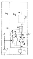
図示の光エレクトリックセルは、送信アセンブリ10と受信アセンブリ20とを備えている。送信アセンブリは、低い周期割合でパルス化信号E1を発生している。このパルス化信号は、フォトダイオード等の発光コンポーネント11へ送信される。受信アセンブリ20は、光トランジスタ等の受光コンポーネント21を備えている。この受光コンポーネントは、電流信号Iを生成することにより、信号E1のパルスに応答する。電流信号Iがハイかロウかは、コンポーネント11により発せられた光ビームの経路に物体が存在するか存在しないかに、依存する。受信アセンブリ20は、回路22も備えている。この回路22は、装置23による処理が可能な電圧信号S1を生成するために、信号Iを用いる。この装置23は、ハイ又はロウのスイッチング信号Sを供給し、セルの出力振幅を生成する。
【0009】
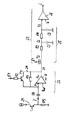
回路22は、負荷増幅器A又は伝達インピーダンス増幅器(transfer impedance amplifier)を有している。これは、入力A1に電流信号Iが入力され、入力A2に基準電圧Vrefが入力され、その信号出力から電圧信号S1を出力する。増幅器の出力A3は装置23へ接続されている。この装置23は、積分・フィルタリング回路25と、比較器26とを、備えている。この比較器26は、フィルタリングされた結果の信号と、しきい値電圧Vcとを比較して、オン/オフのスイッチング信号Sを出力する。
【0010】
増幅器の入力A1は、抵抗R1が設けられたゲインループ24を介して、増幅器の出力A3に、接続されている。短絡経路24aがこのループと並列に接続されている。この短絡経路には、信号E1により動作するトランジスタT1が設けられている。このため、短絡経路は、送信パルスが存在しているときは導通せず、そのようなパルスが存在しないときは導通するようになる。経路24aが増幅器の出力A3へ接続するポイントと、比較器26との間には、トランジスタT2と積分・フィルタリング回路25とが、連続的に配置されている。トランジスタT2は、信号E1により操作され、送信パルスが存在するときのみ導通する。積分・フィルタリング回路25は、積分化された電圧信号S2を生成するために、電圧信号S1を使用する。電圧信号S2に積分化された電圧信号S3が続き、信号Sから不必要な特性を取り除く。特に、セルに影響を与える短時間の電気的外乱、とりわけ、検出可能なパルスの受信の直前に起きた外乱を、取り除く。
【0011】
図2に示す実施形態においては、トランジスタT1はPNP型バイポーラトランジスタであり、そのベースは抵抗R2を介してE1により操作される。トランジスタT2はMOSトランジスタである。回路23は、T2に接続された積分器R3、C2と、フィルタリングネットワークR4、C3とを、備えている。大型化し且つ正確性が落ちるという利点が減少した実施形態にあっては、回路23をフリップフロップで構成してもよい。
【0012】
増幅器A1の入力A1の前段には、キャパシタC4が配置されている。抵抗R5は、光トランジスタ21の送信用の脚を構成する。キャパシタC4とともに、ゲイン抵抗R1と抵抗R5とは、低周波ノイズを除去するハイパスフィルターを構成する。
【0013】
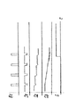
ここで、このセルの機能を図3に基づいて説明する。
【0014】
送信信号E1からのパルスが存在しない場合、トランジスタT2は導通せず、このため、比較器26の入力はハイレベルを維持する。もし短時間の電源ラインの外乱が検出された場合、それは経路24aを用いて増幅器のゲイン抵抗R1を短絡するトランジスタT1によって、迂回する。したがって、増幅器はトラッキングモードで動作する。これは、次のパルスに有害な影響を及ぼす長い減衰時間の信号の発生を防止する。
【0015】
送信信号E1からのパルスが存在する場合、トランジスタT1は導通せず、トランジスタT2は導通する。照射ビームの経路に物体が位置すると、対応するレベルの電流信号Iが生成され、この電流信号Iは増幅器Aで電圧信号S1に変換される。信号のリーディングエッジに存在する外乱データは取り除かれているので、信号S1は正確に対応する送信信号を代表している。信号S2は連続的なパルスにより管理されて各段毎に減退する。信号S3はフィルタリングされており、このため、比較器の入力で図3に示すように整った形で減退する。S3がしきい値Vcに到達すると、直ちに、処理回路により供給されていたスイッチング信号Sはレベルを切り替える。
【図面の簡単な説明】
【図1】本発明に係る光エレクトリックセルの概略図。
【図2】本発明の一例をより詳しく示した図。
【図3】図1及び図2における電気的振幅の変化を示すグラフ。
Claims (3)
- パルス化された送信信号(E1)を発生する電気的回路と、
前記信号が入力される発光コンポーネントと、
を有する送信アセンブリを備えた光エレクトリックセルであって、
当該光エレクトリックセルは、
受光コンポーネントと、
前記受光コンポーネントから供給される受信信号(I)の処理をするための回路(22)と、
を有する受信アセンブリも備えるとともに、
前記回路は、前記受信信号(I)が直接入力される入力(A1)と、スイッチング信号(S)を生成する装置(23)へ電圧信号(S1)を供給する出力(A3)とを、有する増幅器(A)を備え、
前記増幅器(A)は、前記出力(A3)をゲイン抵抗(R1)を介して前記入力(A1)に接続するゲインループ(24)と、前記ゲインループに並列に導出経路(24a)とが設けられている、伝達インピーダンス増幅器であり、前記導出経路(24a)にはスイッチ(T1)が設けられており、且つ、前記スイッチ(T1)は、パルス化された前記送信信号(E1)によりコントロールされ、
前記スイッチは前記送信信号からのパルスが存在するときは導通せず、
そのようなパルスが存在しないときは導通して、前記増幅器(A)の前記出力(A3)と前記入力(A1)とが、前記導出経路(24a)を介して、前記スイッチ(T1)により短絡する、
ことを特徴とする光エレクトリックセル。 - 前記受信アセンブリ(20)は、信号パルスを送信する期間以外は、処理を停止するための手段を備えており、
前記停止手段は、前記増幅器(A)の前記出力に設けられた、且つ、パルス信号(E1)によりコントロールされる、トランジスタ(T2)であり、それはパルス信号が存在するときは導通する、
ことを特徴とする請求項1に記載のセル。 - 前記スイッチング信号(S)を生成する装置(23)は、
いくつかのパルスの電圧信号(S1)をフィルタリングする積分・フィルタリング回路(25)と、
積分化されフィルタリングされた前記信号(S3)としきい値(Vc)とを比較する比較器(26)と、
を備えたことを特徴とする請求項1に記載のセル。
Applications Claiming Priority (2)
| Application Number | Priority Date | Filing Date | Title |
|---|---|---|---|
| FR9614914A FR2756682B1 (fr) | 1996-12-03 | 1996-12-03 | Cellule photoelectrique a amplification stabilisee |
| FR9614914 | 1996-12-03 |
Publications (2)
| Publication Number | Publication Date |
|---|---|
| JPH114197A JPH114197A (ja) | 1999-01-06 |
| JP4046820B2 true JP4046820B2 (ja) | 2008-02-13 |
Family
ID=9498351
Family Applications (1)
| Application Number | Title | Priority Date | Filing Date |
|---|---|---|---|
| JP33165597A Expired - Fee Related JP4046820B2 (ja) | 1996-12-03 | 1997-12-02 | 安定化増幅器を有する光エレクトリックセル |
Country Status (6)
| Country | Link |
|---|---|
| US (1) | US5994689A (ja) |
| JP (1) | JP4046820B2 (ja) |
| CH (1) | CH692164A5 (ja) |
| DE (1) | DE19753472B4 (ja) |
| FR (1) | FR2756682B1 (ja) |
| IT (1) | IT1296601B1 (ja) |
Families Citing this family (39)
| Publication number | Priority date | Publication date | Assignee | Title |
|---|---|---|---|---|
| JPS48101243U (ja) * | 1972-03-01 | 1973-11-28 | ||
| JPS494838A (ja) * | 1972-05-02 | 1974-01-17 | ||
| JPS5334840B2 (ja) * | 1974-01-31 | 1978-09-22 | ||
| DE59812595D1 (de) | 1997-12-11 | 2005-03-31 | Sel Alcatel Ag | Optischer Empfänger für den empfang von digital übertragenen Daten |
| US6061551A (en) | 1998-10-21 | 2000-05-09 | Parkervision, Inc. | Method and system for down-converting electromagnetic signals |
| US7515896B1 (en) | 1998-10-21 | 2009-04-07 | Parkervision, Inc. | Method and system for down-converting an electromagnetic signal, and transforms for same, and aperture relationships |
| US6542722B1 (en) | 1998-10-21 | 2003-04-01 | Parkervision, Inc. | Method and system for frequency up-conversion with variety of transmitter configurations |
| US7295826B1 (en) | 1998-10-21 | 2007-11-13 | Parkervision, Inc. | Integrated frequency translation and selectivity with gain control functionality, and applications thereof |
| US7027786B1 (en) * | 1998-10-21 | 2006-04-11 | Parkervision, Inc. | Carrier and clock recovery using universal frequency translation |
| US7236754B2 (en) | 1999-08-23 | 2007-06-26 | Parkervision, Inc. | Method and system for frequency up-conversion |
| US6560301B1 (en) | 1998-10-21 | 2003-05-06 | Parkervision, Inc. | Integrated frequency translation and selectivity with a variety of filter embodiments |
| US6813485B2 (en) | 1998-10-21 | 2004-11-02 | Parkervision, Inc. | Method and system for down-converting and up-converting an electromagnetic signal, and transforms for same |
| US6370371B1 (en) | 1998-10-21 | 2002-04-09 | Parkervision, Inc. | Applications of universal frequency translation |
| US7039372B1 (en) | 1998-10-21 | 2006-05-02 | Parkervision, Inc. | Method and system for frequency up-conversion with modulation embodiments |
| US6853690B1 (en) | 1999-04-16 | 2005-02-08 | Parkervision, Inc. | Method, system and apparatus for balanced frequency up-conversion of a baseband signal and 4-phase receiver and transceiver embodiments |
| US6873836B1 (en) | 1999-03-03 | 2005-03-29 | Parkervision, Inc. | Universal platform module and methods and apparatuses relating thereto enabled by universal frequency translation technology |
| US6879817B1 (en) | 1999-04-16 | 2005-04-12 | Parkervision, Inc. | DC offset, re-radiation, and I/Q solutions using universal frequency translation technology |
| US7110435B1 (en) | 1999-03-15 | 2006-09-19 | Parkervision, Inc. | Spread spectrum applications of universal frequency translation |
| US7110444B1 (en) | 1999-08-04 | 2006-09-19 | Parkervision, Inc. | Wireless local area network (WLAN) using universal frequency translation technology including multi-phase embodiments and circuit implementations |
| US7693230B2 (en) | 1999-04-16 | 2010-04-06 | Parkervision, Inc. | Apparatus and method of differential IQ frequency up-conversion |
| US7065162B1 (en) | 1999-04-16 | 2006-06-20 | Parkervision, Inc. | Method and system for down-converting an electromagnetic signal, and transforms for same |
| US6069377A (en) * | 1999-05-13 | 2000-05-30 | Eastman Kodak Company | Image sensor incorporating saturation time measurement to increase dynamic range |
| US8295406B1 (en) | 1999-08-04 | 2012-10-23 | Parkervision, Inc. | Universal platform module for a plurality of communication protocols |
| US7072390B1 (en) | 1999-08-04 | 2006-07-04 | Parkervision, Inc. | Wireless local area network (WLAN) using universal frequency translation technology including multi-phase embodiments |
| US7054296B1 (en) | 1999-08-04 | 2006-05-30 | Parkervision, Inc. | Wireless local area network (WLAN) technology and applications including techniques of universal frequency translation |
| US7082171B1 (en) | 1999-11-24 | 2006-07-25 | Parkervision, Inc. | Phase shifting applications of universal frequency translation |
| US7292835B2 (en) | 2000-01-28 | 2007-11-06 | Parkervision, Inc. | Wireless and wired cable modem applications of universal frequency translation technology |
| US7010286B2 (en) | 2000-04-14 | 2006-03-07 | Parkervision, Inc. | Apparatus, system, and method for down-converting and up-converting electromagnetic signals |
| US7554508B2 (en) | 2000-06-09 | 2009-06-30 | Parker Vision, Inc. | Phased array antenna applications on universal frequency translation |
| US7010559B2 (en) | 2000-11-14 | 2006-03-07 | Parkervision, Inc. | Method and apparatus for a parallel correlator and applications thereof |
| US7454453B2 (en) | 2000-11-14 | 2008-11-18 | Parkervision, Inc. | Methods, systems, and computer program products for parallel correlation and applications thereof |
| US7072427B2 (en) | 2001-11-09 | 2006-07-04 | Parkervision, Inc. | Method and apparatus for reducing DC offsets in a communication system |
| US7085335B2 (en) * | 2001-11-09 | 2006-08-01 | Parkervision, Inc. | Method and apparatus for reducing DC offsets in a communication system |
| JP4166466B2 (ja) * | 2001-12-19 | 2008-10-15 | ソニー株式会社 | 無線通信システム及び無線通信方法、無線通信装置及びその制御方法、並びにコンピュータ・プログラム |
| US6975848B2 (en) | 2002-06-04 | 2005-12-13 | Parkervision, Inc. | Method and apparatus for DC offset removal in a radio frequency communication channel |
| US7321640B2 (en) | 2002-06-07 | 2008-01-22 | Parkervision, Inc. | Active polyphase inverter filter for quadrature signal generation |
| US7379883B2 (en) | 2002-07-18 | 2008-05-27 | Parkervision, Inc. | Networking methods and systems |
| US7460584B2 (en) | 2002-07-18 | 2008-12-02 | Parkervision, Inc. | Networking methods and systems |
| US20050177131A1 (en) * | 2004-02-09 | 2005-08-11 | Lentz David J. | Catheter articulation segment with alternating cuts |
Family Cites Families (4)
| Publication number | Priority date | Publication date | Assignee | Title |
|---|---|---|---|---|
| US3739177A (en) * | 1970-12-15 | 1973-06-12 | North American Mfg Co | Light sensitive control |
| JP2558459B2 (ja) * | 1987-04-15 | 1996-11-27 | アルプス電気株式会社 | 光電検出回路 |
| US4861978A (en) * | 1987-11-25 | 1989-08-29 | Anderson Thor W | Automatic gain setting circuit |
| JPH05136678A (ja) * | 1991-11-11 | 1993-06-01 | Yamatake Honeywell Co Ltd | 光電スイツチ |
-
1996
- 1996-12-03 FR FR9614914A patent/FR2756682B1/fr not_active Expired - Fee Related
-
1997
- 1997-11-28 CH CH02750/97A patent/CH692164A5/fr not_active IP Right Cessation
- 1997-12-02 IT IT97TO001048A patent/IT1296601B1/it active IP Right Grant
- 1997-12-02 DE DE19753472A patent/DE19753472B4/de not_active Expired - Fee Related
- 1997-12-02 JP JP33165597A patent/JP4046820B2/ja not_active Expired - Fee Related
- 1997-12-03 US US08/984,063 patent/US5994689A/en not_active Expired - Lifetime
Also Published As
| Publication number | Publication date |
|---|---|
| DE19753472A1 (de) | 1998-06-04 |
| ITTO971048A0 (it) | 1997-12-02 |
| FR2756682B1 (fr) | 1999-05-14 |
| FR2756682A1 (fr) | 1998-06-05 |
| JPH114197A (ja) | 1999-01-06 |
| US5994689A (en) | 1999-11-30 |
| ITTO971048A1 (it) | 1999-06-02 |
| IT1296601B1 (it) | 1999-07-14 |
| DE19753472B4 (de) | 2007-01-11 |
| CH692164A5 (fr) | 2002-02-28 |
Similar Documents
| Publication | Publication Date | Title |
|---|---|---|
| JP4046820B2 (ja) | 安定化増幅器を有する光エレクトリックセル | |
| US4764732A (en) | Switchable mode amplifier for wide dynamic range | |
| US4498001A (en) | Transimpedance amplifier for optical receivers | |
| US4369525A (en) | Device for automatic regulation of the output power of a transmitter module in an optical-fiber transmission system | |
| US5822104A (en) | Digital optical receiving apparatus | |
| US6057738A (en) | High dynamic range optical receiver preamplifier | |
| US4851689A (en) | Photodetecting circuit | |
| JP2010093353A (ja) | 光受信器 | |
| US5111324A (en) | Optical receivers | |
| US5517351A (en) | Optical receiver apparatus | |
| US4792998A (en) | Receiver for optical digital signals having different amplitudes | |
| US6909081B2 (en) | Evaluation circuit for processing the output of a light detector | |
| CN209930268U (zh) | 光接收模块和光模块 | |
| US5561383A (en) | Switchable peak/average detect circuit | |
| DK173749B1 (da) | Optisk sender | |
| AU4216985A (en) | Apparatus for increasing the dynamic range in an integrating optoelectric receiver | |
| KR100195281B1 (ko) | 노이즈를 개선한 헤드-앰프 | |
| CA1234872A (en) | Edge detection using dual trans-impedance amplifier | |
| JPH04598Y2 (ja) | ||
| CN114726319B (zh) | 一种脉冲电流信号的放大电路及其工作方法 | |
| CN118282338A (zh) | 一种基于跨阻放大器的盖革放大器电路 | |
| KR930008016Y1 (ko) | 광수신기의 적응적 광상태 판별회로 | |
| SU1084967A1 (ru) | Эмиттерный повторитель | |
| JPH01205610A (ja) | 光受信回路 | |
| CN120165677A (zh) | Pon中雪崩光电二极管保护电路和pon光猫 |
Legal Events
| Date | Code | Title | Description |
|---|---|---|---|
| A621 | Written request for application examination |
Free format text: JAPANESE INTERMEDIATE CODE: A621 Effective date: 20040720 |
|
| A977 | Report on retrieval |
Free format text: JAPANESE INTERMEDIATE CODE: A971007 Effective date: 20061017 |
|
| A131 | Notification of reasons for refusal |
Free format text: JAPANESE INTERMEDIATE CODE: A131 Effective date: 20061031 |
|
| A521 | Request for written amendment filed |
Free format text: JAPANESE INTERMEDIATE CODE: A523 Effective date: 20070109 |
|
| A131 | Notification of reasons for refusal |
Free format text: JAPANESE INTERMEDIATE CODE: A131 Effective date: 20070511 |
|
| A521 | Request for written amendment filed |
Free format text: JAPANESE INTERMEDIATE CODE: A523 Effective date: 20070801 |
|
| TRDD | Decision of grant or rejection written | ||
| A01 | Written decision to grant a patent or to grant a registration (utility model) |
Free format text: JAPANESE INTERMEDIATE CODE: A01 Effective date: 20071023 |
|
| A61 | First payment of annual fees (during grant procedure) |
Free format text: JAPANESE INTERMEDIATE CODE: A61 Effective date: 20071121 |
|
| FPAY | Renewal fee payment (event date is renewal date of database) |
Free format text: PAYMENT UNTIL: 20101130 Year of fee payment: 3 |
|
| R150 | Certificate of patent or registration of utility model |
Free format text: JAPANESE INTERMEDIATE CODE: R150 |
|
| FPAY | Renewal fee payment (event date is renewal date of database) |
Free format text: PAYMENT UNTIL: 20101130 Year of fee payment: 3 |
|
| S531 | Written request for registration of change of domicile |
Free format text: JAPANESE INTERMEDIATE CODE: R313531 |
|
| FPAY | Renewal fee payment (event date is renewal date of database) |
Free format text: PAYMENT UNTIL: 20101130 Year of fee payment: 3 |
|
| R360 | Written notification for declining of transfer of rights |
Free format text: JAPANESE INTERMEDIATE CODE: R360 |
|
| R370 | Written measure of declining of transfer procedure |
Free format text: JAPANESE INTERMEDIATE CODE: R370 |
|
| FPAY | Renewal fee payment (event date is renewal date of database) |
Free format text: PAYMENT UNTIL: 20101130 Year of fee payment: 3 |
|
| FPAY | Renewal fee payment (event date is renewal date of database) |
Free format text: PAYMENT UNTIL: 20101130 Year of fee payment: 3 |
|
| S531 | Written request for registration of change of domicile |
Free format text: JAPANESE INTERMEDIATE CODE: R313531 |
|
| FPAY | Renewal fee payment (event date is renewal date of database) |
Free format text: PAYMENT UNTIL: 20101130 Year of fee payment: 3 |
|
| R350 | Written notification of registration of transfer |
Free format text: JAPANESE INTERMEDIATE CODE: R350 |
|
| FPAY | Renewal fee payment (event date is renewal date of database) |
Free format text: PAYMENT UNTIL: 20111130 Year of fee payment: 4 |
|
| FPAY | Renewal fee payment (event date is renewal date of database) |
Free format text: PAYMENT UNTIL: 20111130 Year of fee payment: 4 |
|
| FPAY | Renewal fee payment (event date is renewal date of database) |
Free format text: PAYMENT UNTIL: 20121130 Year of fee payment: 5 |
|
| FPAY | Renewal fee payment (event date is renewal date of database) |
Free format text: PAYMENT UNTIL: 20121130 Year of fee payment: 5 |
|
| FPAY | Renewal fee payment (event date is renewal date of database) |
Free format text: PAYMENT UNTIL: 20131130 Year of fee payment: 6 |
|
| R250 | Receipt of annual fees |
Free format text: JAPANESE INTERMEDIATE CODE: R250 |
|
| R250 | Receipt of annual fees |
Free format text: JAPANESE INTERMEDIATE CODE: R250 |
|
| LAPS | Cancellation because of no payment of annual fees |