JP4042340B2 - Information equipment - Google Patents
Information equipment Download PDFInfo
- Publication number
- JP4042340B2 JP4042340B2 JP2001106722A JP2001106722A JP4042340B2 JP 4042340 B2 JP4042340 B2 JP 4042340B2 JP 2001106722 A JP2001106722 A JP 2001106722A JP 2001106722 A JP2001106722 A JP 2001106722A JP 4042340 B2 JP4042340 B2 JP 4042340B2
- Authority
- JP
- Japan
- Prior art keywords
- module
- data
- function
- unit
- devices
- Prior art date
- Legal status (The legal status is an assumption and is not a legal conclusion. Google has not performed a legal analysis and makes no representation as to the accuracy of the status listed.)
- Expired - Lifetime
Links
Images


Classifications
-
- G—PHYSICS
- G04—HOROLOGY
- G04G—ELECTRONIC TIME-PIECES
- G04G17/00—Structural details; Housings
-
- G—PHYSICS
- G04—HOROLOGY
- G04G—ELECTRONIC TIME-PIECES
- G04G21/00—Input or output devices integrated in time-pieces
-
- A—HUMAN NECESSITIES
- A44—HABERDASHERY; JEWELLERY
- A44C—PERSONAL ADORNMENTS, e.g. JEWELLERY; COINS
- A44C5/00—Bracelets; Wrist-watch straps; Fastenings for bracelets or wrist-watch straps
- A44C5/0007—Bracelets specially adapted for other functions or with means for attaching other articles
- A44C5/0015—Bracelets specially adapted for other functions or with means for attaching other articles providing information, e.g. bracelets with calendars
-
- G—PHYSICS
- G04—HOROLOGY
- G04G—ELECTRONIC TIME-PIECES
- G04G17/00—Structural details; Housings
- G04G17/08—Housings
- G04G17/083—Watches distributed over several housings
-
- G—PHYSICS
- G04—HOROLOGY
- G04G—ELECTRONIC TIME-PIECES
- G04G21/00—Input or output devices integrated in time-pieces
- G04G21/02—Detectors of external physical values, e.g. temperature
-
- G—PHYSICS
- G06—COMPUTING; CALCULATING OR COUNTING
- G06F—ELECTRIC DIGITAL DATA PROCESSING
- G06F1/00—Details not covered by groups G06F3/00 - G06F13/00 and G06F21/00
- G06F1/16—Constructional details or arrangements
- G06F1/1613—Constructional details or arrangements for portable computers
- G06F1/163—Wearable computers, e.g. on a belt
-
- H—ELECTRICITY
- H04—ELECTRIC COMMUNICATION TECHNIQUE
- H04B—TRANSMISSION
- H04B1/00—Details of transmission systems, not covered by a single one of groups H04B3/00 - H04B13/00; Details of transmission systems not characterised by the medium used for transmission
- H04B1/38—Transceivers, i.e. devices in which transmitter and receiver form a structural unit and in which at least one part is used for functions of transmitting and receiving
- H04B1/3827—Portable transceivers
- H04B1/385—Transceivers carried on the body, e.g. in helmets
-
- H—ELECTRICITY
- H04—ELECTRIC COMMUNICATION TECHNIQUE
- H04M—TELEPHONIC COMMUNICATION
- H04M1/00—Substation equipment, e.g. for use by subscribers
- H04M1/02—Constructional features of telephone sets
- H04M1/0202—Portable telephone sets, e.g. cordless phones, mobile phones or bar type handsets
- H04M1/0254—Portable telephone sets, e.g. cordless phones, mobile phones or bar type handsets comprising one or a plurality of mechanically detachable modules
-
- H—ELECTRICITY
- H04—ELECTRIC COMMUNICATION TECHNIQUE
- H04B—TRANSMISSION
- H04B1/00—Details of transmission systems, not covered by a single one of groups H04B3/00 - H04B13/00; Details of transmission systems not characterised by the medium used for transmission
- H04B1/38—Transceivers, i.e. devices in which transmitter and receiver form a structural unit and in which at least one part is used for functions of transmitting and receiving
- H04B1/3827—Portable transceivers
- H04B1/385—Transceivers carried on the body, e.g. in helmets
- H04B2001/3855—Transceivers carried on the body, e.g. in helmets carried in a belt or harness
-
- H—ELECTRICITY
- H04—ELECTRIC COMMUNICATION TECHNIQUE
- H04M—TELEPHONIC COMMUNICATION
- H04M1/00—Substation equipment, e.g. for use by subscribers
- H04M1/72—Mobile telephones; Cordless telephones, i.e. devices for establishing wireless links to base stations without route selection
- H04M1/724—User interfaces specially adapted for cordless or mobile telephones
- H04M1/72403—User interfaces specially adapted for cordless or mobile telephones with means for local support of applications that increase the functionality
- H04M1/72409—User interfaces specially adapted for cordless or mobile telephones with means for local support of applications that increase the functionality by interfacing with external accessories
- H04M1/72412—User interfaces specially adapted for cordless or mobile telephones with means for local support of applications that increase the functionality by interfacing with external accessories using two-way short-range wireless interfaces
-
- H—ELECTRICITY
- H04—ELECTRIC COMMUNICATION TECHNIQUE
- H04M—TELEPHONIC COMMUNICATION
- H04M2250/00—Details of telephonic subscriber devices
- H04M2250/12—Details of telephonic subscriber devices including a sensor for measuring a physical value, e.g. temperature or motion
Description
【0001】
【発明の属する技術分野】
【0002】
本発明は、身体装着可能な情報機器に関する。
【0003】
【従来の技術】
【0004】
従来、腕時計においては、時計回路や時計ムーブメント、電池などの時計として必須の構成部品以外に、各種センサーや機能回路を組み込んで内蔵し、時計本体の周部に設けられているキー入力部の操作により、時刻表示以外の各種機能を発生させる得るものが実用化されている。また、リストバンドに磁気コンパスなどの追加ユニットを着脱自在に取り付け、この追加ユニットによる機能を更に付加することも実用化されている。
【0005】
【発明が解決しようとする課題】
【0006】
このように、時計本体内に各種機能回路等を組み込んだ場合、時計回路の制御部や表示部を有効利用して各機能回路を制御し、機能に応じた結果を表示することができる利点がある。その反面、各機能回路等を時計本体に内蔵すると、多機能化に伴って時計本体が大型化することとなり、また、腕に装着する機器である腕時計の性質上、時計本体が大型化には自ずと限界があり、多機能化に十分対応することができない。
【0007】
これに対し、バンドに追加ユニットを取り付ける構成の場合、時計本体内への各種回路や部品の増設がないことから時計本体の大型化が伴うことがない利点がある。その反面、時計回路の制御部や表示部を利用して各ユニット回路の制御を行うことができず、各ユニット毎に制御部や表示部を設けることが必要となってしまう。
【0008】
本発明は、このような従来の課題に鑑みてなされたものであり、腕時計等のリスト装置における本体の大型化を伴うことなく、構成の簡単化を図りつつ多機能化に対応することのできる身体装着可能な情報機器を提供することを目的とするものである。
【0009】
【課題を解決するための手段】
【0010】
前記課題を解決するために請求項1記載の発明にかかる身体装着可能な情報機器にあっては、データを表示する表示部と、使用者の身体に着脱可能に装着されるバンド部と、前記バンド部に着脱自在に装着される複数の機器と、前記バンド部に着脱自在に装着され予め定められている電源容量を有する複数の電源と、前記バンド部に複数の機器が装着され、かつ、複数の電源が装着されたことを条件に、この装着された複数の機器の合計消費電力値と前記複数の電源の合計容量値とを比較判断し、前記複数の機器の合計消費電力値が前記複数の電源の合計容量値を超えたと比較判断した際は、前記機器の前記バンド部からの取り外しと前記電源の前記バンド部への追加装着とのいずれか一方の指示を前記表示部に出力する出力手段とを備えていることを特徴とする。
【0011】
また、請求項2記載の発明にかかる身体装着可能な情報機器にあっては、データを表示する表示部を備えているケース本体と、電子回路を内蔵する複数の機器と、前記複数の機器を連結部材により互いに着脱自在に連結して成るバンド部と、前記バンド部に着脱自在に装着され予め定められている電源容量を有する複数の電源と、前記バンド部に複数の機器が装着され、かつ、複数の電源が装着されたことを条件に、この装着された複数の機器の合計消費電力値と前記複数の電源の合計容量値とを比較判断し、前記複数の機器の合計消費電力値が前記複数の電源の合計容量値を超えたと比較判断した際は、前記機器の前記バンド部からの取り外しと前記電源の前記バンド部への追加装着とのいずれか一方の指示を前記表示部に出力し、前記複数の機器の合計消費電力値が前記複数の電源の合計容量値を超えていないと比較判断した際は、前記複数の機器の合計消費電力値と前記複数の電源の合計容量値とを前記前記表示部に出力する出力手段とを備えていることを特徴とする。
【0012】
また、請求項3記載の発明にかかる身体装着可能な情報機器にあっては、前記ケース本体は、前記電子回路に接続された第1の信号端子を有し、前記複数の機器は、前記電子回路に接続された信号線とこの信号線の両端に設けられている第2の信号端子とを備え、前記複数の機器を互いに前記第2の信号端子で電気的に接続するとともに、前記ケース本体と機器とを前記第1の信号端子と第2の信号端子とにより電気的に接続したことを特徴とする。
【0013】
また、請求項4記載の発明にかかる身体装着可能な情報機器にあっては、請求項3記載の情報機器において、前記複数の機器には、前記電子回路を内蔵しない機器が含まれ、該機器は前記信号線とこの信号線の両端に設けられている第2の信号端子から成ることを特徴とする。
【0014】
また、請求項5記載の発明にかかる身体装着可能な情報機器にあっては、データを表示する表示部を備えているケース本体と、このケース本体に設けられ、かつ、内部に電磁誘導発生用の第1のコイルを配置した使用者の身体に着脱可能に装着されるバンド部と、内部に電磁誘導発生用の第2のコイルを備え、前記バンド部に着脱自在に装着される複数の機器と、前記バンド部に着脱自在に装着され予め定められている電源容量を有する複数の電源と、前記第1のコイルと第2のコイルとの間で、データ及び電源電流の内の少なくとも一方を転送させるように制御する転送制御手段と、前記バンド部に複数の機器が装着され、かつ、複数の電源が装着されたことを条件に、この装着された複数の機器の合計消費電力値と前記複数の電源の合計容量値とを比較判断し、前記複数の機器の合計消費電力値が前記複数の電源の合計容量値を超えたと比較判断した際は、前記機器の前記バンド部からの取り外しと前記電源の前記バンド部への追加装着とのいずれか一方の指示を前記表示部に出力する出力手段とを備えていることを特徴とする。
【0027】
【発明の実施の形態】
【0028】
(1)第1の実施の形態
【0029】
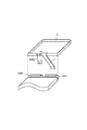
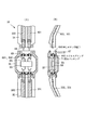
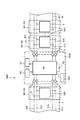
以下、本発明の第1の実施の形態を図に従って説明する。図1は本発明の一実施の形態にかかる腕時計1の外観図を示すものであり、(A)は腕時計1の全体図、(B)は表示部60の拡大図である。図1(A)に示すように腕時計1は、時計本体ケース6と、この時計本体ケース6の相対向する端部に取り付けられた一対の樹脂製のリストバンド4、5とを有している。リストバンド4は図2に示されるように、尾錠通し穴4001と切り欠き部4002により尾錠2と着脱可能に接合されている。また、突く棒11は尾錠2のスペース2001から矢印の方向に挿入され、その後、突く棒11の径より十分大きいピン2002によって尾錠に回動可能に固定される。
【0030】
これは後述する機能モジュール80、81を接続あるいは交換する際、尾錠2および突く棒11を取り外すことによって、容易に行えるようにするためである。
【0031】
リストバンド4にはメモリ機能を有する機能モジュール80,81が着脱自在に取り付けられている。また、他方のリストバンド5には、温度センサ機能を有する機能モジュール82、圧力センサ機能を有する機能モジュール83、及び電子方位センサ機能を有する機能モジュール84が着脱自在に取り付けられている。
【0032】
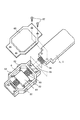
時計本体ケース6の上面には、LCDからなり、後述する制御回路部63からの制御に基づく時刻情報、及び後述する機能モジュール80〜84の各機能に基づく情報を表示する機能を備える表示部60が設けられており、側面には複数のキー操作部62が設けられている。時計本体ケース6内部には、図3に示すように、前記表示部60の下面側に順次制御回路部63と電池64とが配置され、時計本体ケース6の裏面側は時計バックケース66により閉鎖されている。制御回路部63は、図4に示すように、前記複数のキー操作部62に接続されているとともに、前記リストバンド4、5が取り付けられた端部方向に延びる4本のバス接続バネ65により、弾性的にリストバンド4、5に設けられた本体接続用プラグ68と接続される。
【0033】
また、時計本体ケース6の相対向する端部には、バス接続用レセプタクル69が設けられている。
【0034】
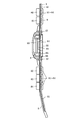
前記リストバンド4の端部には、図1(A)に示すように、遊環3、尾錠2及び突く棒11が取り付けられており、両リストバンド4、5には、各々バス配線41、51が長手方向に沿って埋設されている。各バス配線41、51は、電源(Vcc)線411、511、データ信号(Serial Data)線412、512、クロック信号(Clock)線413、513、及び接地(GND)線414、514で構成されている。これらバス配線41、51を構成する各線411〜514には、図4に示すように、前記機能モジュール80〜84に対応する位置でリストバンド4、5の裏面側に露出した接続端子(電源(Vcc)線用)91、接続端子(データ信号(Serial Data)線用)92、接続端子(クロック信号(Clock)線用)93、接続端子(接地(GND)線用)94が設けられている。また、バス配線41、51を構成する各線411〜514の端部は、各リストバンド4、5の端部に設けられた本体接続用プラグ68に接続されている。
【0035】
そして、図3に示したように、この本体接続用プラグ68をバス接続用レセプタクル69に差し込んでバス接続バネ65に端部に接触させる。この状態で時計バックケース66を固定するための固定用ビス67により、時計本体ケース6の端部とリストバンド4、5の端部とを共締めすることによって、時計本体ケース6側とリストバンド4、5側とが電気的に接続されている。
【0036】
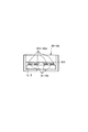
前記機能モジュール80〜84は、図6に示すように、外形が直方体であって環状に形成されており、一面側に機能モジュール内蔵回路800を有し、この機能モジュール内蔵回路800に対向する内面に4個の接続端子801〜804を有している。これら4個の接続端子801〜804は、機能モジュール80〜84をリストバンド4、5に嵌合させた状態において、各接続端子91〜94と接触し得る位置に設けられている。
【0037】
したがって、機能モジュール80〜84をリストバンド4、5に嵌合させると、機能モジュール80〜84の各機能モジュール内蔵回路800は、接続端子91〜94、801〜804を介して、図7及び図8に示すように、電源(Vcc)線411、511、データ信号(Serial Data)線412、512、クロック信号(Clock)線413、513、及び接地(GND)線414、514に接続され、さらに本体接続用プラグ68とバス接続バネ65を介して時計本体ケース6内の制御回路部63に接続されることとなる。また、図7に示すように、時計本体ケース6内には、前記制御回路部63と前記制御回路部63に電力を供給する電池64とが内蔵されるとともに、前記表示部60と前記キー操作部62とが時計本体ケース6の外周部に向かって配置される。
【0038】
図9は、機能モジュール80〜84の回路構成図であり、各機能モジュール80〜84は、接続端子91〜94にて、前記電源(Vcc)線411、データ信号(Serial Data)線412、クロック信号(Clock)線413、接地(GND)線414に接続される。メモリ機能を有する機能モジュール80、81は、図9(A)に示すように、接続端子91に接続された電源制御部812、接続端子92、93に接続されたI/O制御回路部811を有するとともに、コマンド/アドレスレジスタ813、データレジスタ814、CRC(Cyclic Rendundancy Check)生成部815、ROM816、メモリ817を有している。ROM816には、当該機能モジュールに固有のモジュールIDデータやシリアルNo.データ等の識別情報が記憶されている。
【0039】
センサ機能を有する機能モジュール82〜84は、同図(B)に示すように、同様にI/O制御回路部811、電源制御部812、コマンド/アドレスレジスタ813、データレジスタ814、CRC生成部815、ROM816、メモリ817を有するとともに、センサ制御部831、センサデータメモリ832、A/D変換器833、アンプ834、センサ835を有している。
【0040】
図10は、時計本体ケース6側と機能モジュール80〜84側との間で送受信されるデータの構成例を示すものである。本例では、同図(A)に示すように、スタートビットSとストップビットPとを用いる所謂調歩式(非同期式)で、スタートビットSで送信を開始し、8ビットずつシリアル伝送し、最後にストップビットPを送信して終了する。受信側では各8ビット毎にデータの受信を確認すると、確認応答信号ACKをデータ送信側に返信する。このとき、制御回路部63から伝送するシリアルデータは、同図(B)に例示するように、スタートビットSが先頭部、ストップビットPが末尾部にそれぞれ設定され、8ビット単位で同期信号SYとパリティチェックビットPAとの間に設定された、コマンドデータ信号(C0〜C2:3ビット)、モジュールIDデータ信号(ID0〜ID4:5ビット)、リード/ライト制御信号(R/W:1ビット)、アドレスデータ信号(A0〜A7:8ビット)、データ信号(D0〜D15:16ビット)、及びCRC符号/エラー訂正符号(CR0〜CR7:8ビット)と設定されており、8ビット単位で受信側から送信される確認応答信号ACKの受信を確認できるようになっている。
【0041】
図11(A)は、制御回路部63から接続端子92を介して機能モジュール80〜84に伝送されるシリアルデータのデータ構成を示すものであり、同図に示すように、同期信号SY、データ信号(C、ID、R/W、A、D、CR)及びパリティチェックビットPAを一組とする所定単位のデータで構成される。このシリアルデータは、同図(B)に示すように、機能モジュール80〜84側にて復号される。そしてこれら復号されたデータ信号(C、ID、R/W、A、D、CR)は、同図(C)に示すように、コマンドデータ、リード/ライト制御データ、モジュールIDデータ、アドレスデータ、データ(実データ)、CRC符号/エラー訂正符号で構成される。
【0042】
なお、本実施の形態では、同期信号SYを設定するようにしているが、確認応答信号ACKを同期信号SYの代わりに設定してもよい。
【0043】
また、ACK(確認応答)データ、NAK(否定応答)データなどは、コマンドデータのみで構成され((C)−1)、SOF、EOF、機能モジュール80〜84の初期設定、ON/OFF制御、属性情報(プロパティ)の要求などは、コマンドデータ、モジュールIDデータ、CRC符号/エラー訂正符号で構成される((C)−2)。
【0044】
また、機能モジュール80〜84のメモリ817に格納されているデータの読込みコマンド、機能モジュール80〜84からの入力コマンドなどは、コマンドデータ、モジュールIDデータ、アドレスデータ、CRC符号/エラー訂正符号で構成され((C)−3)、機能モジュール80〜84への書込みコマンド、機能モジュールへの出力コマンドなどは、コマンドデータ、モジュールIDデータ、アドレスデータ、データ(出力内容データまたは書込み内容データ)、CRC符号/エラー訂正符号で構成される((C)−4)。
【0045】
したがって、このようにしてリストバンドを介してシリアルデータを時計本体ケース6側と機能モジュール80〜84側とで送受信が行われることから、時計本体ケース6側にメモリ機能を有する機能モジュール80、81に対応するメモリや、センサ機能を有する機能モジュール82〜84に対応するセンサを内蔵させる必要はない。また、時計本体ケース6の表示部60を利用して、各センサ機能を有する機能モジュール82〜84の検出結果を表示することもできる。すなわち、図1(B)に示すように、制御回路部63で計時された現在時刻601、機能モジュール83によって計測されたデータに基づく高度履歴602と現在地点高度604、機能モジュール82によって計測された気温603、及び、機能モジュール84によって計測された進行方位605が表示部60に表示されることになる。よって、時計本体ケース6を大型化する必要なく、腕時計1に多種の機能を付加することができ、腕時計の多機能化に十分対応することができる。
【0046】
(2)第1の実施の形態の変形例▲1▼
【0047】
図12は本発明の第1の実施の形態の変形例▲1▼にかかる腕時計1の外観図を示すものであり、(A)は腕時計1の全体図、(B)は表示部60の拡大図である。
【0048】
図12(A)に示すように腕時計1の構成は、図1に示したものと同一であるが、機能モジュール85〜88の機能及び回路構成のみが異なっている。
【0049】
すなわち、機能モジュール85〜88は、各々無線通信機能、撮像機能、音楽再生機能、及び液晶表示ディスプレイ付きタッチセンサ機能を有するものであり、音楽再生機能を有する機能モジュール87には、音楽データが記録されている半導体メモリチップ876を挿入するためのスロット879が設けられている。無線通信機能を有する機能モジュール85は、図13(A)に示すように、前記機能モジュール80〜84と同様に、I/O制御回路部811、電源制御部812、コマンド/アドレスレジスタ813、データレジスタ814、CRC生成部815、ROM816、メモリ817を有するとともに、通信制御部851、符号/復号部852、変復調部853、送受信部854、及びアンテナ855を有している。したがって、この通信機能を有する機能モジュール85によれば、アンテナ855を介して送受信部854により受信したデータをリストバンド4を介して時計本体ケース6側に転送し、表示部60に表示させることができる。また、時計本体ケース6のキー操作部62を操作することにより、送受信部854からアンテナ855を介して送信することができる。
【0050】
撮像機能を有する機能モジュール86は、図13(B)に示すように、同様にI/O制御回路部811からメモリ817までの各部を有するとともに、DSP(Digital Signal Processor)からなる符号部862、入力回路863、CCD(Charge Coupled Device)からなる入力デバイス864、及び撮像レンズ865を有している。したがって、この撮像機能を有する機能モジュール86によれば、撮像レンズ865を介して入力デバイス(CCD)864により撮像した画像を入力回路863より取り込んで、符号部(DSP)862で信号処理された画像データをI/O制御回路部811より時計本体ケース6側に転送して、表示部60に表示させることができる。また、時計本体ケース6のキー操作部62を操作することにより、符号部(DSP)862から画像データを取り込んで、メモリ817に記録することもできる。
【0051】
音楽再生機能を有する機能モジュール87は、図14(A)に示すように、同様にI/O制御回路部811からROM816までの各部を有するとともに、前述のスロット879の奥に配置される半導体メモリチップ876の各端子(不図示)と電気的に接続するためのコネクタ878、このコネクタ878を介して出力制御部871や復号部872に接続された前記半導体メモリチップ876、出力回路873、前記イヤホン875が接続されるイヤホンジャックを備えた出力デバイス874を有している。したがって、この音楽再生機能を有する機能モジュール87によれば、時計本体ケース6のキー操作部62を操作することにより、半導体メモリチップ881に記録されている音楽データを再生して、イヤホン875により受聴することができる。
【0052】
液晶表示ディスプレイ付きタッチセンサ機能を有する機能モジュール88は、図14(B)に示すように、同様にI/O制御回路部811からメモリ817までの各部を有するとともに、入出力制御部881、符号/復号部882、入出力回路883、及び液晶ディスプレイとこの液晶ディスプレイの表面に配置された透明なタッチパネルからなる入出力デバイス884を有している。したがって、この液晶表示ディスプレイ付きタッチセンサ機能を有する機能モジュール88によれば、入出力デバイス884からデータを出力し、あるいは入力することができる。このようにすることにより、腕時計1は、図12(B)に示すように、制御回路部63で計時された現在時刻601、機能モジュール86によって撮像されたイメージ606、及び、機能モジュール87を操作するための操作アイコン607が表示部60に表示することができる。
【0053】
(3)第1の実施の形態の変形例▲2▼
【0054】
図15は、第1の実施の形態の変形例▲2▼を示すものであり、時計本体ケース6のバス接続用レセプタクル69には、制御回路部63に接続された4個の板バネ70が設けられており、この板バネ70と時計バックケース66との間、及び時計本体ケース6と時計バックケース66との間の全周に亙って、防水パッキング71が介装されている。そして、両リストバンド4、5は本体接続用プラグ68をバス接続用レセプタクル69に挿入した状態で固定用ビス67により固定されている。これにより、本体接続用プラグ68が板バネ70に弾接して、バス配線41、51が本体接続用プラグ68及び板バネ70を介し、制御回路部63に接続されるようになっている。本例によれば、防水パッキング71により浸水に伴う接触不良等を防止することができる。
【0055】
(4)第1の実施の形態の変形例▲3▼
【0056】
図16は、第1の実施の形態の変形例▲3▼を示すものであり、前記リストバンド4、5の表面側に前記接続端子91〜94が突出して設けられている。また、機能モジュール80〜84の両側部には、断面略L字状であってリストバンド4、5を抱持する取付部材805が設けられている。さらに、機能モジュール80〜84の下面に前記接続端子801〜804が設けられ、これら接続端子801〜804は、リストバンド4、5側の接続端子91〜94と弾接するバネ性を有している。したがって、接続端子801〜804がバネ力により接続端子91〜94と接触し、確実な導通性が得られる。
【0057】
(5)第1の実施の形態の変形例▲4▼
【0058】
図17は、第1の実施の形態の変形例▲4▼を示すものであり、前記リストバンド4、5の表面側に前記接続端子91〜94が面一状に設けられている。また、リストバンド4、5の両側部には、相対向する方向に突出する凸部42が設けられている。一方、機能モジュール80〜84の両側面には、前記凸部42と係合する凹部806が設けられ、下面に前記接続端子91〜94と接触する接続端子801〜804が設けられている。そして、機能モジュール80〜84は、凸部42に凹部806を係合させることにより、リストバンド4、5に装着されるとともに、接続端子801〜804を接続端子91〜94に接触させている。
【0059】
かかる変形例によれば、機能モジュール80〜84をリストバンド4、5に装着した状態における厚さ寸法を小さくすることができ、違和感なく携帯することができる。
【0060】
(6)第2の実施の形態
【0061】
図18は、本発明の第2の実施の形態の腕時計101の外観図を示すものであり、(A)は腕時計101の全体図、(B)は表示部161の拡大図である。
【0062】
図18(A)に示すように腕時計101は、時計本体ケース16と、この時計本体ケース16の相対向する端部に取り付けられた一対のリストバンド14、15とを有している。一方のリストバンド14には、リストバンド15のバックル12と接続し固定するための固定具415が端部に備えられ、メモリ機能を有する機能モジュール21、22、無線通信機能を有する機能モジュール23が着脱自在に取り付けられており、他方のリストバンド15には、手書き入力機能を有する機能モジュール24、音声入出力機能を有する機能モジュール25、及び電源モジュール26が着脱自在に取り付けられている。時計本体ケース16の上面には、LCDからなる表示部161が設けられているとともに、複数のキー操作部162が設けられている。機能モジュール24には、タッチパネル291が設けられており、手書き文字等を入力するためのスタイラスペン292を具備している。機能モジュール25にはスピーカ210及びマイク211が設けられている。
【0063】
一方のリストバンド15の端部には、バックル12が取り付けられている。両リストバンド14、15には、各々バス配線41、51が長手方向に沿って埋設されている。各バス配線41、51は、電源(Vcc)線411、511、データ信号(Serial Data)線412、512、クロック信号(Clock)線413、513、及び接地(GND)線414、514で構成されている。
【0064】
なお、時計本体ケース16とリストバンド14、15の接続構造は、図3及び図4に示した第1の実施の形態と同様であり、電源(Vcc)線411、511、データ信号(Serial Data)線412、512、クロック信号(Clock)線413、513、及び接地(GND)線414、514の接続構造も図4及び図5に示した第1の実施の形態と同様である。
【0065】
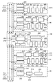
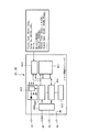
時計本体ケース16内には、図19に示すように、制御回路部163、制御プログラムを格納しているプログラムメモリ165、データを格納するデータメモリ166、時刻情報を生成する時計部167、及びバックアップ電池168が設けられているとともに、前記表示部161と前記キー操作部162とが時計本体ケース16の外周部に向かって設けられている。さらに、時計本体ケース16には、両リストバンド14、15の電源(Vcc)線411、511と接続する電源(Vcc)接続端子169、データ信号(Serial Data)線412、512と接続するデータ信号(Serial Data)接続端子170、クロック信号(Clock)線413、513と接続するクロック信号(Clock)接続端子171、及び接地(GND)線414、514と接続される接地(GND)接続端子172が設けられている。これら接続端子169〜172は、制御回路部163に接続されている。
【0066】
機能モジュール21、22には、電源インターフェース201、シリアルインターフェース202、及びメモリ203が設けられている。電源インターフェース201は、電源(Vcc)線411と接地(GND)線414とに接続されており、シリアルインターフェース202は、データ信号(Serial Data)線412とクロック信号(Clock)線413とに接続されている。
【0067】
機能モジュール23は、同様に接続された電源インターフェース201とシリアルインターフェース202を有するとともに、通信制御部204、モデム部205、送受信部206、及びアンテナ207を有している。
【0068】
機能モジュール24には、電源インターフェース201、シリアルインターフェース202、A/D変換器290、前記タッチパネル291が設けられている。電源インターフェース201は、電源(Vcc)線511と接地(GND)線514とに接続されており、シリアルインターフェース202は、データ信号(Serial Data)線512とクロック信号(Clock)線513とに接続されている。
【0069】
音声入出力・モジュール25は、同様に接続された電源インターフェース201とシリアルインターフェース202を有するとともに、音声コーディック208、アンプ209、及び前記スピーカ210とマイク211とを有している。
【0070】
電源モジュール26は、同様に接続された電源インターフェース201とシリアルインターフェース202を有するとともに、電圧安定化回路212、電池213、充電制御部214、及び充電端子215を有している。
以上の構成にかかる本実施の形態において、腕時計101は、図18(B)に示すように、時計部167で計時された現在時刻601、機能モジュール86によって撮像されたイメージ606を表示部1061に表示することができる。
【0071】
また、電源モジュール26の充電端子215を外部の電源に接続することにより、電池213を充電することができる。
【0072】
さらに、この電池213に充電された電力を、電源(Vcc)線411、511と電源(Vcc)接続端子169、及び接地(GND)線414、514と接地(GND)接続端子172にて、時計本体ケース16、機能モジュール21〜25に供給することができる。さらに、電池213が通常の動作電圧を下回った場合には、時計本体ケース16内のバックアップ電池168からの電力を、電源(Vcc)線411、511と電源(Vcc)接続端子169、及び接地(GND)線414、514と接地(GND)接続端子172にて、機能モジュール21〜25に供給することができる。
【0073】
そして、制御回路部163に音声認識機能を備えさせることにより、機能モジュール25により入力された音声情報に基づいて、制御回路部163は、腕時計本体11、機能モジュール21〜24、及び電源モジュール26をコントロールすることができる。
【0074】
例えば、制御回路部163が、機能モジュール25により入力された音声情報を認識して、無線モデム・モジュール23をコントロールすることにより、当該腕時計101を、音声認識機能付無線通信装置として使用することができる。
【0075】
(7)第2の実施の形態の変形例▲1▼
【0076】
図20は、第2の実施の形態の変形例を示すものであり、交換式の電池を用いたものである。時計本体ケース16とリストバンド14、15の接続構造、及び各機能モジュール21〜26の接続構造は、前述の第2の実施の形態と同様である。電源モジュール26は、交換式の電池219を着脱自在に内蔵しており、電池219は電圧安定化回路218、ダイオード217を介して電源(Vcc)接続端子169に接続され、ダイオード217と電源(Vcc)接続端子169間に、接地されたコンデンサ216が接続されている。さらに、電源モジュール26には、I/O制御回路部811、電源制御部812、モジュールID/シリアル番号等、当該機能モジュール固有の情報を記憶したROM816からなるモジュール制御部220が設けられている。I/O制御回路部811は、データ信号(Serial Data)接続端子170と、クロック信号(Clock)接続端子171とに接続されている。
【0077】
かかる変形例においても、電池219から供給された電力をバックアップ電池168に蓄えておくことができ、電池219の電力が消失しても、これを交換するまでの間、バックアップ電池168からの電力により、モジュール21〜25の動作を補償することができる。
【0078】
(8)第2の実施の形態の変形例▲2▼
【0079】
図21は、第2の実施の形態の変形例▲2▼を示すものであり、上述した調歩式(非同期式)ではなく、2線式シリアルバスで平衡型差動入出力方式を用いた場合における、時計本体ケース16の制御回路部163と各機能モジュール27とのシリアルバス接続の構成図である。
【0080】
2線式シリアルバスの平衡型差動入出力方式では、クロック信号(Clock)線413、513を使用しないものの、この代わりにデータ信号(Serial Data)線を2本に分け、制御回路部163からの送信(Tx)線416、516、受信(Rx)線417、517とすることにより、上述の調歩式(非同期式)よりもデータを高速に、送受信させることができる。
【0081】
尚、図示しないが、制御回路部163、及び機能モジュール27には、送信(Tx)線416、516、受信(Rx)線417、517にかかる回路構成が予め備えられているものとする。
【0082】
(9)第2の実施の形態の変形例▲3▼
【0083】
図22は、第2の実施の形態の変形例▲3▼を示すものであり、上述の平衡型差動入出力方式においてクロック信号(Clock)線413、513を加えた場合におけるリストバンド14、15の断面図(A)、及び、時計本体ケース16の制御回路部163と各機能モジュール28とのシリアルバス接続の構成図(B)である。
【0084】
図(A)において、リストバンド14、15の表面側には、電源(Vcc)線411、511、クロック信号(Clock)線413、513、制御回路部163からの送信(Tx)線416、516、受信(Rx)線417、517を備えさせ、人体に接触することによって接地する接地(GND)線414、514は、リストバンド14、15の裏面全面に設けられている。
【0085】
また機能モジュール28には、接続端子(電源(Vcc)線用)91、接続端子(クロック信号(Clock)線用)93、接続端子(接地(GND)線用)94、接続端子(送信(Tx)線用)96、及び接続端子(受信(Rx)線用)97が設けられている。
【0086】
したがって、上述の第2の実施の形態の変形例▲2▼に加え、クロック信号をも機能モジュールに送信出力できるので、よりスムーズにデータを送受信できるだけでなく、接地の問題においても良好なものとなる。
【0087】
尚、図示しないが、制御回路部163、及び機能モジュール28には、送信(Tx)線416、516、受信(Rx)線417、517にかかる回路構成が予め備えられているものとする。
【0088】
(10)第2の実施の形態の変形例▲4▼
【0089】
図23は、第2の実施の形態の変形例▲4▼を示すものであり、上述の平衡型差動入出力方式においてクロック信号(Clock)線413、513を加え、かつ、リストバンド14,15の両面に、電源(Vcc)線411、511、クロック信号(Clock)線413、513、制御回路部163からの送信(Tx)線416、516、及び受信(Rx)線417、517を備えさせ、接地(GND)線414、514を弾性を有する導電部材で構成し、リストバンドを構成する部材でサンドイッチさせた場合におけるリストバンド14、15の断面図である。
【0090】
このような構成によれば、上述の第2の実施の形態の変形例▲2▼に加え、リストバンド14、15の表裏両面に機能モジュール28を接続することができるとともに、接地(GND)線414、514を弾性を有する導電部材で構成することにより、より丈夫なリストバンド14、15を得ることができる。
【0091】
また、図23においては、機能モジュール28をリストバンド14、15の表裏面に接続する場合について述べたが、図24に示すように、クロック信号(Clock)線413、513を加え、かつ、リストバンド14,15の両面に、電源(Vcc)線411、511、クロック信号(Clock)線413、513、制御回路部163からの送信(Tx)線416、516、及び受信(Rx)線417、517の他に、送信Strobe(Txs)線418、518、受信Strobe(Rxs)線419、519、及び、予備データ(Rsv)線420、421、520、521をリストバンド14、15を備えさせ、接地(GND)線414、514を弾性を有する導電部材で構成してもよい。
【0092】
このような構成にすれば、制御回路部163と機能モジュール28との間で、大量の情報をスムーズに伝送することができる。
【0093】
また、伝送方式においても、半二重伝送、二重伝送によるデータの伝送が可能になる。
【0094】
なお、リストバンドにおける各信号線の配置は、これらの実施の形態、及び変形例に限定することはなく、リストバンドを構成する部材や、ユーザーの使用勝手に応じて任意に設計変更可能である。
【0095】
(11)第3の実施の形態
【0096】
図25は、本発明の第3の実施の形態にかかる腕時計31の外観図を示すものであり、(A)は腕時計31の全体図、(B)は表示部37の拡大図である。
【0097】
図12(A)に示すように腕時計31の構成は、リストバンド34、35にするデータ信号(Serial Data)線と電源(Vcc)線とを共用にして、接地(GND)線との2本のみを内装したものである。すなわち、この実施の形態にかかる腕時計31は、時計本体ケース36と、この時計本体ケース36の相対向する端部に取り付けられた一対のリストバンド34、35とを有している。一方のリストバンド34には、メモリ機能を有する機能モジュール300、301、緊急通報無線送信機機能を有する機能モジュール302が着脱自在に取り付けられており、他方のリストバンド35には、脈拍センサ機能を有する機能モジュール303、心電センサ機能を有する機能モジュール304、及び血糖センサ機能を有する機能モジュール305が着脱自在に取り付けられている。時計本体ケース36の上面には、LCDからなる表示部37が設けられており、側面には複数のキー操作部38が設けられている。
【0098】
両リストバンド34、35には、各々バス配線32、33が長手方向に沿って埋設されている。各バス配線32、33は、データ信号(Serial Data)線321、331と接地(GND)線322、332との2本で構成されており、データ信号(Serial Data)線321、331は、シリアル、アドレス、コマンド各データの入出力、及び電源(Vcc)線としての機能を兼ねるものである。
【0099】
また、図26に示すように、機能モジュール300〜305の各機能モジュール内蔵回路800は、データ接続端子306を介してデータ信号(Serial Data)線321、331に接続されているとともに、接地接続端子307を介して接地(GND)線322、332に接続されている。時計本体ケース36内には、制御回路部63、この制御回路部63に電力を供給する電池64が設けられているとともに、前記表示部37と前記キー操作部38とが時計本体ケース36の外周部に向かって設けられている。
【0100】
各機能モジュール300〜305は、図27に示すように、データ接続端子306が、電流源308、FET(Field-Effect Transistor:電界効果トランジスタ)309、インバータ310を介してシリアル制御部311に接続されているとともに、ダイオード318を介して電源制御部320に接続され、ダイオード318と電源制御部320の間には接地されたコンデンサ319が設けられている。シリアルバス制御部311は、コマンド/アドレスレジスタ312とデータレジスタ313とが接続され、データレジスタ313にはCRC生成部314が接続されている。コマンド/アドレスレジスタ312及びデータレジスタ313には、モジュールID/シリアル番号等、当該機能モジュール固有の情報を記憶したROM315、メモリ316、I/O回路317が接続されている。
【0101】
以上の構成にかかる本実施の形態において、データ信号(Serial Data)線321、331は、第1の実施の形態における電源(Vcc)線411、511と同様に電源を供給するように作用し、電源電位となっている。したがって、機能モジュール300〜305は送受信を行わない時は充電状態にあり、制御回路部63と機能モジュール300〜305との間で送受信を行う時には、負方向パルスの時間間隔の組み合わせによる、モールス符号のような信号が送受信される。
【0102】
詳細には、まず、時計本体ケース36の制御回路部63から一定時間のリセットパルスを送信して、機能モジュール300〜305との通信を開始し、それを受けた機能モジュール300〜305では、確認応答信号を返す。それを受けて時計本体ケース36の制御回路部63は、コマンド、モジュールID、及びデータ送信の場合はアドレス信号に続けてシリアル伝送で送信し、通信終了符号として再びリセット信号を送信する。したがって、このように信号の送受信を行うことにより、リストバンド34、35にデータ信号(Serial Data)線321、331と接地(GND)線322、332との2本のバス配線を配設するのみで、機能モジュール300〜305の制御が可能となり、結果、腕時計31は、。図25(B)に示すようにセンサ機能を有する機能モジュール303〜305によって装着者から検出した各種生体情報データを表示することができる。尚、図25(B)においては、制御回路部63で計時された現在時刻601、心拍数608、最高/最低血圧608、脈拍609が表示されている。また、これらの計測結果をメモリ機能を有する機能モジュール300、301に記憶させたりすることもできる。
【0103】
また、各種生体情報データにおいて異常値を検出したり、予め定められた一定値を超えた場合は、緊急通報無線送信機機能を有する機能モジュール302により、予めメモリに記憶した通報先や救急センターへ自動的に緊急通報することもできる。よって、各種生体情報データの計測モニターとして、医療健康管理、在宅介護、セキュリティ用途などとして利用することができる。
【0104】
(12)第3の実施の形態の変形例▲1▼
【0105】
図28は、本発明の第3の実施の形態▲1▼を示すものであり、機能モジュール300〜305にコンデンサやキャパシタからなる寄生電源を設けるようにしたものである。すなわち、時計本体ケース36内には、前述と同様の表示部37、キー操作部38、電池64が設けられているとともに、シリアルバス制御部340、制御回路部341、メモリ342が設けられている。シリアルバス制御部340は、インバータ343、344を介してデータ信号(Serial Data)線321、331に接続され、その間に電源(+Vcc)に一端を接続された抵抗345の他端が接続されている。
【0106】
メモリ機能を有する機能モジュール300、301には、図27と同様に、電流源308からI/O回路317までの各部が設けられているとともに、電源制御部320に代わってコンデンサやキャパシタからなる寄生電源346が設けられている。センサ機能を有する機能モジュール303〜305には、同様に、電流源308からI/O回路など317までの各部及び寄生電源346が設けられているとともに、センサデータメモリ347、A/D変換器348、アンプ349、センサ350が設けられている。
【0107】
かかる本例においては、時計本体ケース36内の電池64からの電力が電源(Vcc)線411、511を介して各機能モジュール300、301、303〜305に供給され、寄生電源346に充電される。よって、各機能モジュール300、301、303〜305は、寄生電源346からの電力により動作することができ、前述と同様に、負方向パルスの時間間隔の組み合わせからなる信号により、時計本体ケース36側と各機能モジュール300、301、303〜30とでデータの送受信を行うこともできる。
【0108】
(13)第3の実施の形態の変形例▲2▼
【0109】
図29は、第3の実施の形態の変形例▲2▼を示すものである。時計本体ケース36には、各々一対の貫通孔691を有するバス接続用レセプタクル69が設けられている。また、時計本体ケース36に配置された制御回路部63には、相対向する端部に各々一対ずつ板バネからなる本体接続端子351が設けられている。一方、両リストバンド34、35の端部には、各々データ信号(Serial Data)線321、331と接地(GND)線322、332とに接続された接続用プラグ352が設けられている。前記貫通孔691の内周面、及び時計本体ケース6と時計バックケース66との間の全周に亙って、防水パッキング71が介装されている。そして、両リストバンド34、35の端部は、接続用プラグ352をバス接続用レセプタクル69の貫通孔691に挿入した状態で、固定用ビス67によりバス接続用レセプタクル69に固定されている。これにより、本体接続用プラグ352が本体接続端子351に弾接して、データ信号(Serial Data)線321、331と接地(GND)線322、332が接続プラグ352及び本体接続端子351を介して、制御回路部63に接続される。本例によれば、防水パッキング71により浸水に伴う接触不良等を防止することができる。
【0110】
(14)第3の実施の形態の変形例▲3▼
【0111】
図30は、第3の実施の形態の変形例▲3▼を示すものである。前記バス接続用レセプタクル69に設けられた各貫通孔691には、コイルスプリング692が嵌挿され、さらにコイルスプリング692に断面略T字型の押しボタン型端子693が嵌挿されている。そして、両リストバンド34、35端部は、押しボタン型端子693の頭部に接続用プラグ352を圧接させた状態で、固定用ビス67によりバス接続用レセプタクル69に固定されている。これにより、コイルスプリング692が収縮して、押しボタン型端子693が本体接続端子351に弾接し、データ信号(Serial Data)線321、331と接地(GND)線322、332が接続プラグ352、押しボタン型端子693及び本体接続端子351を介して、制御回路部63に接続される。本例によれば、本体接続端子351のバネ力とコイルスプリング692のバネ力とにより、接触状態が維持されることから衝撃に対して強く、この腕時計31が所謂アウトドア用であっても、適正に接触状態を維持することができる。
【0112】
(15)第3の実施の形態の変形例▲4▼
【0113】
図31は、第3の実施の形態の変形例▲4▼を示すものであり、(A)は前記リストバンド34、35の裏面側にデータ信号(Serial Data)線321、331と接地(GND)線322、332が配置され、機能モジュール300〜305は、断面略コ字状であってリストバンド34、35を抱持する形状になっており、データ信号(Serial Data)線321、331、接地(GND)線322、332と接触する箇所には、接続端子306、307が設けられている。
【0114】
したがってこのような接続構造にすることにより、機能モジュール300〜305は確実にリストバンド34、35に保持され、かつ、データ信号(Serial Data)線321、331、接地(GND)線322、332が接続端子306、307と接触して確実な導通性が得られる。
【0115】
また、(B)においては機能モジュール300〜305がリストバンド34、35の周囲を囲うような構造になっており、更にリストバンド34、35のデータ信号(Serial Data)線321、331、接地(GND)線322、332と接続端子306、307と接触する部分はバネ性を有する構造になっている。
【0116】
したがって、上記(A)の場合と比較して、更に確実な保持と導通性が得られる。またこの他にリストバンド34、35の表面側にデータ信号(Serial Data)線321、331、接地(GND)線322、332を備え、機能モジュール300〜305をリストバンド34、35の側面部で保持する構造(図31(C))、リストバンド34、35の側面部にデータ信号(Serial Data)線321、331、接地(GND)線322、332を備えると同時に、この側面部で機能モジュール300〜305を保持する構造(図31(D))、及びリストバンド34、35の表面全面にデータ信号(Serial Data)線321、331、裏面全面に接地(GND)線322、332を備えさせ、コの字形状に形成された機能モジュール300〜305を挟み込む構造(図31(E))があり、このような接続構造によりリストバンド34、35のデータ信号(Serial Data)線321、331、及び接地(GND)線322、332と機能モジュール300〜305の接続端子306、307との確実な導通性と機能モジュール300〜305の確実な保持とが実現可能である。
【0117】
(16)第3の実施の形態の変形例▲5▼
【0118】
図32は、本発明の第3の実施の形態の変形例▲5▼を示すものであり、リストバンドを構成する駒に機能モジュールを設けたものである。すなわち、時計本体ケース36内の回路構成は、図26に示したものと同様であって、表示部37、キー操作部38、制御回路部63、電池64で構成されている。時計本体ケース36の両端部には、制御回路部63に接続されたデータ信号端子631と、制御回路部63及び電源64に接続されるとともに接地された接地端子632とが設けられている。
【0119】
一方、時計本体ケース36の両端部に接続されたリストバンド44、45は、複数の駒401を順次バネ棒402により着脱自在に連結してなり、機能モジュール403は、駒401とその内部に配置された機能モジュール内蔵回路800とから構成されている。この駒401と一体的に設けられた機能モジュール403には、図33に示すように、データ信号線(Serial Data)431と接地(GND)線432とが設けられている。データ信号線431(Serial Data)の両端部は、駒401の両端部に設けられたデータ信号凸端子3311とデータ信号凹端子3312に接続され、接地(GND)線432の両端部は接地凸端子4321と接地凹端子3322に接続されている。
【0120】
また、データ信号(Serial Data)線431には、電流源308、FET309、インバータ310を介してシリアル制御部311に接続されているとともに、ダイオード318を介して電源制御部320に接続され、ダイオード318と電源制御部320の間には接地されたコンデンサ319が設けられている。シリアル制御部311には、CRC生成部314、モジュールID/シリアル番号等、当該機能モジュール固有の情報を記憶したROM315、メモリ316、I/O回路317が接続されている。また、接地(GND)線432は、電流源308及びFET309に接続されているとともに、接地されている。
【0121】
なお、機能モジュール内蔵回路800が設けられていない駒、つまり機能モジュール403ではない駒401には、データ信号(Serial Data)線431と接地(GND)線432、データ信号凸端子4311とデータ信号凹端子4312、及び接地凸端子4321と接地凹端子4322のみが設けられている。
【0122】
そして、端部の駒401をバネ棒402より時計本体ケース36に接続させると、該時計本体ケース36のデータ信号端子631と接地端子632とに、駒401のデータ信号凸端子4311と接地凸端子4321とが接触する。さらに、順次バネ棒402により駒401を接続させると、前側の駒401のデータ信号凹端子4312と接地凹端子4322に、後側の駒401のデータ信号凸端子4311と接地凸端子4321とが接触する。これにより、各駒401に配置されたデータ信号線431と接地線432との接続状態が形成されるとともに、さらに時計本体ケース36との接続状態が形成される。
【0123】
したがって、この変形例においても、第3の実施の形態と同様に、リストバンド44、45にデータ信号(Serial Data)線431と接地(GND)線432との2本のバス配線を配設するのみで、機能モジュール403の制御が可能となる。しかも、この変形例においては、リストバンド44、45を構成する駒401自体が機能モジュール403であることから、リストバンド44、45からの突出が皆無であって、一般的な腕時計と同様の感覚で携帯することができる。
【0124】
(17)第4の実施の形態
【0125】
上述の第1〜第3の実施の形態においては、リストバンドにバス配線を設けて、このバス配線により腕時計本体と機能モジュールとを電気的に接続するようにしたが、時計本体とリストバンドに装着された機能モジュール間をBluetooth等の近接無線によりデータ通信させるようにしてもよい。以下、このような場合を適用した詳細な説明を本発明の第4の実施の形態を図に従って説明する。本発明の第3の実施の形態にかかる腕時計100の外観図を示すものであり、(A)は腕時計100の全体図、(B)は表示部1061の拡大図である。
【0126】
図の説明において上述の第1〜第3の実施の形態で説明した構成は、基本的に同じ構造であるので、説明を省略する。
【0127】
図34に示すように、本発明の第4の実施の形態にかかる腕時計100は、時計本体ケース106と、この時計本体ケース106の相対向する端部に取り付けられた一対の樹脂製のリストバンド104、105とを有している。一方のリストバンド104には、メモリ機能を有する機能モジュール1071、撮像機能を有する機能モジュール86が着脱自在に取り付けられており、他方のリストバンド105には、音声入出力機能を有する機能モジュール25、及び電源モジュール26が着脱自在に取り付けられている。時計本体ケース106の上面には、LCDからなる表示部1061が設けられているとともに、複数のキー操作部1062が設けられている。
【0128】
両リストバンド104、105には、各々バス配線として、電源(Vcc)線411、511、及び接地(GND)線414、514が長手方向に配置されている。なお、時計本体ケース16とリストバンド14、15の接続配置構造は、図29及び図30に示した第3の実施の形態と同様である。
【0129】
時計本体ケース106内には、図35に示すように、制御回路部1063、制御プログラムを格納しているプログラムメモリ858、データを格納するデータメモリ817、時刻情報を生成する時計部167、及びバックアップ電池168が設けられているとともに、前記表示部1061と前記キー操作部1062とが時計本体ケース106の外周部に向かって配置される。さらに、時計本体ケース106には、両リストバンド104、105の電源(Vcc)線411、511と接続する電源(Vcc)接続端子169、及び接地(GND)線414、514と接続される接地(GND)接続端子172が設けられている。これら接続端子169、172は、制御回路部1063に接続されている。
【0130】
機能モジュール1071には、電源インターフェース201、モジュールID/シリアル番号等、当該機能モジュール固有の情報を記憶したROM816、及びメモリ203が設けられている。電源インターフェース201は、電源(Vcc)線411と接地(GND)線414とに接続されている。これら電源インターフェース201、ROM816、及びメモリ203は、制御回路部856を介して、符号/復号部852、変復調部853、送受信部854、及びアンテナ855に順次接続されている。
【0131】
撮像機能を有する機能モジュール86は、同様に電源インターフェース201、モジュールID/シリアル番号等、当該機能モジュール固有の情報を記憶したROM816を有するとともに、画像データメモリ857、制御回路部856、符号/復号部852、変復調部853、送受信部854、及びアンテナ855を有している。さらに、機能モジュール86は、信号処理部8622、A/D変換器8621、CCDからなる入力デバイス864、及び撮像レンズ865を有している。
【0132】
機能モジュール25は、同様に接続された電源インターフェース201及びモジュールID/シリアル番号等、当該機能モジュール固有の情報を記憶したROM816を有するとともに、音声信号処理部2501、音声コーディック208、アンプ209、及び前記スピーカ210とマイク211とを有している。さらに、音声入出力・モジュール25は、制御回路部861、符号/復号部852、変復調部853、送受信部854、及びアンテナ855を有している。
【0133】
電源モジュール26は、同様に接続された電源インターフェース201を有するとともに、電圧安定化回路212、充電制御部214、充電端子215及び電池213を有している。
【0134】
以上の構成にかかる本実施の形態において、電源モジュール26の充電端子215を外部の電源に接続することにより、電池213を充電することができる。また、この電池213に充電された電力を、電源(Vcc)線411、511と電源(Vcc)接続端子169、及び接地(GND)線414、514と接地(GND)接続端子172にて、時計本体ケース106、機能モジュール1071、撮像機能を有する機能モジュール86、機能モジュール25に供給することができる。また、腕時計100は、図34(B)に示すように、制御回路部167で計時された現在時刻601、機能モジュール86によって撮像されたイメージ610を表示部1061に表示することができる。
【0135】
さらに、電池213が通常の動作電圧を下回った場合には、時計本体ケース106内のバックアップ電池168からの電力を、電源(Vcc)線411、511と電源(Vcc)接続端子169、及び接地(GND)線414、514と接地(GND)接続端子172にて、機能モジュール1071、撮像機能を有する機能モジュール86、機能モジュール25に供給することができる。
【0136】
(18)第5の実施の形態
上述の第1〜第3の実施の形態においては、リストバンドにバス配線を設けて、このバス配線により腕時計本体と機能モジュールとを電気的に接続するようにしたが、時計本体とリストバンドに装着された機能モジュール間を赤外線通信により接続させるようにしてもよい。以下、このような場合を適用した詳細な説明を本発明の第5の実施の形態を図に従って説明する。尚、図の説明において上述の第1〜第3の実施の形態で説明した構成は、基本的に同じ構造であるので、説明を省略する。
【0137】
すなわち、図36(A)に示すように、腕時計110の時計本体ケース116内には、制御回路部63、電源64、赤外線によるデータ送受信用の送受信制御部1165が設けられているとともに、上記第4の実施の形態と同様に表示部1061と前記キー操作部1062とが時計本体ケース116の外周部に向かって配置される。また、リストバンド4、5は、上記第2の実施の形態の変形例▲3▼と同様のバス配線を有し、各機能モジュール1180〜1184の赤外線入力部1185に対向する位置に接続端子((Tx)線用)96に代えて、赤外線発光デバイスを備える発光部196、そして、赤外線出力部1186に対向する位置に接続端子((Rx)線用)97に代えて、赤外線受光デバイスを備える受光部197が設けられている。また発光部196は、送信(Tx)線416、516に接続され、受光部197は、受信(Rx)線417、517に接続されている。
【0138】
一方、各モジュール1180〜1183は、電源(Vcc)線411、511と接地(GND)線414、514とに接続されているとともに、前記リストバンド4、5側の発光部196に対向する受光部1185、及び受光部197に対向する発光部1186を有している。
【0139】
同図(B)に示すように、機能モジュール1180は、接続端子91、94、及び前記受光部1185、発光部1186を有するとともに、電源制御部812、変復調部853、符号/復号部852、I/O制御回路部859、ROM816、メモリ817、周囲環境や生体情報を取得するためのセンサデバイス、撮像デバイス、及び音声出力デバイス等、各種デバイスとのデータ送受信を制御するI/O回路など860、及びCRC生成部815を有している。したがって、これらの機能モジュール1180〜1183によれば、受光部1185、発光部1186、及びリストバンド4、5側の発光部196、受光部197を介して、時計本体ケース116側と赤外線通信によるデータの授受が可能となる。
【0140】
(19)第6の実施の形態
図37は、本発明の第6の実施の形態を示すものであり、電磁誘導による誘導電磁界を用いてリストバンド内のアンテナコイルと各モジュール内蔵のアンテナコイルとの間でデータを非接触で送受信するようにしたものである。すなわち、図37(A)に示すように、腕時計120の時計本体ケース126内には、制御回路部63、電源64が設けられているとともに、上記第4の実施の形態と同様に表示部1061と前記キー操作部1062とが時計本体ケース126の外周部に向かって配置される。制御回路部63は送受信制御部1266を介して、リストバンド104、105内に配置されたリストバンド側アンテナコイル2041、2051に接続されている。
【0141】
前記送受信部1266には、図37(B)に示すように、復調回路661、フィルター&増幅回路662、復号回路663、アンテナ駆動回路664、発振回路665、変調回路667、符号化回路666が設けられている。そして、復号回路663及び符号化回路666は制御回路部63に接続され、発振回路665は時刻情報を生成する時計部167を介して、制御回路部63に接続されている。さらに、制御回路部63には、前記キー操作部1062、表示部1061が接続されているとともに、データメモリ166、バックアップ電池168が接続されている。
【0142】
他方、機能モジュール1280〜1283は、適宜の装着手段により、リストバンド104、105に脱着可能に取り付けられている。各モジュール1280〜1284は、モジュール側アンテナコイル1286を有するとともに、復調回路353、復号回路354、クロック再生回路359、整流機能も備えるA/D変換器358、寄生電源346、符号化回路356、変調回路357、制御回路部856、ROM816、メモリ817、入出力デバイス884を有している。したがって、この実施の形態によれば、リストバンド側アンテナコイル2041、2051と各機能モジュール1280〜1283内のモジュール側アンテナコイル1286との間の電磁誘導により、各機能モジュール1280〜1283とのデータの送受信ができるだけでなく、電池64の電源電力も非接触で各機能モジュール1280〜1283へ供給できるので、有線のバス配線を設ける必要がなく、配線構造を簡単化することができる。
【0143】
(20)第7の実施の形態
【0144】
図38は、本発明の第7の実施の形態を示すものであり、機能モジュールをコイン型にして、リストバンドに脱着自在に嵌着するようにしたものである。以下、本発明の第7の実施の形態を図に従って説明する。尚、図の説明において上述の第1〜第3の実施の形態で説明した構成は、基本的に同じ構造であるので、説明を省略する。
【0145】
すなわち、時計本体ケース36の両端部に係着されたリストバンド134、135には、平面視において円形であって、機能モジュール1300〜1303を脱着自在に嵌合可能な複数の機能モジュール嵌め込み孔1341、1351が形成されている。モジュール嵌め込み孔1341、1351の底面には、電源(Vcc)線511、データ信号(Serial Data)線512、クロック信号(Clock)線513、接地(GND)線514の一部が露出している。他方、機能モジュール1300〜1303の下面には、前記各線511〜514の露出した部分に対応する部位に、接続端子91〜94が設けられている。
【0146】
したがって、この実施の形態によれば、必要に応じて機能モジュール1300〜1302をモジュール嵌め込み孔1341、1351に嵌着することにより、容易に機能付加を行うことができる。
【0147】
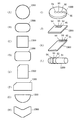
(21)第7の実施の形態の変形例
上述の第7の実施の形態においては、機能モジュール1300を平面視において円形としたが、図39に示すように、楕円形(B)、正方形(C)、角部を湾曲にした長方形(D)、特定の角部を切欠した矩形(E)(F)、半円形(G)、略くの字形(H)等、平面視円形に限ることなく適宜の形状としてもよい。また、接続端子91〜94の形成部位に関しても、一側部に変位させて設けたり(I)、一辺側に変位させて設けてもよく(J)(K)、また、機能モジュール1300が円筒形である場合にはその周面に設けるようにしてもよい(L)。
【0148】
(22)第8の実施の形態及びその変形例
【0149】
第8の実施形態は、上記第1の実施の形態において、時計本体ケース5006(6)に内蔵される制御回路部63と各機能モジュール80〜84との間でデータの送受信を行う場合、その制御処理を詳述するものであり、図の説明において第1の実施の形態で説明した構成は、基本的に同じ構造であるので、説明を省略する。
【0150】
第8の実施の形態において、図40に示すように、腕時計5001における時計本体ケース5006は上記第1の実施の形態で説明した構成に加え、後述する機能モジュール制御データメモリ1661を内蔵している。
【0151】
図41は、各機能モジュール80〜84の回路構成図であり、図の説明において第1の実施の形態で説明した構成は、基本的に同じ構造であるので、説明を省略する。I/O制御回路部1811は、電源制御部812の電源管理を行う。
【0152】
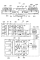
ROM1816には、図41に示すように、当該機能モジュールを製造したメーカーや、メーカーにおける型番等を示すメーカー/シリーズ符号(Family Code)8160、製造シリアル番号(Serial No.)8161、当該機能モジュールが電源モジュール若しくは電源を含んでいるか否かを1bitデータ(フラグ)情報で設定した電源/電池モジュールビット(PS)8162、当該機能モジュールが外部からのデータを読み込めるか否かを1bitデータ(フラグ)情報で設定した入力(データ読込可)モジュールビット(IN)8163、当該機能モジュールが外部へデータを書き出せるか否かを1bitデータ(フラグ)情報で設定した出力(データ書出可)モジュールビット(OUT)8164、表示フォーマット設定データ(DF)8165、モジュール種別コード(Module Code)8166、モジュール仕様コード(Module Spec)8167、消費電力情報データ8168(PCI: Power Consumption Information)、及びエラーチェック(CRC巡回訂正符号)8169が格納されている。またこれらのデータのうち、モジュール種別コード(Module Code)8166、モジュール仕様コード(Module Spec)8167は、機能モジュール制御データメモリ1661に格納されている後述する各テーブルによって予め定義されている。
【0153】
表示フォーマット設定データ(DF)8165は、腕時計5001の表示部60に当該機能モジュールに関する事項を表示する際、その表示フォーマットを規定するデータであり、消費電力情報データ(PCI)8168は当該機能モジュールが正常に動作するために必要な消費電力に関するデータ(Off時/On時平均/On時Max等)である。また、モジュール種別コード(Module Code)8166は、当該機能モジュールの種別を示す符号であり、モジュール仕様コード(Module Spec)8167は当該機能モジュールの仕様を示す符号である。これら、モジュール種別コード8166とモジュール仕様コード8167の詳細については、後述する。 尚、これらのデータ、及びコードを各機能モジュールと時計本体とで送受信する場合のデータの構成は、図10、及び図11に準じるものであるが、各データ及びコードについては、変更される。
【0154】
図42は、一例として前記機能モジュール82、83の詳細を示す回路構成図である。この機能モジュール82、83のROM1816には、前記図41に示した当該機能モジュールのメーカー/シリーズ符号8160からエラーチェック(CRC巡回訂正符号)8169までの情報が格納されている。これら情報8160〜8169において、機能モジュール82、83のモジュール種別コード8166は、同図の右側に「Module Code=0100(=センサ系(測定処理)」と定義されている。また、機能モジュール83のモジュール仕様コード8167は、「Module Spec=0010(気圧計(hPa)」として定義されている。
【0155】
図43は、本発明の第8の実施の形態における変形例を示すものであり、上記第2の実施の形態において、時計本体ケース5016(6)に内蔵される制御回路部163と各機能モジュール21〜26との間でデータの送受信を行う場合、その制御処理を詳述するものであり、図の説明において第2の実施の形態で説明した構成は、基本的に同じ構造であるので、説明を省略する。
【0156】
第8の実施の形態の変形例において、図43に示すように、腕時計5002における時計本体ケース5016は上記第1の実施の形態で説明した構成に加え、後述する機能モジュール制御データメモリ1661を内蔵している。
【0157】
機能モジュール21〜26は、それえぞれ電源(Vcc)線411、511、データ信号(Serial Data)線412、512、クロック信号(Clock)線413、513、接地(GND)線414、514とに接続されている。
【0158】
図44は、機能モジュール21、22の詳細を示す回路構成図であり、図の説明において第2の実施の形態で説明した構成は、基本的に同じ構造であるので、説明を省略する。
【0159】
ROM1817には、前記図41に示したものと同様に、当該機能モジュールのメーカー/シリーズ符号8160からエラーチェック(CRC巡回訂正符号)8169までの情報が記憶されている。これら8160〜8169において、機能モジュール21、22のモジュール種別コード8166は、メモリ機能を有するものであり、「Module Code=0010(=メモリ系)」として定義されている。又、機能モジュール21のモジュール仕様コード8167は、「Module Spec=0110(=32MB/Flash)」として定義されている。
【0160】
図45は、前記機能モジュール23の詳細を示す回路構成図であり、第2の実施の形態で説明した構成は、基本的に同じ構造であるので、説明を省略する。
【0161】
ROM1818には、前記図41に示したものと同様に当該機能モジュール23のメーカー/シリーズ符号8160からエラーチェック(CRC巡回訂正符号)8169までの情報が記憶されている。これら8160〜8169において、機能モジュール23のモジュール種別コード8166は、「Module Code=0111(=無線処理系(通信方式)系)」として定義されている。また、この機能モジュール23のモジュール仕様コード8167は、「Module Spec=0101(近接無線通信(Bluetooth))」として定義されている。
【0162】
図46は、前記機能モジュール24の詳細を示す回路構成図であり、第2の実施の形態で説明した構成は、基本的に同じ構造であるので、説明を省略する。
【0163】
ROM1819には、前記図41のものと同様に当該機能モジュール24のメーカー/シリーズ符号8160からエラーチェック(CRC巡回訂正符号)8169までの情報が記憶されている。これら8160〜8169において、機能モジュール24のモジュール種別コード8166は、「Module Code=0101(=入力処理系(デバイス))」として定義されている。特にこの機能モジュール24がデジタルカメラである場合は、モジュール仕様コード8167は、「Module Spec=0111(=イメージインプット(CCD、CMOS))」として定義されている。
【0164】
図47は、前記機能モジュール25の詳細を示す回路構成図であり、第2の実施の形態で説明した構成は、基本的に同じ構造であるので、説明を省略する。
【0165】
ROM1820には、前記図41のものと同様に当該機能モジュール25のメーカー/シリーズ符号8160からエラーチェック(CRC巡回訂正符号)8169までの情報が記憶されている。これら8160〜8169において、当該機能モジュール25のモジュール種別コード8166は、「Module Code=0110(=出力処理系(デバイス)」として定義されている。また、モジュール仕様コード8167は、「Module Spec=0101(オーディオ出力(スピーカ、イヤホン))」として定義されている。
【0166】
図48は、前記電源モジュール26の詳細を示す回路構成図であり、第2の実施の形態で説明した構成は、基本的に同じ構造であるので、説明を省略する。
【0167】
ROM1821には、前記図41のものと同様に当該電源モジュール26のメーカー/シリーズ符号8160からエラーチェック(CRC巡回訂正符号)8169までの情報が記憶されている。これら8160〜8169において、この電源モジュール26のモジュール種別コード8166は、「Module Code=1101(=二次電池)」として定義されている。また、この電源モジュール26のモジュール仕様コード8167は、「Module Spec=0101(=3.6V、200mAh)」として定義されている。
【0168】
図49〜図58は、各腕時計5001、5002に設けられている前記モジュール制御データメモリ1661に記憶されているテーブル1662〜1671を示すものである。各テーブル1662〜1671には、モジュール識別コードと、モジュール仕様コード、及び機能が対応して記憶されている。
【0169】
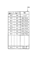
図49は、時間計測系機能モジュールテーブル1662であり、モジュール識別コードは、サーフィンタイマー、ヨットタイマー、・・・等の、時間計測系機能モジュールに全て共通して「0000」が対応付けて記憶されている。また、モジュール仕様コードは当該機能モジュールの機能に応じて相互に異なる。したがって、腕時計5001、5002の制御回路部63、163は、この時間計測系機能モジュールテーブル1662を参照することにより、リストバンド4、5に嵌合して接続された機能モジュールが時間計測機能を備えるものであるか否か、また、時間計測機能を備えるものであった場合、どのような仕様であるのかをモジュール仕様コードで判別することができる。
【0170】
図50は、CPU/演算処理プログラム系機能モジュールテーブル1663であり、モジュール識別コードは、日出/日入演算、月齢演算・・・等の、CPU/演算処理プログラム系機能モジュールに全て共通の「0001」が対応付けて記憶されている。また、モジュール仕様コードは当該機能モジュールの機能に応じて相互に異なる。したがって、腕時計5001、5002の制御回路部63、163は、このCPU/演算処理プログラム系機能モジュールテーブル1663を参照することにより、リストバンド4、5に嵌合して接続された機能モジュールがCPU/演算処理機能を備えるものであるか否か、また、CPU/演算処理機能を備えるものであった場合、どのような仕様であるのかをモジュール仕様コードで判別することができる。
【0171】
図51は、メモリ系機能モジュールテーブル1664であり、モジュール識別コードは、1MB/SRAM、2MB/SRAM、・・・等の、メモリ系機能モジュールに全て共通の「0010」が対応付けて記憶されている。また、モジュール仕様コードは当該機能モジュールのメモリ容量、及びハードウェアの仕様に応じて異なる。したがって、腕時計5001、5002の制御回路部63、163は、このメモリ系機能モジュールテーブル1664を参照することにより、リストバンド4、5に嵌合して接続された機能モジュールがメモリ機能を備えるものであるか否か、また、メモリ機能を備えるものであった場合、どのような容量、ハードウェアで構成されているかをモジュール仕様コードで判別することができる。
【0172】
図52は、データバンク系機能モジュールテーブル1665であり、モジュール識別コードは、アドレス帳、スケジュール帳・・・等の、データバンク系機能モジュールに全て共通の「0011」が対応付けて記憶されている。また、モジュール仕様コードは当該機能モジュールの機能に応じて相互に異なる。したがって、腕時計5001、5002の制御回路部63、163は、このデータバンク系機能モジュールテーブル1665を参照することにより、リストバンド4、5に嵌合して接続された機能モジュールがデータバンク機能を備えるものであるか否か、また、データバンク機能を備えるものであった場合、どのような仕様であるのかをモジュール仕様コードで判別することができる。
【0173】
図53は、センサ系機能モジュールテーブル1666であり、モジュール識別コードは、温度計、気圧計・・・等の、センサ系機能モジュールに全て共通の「0100」が対応付けて記憶されている。また、モジュール仕様コードは当該機能モジュールの機能に応じて相互に異なる。したがって、腕時計5001、5002の制御回路部63、163は、このセンサ系機能モジュールテーブル1666を参照することにより、リストバンド4、5に嵌合して接続された機能モジュールがセンサ機能を備えるものであるか否か、また、センサ機能を備えるものであった場合、どのような仕様であるのかをモジュール仕様コードで判別することができる。
【0174】
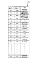
図54は、入力処理系(デバイス)機能モジュールテーブル1667であり、モジュール識別コードは、コネクタ経由インプット、キーインプット、・・・等の、入力処理系機能モジュールに全て共通の「0101」が対応付けて記憶されている。また、モジュール仕様コードは当該機能モジュールの機能に応じて相互に異なる。したがって、腕時計5001、5002の制御回路部63、163は、この入力処理系(デバイス)機能モジュールテーブル1667を参照することにより、リストバンド4、5に嵌合して接続された機能モジュールが入力デバイスを備えるものであるか否か、また、入力デバイスを備えるものであった場合、どのような入力デバイスであるのかをモジュール仕様コードで判別することができる。
【0175】
図55は、出力処理系(デバイス)機能モジュールテーブル1668であり、モジュール識別コードは、コネクタ経由アウトプット、表示出力、・・・等の、出力処理系機能モジュールに全て共通の「0110」が対応付けて記憶されている。また、モジュール仕様コードは当該機能モジュールの機能に応じて相互に異なる。したがって、腕時計5001、5002の制御回路部63、163は、この出力処理系(デバイス)機能モジュールテーブル1668を参照することにより、リストバンド4、5に嵌合して接続された機能モジュールが出力デバイスを備えるものであるか否か、また、出力デバイスを備えるものであった場合、どのような出力デバイスであるのかをモジュール識別コードで判別することができる。
【0176】
図56は、無線処理系(通信方式)機能モジュールテーブル1669であり、モジュール識別コードは、無線通信一般、無線受信一般、・・・等の、無線処理系機能モジュールに全て共通の「0111」が対応付けて記憶されている。また、モジュール仕様コードは当該機能モジュールの機能に応じて相互に異なる。したがって、腕時計5001、5002の制御回路部63、163は、この無線処理系(通信方式)機能モジュールテーブル1669を参照することにより、リストバンド4、5に嵌合して接続された機能モジュールが無線処理機能を備えるものであるか否か、また、無線処理機能を備えるものであった場合、どのような機能を備えるものであるのかを判別することができる。
【0177】
図57及び図58は、一次電池系及び二次電池系機能モジュールテーブル1670、1671であり、モジュール識別コードは、1.5V,80mAh、3V,150mAh、・・・等の、各電池系機能モジュール全て「1000」(一次電池)、「1101」(二次電池)が対応付けて記憶されている。また、モジュール仕様コードは当該モジュールの能力に応じて相互に異なる。したがって、腕時計5001、5002の制御回路部63、163は、この一次電池系及び二次電池系機能モジュールテーブル1670、1671を参照することにより、リストバンド4、5に嵌合して接続された機能モジュールが各電源を有するか否か、また、電源を有している場合、どのような機能を備えるものであるのかを判別することができる。
【0178】
以上の構成にかかる第8の実施の形態及びその変形例において、各腕時計5001、5002の制御回路部63、163は、内部に記憶されている処理プログラムに基づき、先ず図59に示すフローチャートに従って処理を実行する。すなわち、リストバンド4、5に嵌合して新規に接続された機能モジュールがあるか否かを判断する(ステップS1)。新規に接続された機能モジュールがある場合には、当該機能モジュールの前記ROM816、1816〜1821に記憶されている8160〜8169のうち、モジュールID(メーカー/シリーズ符号8160、製造シリアル番号8161)を読み込んで、当該腕時計5001、5002に対応するものか否かチェックするとともに(ステップS2)、後続するモジュール情報(電源/電池モジュールビット(PS)8162、入力(データ読込可)モジュールビット(IN)8163、出力(データ書出可)モジュールビット(OUT)8164、表示フォーマット設定データ(DF)8165、モジュール種別コード(Module Code)8166、モジュール仕様コード(Module Spec)8167、消費電力情報データ8168(PCI: Power Consumption Information)、及びエラーチェック(CRC巡回訂正符号)8169)を読み込む(ステップS3)。
【0179】
さらに、ステップS2で読み込んだモジュールIDと対応させて、ステップS3で読み込んだモジュール情報をモジュール制御データメモリ1661内に登録する(ステップS4)。次いで、接続されている機能モジュールのアイコン及びモジュール情報を表示部60、161に表示する(ステップS5)。このステップS5での処理により、前記各腕時計5001、5002の表示部60、161は、図60に例示するように、接続されている機能モジュールのアイコンやモジュール情報が表示され、あるいは図61に例示するようにモジュール情報がツリー状に表示される(図60において、610は出力処理系(デバイス)機能モジュールの音声出力アイコン、611は無線処理系(通信方式)機能モジュールのアイコン、612はメモリ機能モジュールアイコン、613は電源モジュールアイコンをそれぞれ示す。)。また、他にも新規に接続された機能モジュールがあるか否かを判断し(ステップS6)、新規に接続された機能モジュールに対し、ステップS2〜S5の処理を繰り返す。
【0180】
そして、新規に接続された全ての機能モジュールに対し、ステップS2〜S5の処理を終了した場合、又はステップS1での判断の結果、新規に接続された機能モジュールがなかったと判断した場合は、逆にリストバンド4、5からはずされた機能モジュールがあるか否かを判断する(ステップS7)。はずされた機能モジュールがある場合には、前述のステップS4でモジュール制御データメモリ1661内に登録した当該機能モジュールのモジュールIDとモジュール情報とを登録データから削除する(ステップS8)。次いで、接続されている機能モジュールのアイコン及びモジュール情報を表示部60、161に表示する(ステップS9)。また、他にもはずされた機能モジュールがあるか否かを判断し(ステップS10)、はずされた全ての機能モジュールに対し、ステップS8及びS9の処理を繰り返す。
【0181】
そして、はずされた全ての機能モジュールに対し、ステップS8及びS9の処理を終了した場合、又はステップS7での判断の結果、はずされた機能モジュールがなかった場合には、モジュール制御データメモリ1661の登録内容を参照して、接続されている各機能ジュールのアイコン及びモジュール情報を表示部60、161に表示する(ステップS11)。さらに、モジュール制御データメモリ1661の登録内容を読み、接続されている電源モジュールの容量と各機能モジュールの消費電力情報データ8168とから、起動する機能モジュールを選択制御する(ステップS12)。
【0182】
この結果、例えばこの起動させた機能モジュールが入力処理系(デバイス)である場合には、ユーザの任意の操作応じて入力されるデータを処理する(ステップS13)。また、起動させた機能モジュールが入力処理系(デバイス)、あるいは次のステップS15で処理を実行する出力処理系(デバイス)以外の機能モジュールである場合には、その機能、及び仕様に応じてデータ処理する(ステップS14)。さらに、起動させた機能モジュールが出力処理系(デバイス)である場合には、ユーザの任意の操作に応じて出力指示されるデータを出力処理する(ステップS15)。
【0183】
図62は、前記ステップS12の詳細を示すフローチャートである。先ず、リストバンド4、5に嵌合して新たに接続された電源モジュールがあるか否かを判断する(ステップS1201)。新たに接続された電源モジュールがある場合には、当該電源モジュールの前記ROM816に記憶されているモジュールIDを読み込むとともに、後続するモジュール情報を読み込む(ステップS1202)。さらに、この読み込んだモジュールID及びモジュール情報をモジュール制御データメモリ1661に登録する(ステップS1203)。次いで、接続されている全ての電源モジュールの合計容量を算出し、モジュール制御データメモリ1661に記憶させてあった合計容量の値を更新する(ステップS1204)。また、接続されている電源モジュールのアイコンとモジュール情報とを表示部60、161に表示する(ステップS1025)。引き続き、他にも新規に接続された電源モジュールがあるか否かを判断し(ステップS1206)、新規に接続された全ての電源モジュールに対し、ステップS1022〜S1205の処理を繰り返す。
【0184】
そして、新規に接続された全ての電源モジュールに対し、ステップS1202〜S1205の処理を終了した場合、又はステップS1201での判断の結果、新たに接続された電源モジュールがなかった場合には、電源モジュール以外の全ての機能モジュールの消費電力情報データから、消費電力に関するOff時/On時平均/On時Maxを求める(ステップS1207)。また、接続されている全ての電源モジュールの合計容量とすべての機能モジュールの消費電力情報とを表示部60、161に表示する(ステップS1208)。
【0185】
しかる後に、電源モジュール以外の全ての機能モジュールのON時平均消費電力の合計が、接続されている全ての電源モジュールの合計容量未満である否かを判断する(ステップS1209)。このステップS1209での判断がNOであって、接続モジュールのON時平均消費電力の合計が、全ての電源モジュールの合計容量以上である場合には、エラー処理を行う(ステップS1214)。そして、このエラー処理に伴って、接続する機能モジュールの再選択、又は、超過する機能モジュールの取り外し、若しくは、電源モジュールの追加を表示部60、161に表示する(ステップS1215)。
【0186】
他方、ステップS1209での判断がYESであって、接続した全ての機能モジュールのON時平均消費電力の合計が、全ての電源モジュールの合計容量未満である場合には、さらに、電源モジュール以外の全ての機能モジュールのON時Max消費電力の合計が、接続されている全ての電源モジュールの合計容量未満である否かを判断する(ステップS1210)。このステップS1210での判断がNOであって、前記ON時Max消費電力の合計が、接続されている全ての電源モジュールの合計容量以上である場合には、エラー処理を行う(ステップS1212)。そして、このエラー処理に伴って、同時に駆動させる機能モジュールの再選択、又は、超過する機能モジュールの取り外し、若しくは、電源モジュールの追加をするように、表示部60、161に表示する(ステップS1213)。
【0187】
そして、ステップS1209とステップS1210の判断が共にYESである場合、つまり、接続した機能モジュールのON時平均消費電力の合計が電源モジュールの合計容量未満であり、かつ、接続した機能モジュールのON時Max消費電力の合計が電源モジュールの合計容量未満である場合には、ステップS1211の処理を行う。すなわち、モジュール制御データメモリ1661の登録内容を参照して、接続電源モジュールと接続モジュールの消費電力を表示するのである。
【0188】
図63は、前記ステップS13の詳細を示すフローチャートである。先ず、ユーザによるキー操作部62、162の操作に応じて、モジュール制御データメモリ1661内の登録済みデータから所望の入力処理系(デバイス)の機能モジュールを検索する(ステップS1301)。この検索の結果、所望の入力処理系(デバイス)の機能モジュールがあるか否かを判断し(ステップS1302)、無い場合にはエラー処理を行って(ステップS1307)本処理を終了する。また、所望の機能モジュールがある場合には、ユーザの任意の操作によるデータ入力処理を当該機能モジュールで実行する(ステップS1303)。引き続き、このデータ入力が適正に実行されたか否かを判断し(ステップS1304)、適正に行われなかった場合にはエラー処理を行って(ステップS1307)、入力処理を終了する。
【0189】
また、ステップS1304での判断の結果、データ入力が適正に実行された場合には、入力されたデータを制御部(制御回路部63、163)内のデータメモリ166に格納する(ステップS1305)。さらに、モジュール制御データメモリ1661の登録内容を参照して、入力処理した機能モジュールとデータとを表示部60、161に表示する(ステップS1306)。
【0190】
図64は、前記ステップS14において機能モジュールのうちメモリ機能を備えたものからデータを読み出し、制御回路63、163のデータメモリ166に格納処理する場合の詳細を示すフローチャートである。先ず、キー操作部62、162の操作に応じて、モジュール制御データメモリ1661内の登録済みデータからメモリ機能を有した機能モジュールを検索する(ステップS1401)。この検索の結果、メモリ機能を備える機能モジュールがあるか否かを判断し(ステップS1402)、無い場合にはエラー処理を行って(ステップS1407)、本処理を終了する。また、機能モジュールがある場合には、ユーザが所定の操作により指定したファイルあるいはデータが当該機能モジュールにあるか否かを検索する(ステップS1403)。そして所望のファイルあるいはデータあるか否かを判断し(ステップS1404)、無い場合にはエラー処理を行って(ステップS1407)、本処理を終了する。
【0191】
また、ステップS1404での判断の結果、ファイルあるいはデータある場合には、これらファイルあるいはデータを制御回路部63、163内のデータメモリ166に格納する(ステップS1405)。さらに、モジュール制御データメモリ1661の登録内容を参照して、機能モジュールと読込まれたファイルあるいはデータとを表示部60、161に表示する(ステップS1406)。
【0192】
図65は、前記ステップS14において、上記の処理とは逆に、制御回路部63、163のデータメモリ166からメモリ機能を備えた機能モジュールへデータを書き込む場合の詳細を示すフローチャートである。先ず、ユーザによるキー操作部62、162の所定の操作に応じて、モジュール制御データメモリ1661内の登録済みデータからメモリ機能を有した機能モジュールを検索する(ステップS1411)。この検索の結果、機能モジュールがあるか否かを判断し(ステップS1412)、無い場合にはエラー処理を行って(ステップS1417)、本処理を終了する。
【0193】
また、機能モジュールがある場合には、ユーザが所定の操作により指定したファイルあるいはデータをデータメモリ166から制御回路部63、163内のメモリに先ず一時的に読み込む(ステップS1413)。しかる後に、このファイルあるいはデータをメモリ機能モジュールに格納する(ステップS1414)。さらに、この格納が適正に実行されたか否かを判断し(ステップS1415)、適正に実行されなかった場合にはエラー処理を行って(ステップS1417)、本処理を終了する。適正に実行された場合には、モジュール制御データメモリ1661の登録内容を参照して、格納された機能モジュールとファイルあるいはデータを表示部60、161に表示する(ステップS1416)。
【0194】
図66は、前記ステップS15の詳細を示すフローチャートである。先ず、キー操作部62、162の操作に応じて、モジュール制御データメモリ1661内の登録済みデータから出力処理系(デバイス)機能を備える機能モジュールを検索する(ステップS1501)。この検索の結果、機能モジュールがあるか否かを判断し(ステップS1502)、無い場合にはエラー処理を行って(ステップS1507)、機能モジュールへの出力処理を終了する。また、機能モジュールがある場合には、当該機能モジュールより、出力対象のデータをまず制御部(制御回路部63、163)内のメモリに先ず読み込む(ステップS1503)。しかる後に、このデータを機能モジュールに出力する(ステップS1504)。さらに、この出力が適正に実行されたか否かを判断し(ステップS1505)、適正に実行されなかった場合にはエラー処理を行って(ステップS1507)、機能モジュールへの出力処理を終了する。適正に実行された場合には、モジュール制御データメモリ1661の登録内容を参照して、機能モジュールと出力されたデータとを表示部60、161に表示するのである(ステップS1506)。
【0195】
【発明の効果】
【0196】
以上説明したように本発明によれば、実質的に当該身体装着可能な情報機器の多機能化を図ることができるとともに、多機能化を図っても、ケース本体が大型化することがない。また、腕時計等の身体の一部に装着される装置における本体の大型化を伴うことなく、構成の簡単化を図りつつ多機能化に対応することができる。
【0197】
また、請求項1記載の発明によれば、データを表示する表示部と、使用者の身体に着脱可能に装着されるバンド部と、前記バンド部に着脱自在に装着される複数の機器と、予め定められている電源容量を有する複数の電源と、前記バンド部に複数の機器が装着され、かつ、複数の電源が装着されたことを条件に、この装着された複数の機器の合計消費電力値と前記複数の電源の合計容量値とを比較判断し、前記複数の機器の合計消費電力値が前記複数の電源の合計容量値を超えたと比較判断した際は、前記機器の前記バンド部からの取り外しと前記電源の前記バンド部への追加装着とのいずれか一方の指示を前記表示部に出力する出力手段とを備えているので、前記複数の機器の合計消費電力値が前記複数の電源の合計容量値を超えたと比較判断された際には、前記機器の前記バンド部からの取り外しと前記電源の前記バンド部への追加装着とのいずれか一方の指示を前記表示部に出力することができる。
【0198】
また、請求項2記載の発明によれば、データを表示する表示部を備えているケース本体と、電子回路を内蔵する複数の機器と、前記複数の機器を連結部材により互いに着脱自在に連結して成るバンド部と、前記バンド部に着脱自在に装着され予め定められている電源容量を有する複数の電源と、前記バンド部に複数の機器が装着され、かつ、複数の電源が装着されたことを条件に、この装着された複数の機器の合計消費電力値と前記複数の電源の合計容量値とを比較判断し、前記複数の機器の合計消費電力値が前記複数の電源の合計容量値を超えたと比較判断した際は、前記機器の前記バンド部からの取り外しと前記電源の前記バンド部への追加装着とのいずれか一方の指示を前記表示部に出力し、前記複数の機器の合計消費電力値が前記複数の電源の合計容量値を超えていないと比較判断した際は、前記複数の機器の合計消費電力値と前記複数の電源の合計容量値とを前記前記表示部に出力する出力手段とを備えているので、前記複数の機器の合計消費電力値が前記複数の電源の合計容量値を超えたと比較判断された際には、前記機器の前記バンド部からの取り外しと前記電源の前記バンド部への追加装着とのいずれか一方の指示を前記表示部に出力することができ、かつ、前記複数の機器の合計消費電力値が前記複数の電源の合計容量値を超えていないと比較判断された際には、前記複数の機器の合計消費電力値と前記複数の電源の合計容量値とを前記前記表示部に出力することができる。
【0199】
また、請求項5記載の発明によれば、データを表示する表示部を備えているケース本体と、このケース本体に設けられ、かつ、内部に電磁誘導発生用の第1のコイルを配置した使用者の身体に着脱可能に装着されるバンド部と、内部に電磁誘導発生用の第2のコイルを備え、前記バンド部に着脱自在に装着される複数の機器と、前記バンド部に着脱自在に装着され予め定められている電源容量を有する複数の電源と、前記第1のコイルと第2のコイルとの間で、データ及び電源電流の内の少なくとも一方を転送させるように制御する転送制御手段と、前記バンド部に複数の機器が装着され、かつ、複数の電源が装着されたことを条件に、この装着された複数の機器の合計消費電力値と前記複数の電源の合計容量値とを比較判断し、前記複数の機器の合計消費電力値が前記複数の電源の合計容量値を超えたと比較判断した際は、前記機器の前記バンド部からの取り外しと前記電源の前記バンド部への追加装着とのいずれか一方の指示を前記表示部に出力する出力手段とを備えているので、前記複数の機器の合計消費電力値が前記複数の電源の合計容量値を超えたと比較判断された際には、前記機器の前記バンド部からの取り外しと前記電源の前記バンド部への追加装着とのいずれか一方の指示を前記表示部に出力することができる。
【図面の簡単な説明】
【図1】本発明の第1の実施の形態にかかる腕時計の全体図であり、(A)は外観図、(B)は表示部の拡大図である。
【図2】同実施の形態にかかる腕時計における尾錠及び突く棒の取り付け構成を示す斜視図である。
【図3】同腕時計の断面図である。
【図4】同腕時計の要部分解斜視図である。
【図5】リストバンドの平面図である。
【図6】(A)は機能モジュールの透視図、(B)は斜視図である。
【図7】同実施の形態の回路構成図である。
【図8】同実施の形態の接続構成を示す回路構成図である。
【図9】(A)はメモリ機能を有する機能モジュールの回路構成図、(B)はセンサ機能を有する機能モジュールの回路構成図である。
【図10】同実施の形態における送受信信号を示す図である。
【図11】同実施の形態における送受信データを示すデータ構成図である。
【図12】第1の実施の形態の変形例▲1▼にかかる腕時計の全体図であり、(A)は外観図、(B)は表示部の拡大図である。
【図13】(A)は通信機能を有する機能モジュールの回路構成図、(B)は入力機能を有する機能モジュールの回路構成図である。
【図14】(A)は出力機能を有する機能モジュールの回路構成図、(B)は入出力機能を有する機能モジュールの回路構成図である。
【図15】(A)は第1の実施の形態の変形例▲2▼にかかる腕時計の断面平面図、(B)は断面側面図である。
【図16】第1の実施の形態の変形例▲3▼を示す断面模式図である。
【図17】第1の実施の形態の変形例▲4▼を示す断面模式図である。
【図18】本発明の第2の実施の形態にかかる腕時計の全体図であり、(A)は外観図、(B)は表示部の拡大図である。
【図19】同回路構成図である。
【図20】第2の実施の形態の変形例▲1▼を示す回路構成図である。
【図21】第2の実施の形態の変形例▲2▼を示す接続の構成図である。
【図22】(A)は、第2の実施の形態の変形例▲3▼におけるリストバンドの断面図、(B)は時計本体ケースの制御回路部と各機能モジュールとのシリアルバス接続の構成図である。
【図23】第2の実施の形態の変形例▲4▼におけるリストバンドの断面図である。
【図24】第2の実施の形態の他の変形例におけるリストバンドの断面図である。
【図25】本発明の第3の実施の形態にかかる腕時計の全体図であり、(A)は外観図、(B)は表示部の拡大図である。
【図26】同回路構成図である。
【図27】同実施の形態の接続構成及び機能モジュールを示す回路構成図である。
【図28】本発明の第3の実施の形態▲1▼を示す回路構成図である。
【図29】(A)は第3の実施の形態の変形例▲2▼にかかる腕時計の断面平面図、(B)は断面側面図である。
【図30】(A)は第3の実施の形態の変形例▲3▼にかかる腕時計の断面平面図、(B)は断面側面図である。
【図31】第3の実施の形態の変形例▲4▼を示す断面図である。
【図32】第3の実施の形態の変形例▲5▼にかかる腕時計の回路構成図である。
【図33】同変形例にかかる機能モジュールの回路構成図である。
【図34】本発明の第4の実施の形態にかかる腕時計の全体図であり、(A)は外観図、(B)は表示部の拡大図である。
【図35】同回路構成図である。
【図36】本発明の第5の実施の形態の接続構成及び機能モジュールを示す回路構成図である。
【図37】本発明の第6の実施の形態の接続構成図及び回路構成図である。
【図38】本発明の第7の実施の形態にかかる腕時計の全体図及び機能モジュールの斜視図である
【図39】本発明の第7の実施の形態の変形例を示す平面図及び斜視図である。
【図40】本発明の第8の実施の形態にかかる腕時計の回路構成図である。
【図41】同実施の形態の機能モジュールの回路構成及びROMの記憶データを示す図である。
【図42】同実施の形態のセンサ系機能モジュールの回路構成図である。
【図43】本発明の第8の実施の形態の変形例にかかる腕時計の回路構成図である。
【図44】同変形例のメモリ系機能モジュール21、22の回路構成図である。
【図45】同変形例の無線処理系モジュール23の回路構成図である。
【図46】同変形例の入力処理系(デバイス)機能モジュール24の回路構成図である。
【図47】同変形例の出力処理系(デバイス)機能モジュール25の回路構成図である。
【図48】同変形例の電源モジュール26の回路構成図である。
【図49】時間計測系機能モジュールテーブルの記憶内容を示す図である。
【図50】CPU/演算処理プログラム系機能モジュールテーブルの記憶内容を示す図である。
【図51】メモリ系機能モジュールテーブルの記憶内容を示す図である。
【図52】データバンク系機能モジュールテーブルの記憶内容を示す図である。
【図53】センサー系機能モジュールテーブルの記憶内容を示す図である。
【図54】入力処理系(デバイス)機能モジュールテーブルの記憶内容を示す図である。
【図55】出力処理系(デバイス)機能モジュールテーブルの記憶内容を示す図である。
【図56】無線処理系(通信方式)機能モジュールテーブルの記憶内容を示す図である。
【図57】一次電池系機能モジュールテーブルの記憶内容を示す図である。
【図58】二次電池系機能モジュールテーブルの記憶内容を示す図である。
【図59】腕時計の処理手順示すフローチャートである。
【図60】腕時計の表示例を示す図である。
【図61】腕時計の表示例を示す図である。
【図62】図59におけるステップS12の詳細を示すフローチャートである。
【図63】図59におけるステップS13の詳細を示すフローチャートである。
【図64】図59におけるステップS14においてメモリ機能モジュールからデータを読み込み処理する場合の詳細を示すフローチャートである。
【図65】図59におけるステップS14においてメモリ機能モジュールへのデータ書き込み処理する場合の詳細を示すフローチャートである。
【図66】図59におけるステップS15の詳細を示すフローチャートである。
【符号の説明】
1 腕時計(携帯機器)
4 リストバンド(バンド部)
5 リストバンド(バンド部)
6 時計本体ケース(ケース本体)
41 バス配線(接続構造)
51 バス配線(接続構造)
60 表示部(表示手段)
63 制御回路部(電子回路)
68 本体接続用プラグ(接続部)
80 機能モジュール(メモリ機能)
81 機能モジュール(メモリ機能)
82 機能モジュール(温度センサ機能)
83 機能モジュール(圧力センサ機能)
84 機能モジュール(電子方位センサ機能)
411 電源(Vcc)線(接続構造)
412 データ信号(Serial Data)線(接続構造)
413 クロック信号(Clock)線(接続構造)
414 接地(GND)線(接続構造)
511 電源(Vcc)線(接続構造)
512 データ信号(Serial Data)線(接続構造)
513 クロック信号(Clock)線(接続構造)
514 接地(GND)線(接続構造)
1661 モジュール制御データメモリ
5001 腕時計(携帯機器)
5002 腕時計(携帯機器)[0001]
BACKGROUND OF THE INVENTION
[0002]
The present inventionInformation equipment that can be worn on the bodyAbout.
[0003]
[Prior art]
[0004]
Conventionally, wristwatches have built-in sensors and functional circuits in addition to the essential components for watches such as watch circuits, watch movements, and batteries, and operate key inputs on the periphery of the watch body. Thus, those capable of generating various functions other than the time display have been put into practical use. In addition, it has been put into practical use that an additional unit such as a magnetic compass is detachably attached to the wristband, and a function by this additional unit is further added.
[0005]
[Problems to be solved by the invention]
[0006]
In this way, when various functional circuits are incorporated in the watch body, there is an advantage that each function circuit can be controlled by effectively using the control unit and the display unit of the watch circuit, and the result corresponding to the function can be displayed. is there. On the other hand, if each function circuit etc. is built in the watch body, the watch body will increase in size due to the multi-function, and due to the nature of the wristwatch that is worn on the wrist, the watch body will not be enlarged. Naturally, there is a limit, and it is not possible to fully cope with multi-functionality.
[0007]
On the other hand, the configuration in which the additional unit is attached to the band has an advantage that the size of the watch body is not increased because various circuits and parts are not added in the watch body. On the other hand, each unit circuit cannot be controlled using the control unit and display unit of the timepiece circuit, and it is necessary to provide a control unit and display unit for each unit.
[0008]
The present invention has been made in view of such a conventional problem, and can cope with multi-function while simplifying the configuration without enlarging the main body of a wrist device such as a wristwatch.Information equipment that can be worn on the bodyIs intended to provide.
[0009]
[Means for Solving the Problems]
[0010]
In order to solve the above-mentioned problem, in the body-worn information device according to the first aspect of the present invention, a display unit for displaying data, a band unit that is detachably mounted on a user's body, A plurality of devices detachably attached to the band part;Removably attached to the bandHas a predetermined power capacitypluralPower supply,Comparing and determining the total power consumption value of the plurality of mounted devices and the total capacity value of the plurality of power sources on the condition that a plurality of devices are mounted on the band unit and a plurality of power sources are mounted. Then, when it is determined that the total power consumption value of the plurality of devices exceeds the total capacity value of the plurality of power sources, the device is removed from the band unit and the power source is additionally attached to the band unit. On the display unitOutput means for outputting.
[0011]
In the body-worn information device according to the second aspect of the present invention, a case main body having a display unit for displaying data, a plurality of devices incorporating electronic circuits, and the plurality of devices. A band part that is detachably connected to each other by a connecting member;Removably attached to the bandOn condition that a plurality of power supplies having a predetermined power supply capacity and a plurality of devices are mounted on the band unit and a plurality of power supplies are mounted.Comparing and determining that the total power consumption value of the plurality of mounted devices and the total capacity value of the plurality of power sources are compared, and determining that the total power consumption value of the plurality of devices exceeds the total capacity value of the plurality of power sources When this is done, the display unit is instructed to either remove the device from the band unit or to add the power supply to the band unit.Output,The total power consumption value of the plurality of devices is the total capacity value of the plurality of power supplies.When it is judged that it does not exceed,The display unit displays a total power consumption value of the plurality of devices and a total capacity value of the plurality of power supplies.Output means for outputting.
[0012]
The invention according to
[0013]
The invention according to
[0014]
In addition, in the body-worn information device according to the fifth aspect of the present invention, a case main body provided with a display unit for displaying data, and provided in the case main body for generating electromagnetic induction inside A plurality of devices that include a band part that is detachably attached to a user's body in which the first coil is disposed, and a second coil that generates electromagnetic induction therein, and is detachably attached to the band part When,Removably attached to the bandHas a predetermined power capacitypluralTransfer control means for controlling to transfer at least one of data and power supply current between the power source and the first coil and the second coil;Comparing and determining the total power consumption value of the plurality of mounted devices and the total capacity value of the plurality of power sources on the condition that a plurality of devices are mounted on the band unit and a plurality of power sources are mounted. Then, when it is determined that the total power consumption value of the plurality of devices exceeds the total capacity value of the plurality of power sources, the device is removed from the band unit and the power source is additionally attached to the band unit. On the display unitOutput means to outputIt is characterized by having.
[0027]
DETAILED DESCRIPTION OF THE INVENTION
[0028]
(1) First embodiment
[0029]
A first embodiment of the present invention will be described below with reference to the drawings. 1A and 1B are external views of a
[0030]
This is because when the
[0031]
[0032]
On the upper surface of the
[0033]
Further, a
[0034]
As shown in FIG. 1A, a
[0035]
Then, as shown in FIG. 3, the main
[0036]
As shown in FIG. 6, the
[0037]
Therefore, when the
[0038]
FIG. 9 is a circuit configuration diagram of the
[0039]
As shown in FIG. 5B, the
[0040]
FIG. 10 shows a configuration example of data transmitted and received between the
[0041]
FIG. 11A shows the data structure of serial data transmitted from the
[0042]
In this embodiment, the synchronization signal SY is set, but the acknowledgment signal ACK may be set instead of the synchronization signal SY.
[0043]
Further, ACK (acknowledgment response) data, NAK (negative acknowledgment) data, etc. are composed only of command data ((C) -1), SOF, EOF, initial setting of
[0044]
Further, a command for reading data stored in the
[0045]
Accordingly, serial data is transmitted and received between the
[0046]
(2) Modification of the first embodiment (1)
[0047]
FIG. 12 shows an external view of the
[0048]
As shown in FIG. 12A, the configuration of the
[0049]
That is, the
[0050]
As shown in FIG. 13B, the
[0051]
As shown in FIG. 14A, the
[0052]
As shown in FIG. 14B, the
[0053]
(3) Modification of the first embodiment (2)
[0054]
FIG. 15 shows a modified example (2) of the first embodiment. The
[0055]
(4) Modification of the first embodiment (3)
[0056]
FIG. 16 shows a modification (3) of the first embodiment, wherein the
[0057]
(5) Modification of the first embodiment (4)
[0058]
FIG. 17 shows a modified example (4) of the first embodiment, wherein the
[0059]
According to such a modification, the thickness dimension in a state where the
[0060]
(6) Second embodiment
[0061]
18A and 18B are external views of a
[0062]
As shown in FIG. 18A, the
[0063]
A
[0064]
The connection structure of the
[0065]
As shown in FIG. 19, in the
[0066]
The
[0067]
The
[0068]
The
[0069]
The voice input /
[0070]
The
In the present embodiment according to the above configuration, the
[0071]
Further, the
[0072]
Further, the power charged in the
[0073]
Then, by providing the
[0074]
For example, the
[0075]
(7) Modification of the second embodiment (1)
[0076]
FIG. 20 shows a modification of the second embodiment and uses a replaceable battery. The connection structure between the
[0077]
Also in such a modification, the power supplied from the
[0078]
(8) Modification of the second embodiment (2)
[0079]
FIG. 21 shows a modified example (2) of the second embodiment. In the case of using a balanced differential input / output method with a two-wire serial bus instead of the start-stop method (asynchronous method) described above. 2 is a configuration diagram of serial bus connection between the
[0080]
In the balanced differential input / output system of the two-wire serial bus, the clock signal (Clock)
[0081]
Although not shown, the
[0082]
(9) Modification of the second embodiment (3)
[0083]
FIG. 22 shows a modified example (3) of the second embodiment. The
[0084]
In FIG. 2A, power (Vcc)
[0085]
The
[0086]
Therefore, in addition to the modification (2) of the second embodiment described above, the clock signal can also be transmitted and output to the functional module, so that not only data can be transmitted and received more smoothly, but also the grounding problem is good. Become.
[0087]
Although not shown, it is assumed that the
[0088]
(10) Modification of the second embodiment (4)
[0089]
FIG. 23 shows a modification (4) of the second embodiment. In the balanced differential input / output system described above,
[0090]
According to such a configuration, in addition to the modification (2) of the second embodiment described above, the
[0091]
23, the case where the
[0092]
With such a configuration, a large amount of information can be smoothly transmitted between the
[0093]
Also in the transmission method, it is possible to transmit data by half duplex transmission or duplex transmission.
[0094]
The arrangement of each signal line in the wristband is not limited to these embodiments and modifications, and the design can be arbitrarily changed according to the members constituting the wristband and the user's ease of use. .
[0095]
(11) Third embodiment
[0096]
FIGS. 25A and 25B are external views of a
[0097]
As shown in FIG. 12 (A), the
[0098]
[0099]
Further, as shown in FIG. 26, each of the functional module built-in
[0100]
In each
[0101]
In the present embodiment according to the above configuration, the data signal (Serial Data)
[0102]
Specifically, first, a reset pulse for a predetermined time is transmitted from the
[0103]
Also, when an abnormal value is detected in various types of biological information data or exceeds a predetermined value, the
[0104]
(12) Modification of the third embodiment (1)
[0105]
FIG. 28 shows a third embodiment {circle around (1)} of the present invention, in which the
[0106]
Similarly to FIG. 27, each of the
[0107]
In this example, power from the
[0108]
(13) Modification of the third embodiment (2)
[0109]
FIG. 29 shows a modification (2) of the third embodiment. The
[0110]
(14) Modification of the third embodiment <3>
[0111]
FIG. 30 shows a modified example (3) of the third embodiment. A coil spring 692 is fitted in each through
[0112]
(15) Modification of the third embodiment (4)
[0113]
FIG. 31 shows a modification (4) of the third embodiment. FIG. 31A shows data signal (Serial Data)
[0114]
Therefore, with such a connection structure, the
[0115]
Further, in (B), the
[0116]
Therefore, more reliable holding and continuity can be obtained as compared with the case of (A). In addition, data signal (Serial Data)
[0117]
(16) Modification of third embodiment <5>
[0118]
FIG. 32 shows a modified example (5) of the third embodiment of the present invention, in which functional modules are provided on the pieces constituting the wristband. That is, the circuit configuration in the
[0119]
On the other hand, the
[0120]
The data signal (Serial Data)
[0121]
Note that a piece without the functional module built-in
[0122]
When the
[0123]
Therefore, also in this modified example, two bus wirings of a data signal (Serial Data)
[0124]
(17) Fourth embodiment
[0125]
In the first to third embodiments described above, the wristband is provided with a bus wiring, and the wristwatch body and the functional module are electrically connected by this bus wiring. Data communication may be performed between the mounted functional modules by proximity wireless communication such as Bluetooth. The fourth embodiment of the present invention will be described below in detail with reference to the drawings. The external view of the
[0126]
In the description of the drawings, the configurations described in the first to third embodiments described above are basically the same structure, and thus description thereof is omitted.
[0127]
As shown in FIG. 34, a
[0128]
Both
[0129]
In the watch
[0130]
The
[0131]
Similarly, the
[0132]
The
[0133]
The
[0134]
In the present embodiment with the above configuration, the
[0135]
Further, when the
[0136]
(18) Fifth embodiment
In the first to third embodiments described above, the wristband is provided with a bus wiring, and the wristwatch body and the functional module are electrically connected by this bus wiring. The installed functional modules may be connected by infrared communication. The fifth embodiment of the present invention will be described below in detail with reference to the drawings. In the description of the drawings, the configurations described in the first to third embodiments are basically the same structure, and thus description thereof is omitted.
[0137]
That is, as shown in FIG. 36A, in the watch
[0138]
On the other hand, each of the
[0139]
As shown in FIG. 5B, the
[0140]
(19) Sixth embodiment
FIG. 37 shows a sixth embodiment of the present invention, in which data is not contacted between the antenna coil in the wristband and the antenna coil built in each module using an induction electromagnetic field by electromagnetic induction. It is intended to send and receive. That is, as shown in FIG. 37A, a
[0141]
As shown in FIG. 37B, the transmission /
[0142]
On the other hand, the
[0143]
(20) Seventh embodiment
[0144]
FIG. 38 shows a seventh embodiment of the present invention, in which the functional module is a coin type and is detachably fitted to the wristband. The seventh embodiment of the present invention will be described below with reference to the drawings. In the description of the drawings, the configurations described in the first to third embodiments are basically the same structure, and thus description thereof is omitted.
[0145]
In other words, the
[0146]
Therefore, according to this embodiment, function addition can be easily performed by fitting the
[0147]
(21) Modification of the seventh embodiment
In the seventh embodiment described above, the
[0148]
(22) Eighth embodiment and its modifications
[0149]
In the eighth embodiment, when data is transmitted / received between the
[0150]
In the eighth embodiment, as shown in FIG. 40, a
[0151]
FIG.1 isFIG. 8 is a circuit configuration diagram of each
[0152]
In the
[0153]
The display format setting data (DF) 8165 is data that defines the display format when displaying items related to the function module on the
[0154]
FIG. 42 is a circuit configuration diagram showing details of the
[0155]
FIG. 43 shows a modification of the eighth embodiment of the present invention. In the second embodiment, the
[0156]
In the modification of the eighth embodiment, as shown in FIG. 43, the watch
[0157]
The
[0158]
FIG. 44 is a circuit configuration diagram showing details of the
[0159]
The
[0160]
FIG. 45 is a circuit configuration diagram showing details of the
[0161]
In the
[0162]
FIG. 46 is a circuit configuration diagram showing details of the
[0163]
In the
[0164]
FIG. 47 is a circuit configuration diagram showing details of the
[0165]
The
[0166]
FIG. 48 is a circuit configuration diagram showing details of the
[0167]
The
[0168]
49 to 58 show tables 1662 to 1671 stored in the module
[0169]
FIG. 49 is a time measurement function module table 1662, and the module identification code is stored in association with “0000” in common for all time measurement function modules such as a surf timer, yacht timer,. ing. Module specification codes differ from one another depending on the function of the function module. Therefore, the
[0170]
FIG. 50 is a CPU / arithmetic processing program system functional module table 1663, and the module identification code is “common to all CPU / arithmetic processing program system functional modules such as sunrise / sunset computation, age computation, etc.”. “0001” is stored in association with each other. Module specification codes differ from one another depending on the function of the function module. Accordingly, the
[0171]
FIG. 51 shows a memory system function module table 1664. The module identification code is stored in association with “0010”, which is common to all memory system function modules, such as 1 MB / SRAM, 2 MB / SRAM,. Yes. The module specification code differs depending on the memory capacity of the functional module and the hardware specification. Therefore, the
[0172]
FIG. 52 is a data bank function module table 1665, and the module identification code stores “0011” that is common to all data bank function modules such as an address book, a schedule book, and the like. . Module specification codes differ from one another depending on the function of the function module. Therefore, the
[0173]
FIG. 53 is a sensor system function module table 1666, and the module identification code stores “0100” that is common to all sensor system function modules such as a thermometer, a barometer, and the like. Module specification codes differ from one another depending on the function of the function module. Therefore, the
[0174]
FIG. 54 is an input processing system (device) function module table 1667, and the module identification code is associated with “0101” which is common to all input processing function modules such as input via connector, key input,. Is remembered. Module specification codes differ from one another depending on the function of the function module. Therefore, the
[0175]
FIG. 55 is an output processing system (device) function module table 1668, and the module identification code corresponds to “0110” which is common to all output processing function modules such as output via connector, display output,... It is remembered. Module specification codes differ from one another depending on the function of the function module. Therefore, the
[0176]
FIG. 56 is a wireless processing system (communication system) functional module table 1669, and the module identification code is “0111”, which is common to all wireless processing system functional modules such as general wireless communication, general wireless reception,. It is stored in association. Module specification codes differ from one another depending on the function of the function module. Therefore, the
[0177]
57 and 58 are primary battery system and secondary battery system function module tables 1670 and 1671, and module identification codes are 1.5V, 80 mAh, 3V, 150 mAh, etc. All “1000” (primary battery) and “1101” (secondary battery) are stored in association with each other. Module specification codes differ from one another depending on the capabilities of the module. Therefore, the
[0178]
In the eighth embodiment and the modification thereof according to the above configuration, the
[0179]
Further, the module information read in step S3 is registered in the module
[0180]
If all the newly connected functional modules have been processed in steps S2 to S5, or if the result of determination in step S1 is that there is no newly connected functional module, It is determined whether or not there is a functional module removed from the
[0181]
If all the removed function modules have been processed in steps S8 and S9, or if no function module has been removed as a result of the determination in step S7, the module
[0182]
As a result, for example, when the activated functional module is an input processing system (device), data input in accordance with an arbitrary operation of the user is processed (step S13). If the activated function module is a function module other than the input processing system (device) or the output processing system (device) that executes the processing in the next step S15, data corresponding to the function and specifications is used. Process (step S14). Furthermore, when the activated function module is an output processing system (device), any user operationInIn response, output processing is performed on the data instructed to be output (step S15).
[0183]
FIG. 62 is a flowchart showing details of step S12. First, it is determined whether or not there is a newly connected power supply module fitted to the
[0184]
If all the newly connected power supply modules have completed the processes of steps S1202 to S1205, or if the result of determination in step S1201 is that there is no newly connected power supply module, the power supply module From the power consumption information data of all the functional modules other than, Off-time / On-time average / On-time Max related to power consumption is obtained (step S1207). Further, the total capacity of all the connected power supply modules and the power consumption information of all the functional modules are displayed on the
[0185]
Thereafter, it is determined whether or not the sum of the ON average power consumption of all the functional modules other than the power supply module is less than the total capacity of all the connected power supply modules (step S1209). If the determination in step S1209 is NO and the total average power consumption when the connected modules are ON is equal to or greater than the total capacity of all power supply modules, error processing is performed (step S1214). Along with this error processing, reselection of function modules to be connected, removal of excess function modules, or addition of power supply modules is displayed on the
[0186]
On the other hand, if the determination in step S1209 is YES and the total average power consumption when all the connected functional modules are ON is less than the total capacity of all the power modules, then all but the power modules It is determined whether the total Max power consumption of the functional modules is less than the total capacity of all the connected power supply modules (step S1210). If the determination in step S1210 is NO and the total Max power consumption during ON is equal to or greater than the total capacity of all connected power supply modules, error processing is performed (step S1212). Along with this error processing, the
[0187]
If both the determinations in steps S1209 and S1210 are YES, that is, the sum of the average power consumption when the connected functional modules are ON is less than the total capacity of the power supply modules, and the connected function modules are ON when the maximum is ON. If the total power consumption is less than the total capacity of the power supply modules, the process of step S1211 is performed. That is, referring to the registered contents of the module
[0188]
FIG. 63 is a flowchart showing details of step S13. First, a function module of a desired input processing system (device) is searched from registered data in the module
[0189]
If the data input is properly executed as a result of the determination in step S1304, the input data is stored in the
[0190]
FIG. 64 is a flowchart showing details when the data is read from the functional module having the memory function in step S14 and stored in the
[0191]
If it is determined in step S1404 that there is a file or data, the file or data is stored in the
[0192]
FIG. 65 is a flowchart showing details of writing data from the
[0193]
If there is a functional module, the file or data designated by the user through a predetermined operation is first temporarily read from the
[0194]
FIG. 66 is a flowchart showing details of step S15. First, a function module having an output processing system (device) function is searched from registered data in the module
[0195]
【The invention's effect】
[0196]
As described above, according to the present invention, it is possible to substantially increase the number of functions of an information device that can be worn on the body, and the case main body does not increase in size even if the number of functions is increased. In addition, it is possible to cope with multi-functionality while simplifying the configuration without enlarging the main body of a device attached to a part of the body such as a wristwatch.Butit can.
[0197]
According to the first aspect of the present invention, a display unit for displaying data, a band unit that is detachably mounted on a user's body, and a plurality of devices that are detachably mounted on the band unit; Has a predetermined power capacitypluralPower supply,Comparing and determining the total power consumption value of the plurality of mounted devices and the total capacity value of the plurality of power sources on the condition that a plurality of devices are mounted on the band unit and a plurality of power sources are mounted. Then, when it is determined that the total power consumption value of the plurality of devices exceeds the total capacity value of the plurality of power sources, the device is removed from the band unit and the power source is additionally attached to the band unit. On the display unitOutput means to output,When it is determined that the total power consumption value of the plurality of devices exceeds the total capacity value of the plurality of power sources, the device is removed from the band unit and the power source is additionally mounted on the band unit. Any one of the instructions can be output to the display unit.
[0198]
According to the second aspect of the present invention, the case main body having a display unit for displaying data, a plurality of devices incorporating electronic circuits, and the plurality of devices are detachably connected to each other by a connecting member. A band part consisting ofRemovably attached to the bandOn condition that a plurality of power supplies having a predetermined power supply capacity and a plurality of devices are mounted on the band unit and a plurality of power supplies are mounted.Comparing and determining that the total power consumption value of the plurality of mounted devices and the total capacity value of the plurality of power sources are compared, and determining that the total power consumption value of the plurality of devices exceeds the total capacity value of the plurality of power sources When this is done, the display unit is instructed to either remove the device from the band unit or to add the power supply to the band unit.Output,The total power consumption value of the plurality of devices is the total capacity value of the plurality of power supplies.When it is judged that it does not exceed,The display unit displays a total power consumption value of the plurality of devices and a total capacity value of the plurality of power supplies.Output means to output,When it is determined that the total power consumption value of the plurality of devices exceeds the total capacity value of the plurality of power sources, the device is removed from the band unit and the power source is additionally mounted on the band unit. When it is determined that the total power consumption value of the plurality of devices does not exceed the total capacity value of the plurality of power supplies, it is possible to output any one of the instructions to the display unit. The display unit displays a total power consumption value of the plurality of devices and a total capacity value of the plurality of power supplies.Can be output.
[0199]
According to the invention described in
[Brief description of the drawings]
FIG. 1 is an overall view of a wristwatch according to a first embodiment of the present invention, in which (A) is an external view and (B) is an enlarged view of a display unit.
FIG. 2 is a perspective view showing a configuration for attaching a buckle and a stick stick in the wristwatch according to the embodiment;
FIG. 3 is a sectional view of the wristwatch.
FIG. 4 is an exploded perspective view of a main part of the wristwatch.
FIG. 5 is a plan view of a wristband.
6A is a perspective view of a functional module, and FIG. 6B is a perspective view.
FIG. 7 is a circuit configuration diagram of the embodiment;
FIG. 8 is a circuit configuration diagram showing a connection configuration of the embodiment;
9A is a circuit configuration diagram of a functional module having a memory function, and FIG. 9B is a circuit configuration diagram of a functional module having a sensor function.
FIG. 10 is a diagram showing transmission / reception signals in the same embodiment.
FIG. 11 is a data configuration diagram showing transmission / reception data in the same embodiment;
12A and 12B are overall views of a wristwatch according to a modified example {circle around (1)} of the first embodiment, in which (A) is an external view and (B) is an enlarged view of a display unit.
13A is a circuit configuration diagram of a functional module having a communication function, and FIG. 13B is a circuit configuration diagram of a functional module having an input function.
14A is a circuit configuration diagram of a functional module having an output function, and FIG. 14B is a circuit configuration diagram of a functional module having an input / output function.
15A is a cross-sectional plan view of a wristwatch according to a modified example {circle around (2)} of the first embodiment, and FIG. 15 (B) is a cross-sectional side view.
FIG. 16 is a schematic sectional view showing a modified example (3) of the first embodiment.
FIG. 17 is a schematic sectional view showing a modified example (4) of the first embodiment.
18A and 18B are overall views of a wristwatch according to a second embodiment of the present invention, where FIG. 18A is an external view, and FIG. 18B is an enlarged view of a display unit.
FIG. 19 is a circuit configuration diagram of the same.
FIG. 20 is a circuit configuration diagram showing a modification example (1) of the second embodiment.
FIG. 21 is a connection configuration diagram showing a modified example (2) of the second embodiment;
22A is a cross-sectional view of a wristband in a modified example {circle around (3)} of the second embodiment, and FIG. 22 (B) is a configuration of a serial bus connection between the control circuit unit of the watch body case and each functional module. FIG.
FIG. 23 is a cross-sectional view of a wristband in a modified example (4) of the second embodiment.
FIG. 24 is a cross-sectional view of a wristband in another modification of the second embodiment.
FIG. 25 is an overall view of a wristwatch according to a third embodiment of the present invention, in which (A) is an external view and (B) is an enlarged view of a display unit.
FIG. 26 is a circuit diagram of the same circuit.
FIG. 27 is a circuit configuration diagram showing a connection configuration and functional modules of the embodiment;
FIG. 28 is a circuit configuration diagram showing a third embodiment {circle around (1)} of the present invention.
FIG. 29A is a cross-sectional plan view of a wristwatch according to a modification example (2) of the third embodiment, and FIG. 29B is a cross-sectional side view.
30A is a cross-sectional plan view of a wristwatch according to a modification example (3) of the third embodiment, and FIG. 30B is a cross-sectional side view.
FIG. 31 is a sectional view showing a modified example (4) of the third embodiment.
FIG. 32 is a circuit configuration diagram of a wristwatch according to modification (5) of the third embodiment.
FIG. 33 is a circuit configuration diagram of a functional module according to the modification.
FIG. 34 is an overall view of a wristwatch according to a fourth embodiment of the present invention, in which (A) is an external view and (B) is an enlarged view of a display unit.
FIG. 35 is a circuit configuration diagram thereof.
FIG. 36 is a circuit configuration diagram showing a connection configuration and functional modules according to a fifth embodiment of the present invention.
FIG. 37 is a connection configuration diagram and a circuit configuration diagram according to the sixth embodiment of the present invention.
FIG. 38 is an overall view of a wristwatch and a perspective view of a functional module according to a seventh embodiment of the present invention.
FIG. 39 is a plan view and a perspective view showing a modified example of the seventh embodiment of the present invention.
FIG. 40 is a circuit configuration diagram of a wristwatch according to an eighth embodiment of the present invention.
41 is a diagram showing a circuit configuration of a functional module and stored data in a ROM according to the embodiment; FIG.
42 is a circuit configuration diagram of a sensor system functional module according to the embodiment; FIG.
FIG. 43 is a circuit configuration diagram of a wristwatch according to a modification of the eighth embodiment of the present invention.
44 is a circuit configuration diagram of
45 is a circuit configuration diagram of a wireless
46 is a circuit configuration diagram of an input processing system (device)
47 is a circuit configuration diagram of an output processing system (device)
FIG. 48 is a circuit configuration diagram of a
FIG. 49 is a diagram showing the contents stored in a time measurement function module table.
FIG. 50 is a diagram showing stored contents of a CPU / arithmetic processing program system functional module table;
FIG. 51 is a diagram showing stored contents of a memory-related functional module table.
FIG. 52 is a diagram showing stored contents of a data bank function module table.
FIG. 53 is a diagram showing stored contents of a sensor system function module table.
FIG. 54 is a diagram showing stored contents of an input processing system (device) functional module table;
FIG. 55 is a diagram showing storage contents of an output processing system (device) functional module table;
FIG. 56 is a diagram showing stored contents of a wireless processing system (communication system) functional module table;
FIG. 57 is a diagram showing stored contents of a primary battery system functional module table.
FIG. 58 is a diagram showing storage contents of a secondary battery system functional module table.
FIG. 59 is a flowchart showing a watch processing procedure.
FIG. 60 is a diagram showing a display example of a wristwatch.
FIG. 61 is a diagram showing a display example of a wristwatch.
62 is a flowchart showing details of step S12 in FIG. 59. FIG.
FIG. 63 is a flowchart showing details of step S13 in FIG. 59;
FIG. 64 is a flowchart showing details when data is read from the memory function module in step S14 in FIG. 59;
FIG. 65 is a flowchart showing details in the case of performing data writing processing to the memory function module in step S14 in FIG. 59;
66 is a flowchart showing details of step S15 in FIG. 59. FIG.
[Explanation of symbols]
1 Watch (mobile device)
4 Wristband (band part)
5 Wristband (band part)
6 Watch body case (case body)
41 Bus wiring (connection structure)
51 Bus wiring (connection structure)
60 Display section (display means)
63 Control circuit (electronic circuit)
68 Main unit connection plug (connection part)
80 function modules (memory function)
81 Function module (memory function)
82 Function module (temperature sensor function)
83 Function module (pressure sensor function)
84 Function module (Electronic direction sensor function)
411 Power supply (Vcc) line (connection structure)
412 Data signal (Serial Data) line (connection structure)
413 Clock signal line (connection structure)
414 Ground (GND) wire (connection structure)
511 Power supply (Vcc) line (connection structure)
512 Data signal (Serial Data) line (connection structure)
513 Clock signal (Clock) line (connection structure)
514 Ground (GND) wire (connection structure)
1661 Module control data memory
5001 Wristwatch (mobile device)
5002 Wristwatch (mobile device)
Claims (5)
使用者の身体に着脱可能に装着されるバンド部と、
前記バンド部に着脱自在に装着される複数の機器と、
前記バンド部に着脱自在に装着され予め定められている電源容量を有する複数の電源と、
前記バンド部に複数の機器が装着され、かつ、複数の電源が装着されたことを条件に、この装着された複数の機器の合計消費電力値と前記複数の電源の合計容量値とを比較判断し、前記複数の機器の合計消費電力値が前記複数の電源の合計容量値を超えたと比較判断した際は、前記機器の前記バンド部からの取り外しと前記電源の前記バンド部への追加装着とのいずれか一方の指示を前記表示部に出力する出力手段と、
を備えていることを特徴とする身体装着可能な情報機器。A display for displaying data;
A band part detachably attached to the user's body;
A plurality of devices detachably attached to the band portion;
A plurality of power sources that are detachably attached to the band portion and have a predetermined power source capacity;
Comparing and determining the total power consumption value of the plurality of mounted devices and the total capacity value of the plurality of power sources on the condition that a plurality of devices are mounted on the band unit and a plurality of power sources are mounted. Then, when it is determined that the total power consumption value of the plurality of devices exceeds the total capacity value of the plurality of power sources, the device is removed from the band unit and the power source is additionally attached to the band unit. Output means for outputting any one of the instructions to the display unit ;
An information device that can be worn on the body.
電子回路を内蔵する複数の機器と、
前記複数の機器を連結部材により互いに着脱自在に連結して成るバンド部と、
前記バンド部に着脱自在に装着され予め定められている電源容量を有する複数の電源と、
前記バンド部に複数の機器が装着され、かつ、複数の電源が装着されたことを条件に、この装着された複数の機器の合計消費電力値と前記複数の電源の合計容量値とを比較判断し、前記複数の機器の合計消費電力値が前記複数の電源の合計容量値を超えたと比較判断した際は、前記機器の前記バンド部からの取り外しと前記電源の前記バンド部への追加装着とのいずれか一方の指示を前記表示部に出力し、前記複数の機器の合計消費電力値が前記複数の電源の合計容量値を超えていないと比較判断した際は、前記複数の機器の合計消費電力値と前記複数の電源の合計容量値とを前記前記表示部に出力する出力手段と、
を備えていることを特徴とする身体装着可能な情報機器。A case body having a display unit for displaying data;
Multiple devices containing electronic circuits,
A band portion formed by detachably connecting the plurality of devices with a connecting member;
A plurality of power sources that are detachably attached to the band portion and have a predetermined power source capacity;
Comparing and determining the total power consumption value of the plurality of mounted devices and the total capacity value of the plurality of power sources on the condition that a plurality of devices are mounted on the band unit and a plurality of power sources are mounted. Then, when it is determined that the total power consumption value of the plurality of devices exceeds the total capacity value of the plurality of power sources, the device is removed from the band unit and the power source is additionally attached to the band unit. When one of the instructions is output to the display unit and it is determined that the total power consumption value of the plurality of devices does not exceed the total capacity value of the plurality of power supplies, the total consumption of the plurality of devices Output means for outputting a power value and a total capacity value of the plurality of power supplies to the display unit ;
An information device that can be worn on the body.
前記複数の機器は、前記電子回路に接続された信号線とこの信号線の両端に設けられている第2の信号端子とを備え、
前記複数の機器を互いに前記第2の信号端子で電気的に接続するとともに、前記ケース本体と機器とを前記第1の信号端子と第2の信号端子とにより電気的に接続したことを特徴とする請求項2記載の身体装着可能な情報機器。The case body has a first signal terminal connected to the electronic circuit,
The plurality of devices includes a signal line connected to the electronic circuit and second signal terminals provided at both ends of the signal line,
The plurality of devices are electrically connected to each other at the second signal terminal, and the case body and the device are electrically connected to each other through the first signal terminal and the second signal terminal. The body-worn information device according to claim 2.
前記複数の機器には、前記電子回路を内蔵しない機器が含まれ、該機器は前記信号線とこの信号線の両端に設けられている第2の信号端子から成ることを特徴とする身体装着可能な情報機器。The information device according to claim 3,
The plurality of devices include a device that does not incorporate the electronic circuit, and the device comprises the signal line and second signal terminals provided at both ends of the signal line. Information equipment.
このケース本体に設けられ、かつ、内部に電磁誘導発生用の第1のコイルを配置した使用者の身体に着脱可能に装着されるバンド部と、
内部に電磁誘導発生用の第2のコイルを備え、前記バンド部に着脱自在に装着される複数の機器と、
前記バンド部に着脱自在に装着され予め定められている電源容量を有する複数の電源と、
前記第1のコイルと第2のコイルとの間で、データ及び電源電流の内の少なくとも一方を転送させるように制御する転送制御手段と、
前記バンド部に複数の機器が装着され、かつ、複数の電源が装着されたことを条件に、この装着された複数の機器の合計消費電力値と前記複数の電源の合計容量値とを比較判断し、前記複数の機器の合計消費電力値が前記複数の電源の合計容量値を超えたと比較判断した際は、前記機器の前記バンド部からの取り外しと前記電源の前記バンド部への追加装着とのいずれか一方の指示を前記表示部に出力する出力手段と、
を備えていることを特徴とする身体装着可能な情報機器。 A case body having a display unit for displaying data;
A band part that is provided in the case body and is detachably attached to a user's body in which the first coil for generating electromagnetic induction is disposed;
A plurality of devices equipped with a second coil for generating electromagnetic induction therein and detachably attached to the band portion;
A plurality of power sources that are detachably attached to the band portion and have a predetermined power source capacity;
Transfer control means for controlling to transfer at least one of data and power supply current between the first coil and the second coil;
Comparing and determining the total power consumption value of the plurality of mounted devices and the total capacity value of the plurality of power sources on the condition that a plurality of devices are mounted on the band unit and a plurality of power sources are mounted. Then, when it is determined that the total power consumption value of the plurality of devices exceeds the total capacity value of the plurality of power sources, the device is removed from the band unit and the power source is additionally attached to the band unit. Output means for outputting any one of the instructions to the display unit ;
An information device that can be worn on the body.
Priority Applications (6)
| Application Number | Priority Date | Filing Date | Title |
|---|---|---|---|
| JP2001106722A JP4042340B2 (en) | 2000-05-17 | 2001-04-05 | Information equipment |
| US09/858,231 US6619835B2 (en) | 2000-05-17 | 2001-05-15 | Body wearable information processing terminal device |
| KR10-2001-0026881A KR100408009B1 (en) | 2000-05-17 | 2001-05-17 | Body wearable information processing terminal device |
| CN01115717A CN1324030A (en) | 2000-05-17 | 2001-05-17 | Carried type information processing terminal device |
| TW090111807A TW538359B (en) | 2000-05-17 | 2001-05-17 | Body wearable information processing terminal device cross-reference to related applications |
| HK02103056.3A HK1041409A1 (en) | 2000-05-17 | 2002-04-23 | Body wearable information processing terminal device |
Applications Claiming Priority (3)
| Application Number | Priority Date | Filing Date | Title |
|---|---|---|---|
| JP2000-144500 | 2000-05-17 | ||
| JP2000144500 | 2000-05-17 | ||
| JP2001106722A JP4042340B2 (en) | 2000-05-17 | 2001-04-05 | Information equipment |
Publications (3)
| Publication Number | Publication Date |
|---|---|
| JP2002040175A JP2002040175A (en) | 2002-02-06 |
| JP2002040175A5 JP2002040175A5 (en) | 2005-07-14 |
| JP4042340B2 true JP4042340B2 (en) | 2008-02-06 |
Family
ID=26592019
Family Applications (1)
| Application Number | Title | Priority Date | Filing Date |
|---|---|---|---|
| JP2001106722A Expired - Lifetime JP4042340B2 (en) | 2000-05-17 | 2001-04-05 | Information equipment |
Country Status (6)
| Country | Link |
|---|---|
| US (1) | US6619835B2 (en) |
| JP (1) | JP4042340B2 (en) |
| KR (1) | KR100408009B1 (en) |
| CN (1) | CN1324030A (en) |
| HK (1) | HK1041409A1 (en) |
| TW (1) | TW538359B (en) |
Families Citing this family (341)
| Publication number | Priority date | Publication date | Assignee | Title |
|---|---|---|---|---|
| US6266623B1 (en) | 1994-11-21 | 2001-07-24 | Phatrat Technology, Inc. | Sport monitoring apparatus for determining loft time, speed, power absorbed and other factors such as height |
| US8280682B2 (en) | 2000-12-15 | 2012-10-02 | Tvipr, Llc | Device for monitoring movement of shipped goods |
| US7386401B2 (en) | 1994-11-21 | 2008-06-10 | Phatrat Technology, Llc | Helmet that reports impact information, and associated methods |
| US6539336B1 (en) * | 1996-12-12 | 2003-03-25 | Phatrat Technologies, Inc. | Sport monitoring system for determining airtime, speed, power absorbed and other factors such as drop distance |
| US7198603B2 (en) * | 2003-04-14 | 2007-04-03 | Remon Medical Technologies, Inc. | Apparatus and methods using acoustic telemetry for intrabody communications |
| US7171331B2 (en) | 2001-12-17 | 2007-01-30 | Phatrat Technology, Llc | Shoes employing monitoring devices, and associated methods |
| DE10133302A1 (en) * | 2001-07-12 | 2003-01-23 | Hensoldt Systemtechnik Gmbh | Reflex sighting device has sensor which is connected to controller adjusting device operation, to detect brightness in target region |
| CH713523B1 (en) * | 2001-11-26 | 2018-09-14 | Ebauchesfabrik Eta Ag | Portable electronic object such as a timepiece that can be worn on the wrist. |
| EP1315265A1 (en) * | 2001-11-27 | 2003-05-28 | ETA SA Manufacture Horlogère Suisse | Portable wirstband instrument having electrical connection means |
| EP1317043B1 (en) * | 2001-11-27 | 2015-12-30 | ETA SA Manufacture Horlogère Suisse | Portable wristband instrument having electrical connection means |
| US6970157B2 (en) * | 2002-04-23 | 2005-11-29 | Quadtri Technologies, Llc | Wearable computing, input, and display device |
| US9016565B2 (en) * | 2011-07-18 | 2015-04-28 | Dylan T X Zhou | Wearable personal digital device for facilitating mobile device payments and personal use |
| ATE399375T1 (en) * | 2002-10-28 | 2008-07-15 | Eta Sa Mft Horlogere Suisse | PORTABLE ELECTRONIC DEVICE HAVING AN ELECTRICAL CONNECTION IN THE DEVICE HOUSING |
| GB0302690D0 (en) * | 2003-02-06 | 2003-03-12 | Snapwatch Ltd | Display apparatus |
| CN104735194A (en) * | 2003-03-08 | 2015-06-24 | 任文林 | Multifunctional communication device |
| CN1553584A (en) * | 2003-03-08 | 2004-12-08 | Multifunctional communication apparatus | |
| US20070159926A1 (en) * | 2003-04-17 | 2007-07-12 | Nike, Inc. | Adaptive Watch |
| US7307620B2 (en) * | 2003-04-19 | 2007-12-11 | Siddeeq Shakoor N | One-handed thumb-supported mobile keyboard |
| US7113450B2 (en) * | 2003-05-20 | 2006-09-26 | Timex Group B.V. | Wearable electronic device with multiple display functionality |
| ATE361005T1 (en) * | 2003-06-17 | 2007-05-15 | Koninkl Philips Electronics Nv | TISSUE CONNECTOR |
| EP1593316B1 (en) * | 2003-07-15 | 2007-04-04 | The Swatch Group Management Services AG | Bracelet, which can be adjusted in length, in particular bracelet for a wrist-watch incorporating an electrically conductive element |
| US7116940B2 (en) * | 2003-11-18 | 2006-10-03 | Motorola, Inc. | Embedded communication device within a belt |
| US20050111308A1 (en) * | 2003-11-20 | 2005-05-26 | Hosey Michael J. | Display device with hinged stand |
| US7463142B2 (en) * | 2003-12-30 | 2008-12-09 | Kimberly-Clark Worldwide, Inc. | RFID system and method for tracking environmental data |
| US20050160176A1 (en) * | 2004-01-21 | 2005-07-21 | Seales W. B. | System and method for remote data processing and storage |
| WO2005083546A1 (en) * | 2004-02-27 | 2005-09-09 | Simon Richard Daniel | Wearable modular interface strap |
| GB2411337B (en) * | 2004-02-27 | 2006-12-06 | Simon Richard Daniel | Modular interface strap for multi-unit wristband and necklace assemblies |
| EP1571506A1 (en) * | 2004-03-03 | 2005-09-07 | ETA SA Manufacture Horlogère Suisse | Electronic device with analog display of the history of at least one physical quantity measured by a sensor |
| KR100587684B1 (en) * | 2004-06-30 | 2006-06-08 | 삼성전자주식회사 | Apparatus for aligning wafer |
| DE202005004506U1 (en) * | 2005-03-17 | 2006-07-27 | Junghans Uhren Gmbh | Wristwatch has an additional functional module, e.g. for communication and or information provision, attached to the watch case or strap |
| JP2007085821A (en) * | 2005-09-21 | 2007-04-05 | Citizen Watch Co Ltd | Wrist watch type apparatus |
| US8764654B2 (en) | 2008-03-19 | 2014-07-01 | Zin Technologies, Inc. | Data acquisition for modular biometric monitoring system |
| US7911339B2 (en) | 2005-10-18 | 2011-03-22 | Apple Inc. | Shoe wear-out sensor, body-bar sensing system, unitless activity assessment and associated methods |
| KR20080095886A (en) * | 2006-01-20 | 2008-10-29 | 컨버세이셔널 컴퓨팅 코포레이션 | Wearable display interface client |
| JP2009536041A (en) * | 2006-01-23 | 2009-10-08 | カード・ガード・サイエンティフィック・サヴァイヴァル・リミテッド | Health monitor and health monitoring method |
| US20070225983A1 (en) * | 2006-03-23 | 2007-09-27 | Theodore Maringo | Worldwide time device |
| US7607243B2 (en) | 2006-05-03 | 2009-10-27 | Nike, Inc. | Athletic or other performance sensing systems |
| US7643895B2 (en) * | 2006-05-22 | 2010-01-05 | Apple Inc. | Portable media device with workout support |
| US20070271116A1 (en) | 2006-05-22 | 2007-11-22 | Apple Computer, Inc. | Integrated media jukebox and physiologic data handling application |
| US9137309B2 (en) | 2006-05-22 | 2015-09-15 | Apple Inc. | Calibration techniques for activity sensing devices |
| US8073984B2 (en) | 2006-05-22 | 2011-12-06 | Apple Inc. | Communication protocol for use with portable electronic devices |
| US7773041B2 (en) | 2006-07-12 | 2010-08-10 | Apple Inc. | Antenna system |
| US7908334B2 (en) * | 2006-07-21 | 2011-03-15 | Cardiac Pacemakers, Inc. | System and method for addressing implantable devices |
| US7913297B2 (en) | 2006-08-30 | 2011-03-22 | Apple Inc. | Pairing of wireless devices using a wired medium |
| US7813715B2 (en) | 2006-08-30 | 2010-10-12 | Apple Inc. | Automated pairing of wireless accessories with host devices |
| WO2008035993A1 (en) * | 2006-09-19 | 2008-03-27 | Multi Watch Limited | Mounting apparatus |
| US8956290B2 (en) | 2006-09-21 | 2015-02-17 | Apple Inc. | Lifestyle companion system |
| US8235724B2 (en) | 2006-09-21 | 2012-08-07 | Apple Inc. | Dynamically adaptive scheduling system |
| US8001472B2 (en) * | 2006-09-21 | 2011-08-16 | Apple Inc. | Systems and methods for providing audio and visual cues via a portable electronic device |
| US8745496B2 (en) | 2006-09-21 | 2014-06-03 | Apple Inc. | Variable I/O interface for portable media device |
| US8429223B2 (en) * | 2006-09-21 | 2013-04-23 | Apple Inc. | Systems and methods for facilitating group activities |
| JP2008119197A (en) | 2006-11-10 | 2008-05-29 | Tokai Rika Co Ltd | Main body of situation monitoring apparatus and situation monitoring apparatus |
| US7698101B2 (en) | 2007-03-07 | 2010-04-13 | Apple Inc. | Smart garment |
| US7628530B2 (en) * | 2007-03-14 | 2009-12-08 | Nike, Inc. | Watch casing construction incorporating watch band lugs |
| US20080245831A1 (en) * | 2007-04-04 | 2008-10-09 | Susan Simon | Wrist mounted notepad carrying device |
| KR100931593B1 (en) * | 2007-04-23 | 2009-12-14 | 한윤정 | Handheld mobile telecommunication terminal |
| US8326353B1 (en) * | 2007-06-27 | 2012-12-04 | ENORCOM Corporation | Customizable mobile device |
| US8311513B1 (en) | 2007-06-27 | 2012-11-13 | ENORCOM Corporation | Automated mobile system |
| JP5104072B2 (en) * | 2007-07-02 | 2012-12-19 | ヤマハ株式会社 | Flexible electronic device |
| US20090043176A1 (en) * | 2007-07-31 | 2009-02-12 | Chinon Corporation | Heat indicator measuring device and method of controlling the same |
| JP5550077B2 (en) | 2007-09-07 | 2014-07-16 | ナイキ インターナショナル リミテッド | Wearable device assembly with motor functionality |
| USD604644S1 (en) * | 2007-11-16 | 2009-11-24 | Suunto Oy | Multi-function wristwatch |
| US8041431B2 (en) * | 2008-01-07 | 2011-10-18 | Cardiac Pacemakers, Inc. | System and method for in situ trimming of oscillators in a pair of implantable medical devices |
| US8301262B2 (en) | 2008-02-06 | 2012-10-30 | Cardiac Pacemakers, Inc. | Direct inductive/acoustic converter for implantable medical device |
| CN102089042A (en) | 2008-04-02 | 2011-06-08 | 耐克国际有限公司 | Wearable device assembly having athletic functionality |
| US8587515B2 (en) | 2008-08-05 | 2013-11-19 | Apple Inc. | Systems and methods for processing motion sensor generated data |
| JP2011529722A (en) | 2008-08-14 | 2011-12-15 | カーディアック ペースメイカーズ, インコーポレイテッド | Performance evaluation and adaptation of acoustic communication links |
| US8512211B2 (en) * | 2008-09-05 | 2013-08-20 | Apple Inc. | Method for quickstart workout generation and calibration |
| US20100062818A1 (en) * | 2008-09-09 | 2010-03-11 | Apple Inc. | Real-time interaction with a virtual competitor while performing an exercise routine |
| JP2009002966A (en) * | 2008-09-25 | 2009-01-08 | Sanyo Electric Co Ltd | Temperature recorder |
| JP2008304483A (en) * | 2008-09-25 | 2008-12-18 | Sanyo Electric Co Ltd | Temperature recorder |
| CN101419581A (en) * | 2008-11-24 | 2009-04-29 | 电子科技大学 | Wearable body bus |
| US9067096B2 (en) * | 2009-01-30 | 2015-06-30 | Apple Inc. | Systems and methods for providing automated workout reminders |
| US8364389B2 (en) * | 2009-02-02 | 2013-01-29 | Apple Inc. | Systems and methods for integrating a portable electronic device with a bicycle |
| US8098141B2 (en) * | 2009-02-27 | 2012-01-17 | Nokia Corporation | Touch sensitive wearable band apparatus and method |
| US20100225773A1 (en) * | 2009-03-09 | 2010-09-09 | Apple Inc. | Systems and methods for centering a photograph without viewing a preview of the photograph |
| US10705701B2 (en) | 2009-03-16 | 2020-07-07 | Apple Inc. | Device, method, and graphical user interface for moving a current position in content at a variable scrubbing rate |
| US9141087B2 (en) | 2009-04-26 | 2015-09-22 | Nike, Inc. | Athletic watch |
| CA2937212C (en) | 2009-04-26 | 2019-04-16 | Nike Innovate C.V. | Athletic watch |
| US8624998B2 (en) * | 2009-06-05 | 2014-01-07 | Apple Inc. | Camera image selection based on detected device movement |
| US8289400B2 (en) * | 2009-06-05 | 2012-10-16 | Apple Inc. | Image capturing device having continuous image capture |
| US8898170B2 (en) * | 2009-07-15 | 2014-11-25 | Apple Inc. | Performance metadata for media |
| KR101414926B1 (en) | 2009-07-18 | 2014-07-04 | 가부시키가이샤 한도오따이 에네루기 켄큐쇼 | Semiconductor device and method for manufacturing semiconductor device |
| US20110054833A1 (en) * | 2009-09-02 | 2011-03-03 | Apple Inc. | Processing motion sensor data using accessible templates |
| US7873849B2 (en) | 2009-09-02 | 2011-01-18 | Apple Inc. | Motion sensor data processing using various power management modes |
| US9255814B2 (en) | 2009-09-02 | 2016-02-09 | Apple Inc. | Systems and methods for transitioning between pedometer modes |
| US8487759B2 (en) | 2009-09-30 | 2013-07-16 | Apple Inc. | Self adapting haptic device |
| KR101664430B1 (en) | 2009-11-13 | 2016-10-10 | 삼성전자주식회사 | Method and apparatus for providing remote UI service |
| US9172139B2 (en) * | 2009-12-03 | 2015-10-27 | Apple Inc. | Bezel gap antennas |
| US8270914B2 (en) * | 2009-12-03 | 2012-09-18 | Apple Inc. | Bezel gap antennas |
| US9160056B2 (en) | 2010-04-01 | 2015-10-13 | Apple Inc. | Multiband antennas formed from bezel bands with gaps |
| KR101655922B1 (en) * | 2010-05-10 | 2016-09-08 | 엘지전자 주식회사 | Charger for watch type mobile terminal |
| CN102346429B (en) * | 2010-07-30 | 2013-08-28 | 鸿富锦精密工业(深圳)有限公司 | Wrist watch |
| CN101943886B (en) * | 2010-09-01 | 2012-09-19 | 鸿富锦精密工业(深圳)有限公司 | Electronic device and watch |
| US10120446B2 (en) | 2010-11-19 | 2018-11-06 | Apple Inc. | Haptic input device |
| US8947303B2 (en) | 2010-12-20 | 2015-02-03 | Apple Inc. | Peripheral electronic device housing members with gaps and dielectric coatings |
| JP5294511B2 (en) * | 2011-01-19 | 2013-09-18 | シャープ株式会社 | Electronic device, operation method and program of electronic device |
| US8787006B2 (en) * | 2011-01-31 | 2014-07-22 | Apple Inc. | Wrist-worn electronic device and methods therefor |
| US8444313B2 (en) * | 2011-03-03 | 2013-05-21 | Eric Yang | Attachable timepiece |
| US9166279B2 (en) | 2011-03-07 | 2015-10-20 | Apple Inc. | Tunable antenna system with receiver diversity |
| US9246221B2 (en) | 2011-03-07 | 2016-01-26 | Apple Inc. | Tunable loop antennas |
| US9288836B1 (en) * | 2011-03-18 | 2016-03-15 | Marvell International Ltd. | Electronic bracelet |
| US8851372B2 (en) * | 2011-07-18 | 2014-10-07 | Tiger T G Zhou | Wearable personal digital device with changeable bendable battery and expandable display used as standalone electronic payment card |
| JP5276698B2 (en) * | 2011-07-15 | 2013-08-28 | 祐一 小野 | Wristwatch electronic device |
| KR101554308B1 (en) * | 2011-08-31 | 2015-09-18 | 오성이알에스테크 주식회사 | Sensor attachable bio signal transmitter |
| EP3575887A1 (en) * | 2011-10-05 | 2019-12-04 | Suunto Oy | Watch case and wrist watch device |
| US8279716B1 (en) | 2011-10-26 | 2012-10-02 | Google Inc. | Smart-watch including flip up display |
| US8467270B2 (en) * | 2011-10-26 | 2013-06-18 | Google Inc. | Smart-watch with user interface features |
| US20130120106A1 (en) * | 2011-11-16 | 2013-05-16 | Motorola Mobility, Inc. | Display device, corresponding systems, and methods therefor |
| US20130144536A1 (en) * | 2011-12-06 | 2013-06-06 | Welch Allyn, Inc. | Medical Device with Wireless Communication Bus |
| US9350069B2 (en) | 2012-01-04 | 2016-05-24 | Apple Inc. | Antenna with switchable inductor low-band tuning |
| US9339691B2 (en) | 2012-01-05 | 2016-05-17 | Icon Health & Fitness, Inc. | System and method for controlling an exercise device |
| US20130191741A1 (en) * | 2012-01-24 | 2013-07-25 | Motorola Mobility, Inc. | Methods and Apparatus for Providing Feedback from an Electronic Device |
| USD731898S1 (en) * | 2012-03-01 | 2015-06-16 | Movband, Llc | Wrist-worn electronic display |
| US10739971B2 (en) | 2012-05-09 | 2020-08-11 | Apple Inc. | Accessing and displaying information corresponding to past times and future times |
| CN103546181A (en) * | 2012-07-17 | 2014-01-29 | 高寿谦 | Wearable wireless intelligent electronic device with detachable and free combination functions |
| WO2014036558A2 (en) | 2012-09-03 | 2014-03-06 | Sagalio, Inc. | Method and system for smart contact arrays and stacked devices |
| DE102012217572A1 (en) * | 2012-09-27 | 2014-03-27 | Krones Ag | Operating system for machine |
| US9703751B2 (en) * | 2012-11-07 | 2017-07-11 | Nokia Technologies Oy | Apparatus and sensors for attachment to the apparatus |
| US11157436B2 (en) | 2012-11-20 | 2021-10-26 | Samsung Electronics Company, Ltd. | Services associated with wearable electronic device |
| US11237719B2 (en) | 2012-11-20 | 2022-02-01 | Samsung Electronics Company, Ltd. | Controlling remote electronic device with wearable electronic device |
| US10551928B2 (en) * | 2012-11-20 | 2020-02-04 | Samsung Electronics Company, Ltd. | GUI transitions on wearable electronic device |
| US9030446B2 (en) * | 2012-11-20 | 2015-05-12 | Samsung Electronics Co., Ltd. | Placement of optical sensor on wearable electronic device |
| US10185416B2 (en) | 2012-11-20 | 2019-01-22 | Samsung Electronics Co., Ltd. | User gesture input to wearable electronic device involving movement of device |
| US11372536B2 (en) | 2012-11-20 | 2022-06-28 | Samsung Electronics Company, Ltd. | Transition and interaction model for wearable electronic device |
| US9477313B2 (en) | 2012-11-20 | 2016-10-25 | Samsung Electronics Co., Ltd. | User gesture input to wearable electronic device involving outward-facing sensor of device |
| US8994827B2 (en) * | 2012-11-20 | 2015-03-31 | Samsung Electronics Co., Ltd | Wearable electronic device |
| US10423214B2 (en) | 2012-11-20 | 2019-09-24 | Samsung Electronics Company, Ltd | Delegating processing from wearable electronic device |
| EP2741152B1 (en) * | 2012-12-06 | 2017-09-13 | ETA SA Manufacture Horlogère Suisse | Wristwatch provided with an electrical connector |
| EP2932211A1 (en) * | 2012-12-14 | 2015-10-21 | Koninklijke Philips N.V. | Wrist-worn device for sensing ambient light intensity |
| TWM454043U (en) * | 2012-12-24 | 2013-05-21 | Hon Hai Prec Ind Co Ltd | Portable electronic device having NFC function |
| TWM456517U (en) * | 2012-12-24 | 2013-07-01 | Hon Hai Prec Ind Co Ltd | Electronic wrist watch having wireless charging function |
| US10660526B2 (en) | 2012-12-31 | 2020-05-26 | Omni Medsci, Inc. | Near-infrared time-of-flight imaging using laser diodes with Bragg reflectors |
| WO2014105520A1 (en) | 2012-12-31 | 2014-07-03 | Omni Medsci, Inc. | Near-infrared lasers for non-invasive monitoring of glucose, ketones, hba1c, and other blood constituents |
| US9500635B2 (en) | 2012-12-31 | 2016-11-22 | Omni Medsci, Inc. | Short-wave infrared super-continuum lasers for early detection of dental caries |
| CA2895982A1 (en) | 2012-12-31 | 2014-07-03 | Omni Medsci, Inc. | Short-wave infrared super-continuum lasers for early detection of dental caries |
| WO2014143276A2 (en) | 2012-12-31 | 2014-09-18 | Omni Medsci, Inc. | Short-wave infrared super-continuum lasers for natural gas leak detection, exploration, and other active remote sensing applications |
| WO2014124591A1 (en) * | 2013-02-12 | 2014-08-21 | The Impresario Company Limited | A frame for an object |
| WO2014134497A1 (en) * | 2013-03-01 | 2014-09-04 | Rufus Armor, Llc | Wearable mobile device |
| GB201304220D0 (en) * | 2013-03-08 | 2013-04-24 | Tomtom Int Bv | Fitness watch case |
| WO2014153158A1 (en) | 2013-03-14 | 2014-09-25 | Icon Health & Fitness, Inc. | Strength training apparatus with flywheel and related methods |
| WO2014143776A2 (en) | 2013-03-15 | 2014-09-18 | Bodhi Technology Ventures Llc | Providing remote interactions with host device using a wireless device |
| JP5867431B2 (en) * | 2013-03-21 | 2016-02-24 | カシオ計算機株式会社 | Mobile terminal and data management processing program |
| CN104488368A (en) * | 2013-04-17 | 2015-04-01 | 8518394加拿大公司 | Wearable electronic apparatus providing sensory feedback |
| CN103309226B (en) * | 2013-06-09 | 2016-05-11 | 深圳先进技术研究院 | The intelligent watch that coordinates intelligent glasses to use |
| US9703321B2 (en) | 2013-07-09 | 2017-07-11 | I-Blades, Inc. | Snap on wearable module |
| US9740906B2 (en) | 2013-07-11 | 2017-08-22 | Practech, Inc. | Wearable device |
| US8725842B1 (en) * | 2013-07-11 | 2014-05-13 | Khalid Al-Nasser | Smart watch |
| CN104765439B (en) * | 2014-01-02 | 2019-10-29 | 联想(北京)有限公司 | Show equipment and display changeover method |
| CN104730715B (en) * | 2013-12-23 | 2018-04-27 | 联想(北京)有限公司 | Electronic equipment and display methods |
| CN105659310B (en) | 2013-08-13 | 2021-02-26 | 飞利斯有限公司 | Optimization of electronic display area |
| CN104765264B (en) * | 2014-01-02 | 2017-08-29 | 联想(北京)有限公司 | Electronic equipment and display methods |
| US9495125B2 (en) | 2013-08-13 | 2016-11-15 | Beijing Lenovo Software Ltd. | Electronic device and display method |
| US9519142B2 (en) | 2013-08-13 | 2016-12-13 | Beijing Lenovo Software Ltd. | Electronic device and display method |
| US9898037B2 (en) | 2013-08-13 | 2018-02-20 | Beijing Lenovo Software Ltd. | Electronic device and display method |
| JP5888297B2 (en) * | 2013-08-22 | 2016-03-16 | トヨタ自動車株式会社 | Vehicle control device |
| TWI655807B (en) * | 2013-08-27 | 2019-04-01 | 飛利斯有限公司 | Attachable device having a flexible electronic component |
| KR102189784B1 (en) | 2013-08-30 | 2020-12-11 | 삼성전자주식회사 | Flexible electronic device |
| KR102112305B1 (en) * | 2013-09-02 | 2020-05-18 | 삼성전자주식회사 | Wearable electronic device |
| US11068128B2 (en) | 2013-09-03 | 2021-07-20 | Apple Inc. | User interface object manipulations in a user interface |
| AU2014315234A1 (en) | 2013-09-03 | 2016-04-21 | Apple Inc. | User interface for manipulating user interface objects with magnetic properties |
| CN103445409B (en) * | 2013-09-05 | 2015-12-23 | 青岛歌尔声学科技有限公司 | Intelligent bracelet |
| US10126817B2 (en) | 2013-09-29 | 2018-11-13 | Apple Inc. | Devices and methods for creating haptic effects |
| KR101894164B1 (en) | 2013-09-29 | 2018-08-31 | 애플 인크. | Connectible component identification |
| US10236760B2 (en) | 2013-09-30 | 2019-03-19 | Apple Inc. | Magnetic actuators for haptic response |
| ITMI20131745A1 (en) * | 2013-10-18 | 2015-04-19 | Mario Salerno | MEDICAL DEVICE FOR DETECTION, MEASUREMENT, AND DISTANCE TRANSMISSION, CONTINUOUSLY AND INSTANTANEOUS, NON-INVASIVE, OF VITAL PARAMETERS OF THE HUMAN ORGANISM |
| US9317118B2 (en) | 2013-10-22 | 2016-04-19 | Apple Inc. | Touch surface for simulating materials |
| WO2015066641A1 (en) * | 2013-11-03 | 2015-05-07 | Websistant, L.L.C. | Wearable band assembly including a high-performance data streaming source |
| TWI511682B (en) * | 2013-11-04 | 2015-12-11 | Sheng Hsin Liao | Portable modularized stack device |
| US9189022B2 (en) * | 2013-11-13 | 2015-11-17 | Symbol Technologies, Llc | Wearable glove electronic device |
| US20150153173A1 (en) * | 2013-12-03 | 2015-06-04 | Ken Baych | Directional indicator |
| US10278592B2 (en) | 2013-12-09 | 2019-05-07 | Samsung Electronics Co., Ltd. | Modular sensor platform |
| US9380949B2 (en) * | 2013-12-09 | 2016-07-05 | Samsung Electronics Co., Ltd. | Modular sensor platform |
| US10276001B2 (en) | 2013-12-10 | 2019-04-30 | Apple Inc. | Band attachment mechanism with haptic response |
| CN103679512B (en) * | 2013-12-19 | 2017-06-16 | 深圳市宇恒互动科技开发有限公司 | According to the separable control system and device of user's request advertisement |
| US20150173616A1 (en) * | 2013-12-23 | 2015-06-25 | Futurewei Technologies Inc. | System for health monitoring sensor placement |
| EP3087559B1 (en) | 2013-12-24 | 2021-05-05 | Flexterra, Inc. | Support structures for a flexible electronic component |
| WO2015100429A1 (en) | 2013-12-26 | 2015-07-02 | Icon Health & Fitness, Inc. | Magnetic resistance mechanism in a cable machine |
| WO2015099809A1 (en) * | 2013-12-29 | 2015-07-02 | Bodhi Technology Ventures Llc | Electrical and mechanical connection mechanisms |
| WO2015101840A2 (en) | 2013-12-31 | 2015-07-09 | Samsung Electronics Co., Ltd. | Battery charger |
| CN103760758B (en) * | 2014-01-02 | 2016-05-04 | 林炮勤 | Intelligent watch and Intelligent display method thereof |
| KR102173726B1 (en) * | 2014-01-03 | 2020-11-03 | 삼성전자주식회사 | Terminal for wearing on the wrist |
| WO2015107523A1 (en) * | 2014-01-16 | 2015-07-23 | Eran Reuveni | A watch band |
| US9903545B1 (en) * | 2014-01-17 | 2018-02-27 | Jabutarik Benjamin Roberson | Solar rechargeable multifunctional and transferable visual or audio safety display beacon device |
| US9170612B2 (en) | 2014-02-21 | 2015-10-27 | Farshad Farjami | Wristband accessories for powering a wearable computer |
| US20150241912A1 (en) * | 2014-02-21 | 2015-08-27 | Farshad Farjami | Wristband Accessories For A Wearable Computer |
| CN105980008B (en) * | 2014-02-24 | 2019-04-12 | 索尼公司 | Body position optimization and bio signal feedback for intelligent wearable device |
| US20150241852A1 (en) * | 2014-02-27 | 2015-08-27 | Sun Jong YANG | Mechanical/quartz movement smart watch hybrid |
| US10691332B2 (en) | 2014-02-28 | 2020-06-23 | Samsung Electronics Company, Ltd. | Text input on an interactive display |
| CN104898406B (en) * | 2014-03-07 | 2017-11-07 | 联想(北京)有限公司 | Electronic equipment and collection control method |
| US20150253736A1 (en) * | 2014-03-10 | 2015-09-10 | Icon Health & Fitness, Inc. | Watch with Multiple Sections for Tracking Multiple Parameters |
| WO2015138339A1 (en) | 2014-03-10 | 2015-09-17 | Icon Health & Fitness, Inc. | Pressure sensor to quantify work |
| US11056238B1 (en) | 2014-03-27 | 2021-07-06 | Apple Inc. | Personality based wellness coaching |
| US10001386B2 (en) | 2014-04-03 | 2018-06-19 | Apple Inc. | Automatic track selection for calibration of pedometer devices |
| US9717045B2 (en) * | 2014-04-07 | 2017-07-25 | Google Inc. | Systems for enabling modular mobile electronic devices |
| US20150286391A1 (en) * | 2014-04-08 | 2015-10-08 | Olio Devices, Inc. | System and method for smart watch navigation |
| AU2014391723B2 (en) | 2014-04-21 | 2018-04-05 | Apple Inc. | Apportionment of forces for multi-touch input devices of electronic devices |
| KR20170094071A (en) * | 2014-05-01 | 2017-08-17 | 뉴미트라 아이앤씨 | Wearable electronics |
| WO2015177594A2 (en) | 2014-05-22 | 2015-11-26 | Samsung Electronics Co., Ltd. | Electrocardiogram watch clasp |
| US10136857B2 (en) | 2014-05-23 | 2018-11-27 | Samsung Electronics Co., Ltd. | Adjustable wearable system having a modular sensor platform |
| US10412208B1 (en) | 2014-05-30 | 2019-09-10 | Apple Inc. | Notification systems for smart band and methods of operation |
| CN103984225A (en) * | 2014-06-03 | 2014-08-13 | 福州宜美电子有限公司 | Solution method for applying intelligent hardware modularization to wearable equipment |
| KR20150140212A (en) * | 2014-06-05 | 2015-12-15 | 삼성전자주식회사 | A wearable device, main unit of the wearable device, fixing unit of the wearable device and control method thereof |
| WO2015191445A1 (en) | 2014-06-09 | 2015-12-17 | Icon Health & Fitness, Inc. | Cable system incorporated into a treadmill |
| US10485477B1 (en) | 2014-06-12 | 2019-11-26 | Verily Life Sciences Llc | Extensible wrist band for wearable device |
| CN104035318A (en) * | 2014-06-19 | 2014-09-10 | 苏州朗昇通信科技有限公司 | Watch and watchband thereof |
| WO2015195965A1 (en) | 2014-06-20 | 2015-12-23 | Icon Health & Fitness, Inc. | Post workout massage device |
| US9152129B2 (en) * | 2014-06-25 | 2015-10-06 | Dilshan Thilina Modaragamage | Electronic watch clasp systems and methods |
| CN104157116B (en) * | 2014-06-26 | 2017-12-12 | 京东方科技集团股份有限公司 | Intelligent ring and wearable intelligent display system |
| CN116243841A (en) | 2014-06-27 | 2023-06-09 | 苹果公司 | Reduced size user interface |
| GB201411458D0 (en) * | 2014-06-27 | 2014-08-13 | Kairos Watches Ltd | Wrist watch strap or band |
| DE202014005491U1 (en) * | 2014-07-07 | 2014-11-13 | Christian Stroetmann | A mobile computer system having an optical multicolor variable information signaling device, a power supply, and a computer housing |
| EP2966517A1 (en) * | 2014-07-10 | 2016-01-13 | The Swatch Group Research and Development Ltd. | Portable electronic device for displaying information |
| US9886058B2 (en) * | 2014-07-14 | 2018-02-06 | Lenovo (Singapore) Pte. Ltd. | Links |
| US10101793B2 (en) | 2014-07-18 | 2018-10-16 | Apple Inc. | Raise gesture detection in a device |
| CN105302350B (en) * | 2014-07-25 | 2018-01-23 | 南京瀚宇彩欣科技有限责任公司 | The method that wearable intelligent device and computer perform |
| US9693512B2 (en) | 2014-07-26 | 2017-07-04 | Aessense Technology Hong Kong Limited | Wireless sensor systems for hydroponics |
| US9830782B2 (en) | 2014-09-02 | 2017-11-28 | Apple Inc. | Haptic notifications |
| US10073590B2 (en) | 2014-09-02 | 2018-09-11 | Apple Inc. | Reduced size user interface |
| WO2016036509A1 (en) | 2014-09-02 | 2016-03-10 | Apple Inc. | Electronic mail user interface |
| WO2016036510A1 (en) * | 2014-09-02 | 2016-03-10 | Apple Inc. | Music user interface |
| WO2016036416A1 (en) | 2014-09-02 | 2016-03-10 | Apple Inc. | Button functionality |
| WO2016036436A1 (en) | 2014-09-02 | 2016-03-10 | Apple Inc. | Stopwatch and timer user interfaces |
| US9575466B1 (en) | 2014-09-03 | 2017-02-21 | Fossil Group, Inc. | Sensor-enabled fashion timepiece |
| KR102218913B1 (en) | 2014-09-04 | 2021-02-23 | 엘지전자 주식회사 | Smart bracelet |
| CN104223612A (en) * | 2014-09-04 | 2014-12-24 | 小米科技有限责任公司 | Intelligent bracelet and method for charging intelligent bracelet |
| CN104238749B (en) * | 2014-09-10 | 2017-09-19 | 广东欧珀移动通信有限公司 | A kind of wearable device |
| US9904254B1 (en) * | 2014-09-24 | 2018-02-27 | Andrew Jeon Hariri | Customizable smart watch and housing |
| US9553625B2 (en) | 2014-09-27 | 2017-01-24 | Apple Inc. | Modular functional band links for wearable devices |
| US9445633B2 (en) | 2014-09-30 | 2016-09-20 | Apple Inc. | Portable electronic device connector |
| US10776739B2 (en) | 2014-09-30 | 2020-09-15 | Apple Inc. | Fitness challenge E-awards |
| KR102335766B1 (en) | 2014-10-08 | 2021-12-06 | 삼성전자주식회사 | Wearable device having an attachable and detachable sensor for detecting a biological signal and method of controlling wearable device |
| USD765532S1 (en) * | 2014-10-27 | 2016-09-06 | Mark Nichol | Electronic attachment for a wristwatch |
| KR101855392B1 (en) * | 2014-11-05 | 2018-05-08 | 전자부품연구원 | Wearable device including modular function block and method for extending function of wearable device using thereof |
| KR101884144B1 (en) * | 2014-11-12 | 2018-07-31 | 인텔 코포레이션 | Wearable electronic devices and components thereof |
| WO2016080182A1 (en) * | 2014-11-18 | 2016-05-26 | ソニー株式会社 | Wearable device |
| US9720376B2 (en) * | 2014-11-18 | 2017-08-01 | Sony Corporation | Band type electronic device and substrate arrangement method |
| US9488980B2 (en) * | 2014-11-25 | 2016-11-08 | Toyota Motor Engineering & Manufacturing North America, Inc. | Smart notification systems for wearable devices |
| KR20160073014A (en) | 2014-12-16 | 2016-06-24 | 삼성전자주식회사 | Assisting apparatus for extending function of electronic apparatus |
| US9678536B2 (en) * | 2014-12-18 | 2017-06-13 | Hand Held Products, Inc. | Flip-open wearable computer |
| US10200087B2 (en) * | 2014-12-23 | 2019-02-05 | Intel Corporation | Wireless power receiving coil along a loop of a device |
| CN107111339A (en) * | 2014-12-24 | 2017-08-29 | 电子部品研究院 | Wearable electronic |
| US9737212B2 (en) * | 2014-12-26 | 2017-08-22 | Intel Corporation | Electronic device system to display biometric feedback |
| CN104523280B (en) * | 2014-12-31 | 2017-01-18 | 成都云卫康医疗科技有限公司 | Intelligent bracelet for pregnant woman |
| WO2016114487A1 (en) * | 2015-01-13 | 2016-07-21 | 주식회사 씨케이머티리얼즈랩 | Haptic information provision device |
| KR102329820B1 (en) * | 2015-01-29 | 2021-11-23 | 삼성전자주식회사 | Wearable type device |
| TW201637376A (en) * | 2015-02-02 | 2016-10-16 | Blocks Wearables Ltd | Modular wearable smartband with interchangeable functional units |
| KR20160096503A (en) * | 2015-02-05 | 2016-08-16 | 주식회사 아모그린텍 | A bracelet-type auxiliary battery capable of storing data |
| US9292008B1 (en) * | 2015-02-06 | 2016-03-22 | MainTool | Watchband with integrated electronics |
| WO2016138356A1 (en) | 2015-02-26 | 2016-09-01 | Polyera Corporation | Attachable device having a flexible electronic component |
| US10391361B2 (en) | 2015-02-27 | 2019-08-27 | Icon Health & Fitness, Inc. | Simulating real-world terrain on an exercise device |
| CN104615206B (en) * | 2015-02-27 | 2018-09-14 | 京东方科技集团股份有限公司 | A kind of Wearable |
| CN104661473B (en) * | 2015-02-28 | 2018-01-09 | 京东方科技集团股份有限公司 | One kind assembling wearable device |
| US10365807B2 (en) | 2015-03-02 | 2019-07-30 | Apple Inc. | Control of system zoom magnification using a rotatable input mechanism |
| US10353467B2 (en) | 2015-03-06 | 2019-07-16 | Apple Inc. | Calibration of haptic devices |
| US9836083B2 (en) | 2015-03-12 | 2017-12-05 | Flextronics Ap, Llc | Complete wearable ecosystem |
| US10069329B1 (en) * | 2015-03-16 | 2018-09-04 | Jabutarik Benjamin Roberson | Solar rechargeable multifunctional and transferable visual or audio safety display beacon device |
| AU2016100399B4 (en) | 2015-04-17 | 2017-02-02 | Apple Inc. | Contracting and elongating materials for providing input and output for an electronic device |
| US20160317086A1 (en) * | 2015-05-01 | 2016-11-03 | Otter Products, Llc | Quick release system for wearable electronic device |
| CN104793752B (en) * | 2015-05-04 | 2018-12-18 | 上海肖克利信息科技股份有限公司 | A kind of realization platform of open module Intelligent bracelet |
| KR102042871B1 (en) * | 2015-05-08 | 2019-11-08 | 최기은 | Wearable mobile terminal having strap with mounted battary |
| KR20160139733A (en) * | 2015-05-28 | 2016-12-07 | 엘지전자 주식회사 | Mobile terminal |
| KR20160141476A (en) | 2015-06-01 | 2016-12-09 | 엘지전자 주식회사 | Mobile terminal |
| CN104834208B (en) * | 2015-06-03 | 2018-01-16 | 广东欧珀移动通信有限公司 | Intelligent watch and its control method |
| US10152169B2 (en) | 2015-06-05 | 2018-12-11 | Otter Products, Llc | Protective case with cover for wearable electronic device |
| DK201570775A1 (en) * | 2015-06-05 | 2017-01-09 | Apple Inc | Accessing and displaying information corresponding to past times and future times |
| US20160363957A1 (en) | 2015-06-09 | 2016-12-15 | Christian Stroetmann | Wearable computer with electronic strap and attachment therefor |
| CN104965588B (en) * | 2015-06-10 | 2020-01-03 | 福州瑞芯微电子股份有限公司 | Extensible intelligent bracelet or intelligent watch based on NFC |
| CN104978142B (en) * | 2015-06-17 | 2018-07-31 | 华为技术有限公司 | A kind of control method of intelligent wearable device and intelligent wearable device |
| KR101697217B1 (en) * | 2015-06-26 | 2017-01-17 | 편창현 | Multi function smart band |
| CN106325052B (en) * | 2015-07-01 | 2020-05-19 | 中兴通讯股份有限公司 | Wearable device, and control method and device of wearable device |
| KR20170004695A (en) | 2015-07-03 | 2017-01-11 | 엘지전자 주식회사 | Watch type terminal |
| US9898039B2 (en) * | 2015-08-03 | 2018-02-20 | Toyota Motor Engineering & Manufacturing North America, Inc. | Modular smart necklace |
| US10566888B2 (en) | 2015-09-08 | 2020-02-18 | Apple Inc. | Linear actuators for use in electronic devices |
| US10108151B2 (en) * | 2015-09-21 | 2018-10-23 | Apple Inc. | Indicators for wearable electronic devices |
| CN105093913B (en) | 2015-09-21 | 2018-07-03 | 京东方科技集团股份有限公司 | Smartwatch, method of controlling operation thereof and device |
| CN105182539B (en) * | 2015-09-25 | 2018-08-10 | 联想(北京)有限公司 | Electronic equipment and display methods |
| US9461386B1 (en) * | 2015-10-09 | 2016-10-04 | Pebble Technology, Corp. | Spring pin electrical connector |
| KR102423830B1 (en) * | 2015-11-10 | 2022-07-22 | 삼성전자주식회사 | Wearable device and control method thereof |
| EP3182222A1 (en) | 2015-12-15 | 2017-06-21 | Omega SA | Watch strap |
| EP3182221A1 (en) | 2015-12-15 | 2017-06-21 | Omega SA | Watch strap |
| US10194862B2 (en) * | 2015-12-28 | 2019-02-05 | Sensesemi Technologies Private Limited | Smart wearable device for health watch |
| US10973463B2 (en) | 2016-01-08 | 2021-04-13 | Sony Corporation | Information processing device |
| TWM522387U (en) * | 2016-02-04 | 2016-05-21 | 廣達電腦股份有限公司 | Wearable electronic device |
| US10039080B2 (en) | 2016-03-04 | 2018-07-31 | Apple Inc. | Situationally-aware alerts |
| US10493349B2 (en) | 2016-03-18 | 2019-12-03 | Icon Health & Fitness, Inc. | Display on exercise device |
| US10272317B2 (en) | 2016-03-18 | 2019-04-30 | Icon Health & Fitness, Inc. | Lighted pace feature in a treadmill |
| US10625137B2 (en) | 2016-03-18 | 2020-04-21 | Icon Health & Fitness, Inc. | Coordinated displays in an exercise device |
| CN105652651B (en) * | 2016-03-28 | 2018-01-16 | 京东方科技集团股份有限公司 | Wearable items |
| JP2017176198A (en) * | 2016-03-28 | 2017-10-05 | ソニー株式会社 | Information processing device, information processing method, and program |
| US10268272B2 (en) | 2016-03-31 | 2019-04-23 | Apple Inc. | Dampening mechanical modes of a haptic actuator using a delay |
| CN106125585B (en) * | 2016-04-19 | 2019-02-26 | 杭州纳雄科技有限公司 | A kind of modular wearable device, control method and composite electronic equipment |
| CN205724031U (en) * | 2016-06-14 | 2016-11-23 | 深圳市沃特沃德股份有限公司 | A kind of wearable electronic product being conveniently replaceable functional module |
| CN105974785B (en) * | 2016-06-15 | 2018-07-27 | 京东方科技集团股份有限公司 | The operation method and device of intelligent wearable device and intelligent wearable device |
| US20180059621A1 (en) * | 2016-08-25 | 2018-03-01 | Sanjeev Kumar Singh | Wearable smart wriststrap or watchband with integrated smartwatch functionality |
| US10324539B2 (en) * | 2016-09-01 | 2019-06-18 | Microsoft Technology Licensing, Llc | Modular wearable components |
| KR20180032985A (en) * | 2016-09-23 | 2018-04-02 | 삼성전자주식회사 | Integrated circuit package and method of manufacturing the same and wearable device including integrated circuit package |
| US10671705B2 (en) | 2016-09-28 | 2020-06-02 | Icon Health & Fitness, Inc. | Customizing recipe recommendations |
| TWI622899B (en) * | 2016-09-30 | 2018-05-01 | 仁寶電腦工業股份有限公司 | Wearable device and modularized functional module thereof |
| JP6801370B2 (en) * | 2016-10-28 | 2020-12-16 | 富士通株式会社 | Sensor device |
| US20180116591A1 (en) * | 2016-11-03 | 2018-05-03 | Kimberly Hensley | Medical Information Bracelet |
| CN106814812B (en) * | 2017-02-04 | 2023-11-24 | 英华达(上海)科技有限公司 | Wearable electronic device |
| JP2018182672A (en) * | 2017-04-20 | 2018-11-15 | ソフトバンク株式会社 | Emergency contact system |
| US10992795B2 (en) | 2017-05-16 | 2021-04-27 | Apple Inc. | Methods and interfaces for home media control |
| US11431836B2 (en) | 2017-05-02 | 2022-08-30 | Apple Inc. | Methods and interfaces for initiating media playback |
| US20220279063A1 (en) | 2017-05-16 | 2022-09-01 | Apple Inc. | Methods and interfaces for home media control |
| CN111343060B (en) | 2017-05-16 | 2022-02-11 | 苹果公司 | Method and interface for home media control |
| CN107257150A (en) * | 2017-07-07 | 2017-10-17 | 重庆金康特智能穿戴技术研究院有限公司 | A kind of Intelligent worn device with electric energy output function |
| US10622538B2 (en) | 2017-07-18 | 2020-04-14 | Apple Inc. | Techniques for providing a haptic output and sensing a haptic input using a piezoelectric body |
| KR102514256B1 (en) * | 2017-09-28 | 2023-03-27 | 삼성전자주식회사 | Wearable electronic device with band |
| US20190137947A1 (en) | 2017-11-05 | 2019-05-09 | Karim Jean Yaghmour | Module-Driven Smartwatch |
| AU2018368009A1 (en) * | 2017-11-20 | 2020-03-19 | Sony Corporation | Band device, wristwatch, and end piece |
| CN108021020B (en) * | 2017-12-25 | 2020-08-18 | 出门问问信息科技有限公司 | Intelligent watch |
| US11287779B2 (en) * | 2018-08-09 | 2022-03-29 | Apple Inc. | Modular system for watch |
| TWI668938B (en) * | 2018-08-28 | 2019-08-11 | 王烱中 | Wearable electronic device |
| US11435830B2 (en) | 2018-09-11 | 2022-09-06 | Apple Inc. | Content-based tactile outputs |
| US11347189B1 (en) * | 2018-09-18 | 2022-05-31 | Apple Inc. | Watch having a camera |
| US10599223B1 (en) | 2018-09-28 | 2020-03-24 | Apple Inc. | Button providing force sensing and/or haptic output |
| US10691211B2 (en) | 2018-09-28 | 2020-06-23 | Apple Inc. | Button providing force sensing and/or haptic output |
| JP7205145B2 (en) * | 2018-10-02 | 2023-01-17 | カシオ計算機株式会社 | Electronic clock and display method |
| JP6677791B2 (en) * | 2018-12-25 | 2020-04-08 | 株式会社アールエフ | Watches |
| US10474194B1 (en) * | 2019-01-30 | 2019-11-12 | Garmin Switzerland Gmbh | Wearable electronic device with an inductive user interface |
| WO2020174289A2 (en) | 2019-02-27 | 2020-09-03 | Louisiana-Pacific Corporation | Fire-resistant manufactured-wood based siding |
| US11131967B2 (en) | 2019-05-06 | 2021-09-28 | Apple Inc. | Clock faces for an electronic device |
| US11010121B2 (en) | 2019-05-31 | 2021-05-18 | Apple Inc. | User interfaces for audio media control |
| KR102436985B1 (en) | 2019-05-31 | 2022-08-29 | 애플 인크. | User interface for controlling audio media |
| US11380470B2 (en) | 2019-09-24 | 2022-07-05 | Apple Inc. | Methods to control force in reluctance actuators based on flux related parameters |
| EP3819719A1 (en) * | 2019-11-08 | 2021-05-12 | Tissot S.A. | Connected watch comprising a visual animation screen |
| CN112965358B (en) * | 2019-11-28 | 2023-01-20 | Oppo广东移动通信有限公司 | Wearable device, control method, and computer-readable storage medium |
| US20210201121A1 (en) * | 2019-12-30 | 2021-07-01 | Massachusetts Institute Of Technology | Fiber and Fabric Computers |
| CN111387657B (en) * | 2020-04-01 | 2021-11-09 | 西安易朴通讯技术有限公司 | Wearable device and control method |
| US11556095B2 (en) | 2020-04-15 | 2023-01-17 | Apple Inc. | Modular sensing assembly for an electronic device |
| US20210333759A1 (en) | 2020-04-24 | 2021-10-28 | Facebook Technologies, Llc | Split architecture for a wristband system and related devices and methods |
| CN111671211B (en) * | 2020-06-23 | 2022-10-14 | 歌尔科技有限公司 | Intelligent wearable device wearing assembly and intelligent wearable device |
| CN113920853A (en) * | 2020-07-07 | 2022-01-11 | 深圳市柔宇科技股份有限公司 | Electronic device and cable |
| US20220066398A1 (en) * | 2020-08-31 | 2022-03-03 | Casio Computer Co., Ltd. | Control device for electronic device, control method, storage medium, timepiece, timepiece main body and band |
| JP7216900B2 (en) * | 2020-08-31 | 2023-02-02 | カシオ計算機株式会社 | Electronic device control device, control method and control program, watch, watch body and band |
| US11392291B2 (en) | 2020-09-25 | 2022-07-19 | Apple Inc. | Methods and interfaces for media control with dynamic feedback |
| US20220346239A1 (en) * | 2021-04-23 | 2022-10-27 | Advanced Semiconductor Engineering, Inc. | Electronic device and method of manufacturing the same |
| US11809631B2 (en) | 2021-09-21 | 2023-11-07 | Apple Inc. | Reluctance haptic engine for an electronic device |
| US20230393635A1 (en) * | 2022-06-06 | 2023-12-07 | Apple Inc. | Modular light assembly for a wearable device |
Family Cites Families (16)
| Publication number | Priority date | Publication date | Assignee | Title |
|---|---|---|---|---|
| JPS5926309Y2 (en) * | 1976-07-06 | 1984-07-31 | セイコーエプソン株式会社 | Mobile watch side with sound device |
| AT380355B (en) * | 1983-10-17 | 1986-05-12 | Hirsch Hermann Leder Kunstst | INFORMATION SYSTEM |
| JPS60115891A (en) * | 1983-11-29 | 1985-06-22 | Citizen Watch Co Ltd | Structure of electronic timepiece |
| KR930001303Y1 (en) * | 1989-03-31 | 1993-03-22 | 삼성전자 주식회사 | Driving device of carriage in pen plotter utilizing solenoid |
| US5135694A (en) * | 1989-11-10 | 1992-08-04 | Seiko Epson Corporation | Electronic device wristband |
| JPH06102374A (en) | 1992-09-18 | 1994-04-15 | Fujitsu Ltd | Wrist watch type apparatus |
| US5381387A (en) * | 1994-05-06 | 1995-01-10 | At&T Corp. | Sound port for a wrist telephone |
| US5477508A (en) * | 1994-05-31 | 1995-12-19 | Will; Craig A. | Control of digital watch using menu and thumbwheel |
| GB2328139B (en) * | 1995-01-13 | 1999-06-16 | Radley Smith Philip John | Bracelet |
| US5940349A (en) * | 1997-02-20 | 1999-08-17 | Stewart; Michael A. | Watch with a face having tactile portions for activating functions |
| KR19990040480A (en) * | 1997-11-18 | 1999-06-05 | 윤종용 | Wrist watch personal digital radio |
| TW368617B (en) * | 1997-11-27 | 1999-09-01 | Eta S A Fabriques D Edauches | Portable object, in particular a watch, including multiple selectable electronic modules |
| US5974000A (en) * | 1998-03-30 | 1999-10-26 | Pfeil; William | Tactile actuated electronic computer wrist watch |
| US6158884A (en) * | 1998-06-26 | 2000-12-12 | Motorola, Inc. | Integrated communicative watch |
| KR19990014291U (en) * | 1998-12-30 | 1999-04-26 | 김태근 | Voice playback watch |
| KR200189649Y1 (en) * | 2000-02-03 | 2000-07-15 | 이병우 | Watch with watch band installed subminiature sound recorder |
-
2001
- 2001-04-05 JP JP2001106722A patent/JP4042340B2/en not_active Expired - Lifetime
- 2001-05-15 US US09/858,231 patent/US6619835B2/en not_active Expired - Lifetime
- 2001-05-17 CN CN01115717A patent/CN1324030A/en active Pending
- 2001-05-17 KR KR10-2001-0026881A patent/KR100408009B1/en active IP Right Grant
- 2001-05-17 TW TW090111807A patent/TW538359B/en not_active IP Right Cessation
-
2002
- 2002-04-23 HK HK02103056.3A patent/HK1041409A1/en unknown
Also Published As
| Publication number | Publication date |
|---|---|
| US6619835B2 (en) | 2003-09-16 |
| CN1324030A (en) | 2001-11-28 |
| US20010043514A1 (en) | 2001-11-22 |
| TW538359B (en) | 2003-06-21 |
| KR100408009B1 (en) | 2003-12-03 |
| JP2002040175A (en) | 2002-02-06 |
| KR20010106261A (en) | 2001-11-29 |
| HK1041409A1 (en) | 2002-07-05 |
Similar Documents
| Publication | Publication Date | Title |
|---|---|---|
| JP4042340B2 (en) | Information equipment | |
| US6747561B1 (en) | Bodily worn device for digital storage and retrieval of medical records and personal identification | |
| CN112366475B (en) | Electrical connection and mechanical connection | |
| EP1779473B1 (en) | Improved connector and device for flexibly connectable computer systems | |
| US11379009B2 (en) | Electronic device having conductive exterior member and method for detecting leak current regarding same | |
| JP2014502364A (en) | Data exchange system | |
| KR20160024415A (en) | Cradle for electronic device | |
| CN107872099A (en) | It is used for the apparatus and method that wireless power sends and/or received in the electronic device | |
| CN205547676U (en) | Wearable equipment and intelligent bracelet | |
| US20190239769A1 (en) | Electronic device including detachable measurement module and attachment pad | |
| US20180013947A1 (en) | Electronic device and control method therefor | |
| GB2411337A (en) | Wearable modular strap device | |
| CN114253121B (en) | Watch with sealed housing and sensor module | |
| CN106031319B (en) | Electronic device and electronic device including lid | |
| CN110824896A (en) | Modular system for a watch | |
| CN103823359A (en) | Multifunctional wireless Bluetooth information-storage healthy watch and control method thereof | |
| KR20190053656A (en) | electronic device and charging module system having the same | |
| CN114780029B (en) | Device identification method and related device | |
| CN111671211B (en) | Intelligent wearable device wearing assembly and intelligent wearable device | |
| US20070226416A1 (en) | Portable random access memory | |
| CN212781845U (en) | NFC notebook shell | |
| CN106998216A (en) | Intelligent watchband | |
| CN217521495U (en) | Take intelligent wrist-watch of fingerprint unblock function | |
| CN212994915U (en) | Bracelet is dressed to storage type intelligence | |
| CN211493401U (en) | Multifunctional notebook |
Legal Events
| Date | Code | Title | Description |
|---|---|---|---|
| A521 | Written amendment |
Free format text: JAPANESE INTERMEDIATE CODE: A523 Effective date: 20041119 |
|
| A621 | Written request for application examination |
Free format text: JAPANESE INTERMEDIATE CODE: A621 Effective date: 20041119 |
|
| A977 | Report on retrieval |
Free format text: JAPANESE INTERMEDIATE CODE: A971007 Effective date: 20060222 |
|
| A131 | Notification of reasons for refusal |
Free format text: JAPANESE INTERMEDIATE CODE: A131 Effective date: 20060912 |
|
| A521 | Written amendment |
Free format text: JAPANESE INTERMEDIATE CODE: A523 Effective date: 20061113 |
|
| A131 | Notification of reasons for refusal |
Free format text: JAPANESE INTERMEDIATE CODE: A131 Effective date: 20070227 |
|
| A521 | Written amendment |
Free format text: JAPANESE INTERMEDIATE CODE: A523 Effective date: 20070418 |
|
| TRDD | Decision of grant or rejection written | ||
| A01 | Written decision to grant a patent or to grant a registration (utility model) |
Free format text: JAPANESE INTERMEDIATE CODE: A01 Effective date: 20071023 |
|
| A61 | First payment of annual fees (during grant procedure) |
Free format text: JAPANESE INTERMEDIATE CODE: A61 Effective date: 20071105 |
|
| R150 | Certificate of patent or registration of utility model |
Ref document number: 4042340 Country of ref document: JP Free format text: JAPANESE INTERMEDIATE CODE: R150 Free format text: JAPANESE INTERMEDIATE CODE: R150 |
|
| FPAY | Renewal fee payment (event date is renewal date of database) |
Free format text: PAYMENT UNTIL: 20101122 Year of fee payment: 3 |
|
| FPAY | Renewal fee payment (event date is renewal date of database) |
Free format text: PAYMENT UNTIL: 20101122 Year of fee payment: 3 |
|
| FPAY | Renewal fee payment (event date is renewal date of database) |
Free format text: PAYMENT UNTIL: 20111122 Year of fee payment: 4 |
|
| FPAY | Renewal fee payment (event date is renewal date of database) |
Free format text: PAYMENT UNTIL: 20111122 Year of fee payment: 4 |
|
| FPAY | Renewal fee payment (event date is renewal date of database) |
Free format text: PAYMENT UNTIL: 20121122 Year of fee payment: 5 |
|
| FPAY | Renewal fee payment (event date is renewal date of database) |
Free format text: PAYMENT UNTIL: 20131122 Year of fee payment: 6 |
|
| EXPY | Cancellation because of completion of term |