JP4040749B2 - Solder ball alignment method and mask - Google Patents
Solder ball alignment method and mask Download PDFInfo
- Publication number
- JP4040749B2 JP4040749B2 JP14613698A JP14613698A JP4040749B2 JP 4040749 B2 JP4040749 B2 JP 4040749B2 JP 14613698 A JP14613698 A JP 14613698A JP 14613698 A JP14613698 A JP 14613698A JP 4040749 B2 JP4040749 B2 JP 4040749B2
- Authority
- JP
- Japan
- Prior art keywords
- mask
- solder ball
- flux
- work
- diameter
- Prior art date
- Legal status (The legal status is an assumption and is not a legal conclusion. Google has not performed a legal analysis and makes no representation as to the accuracy of the status listed.)
- Expired - Fee Related
Links
Images
Classifications
-
- H—ELECTRICITY
- H10—SEMICONDUCTOR DEVICES; ELECTRIC SOLID-STATE DEVICES NOT OTHERWISE PROVIDED FOR
- H10W—GENERIC PACKAGES, INTERCONNECTIONS, CONNECTORS OR OTHER CONSTRUCTIONAL DETAILS OF DEVICES COVERED BY CLASS H10
- H10W72/00—Interconnections or connectors in packages
- H10W72/01—Manufacture or treatment
- H10W72/012—Manufacture or treatment of bump connectors, dummy bumps or thermal bumps
- H10W72/01204—Manufacture or treatment of bump connectors, dummy bumps or thermal bumps using temporary auxiliary members, e.g. using sacrificial coatings or handle substrates
-
- H—ELECTRICITY
- H10—SEMICONDUCTOR DEVICES; ELECTRIC SOLID-STATE DEVICES NOT OTHERWISE PROVIDED FOR
- H10W—GENERIC PACKAGES, INTERCONNECTIONS, CONNECTORS OR OTHER CONSTRUCTIONAL DETAILS OF DEVICES COVERED BY CLASS H10
- H10W72/00—Interconnections or connectors in packages
- H10W72/01—Manufacture or treatment
- H10W72/012—Manufacture or treatment of bump connectors, dummy bumps or thermal bumps
- H10W72/01221—Manufacture or treatment of bump connectors, dummy bumps or thermal bumps using local deposition
- H10W72/01225—Manufacture or treatment of bump connectors, dummy bumps or thermal bumps using local deposition in solid form, e.g. by using a powder or by stud bumping
Landscapes
- Electric Connection Of Electric Components To Printed Circuits (AREA)
- Wire Bonding (AREA)
Description
【0001】
【発明の属する技術分野】
本発明は、プリント基板やウエハ等のワーク表面のパッド位置にはんだボールを位置決めするはんだボールの整列方法およびマスクに関する。
【0002】
【従来の技術】
ボールグリッドアレイ法(以下、BGA法という。)では、ワーク表面のパッド位置に対応させてはんだボールよりも小径の穴を形成したマスクに、はんだボールを吸着させ、はんだボールを吸着した状態でフラックス槽に僅かに漬けることによりボールの表面にフラックスを塗布し、塗布したフラックスを介してはんだボールをパッド上に位置決めしていた。
【0003】
【発明が解決しようとする課題】
しかし、はんだボールの外径にはばらつきがあるから、BGA法の場合、小径のはんだボールに合わせてフラックスを塗布すると、マスクにフラックスが付着することがあり、吸着を停止してもはんだボールがマスクから離れない場合があった。このため、ボールの外径の公差を小さく、また、フラックス表面の高さおよび平坦度を常に管理する必要があり、作業能率を向上させることができなかった。また、1度に整列させることができるはんだボールの数は1000個程度までであった。
【0004】
本発明の目的は、上記した課題を解決し、作業が容易で、1度に2〜3万個のはんだボールを整列させることができ、例えば8インチのウエハであっても全領域を1回の作業ではんだボールを整列させることができるはんだボールの整列方法およびマスクを提供するにある。
【0005】
【課題を解決するための手段】
上記した課題を解決するため、請求項1の発明は、はんだボールの整列方法として、はんだボールの径より大径の穴を備えたマスクの下面を、予め表面にフラックスを塗布したワークの表面からフラックスの塗布厚よりも僅かに上方に位置決めした後、前記穴にはんだボールを供給し、その後ワークの表面に位置決めした前記はんだボールを前記フラックスに対して付勢し、前記はんだボールを付勢しながら前記マスクを前記ワークから遠ざけることによりはんだボールをワーク表面のパッド位置に位置決めすることを特徴とする。
【0006】
また、請求項2の発明は、はんだボールの直径より大径の穴を備え、板厚が前記はんだボールの直径よりも薄いマスクにおいて、ワークの表面に塗布されるフラックスの塗布厚よりも薄い第1の補強部材を前記ワークと対向する側に配置し、第2の補強部材を前記ワークと対向しない側に配置したことを特徴とする。
【0012】
【発明の実施の形態】
以下、本発明の実施の形態を図面により説明する。
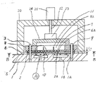
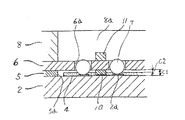
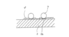
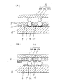
図1は、本発明を実施するためのはんだボール搭載装置の要部側面図、図2は図1のA部拡大図、図3はB−B矢視図である。1はベースである。2はワークで、表面には多数のパッド2aが形成されている。ワーク2は、ベース1に配置されたガイドピン3によりに水平方向に位置決めされ、ベース1に設けられた穴1a、1bに接続する図示を省略する吸引装置によりベース1上に固定されている。ワーク2の表面には予め所定の厚さにフラックス4が塗布されている。
【0013】
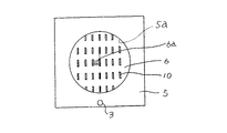
5は第1のライナマスクで、厚さはC1である。ライナマスク5の穴5aは、総てのマスク穴6aが内側に入る大きさに形成されている。6は整列マスクで、はんだボール7の直径より所定寸法だけ大きい(はんだボール7の直径の1.15倍程度)マスク穴6aがパッド2aと対向する位置に形成されている。整列マスク6の厚さははんだボールの直径程度である。8はマスク治具で、ライナマスク5および整列マスク6を保持している。9は直線案内装置で、ガイドピン3に係合するようにしてマスク治具8に固定されている。10は第2のライナマスクで、高さはC1以下であり、多数のライナマスク10がマスク穴6aと重ならないようにして整列マスク6の下面(ワーク2側の面。)に固定されている。11は抑え部材で、多数の抑え部材11がそれぞれ穴6aと重ならないようにしてマスク治具8に形成された中抜きの空間部8aの側面に固定されている。空間部8aは総てのマスク穴6aが内側に入る大きさに形成されている。
【0014】
20はコラムで、ベース1上に固定されている。21は上下送り装置で、コラム20に固定され、連結部22、加振装置23を介して取付部24を上下方向に移動させる。取付部24にはマスク治具8が固定されている。
【0015】
なお、図示を省略するはんだボール供給装置が、はんだボール7を空間部8aに供給する。また、整列マスク6の上面(空間部8aの面。)の余剰のはんだボールを除去する除去装置が設けられている。
【0016】
次に、はんだボールの整列手順を説明する。
(1)予め表面にフラックスを所定の厚さ(ただし、C1未満である。)塗布したワーク2を、ガイドピン3によりに水平方向に位置決めして、ベース1に載置する。そして、図示を省略した吸引装置を動作させ、ワーク2をベース1上に固定する。
(2)上下送り装置21を下降させ、ライナマスク5の下面をワーク2の表面に当接させる。このとき、フラックス4の表面と整列マスク6の下面との間には間隔C2が形成される。
(3)マスク穴6aの数以上のはんだボール7を整列マスク6上に供給し、総てのマスク穴6aにはんだボール7を入れる。
(4)図示しない除去装置により、余分なはんだボール7を除去する。
(5)上下送り装置21を上昇させる。このとき、加振装置23を動作させ、はんだボールマスクを穴6aに付着しないようにする。
(6)図4に示すように、はんだボール7が位置決めされたワーク2を図示しない加熱装置に移動させ、はんだボール7を溶融させてバンプを形成する。
【0017】
なお、マスク穴6aと同数のはんだボール7を整列マスク6に供給する場合、手順(4)は不要である。
【0018】
また、手順(3)において加振装置23を動作させると、はんだボール7をマスク穴6aに位置決めする時間を短縮することができる。
【0019】
また、ライナマスク10と抑え部材11とを設けたから、整列マスク6の面積を広くすることができるだけでなく厚さを薄くすることができる。したがって、例えば0.2mmのはんだボールを30,000個以上を同時に整列させることもできる。なお、図3ではライナマスク10を図の上下方向に分けるようにしたが、特に支障がない場合いには、上下方向のものを1個にまとめても良い。
【0020】
ところで、手順(5)において、はんだボール7をフラックス4に押し付けてフラックス4中に僅かに押し込むようにすると、はんだボール7がフラックス4の粘着力により保持され位置決めが確実になる。すなわち、図5(a)、(b)に示すように、マスク穴6aと同一の位置にはんだボール7の径より所定寸法だけ小さい径の球形の突起30aをプレート30bに設けた規制装置30を設け、整列マスク6とは独立に上下可能の装置に保持させておく。そして、図5(a)に示すように、手順(5)終了時点ではんだボール7を付勢するから、後工程の装置に移動させる際はんだボールの位置がずれない。さらに、整列マスク6を上昇させる際にも付勢を続けるから、はんだボール7が整列マスク6に付着することがない。
【0021】
なお、規制装置30は、上記と同様の方法で製作することができる。すなわち、プレート30bにパッド30cを形成してからバンプを形成し、突起物30aを乗せてから溶着すれよい。なお、突起30aは球形に限らず、半球、棒状あるいは針状のいずれであっても良い。
【0022】
なお、上記では、はんだボールの供給、整列、余分なはんだボールの除去等を自動で行うようにしたが、手動で行うようにしても良いことはいうまでもない。また、マスク治具6を上下移動だけでなく、ベース1とコラム20の間に水平移動のための案内機構とその駆動源を設け、上方で水平方向に移動させるようにしてもよい。
【0023】
【発明の効果】
以上説明したように、本発明によれば、作業工程が少なく、1度に2〜3万個のはんだボールを整列させることができるから、例えば8インチウエハ全域のような広い面積であっても、はんだボールを1回の作業で整列させることができる。したがって、作業が容易で、しかも作業能率を向上させることができる。また、ワークがウェハの場合、直径が標準化されているから、治具等の付属装置の種類を減らすことができるという効果もある。
【図面の簡単な説明】
【図1】本発明を実施するためのはんだボール搭載装置の要部側面図である。
【図2】図1のA部拡大図である。
【図3】図1のB−B矢視図である。
【図4】はんだボールをワークに位置決めした状態を示す正面断面図である。
【図5】はんだボールを確実にフラックス上に位置決めさせる方法の説明図である。
【符号の説明】
1 べース
2 ワーク
4 フラックス
6 整列マスク
6a マスク穴
7 はんだボール[0001]
BACKGROUND OF THE INVENTION
The present invention relates to a solder ball alignment method and a mask for positioning a solder ball at a pad position on a work surface such as a printed circuit board or a wafer.
[0002]
[Prior art]
In the ball grid array method (hereinafter referred to as BGA method), a solder ball is adsorbed to a mask in which a hole having a diameter smaller than that of the solder ball is formed in correspondence with the pad position on the workpiece surface, and the flux is absorbed in the solder ball. Flux was applied to the surface of the ball by immersing it slightly in the bath, and the solder ball was positioned on the pad via the applied flux.
[0003]
[Problems to be solved by the invention]
However, since the outer diameter of the solder balls varies, in the case of the BGA method, flux may adhere to the mask when flux is applied to the small-diameter solder balls. In some cases, it was not possible to leave the mask. For this reason, it is necessary to reduce the tolerance of the outer diameter of the ball and to always manage the height and flatness of the flux surface, and the work efficiency cannot be improved. Also, the number of solder balls that can be aligned at a time was up to about 1000.
[0004]
The object of the present invention is to solve the above-mentioned problems, to facilitate the work, and to arrange 30,000 to 30,000 solder balls at a time. It is an object of the present invention to provide a solder ball alignment method and a mask capable of aligning solder balls in the above operation.
[0005]
[Means for Solving the Problems]
In order to solve the above-mentioned problems, the invention of claim 1 is a solder ball alignment method in which a lower surface of a mask having a hole having a diameter larger than the diameter of the solder ball is applied to the surface of a work previously coated with a flux. After positioning slightly above the coating thickness of the flux, a solder ball is supplied to the hole, and then the solder ball positioned on the surface of the work is biased against the flux, and the solder ball is biased. However, the solder ball is positioned at the pad position on the workpiece surface by moving the mask away from the workpiece.
[0006]
According to a second aspect of the present invention, in the mask having a hole having a diameter larger than the diameter of the solder ball and having a plate thickness smaller than the diameter of the solder ball, the thickness is smaller than the thickness of the flux applied to the surface of the workpiece. One reinforcing member is disposed on the side facing the workpiece, and the second reinforcing member is disposed on the side not facing the workpiece .
[0012]
DETAILED DESCRIPTION OF THE INVENTION
Hereinafter, embodiments of the present invention will be described with reference to the drawings.
FIG. 1 is a side view of a main part of a solder ball mounting apparatus for carrying out the present invention, FIG. 2 is an enlarged view of a part A in FIG. 1, and FIG. 1 is a base.
[0013]
[0014]
A
[0015]
A solder ball supply device (not shown) supplies the
[0016]
Next, the procedure for aligning the solder balls will be described.
(1) A
(2) The
(3) The
(4)
(5) The
(6) As shown in FIG. 4, the
[0017]
When supplying the same number of
[0018]
Further, when the
[0019]
Further, since the
[0020]
By the way, in the procedure (5), when the
[0021]
In addition, the
[0022]
In the above description, supply and alignment of solder balls, removal of excess solder balls, and the like are performed automatically, but it goes without saying that they may be performed manually. Further, the
[0023]
【The invention's effect】
As described above, according to the present invention, the number of work steps is small, and 20,000 to 30,000 solder balls can be aligned at a time. The solder balls can be aligned in a single operation. Therefore, the work is easy and the work efficiency can be improved. Further, when the workpiece is a wafer, since the diameter is standardized, there is an effect that the types of attachment devices such as jigs can be reduced.
[Brief description of the drawings]
FIG. 1 is a side view of an essential part of a solder ball mounting apparatus for carrying out the present invention.
FIG. 2 is an enlarged view of a portion A in FIG.
FIG. 3 is a view taken along arrow BB in FIG. 1;
FIG. 4 is a front sectional view showing a state in which a solder ball is positioned on a workpiece.
FIG. 5 is an explanatory diagram of a method for reliably positioning a solder ball on a flux.
[Explanation of symbols]
1
Claims (2)
前記穴にはんだボールを供給し、
その後ワークの表面に位置決めした前記はんだボールを前記フラックスに対して付勢し、
前記はんだボールを付勢しながら前記マスクを前記ワークから遠ざけることによりはんだボールをワーク表面のパッド位置に位置決めすることを特徴とするはんだボールの整列方法。After positioning the lower surface of the mask having a hole having a diameter larger than the diameter of the solder ball slightly above the thickness of the flux applied from the surface of the work previously coated with the flux,
Supplying solder balls to the holes;
Thereafter, the solder balls positioned on the surface of the workpiece are urged against the flux,
A solder ball alignment method, wherein the solder ball is positioned at a pad position on a work surface by moving the mask away from the work while energizing the solder ball.
Priority Applications (1)
| Application Number | Priority Date | Filing Date | Title |
|---|---|---|---|
| JP14613698A JP4040749B2 (en) | 1998-05-27 | 1998-05-27 | Solder ball alignment method and mask |
Applications Claiming Priority (1)
| Application Number | Priority Date | Filing Date | Title |
|---|---|---|---|
| JP14613698A JP4040749B2 (en) | 1998-05-27 | 1998-05-27 | Solder ball alignment method and mask |
Publications (2)
| Publication Number | Publication Date |
|---|---|
| JPH11340364A JPH11340364A (en) | 1999-12-10 |
| JP4040749B2 true JP4040749B2 (en) | 2008-01-30 |
Family
ID=15400965
Family Applications (1)
| Application Number | Title | Priority Date | Filing Date |
|---|---|---|---|
| JP14613698A Expired - Fee Related JP4040749B2 (en) | 1998-05-27 | 1998-05-27 | Solder ball alignment method and mask |
Country Status (1)
| Country | Link |
|---|---|
| JP (1) | JP4040749B2 (en) |
Families Citing this family (2)
| Publication number | Priority date | Publication date | Assignee | Title |
|---|---|---|---|---|
| JP2002231752A (en) * | 2001-02-02 | 2002-08-16 | Tamura Seisakusho Co Ltd | Granular material mounting device |
| JP4849136B2 (en) * | 2009-01-29 | 2012-01-11 | 日本テキサス・インスツルメンツ株式会社 | Mounting method of conductive balls |
-
1998
- 1998-05-27 JP JP14613698A patent/JP4040749B2/en not_active Expired - Fee Related
Also Published As
| Publication number | Publication date |
|---|---|
| JPH11340364A (en) | 1999-12-10 |
Similar Documents
| Publication | Publication Date | Title |
|---|---|---|
| JP5008452B2 (en) | Solder ball mounting method and mounting device | |
| KR20190101293A (en) | Ball mounting device | |
| US6575351B1 (en) | Work/head positioning apparatus for ball mount apparatus | |
| JP4040749B2 (en) | Solder ball alignment method and mask | |
| WO2018061207A1 (en) | Machine for performing work on substrate, and insertion method | |
| JP4012647B2 (en) | Solder ball mounting method and apparatus | |
| JP4233190B2 (en) | Solder ball mounting method and apparatus | |
| KR100559729B1 (en) | Placement system apparatus and method | |
| JP3645795B2 (en) | Semiconductor device manufacturing method and semiconductor manufacturing apparatus | |
| JP2510688B2 (en) | Excess solder removal equipment | |
| JP2002171054A (en) | Solder ball mounting method and solder ball mounting device | |
| KR100283744B1 (en) | Method for Integrated Circuit Layout | |
| JP2001119133A (en) | Solder paste printing apparatus, solder paste printing method, wiring board, and method for manufacturing electric equipment | |
| US20230290666A1 (en) | Semiconductor manufacturing apparatus, carrier jig, and manufacturing method of semiconductor device | |
| JP2005056901A (en) | Semiconductor device manufacturing apparatus and semiconductor device manufacturing method | |
| JP3506273B2 (en) | Solder supply device and solder supply method | |
| JP2001015898A (en) | Mount head | |
| JP2009260096A (en) | Division processing method | |
| JP2008153457A (en) | Backup pin setting jig, substrate support device, surface mounter, cream solder printing device, substrate inspection device, and backup pin setting method | |
| JPH08309523A (en) | Mounting method of metal ball | |
| JP2001007136A (en) | Device and method for cleaning transfer head | |
| WO2026004886A1 (en) | Mounting apparatus | |
| JP4149718B2 (en) | Component mounting method | |
| JP2000260799A (en) | Apparatus and method for mounting conductive ball | |
| JP3733471B2 (en) | Work positioning and fixing device |
Legal Events
| Date | Code | Title | Description |
|---|---|---|---|
| A977 | Report on retrieval |
Free format text: JAPANESE INTERMEDIATE CODE: A971007 Effective date: 20050523 |
|
| A131 | Notification of reasons for refusal |
Free format text: JAPANESE INTERMEDIATE CODE: A131 Effective date: 20060411 |
|
| A521 | Request for written amendment filed |
Free format text: JAPANESE INTERMEDIATE CODE: A523 Effective date: 20060612 |
|
| A131 | Notification of reasons for refusal |
Free format text: JAPANESE INTERMEDIATE CODE: A131 Effective date: 20070828 |
|
| A521 | Request for written amendment filed |
Free format text: JAPANESE INTERMEDIATE CODE: A523 Effective date: 20071012 |
|
| TRDD | Decision of grant or rejection written | ||
| A01 | Written decision to grant a patent or to grant a registration (utility model) |
Free format text: JAPANESE INTERMEDIATE CODE: A01 Effective date: 20071106 |
|
| A61 | First payment of annual fees (during grant procedure) |
Free format text: JAPANESE INTERMEDIATE CODE: A61 Effective date: 20071108 |
|
| FPAY | Renewal fee payment (event date is renewal date of database) |
Free format text: PAYMENT UNTIL: 20101116 Year of fee payment: 3 |
|
| R150 | Certificate of patent or registration of utility model |
Free format text: JAPANESE INTERMEDIATE CODE: R150 |
|
| FPAY | Renewal fee payment (event date is renewal date of database) |
Free format text: PAYMENT UNTIL: 20111116 Year of fee payment: 4 |
|
| FPAY | Renewal fee payment (event date is renewal date of database) |
Free format text: PAYMENT UNTIL: 20111116 Year of fee payment: 4 |
|
| FPAY | Renewal fee payment (event date is renewal date of database) |
Free format text: PAYMENT UNTIL: 20121116 Year of fee payment: 5 |
|
| FPAY | Renewal fee payment (event date is renewal date of database) |
Free format text: PAYMENT UNTIL: 20131116 Year of fee payment: 6 |
|
| S533 | Written request for registration of change of name |
Free format text: JAPANESE INTERMEDIATE CODE: R313533 |
|
| R350 | Written notification of registration of transfer |
Free format text: JAPANESE INTERMEDIATE CODE: R350 |
|
| LAPS | Cancellation because of no payment of annual fees |