JP4040712B2 - Start pulse vertical signal generator and TFT liquid crystal display device gate drive method - Google Patents
Start pulse vertical signal generator and TFT liquid crystal display device gate drive method Download PDFInfo
- Publication number
- JP4040712B2 JP4040712B2 JP31462596A JP31462596A JP4040712B2 JP 4040712 B2 JP4040712 B2 JP 4040712B2 JP 31462596 A JP31462596 A JP 31462596A JP 31462596 A JP31462596 A JP 31462596A JP 4040712 B2 JP4040712 B2 JP 4040712B2
- Authority
- JP
- Japan
- Prior art keywords
- signal
- pulse
- vertical signal
- cpv
- pulse vertical
- Prior art date
- Legal status (The legal status is an assumption and is not a legal conclusion. Google has not performed a legal analysis and makes no representation as to the accuracy of the status listed.)
- Expired - Lifetime
Links
Images
Classifications
-
- G—PHYSICS
- G09—EDUCATION; CRYPTOGRAPHY; DISPLAY; ADVERTISING; SEALS
- G09G—ARRANGEMENTS OR CIRCUITS FOR CONTROL OF INDICATING DEVICES USING STATIC MEANS TO PRESENT VARIABLE INFORMATION
- G09G5/00—Control arrangements or circuits for visual indicators common to cathode-ray tube indicators and other visual indicators
-
- G—PHYSICS
- G09—EDUCATION; CRYPTOGRAPHY; DISPLAY; ADVERTISING; SEALS
- G09G—ARRANGEMENTS OR CIRCUITS FOR CONTROL OF INDICATING DEVICES USING STATIC MEANS TO PRESENT VARIABLE INFORMATION
- G09G3/00—Control arrangements or circuits, of interest only in connection with visual indicators other than cathode-ray tubes
- G09G3/20—Control arrangements or circuits, of interest only in connection with visual indicators other than cathode-ray tubes for presentation of an assembly of a number of characters, e.g. a page, by composing the assembly by combination of individual elements arranged in a matrix no fixed position being assigned to or needed to be assigned to the individual characters or partial characters
- G09G3/34—Control arrangements or circuits, of interest only in connection with visual indicators other than cathode-ray tubes for presentation of an assembly of a number of characters, e.g. a page, by composing the assembly by combination of individual elements arranged in a matrix no fixed position being assigned to or needed to be assigned to the individual characters or partial characters by control of light from an independent source
- G09G3/36—Control arrangements or circuits, of interest only in connection with visual indicators other than cathode-ray tubes for presentation of an assembly of a number of characters, e.g. a page, by composing the assembly by combination of individual elements arranged in a matrix no fixed position being assigned to or needed to be assigned to the individual characters or partial characters by control of light from an independent source using liquid crystals
- G09G3/3611—Control of matrices with row and column drivers
- G09G3/3648—Control of matrices with row and column drivers using an active matrix
-
- G—PHYSICS
- G09—EDUCATION; CRYPTOGRAPHY; DISPLAY; ADVERTISING; SEALS
- G09G—ARRANGEMENTS OR CIRCUITS FOR CONTROL OF INDICATING DEVICES USING STATIC MEANS TO PRESENT VARIABLE INFORMATION
- G09G2310/00—Command of the display device
- G09G2310/02—Addressing, scanning or driving the display screen or processing steps related thereto
- G09G2310/0243—Details of the generation of driving signals
- G09G2310/0251—Precharge or discharge of pixel before applying new pixel voltage
-
- G—PHYSICS
- G09—EDUCATION; CRYPTOGRAPHY; DISPLAY; ADVERTISING; SEALS
- G09G—ARRANGEMENTS OR CIRCUITS FOR CONTROL OF INDICATING DEVICES USING STATIC MEANS TO PRESENT VARIABLE INFORMATION
- G09G3/00—Control arrangements or circuits, of interest only in connection with visual indicators other than cathode-ray tubes
- G09G3/20—Control arrangements or circuits, of interest only in connection with visual indicators other than cathode-ray tubes for presentation of an assembly of a number of characters, e.g. a page, by composing the assembly by combination of individual elements arranged in a matrix no fixed position being assigned to or needed to be assigned to the individual characters or partial characters
- G09G3/34—Control arrangements or circuits, of interest only in connection with visual indicators other than cathode-ray tubes for presentation of an assembly of a number of characters, e.g. a page, by composing the assembly by combination of individual elements arranged in a matrix no fixed position being assigned to or needed to be assigned to the individual characters or partial characters by control of light from an independent source
- G09G3/36—Control arrangements or circuits, of interest only in connection with visual indicators other than cathode-ray tubes for presentation of an assembly of a number of characters, e.g. a page, by composing the assembly by combination of individual elements arranged in a matrix no fixed position being assigned to or needed to be assigned to the individual characters or partial characters by control of light from an independent source using liquid crystals
- G09G3/3611—Control of matrices with row and column drivers
- G09G3/3674—Details of drivers for scan electrodes
- G09G3/3677—Details of drivers for scan electrodes suitable for active matrices only
Landscapes
- Engineering & Computer Science (AREA)
- Physics & Mathematics (AREA)
- Computer Hardware Design (AREA)
- General Physics & Mathematics (AREA)
- Theoretical Computer Science (AREA)
- Chemical & Material Sciences (AREA)
- Crystallography & Structural Chemistry (AREA)
- Liquid Crystal Display Device Control (AREA)
- Control Of Indicators Other Than Cathode Ray Tubes (AREA)
- Transforming Electric Information Into Light Information (AREA)
- Synchronizing For Television (AREA)
Description
【0001】
【発明の属する技術分野】
本発明はデータイネーブル信号(Data Enable Signal;DE) を用いてBIOS(Basic Input Output System) と無関係にプレチャージするスタートパルス垂直(Start Pulse Vertical;STV) 信号生成器に係り、より詳しくは、液晶表示装置の駆動回路において、ゲートを駆動するためのSTV信号を入力するとき、BIOSと無関係に二つ前のクロックにおいてプレチャージ用STV信号を生成せしめることにより、実際データが入るメインSTV信号以前に一次的にパネルのゲートをオンさせてデータを入力し、メインSTV信号が入力されるときゲートの駆動速度を速くするデータイネーブル信号DEを用いてBIOSと無関係にプレチャージするSTV信号生成器に関する。
【0002】
【従来の技術】
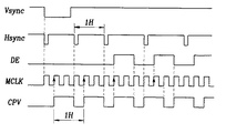
一般的なPCセットにおいては、ディスプレーのための制御信号として垂直同期信号Vsync 、水平同期信号Hsync 、データイネーブル信号DE、メインクロック信号MCLKおよびデータ(色信号)を生成している。このようなPCセットにおいて、同期モード(Sync Mode) とはデータ制御のため垂直同期信号Vsync 、水平同期信号Hsync に各種信号を生成することをいい、DEモードとはデータ制御のためデータイネーブル信号DEにデータ制御信号を生成することをいう。
【0003】
PCセットメーカーによっては、垂直同期信号Vsync 、水平同期信号Hsync およびデータイネーブル信号DEを全て提供する場合と、垂直同期信号Vsync 、水平同期信号Hsync のみを提供する場合並びに、データイネーブル信号DEのみを提供する場合がある。メインクロック信号MCLKとデータは同期モードやDEモードに関係なしで常に提供される。
【0004】
垂直同期信号Vsync はディスプレー装置の垂直ラインを制御するための信号であり、水平同期信号Hsync は水平ラインを動作するための信号である。
同期信号は一般的なモニターを用いるとき制御のために生成する信号であり、データイネーブル信号は液晶表示装置用フラットパネルを制御するために適当であるように生成する信号である。
【0005】
モニターは電子銃により1次元に画面構成を動作させ、液晶表示装置パネルはロー、カラムにより2次元に画面を構成する。
BIOSは同期モード、DEモードいずれの場合にも適応でき、制御信号の各種情報などの変化を可能にする。
これを図3および図4に示す。
【0006】
BIOSはシステムの効用性を高めるため出力を行うタイミングを可変可能にし、例えば図4の同期モードにおいてデータ‘1’は水平同期信号後にメインクロック信号MCLKを三つ経てから出力される。
この場合、設計時にメインクロック信号三つの後、データ‘1’を処理するように設定しているが、他のPCセットメーカーにおいて水平同期信号後に四つのメインクロック信号を経た後データが出力されるように設定されている場合、BIOSを変更しなければならない。
【0007】
クロックパルス垂直信号(Clock Pulse Vertical Signal; CPV) はVGA方式で用いられ、このVGA方式では、画素として640カラム*480ロー*RGB個の有効データ個数が存在する。
しかしながら、実際タイミングを見るとき、制御信号はブランク期間を有しており、有効データ個数より多い800*525のメインクロック個数からなる。
【0008】
ブランク期間では、電子銃が画面にデータを走査するとき水平方向に帰線する時間と垂直方向に帰線する時間が必要であり、この時間の間はデータを入力しても画面には表れない。
1水平同期信号は800個のメインクロックが集まって構成され、1垂直同期信号は水平同期信号525個が集まって構成される。
【0009】
1水平同期信号に係る信号はメインクロック信号からつくって用いるが、1垂直同期信号に係る信号をメインクロック信号からつくる場合、800*525個のメインクロック信号をカウントしなければならないので非効率的であり、通常、垂直同期信号に係る垂直ライン制御信号などは1水平同期信号と周期が同一であるCPV信号を生成して用いる。
【0010】
このCPV信号はゲートドライバー集積回路を動作するための基準信号になり、ゲート信号と関連するすべての信号を生成することになる。
一般的に、液晶表示装置の内部ではデータイネーブル信号DEとメインクロック信号を生成しており、この信号を用いて実際必要な信号を生成して用いている。
【0011】
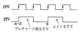
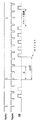
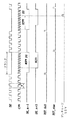
この場合、液晶表示装置のゲートドライブを駆動するためのクロックパルスとしてCPV信号を用い、ゲートドライブの動作時点を知らせるためSTV信号を用いるが、これを図1に示す。
図1に示すように、STV信号をみるとメインSTV信号よりCPV信号2つ前のクロックn−2において任意のSTVを生成してプレチャージさせる。
【0012】
そうすると、実際データが入力されるメインSTV信号以前に1次的にパネルのゲートをスイッチオンさせ、データを入力してメインSTV信号が動作する速度を高めることになり、結果的にゲートが正確な時点で動作を始めることになる。
従来では前記のようなSTV信号を生成するために垂直同期信号Vsync を用いており、これを図2に示す。このように、従来では垂直同期信号を基準にして一定時間T後にPre−STV信号を発生させていた。
【0013】
【発明が解決しようとする課題】
しかしながら、前記過程において垂直同期信号を基準にしてPre−STV信号を発生する際の遅延時間Tは企業ごとに一定していない。すなわち、垂直同期信号を基準にして任意の一定時間Tだけ遅延するPre−STV信号をつくる場合、各企業の製品のBIOSによりPre−STV信号が生成されるタイミングが異なるため、毎回BIOSをセットアップさせなければならないという問題がある。
【0014】
つまり、従来のSTV信号生成器では各企業ごとにBIOSが異なるため、毎回BIOSをセットアップさせなければならないという短所がある。
従来のPre−STV信号生成法とBIOSに従う補正方法について説明する。
図5または図9に示すように、プレチャージ用STV信号はポイントAにおいて有効データが出力されるため、基準信号になる‘n+2’期間より以前であるn番目の位置において発生し得るように垂直同期信号Vsync のローパルス信号からカウントしてつくらせる。
【0015】
このため、設計したシステムのプレチャージSTV信号のnが100であって、B社の場合nが150個必要であるとすると、BIOSでブランク期間の基準信号を変更し、システムに適合するように150個を100個に変更しなければならない。
本発明はこのようなBIOSの修正をすることなく、プレチャージSTV信号の位置が図5のポイントAに示す有効データが出力する位置において常に一定となるようにし、例えば、nの個数が100個または150個と無関係に常に一定の位置に発生するようにして、画面においてデータ損失をなくし、BIOS調整の煩わしさを少なくしようとするものである。
【0016】
さらに、図5に示すように、n+2後であるポイントAにおいて有効データが出力されるように回路設計した時のnの個数を100に固定すると、垂直同期信号Vsync の後CPV信号102(n+2)個後にSTV信号が発生することになるが、回路設計されたシステムはハードウェア的に構成されるため、最初の設計時に102個後にSTV信号を生成するようにすると、この値は再び回路設計するまでは変化することなく固定してしまう。図6にCPV信号が生成される過程の波形を示す。
【0017】
この方法はBIOSの値を変動することで、nの個数をPCセットにおいて常に対応させて設計システムと同一にする方法を用いているが、煩わしいという短所がある。
従って、本発明は前記のような短所を解決するためのものであって、その目的は、BIOSと無関係に動作するデータイネーブル信号DEを用いてPre−STV信号を生成することにより、BIOSセットアップが必要でない、BIOSと無関係にプレチャージするスタートパルス垂直信号生成器を提供することにある。
【0018】
【課題を解決するための手段】
本発明に係るスタートパルス垂直信号生成器は、データイネーブル信号DEとメインクロック信号が入力され、これをカウントしてクロックパルス垂直信号CPVを生成するクロックパルス垂直信号生成部と、前記クロックパルス垂直信号CPVとデータイネーブル信号DEとが入力され、各種パルス信号を生成するパルス信号生成部と、前記クロックパルス垂直信号生成部のクロックパルス垂直信号CPVとパルス信号生成部から出力される各種パルス信号が入力され、スタートパルス垂直信号STVを生成するスタートパルス垂直信号生成部とを含んで構成される。
【0019】
さらに、本発明のTFT液晶表示装置のゲート駆動方法では、最初に入力されるブランク期間をクロックパルス垂直信号CPVの周期でカウントした値と、前記ブランク期間を最小限1周期以上遅延させてCPVでカウントした値を所定の周期で貯蔵し、次のDEのブランク信号のブランク期間の始まりから前記1周期以上遅延させたCPVの周期後にプレチャージSTV信号を出力するようにすることを特徴とする。
【0020】
【発明の実施の形態】
以下、本発明の好ましい実施形態を添付図面に基づいて詳細に説明する。
図7は本発明の1実施形態に従うスタートパルス垂直信号生成器(以下、STV信号生成器と称す)のブロック構成図であり、図8は本発明の実施形態に従うSTV信号生成器内のスタートパルス垂直信号生成部(以下、STV信号生成部と称す)の詳細図である。
【0021】
図7に示すように、本発明の実施形態に従うSTV信号生成器の構成は、データイネーブル信号DEとメインクロック信号MCLKが入力され、これをカウントしてクロックパルス垂直信号CPVを生成するためのクロックパルス垂直信号生成部1と、前記クロックパルス垂直信号生成部1に連結され、前記クロックパルス垂直信号CPVとデータイネーブル信号DEが入力され、各種パルス信号(DE_n+1,DE_n+3,RST_rise,RST_fall)を生成するためのパルス信号生成部2と、前記クロックパルス垂直信号生成部1のクロックパルス垂直信号CPVとパルス信号生成部2から出力される各種パルス信号(DE_n+1,DE_n+3,RST_rise,RST_fall)が入力され、プレチャージスタートパルス垂直信号Pre−STVを生成するためのプレチャージSTV信号生成部3とからなる。
【0022】
図8に示すように、前記プレチャージSTV信号生成部3の構成は、データイネーブル信号DEをクロックパルス垂直信号CPVの1クロック信号分遅延した信号(DE_n+1)とリセット信号(RST_rise)が入力され、ブランク期間の間カウントするためのDE_n+1カウンタ31と、データイネーブル信号DEをクロックパルス垂直信号CPVの3クロック信号分遅延した信号(DE_n+3)とリセット信号(RST_fall)が入力され、ブランク期間よりクロックパルス垂直信号CPVの2クロック信号分遅れてブランク期間の間カウントするためのDE_n+3カウンタ34と、前記DE_n+3カウンタ34のカウント値を貯蔵するためのカウンタ値貯蔵器33と、前記カウンタ値貯蔵器33のカウント値と前記DE_n+1カウンタ31の値を比較して同一である場合、パルス信号を発生するためのカウンタ比較器32と、前記カウンタ比較器32から出力されるパルス信号が入力されてプレチャージスタートパルス垂直信号を出力するためのSTV信号生成器35とからなる。
【0023】
まず、この発明の基本概念について簡単に説明する。
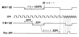
図10に示すように、データイネーブル信号DEよりクロックパルス垂直信号CPV2つ分前にBIOSと無関係にプレチャージ用クロックパルス垂直信号STVを生成することである。
DEをもってCPVを生成する場合、DEの立上り部分においてカウントし始めて所望する時間後にCPVの立上りエッジまたは立下りエッジを形成し、次のDE立上りエッジが入る前にCPVのまた他のエッジ部分を形成する。これを図11に示す。
【0024】
DEが存在する区間のCPV信号周期T1はDE信号周期または垂直同期信号Hsync 周期と同様であり、ブランク期間のCPV信号周期はT1と同様にすることができるが、BIOS可変にもっと効果的にT1と同様に合わせることよりCPVを生成するカウンタ1周期(10ビットカウンタは1024個のメインクロック信号)T2につくることがずっと合理的であり、本発明の回路においてもこのように適用した。
【0025】
すなわち、最初のデータイネーブル信号DEとクロックパルス垂直信号CPVが入力されるとき、ブランク期間のクロックパルス垂直信号CPV値が可変しても常にデータイネーブル信号DEのスタートより二つのクロックパルス垂直信号CPV前でプレチャージさせる信号を生成することである。
まず、最初のデータイネーブル信号DEのブランク期間の長さよりクロックパルス垂直信号CPV2つ分短いブランク期間の任意のデータイネーブル信号DEを生成する。
【0026】
任意のデータイネーブル信号DEのブランク期間内のクロックパルス垂直信号CPVの個数を数えて(3CPV)この値を貯蔵し、この後、最初のデータイネーブル信号DEの次のブランク期間が始まる部分からカウントを開始して、任意のデータイネーブル信号DEのブランク期間のカウンタ値と同一のカウント値で、パルスを発生させると、最初のデータイネーブル信号DEのブランク期間において所望のタイミングで任意のパルスを発生するようにすることができる。ここでは、クロックパルス垂直信号CPVの2クロック信号分前のタイミングでパルスを発生させることができる。
【0027】
さらに、クロックパルス垂直信号CPVの個数が変わっても常に最初のデータイネーブル信号DEのデータイネーブルスタートポイントにおいてクロックパルス垂直信号CPV2つ分だけ先行して信号を生成できる。
前記構成によるこの発明の実施形態に従うSTV信号生成器の作用について説明する。
【0028】
まず、使用者により電源が印加されると、この発明の実施形態に従うBIOSと無関係にプレチャージするSTV信号生成器の動作が始まる。
動作が始まると、図9に示すような波形を有するデータイネーブル信号DEおよびメインクロック信号MCLKがクロックパルス垂直信号生成部(CPV信号生成部)1に入力される。
【0029】
そうすると、クロックパルス垂直信号生成部1においてはクロックパルス垂直信号CPVを生成して出力する。
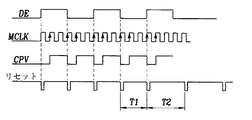
各種のパルス信号生成部2においては前記クロックパルス垂直信号生成部1から出力されるクロックパルス垂直信号CPVとメインクロック信号MCLKが入力されて各種信号(DE_n+1,DE_n+3,RST_rise,RST_fall)を生成する。この信号を図9に示す。
【0030】
次に、DE_n+1カウンタ31はデータイネーブル信号DEをクロックパルス垂直信号CPVの1クロック信号分遅延した信号DE_n+1とリセット信号RST_riseが入力され、クロックパルス垂直信号CPVのブランク期間の間カウントする。
同時に、DE_n+3カウンタ34はデータイネーブル信号DEをクロックパルス垂直信号CPVの3クロック信号分遅延した信号DE_n+3とリセット信号RST_fallが入力され、クロックパルス垂直信号CPV2つ分遅延して、ブランク期間の間カウントする。
【0031】
カウンタ値貯蔵器33は前記DE_n+3カウンタ34のカウント値を貯蔵する。
次に、図9に示すように、カウンタ比較器32は次のブランク期間が始まると、前記カウンタ値貯蔵器33のカウント値と前記DE_n+1カウンタ31値を比較し、同一になったとき、パルス信号を発生させる。
【0032】
その後、Pre−STV信号生成器35は前記カウンタ比較器32から出力されるパルス信号が入力されプレチャージスタートパルス垂直信号を出力する。
【0033】
【発明の効果】
以上のように、本発明の実施例において、ゲートを駆動するためのSTV信号を入力するとき、BIOSと無関係に2つ前のクロックにおいてプレチャージ用STV信号を生成せしめることにより、実際にデータが入るメインSTV信号以前に1次的にパネルのゲートをオンさせ、データを入力してメインSTV信号が入力されるとき、ゲートの駆動速度を速くするデータイネーブル信号DEを用いてBIOSと無関係にプレチャージするSTV信号生成器を提供することができる。
【図面の簡単な説明】
【図1】一般的なSTVを示す波形図である。
【図2】従来の一般的な垂直同期信号を用いたSTV信号生成過程を示す波形図である。
【図3】BIOSに係わる各信号の波形図である。
【図4】BIOSに係わる各信号の波形図である。
【図5】従来のプレチャージSTV信号生成法とBIOSに従う補正方法を示す波形図である。
【図6】CPV信号生成法に従う各信号の波形図である。
【図7】本発明の実施例に従うBIOSと無関係にプレチャージするSTV信号生成器のブロック構成図である。
【図8】本発明の実施例に従うBIOSと無関係にプレチャージするSTV信号生成器内のSTV信号生成部の詳細図である。
【図9】本発明の実施例に従うBIOSと無関係にプレチャージするSTV信号生成器に用いられるそれぞれの信号波形図である。
【図10】本発明の実施例に従うBIOSと無関係にプレチャージするSTV信号生成器の動作を示す簡単な概念図である。
【図11】データイネーブル信号DEをもってCPVを生成する過程の各信号の波形図である。
【符号の説明】
1 クロックパルス垂直信号生成部
2 パルス信号生成部
3 プレチャージSTV信号生成部
31 DE_n+1カウンタ
32 カウンタ比較器
33 カウンタ値貯蔵器
34 DE_n+3カウンタ
35 Pre−STV信号生成器[0001]
BACKGROUND OF THE INVENTION
The present invention relates to a start pulse vertical (STV) signal generator that precharges independently of a BIOS (Basic Input Output System) using a data enable signal (DE). When the STV signal for driving the gate is input in the driving circuit of the display device, the precharge STV signal is generated in the previous two clocks regardless of the BIOS, so that the main data before the main STV signal into which the actual data is input is generated. The present invention relates to an STV signal generator that pre-charges data independently of BIOS by using a data enable signal DE that temporarily turns on a panel gate to input data and inputs a main STV signal to increase the gate drive speed.
[0002]
[Prior art]
In a general PC set, a vertical synchronization signal Vsync, a horizontal synchronization signal Hsync, a data enable signal DE, a main clock signal MCLK, and data (color signal) are generated as control signals for display. In such a PC set, the synchronization mode (Sync Mode) means that various signals are generated for the vertical synchronization signal Vsync and the horizontal synchronization signal Hsync for data control, and the DE mode is the data enable signal DE for data control. The generation of a data control signal.
[0003]
Depending on the PC set maker, the vertical sync signal Vsync, the horizontal sync signal Hsync, and the data enable signal DE are all provided, the vertical sync signal Vsync, the horizontal sync signal Hsync only, and the data enable signal DE only are provided. There is a case. The main clock signal MCLK and data are always provided regardless of the synchronous mode or the DE mode.
[0004]
The vertical synchronization signal Vsync is a signal for controlling the vertical line of the display device, and the horizontal synchronization signal Hsync is a signal for operating the horizontal line.
The synchronization signal is a signal generated for control when a general monitor is used, and the data enable signal is a signal generated as appropriate for controlling the flat panel for a liquid crystal display device.
[0005]
The monitor operates the screen configuration in one dimension with an electron gun, and the liquid crystal display panel configures the screen in two dimensions with rows and columns.
The BIOS can be applied to both the synchronous mode and the DE mode, and can change various information of the control signal.
This is shown in FIG. 3 and FIG.
[0006]
The BIOS makes it possible to vary the output timing in order to enhance the utility of the system. For example, in the synchronous mode of FIG. 4, the data “1” is output after three main clock signals MCLK after the horizontal synchronous signal.
In this case, the data '1' is set to be processed after the three main clock signals at the time of design, but the data is output after passing the four main clock signals after the horizontal sync signal in other PC set manufacturers. If so, the BIOS must be changed.
[0007]
A clock pulse vertical signal (CPV) is used in the VGA method, and in this VGA method, there are 640 columns * 480 rows * RGB effective data numbers as pixels.
However, when looking at the actual timing, the control signal has a blank period and consists of the number of main clocks of 800 * 525 which is larger than the number of valid data.
[0008]
In the blank period, when the electron gun scans data on the screen, it takes time to return in the horizontal direction and time to return in the vertical direction. During this time, even if data is input, it does not appear on the screen. .
One horizontal synchronization signal is composed of 800 main clocks, and one vertical synchronization signal is composed of 525 horizontal synchronization signals.
[0009]
A signal related to one horizontal sync signal is generated from a main clock signal and used. However, when a signal related to one vertical sync signal is generated from a main clock signal, it is inefficient because 800 * 525 main clock signals must be counted. In general, a vertical line control signal or the like related to a vertical synchronization signal is generated by using a CPV signal having the same period as one horizontal synchronization signal.
[0010]
The CPV signal becomes a reference signal for operating the gate driver integrated circuit, and generates all signals related to the gate signal.
In general, a data enable signal DE and a main clock signal are generated inside the liquid crystal display device, and signals that are actually required are generated and used.
[0011]
In this case, the CPV signal is used as a clock pulse for driving the gate drive of the liquid crystal display device, and the STV signal is used to notify the operation time of the gate drive, which is shown in FIG.
As shown in FIG. 1, when the STV signal is viewed, an arbitrary STV is generated and precharged at a clock n-2 two CPV signals before the main STV signal.
[0012]
Then, the gate of the panel is first switched on before the main STV signal to which actual data is input, and the speed at which the main STV signal operates by inputting data is increased. As a result, the gate is accurate. It will start working at that point.
Conventionally, the vertical synchronization signal Vsync is used to generate the STV signal as described above, and this is shown in FIG. Thus, conventionally, the Pre-STV signal is generated after a predetermined time T with reference to the vertical synchronization signal.
[0013]
[Problems to be solved by the invention]
However, the delay time T when generating the Pre-STV signal based on the vertical synchronization signal in the above process is not constant for each company. That is, when creating a Pre-STV signal that is delayed by an arbitrary fixed time T with respect to the vertical synchronization signal, the timing of generating the Pre-STV signal differs depending on the BIOS of each company's product. There is a problem of having to.
[0014]
In other words, the conventional STV signal generator has a disadvantage that the BIOS is different for each company, so that the BIOS must be set up every time.
A conventional Pre-STV signal generation method and a correction method according to the BIOS will be described.
As shown in FIG. 5 or FIG. 9, since the valid data is output at the point A, the precharge STV signal is vertical so that it can be generated at the nth position before the 'n + 2' period that becomes the reference signal. Count from the low pulse signal of the sync signal Vsync.
[0015]
For this reason, if n of the precharge STV signal of the designed system is 100 and 150 is necessary in the case of company B, the blank period reference signal is changed by BIOS so that it matches the system. 150 pieces must be changed to 100 pieces.
In the present invention, without correcting the BIOS, the position of the precharge STV signal is always constant at the position where the valid data indicated by the point A in FIG. 5 is output. For example, the number of n is 100. Alternatively, it is always generated at a fixed position regardless of 150, thereby eliminating data loss on the screen and reducing the troublesomeness of BIOS adjustment.
[0016]
Further, as shown in FIG. 5, when the number of n when the circuit is designed so that valid data is output at point A after n + 2 is fixed to 100, the CPV signal 102 (n + 2) after the vertical synchronization signal Vsync is fixed. The STV signal is generated after the number of units. However, since the circuit designed system is configured by hardware, if the STV signal is generated after 102 units at the initial design, this value is designed again. Until it is fixed without change. FIG. 6 shows a waveform in the process of generating the CPV signal.
[0017]
This method uses a method in which the number of n is always made to correspond in the PC set by changing the BIOS value so as to be the same as that of the design system, but there is a disadvantage that it is troublesome.
Accordingly, the present invention is to solve the above disadvantages, and the purpose of the present invention is to generate a Pre-STV signal using a data enable signal DE that operates independently of the BIOS, thereby enabling the BIOS setup. It is an object of the present invention to provide a start pulse vertical signal generator which is not necessary and precharges independently of the BIOS.
[0018]
[Means for Solving the Problems]
The start pulse vertical signal generator according to the present invention receives a data enable signal DE and a main clock signal, counts them to generate a clock pulse vertical signal CPV, and the clock pulse vertical signal A CPV and a data enable signal DE are input, a pulse signal generation unit that generates various pulse signals, a clock pulse vertical signal CPV of the clock pulse vertical signal generation unit, and various pulse signals output from the pulse signal generation unit are input. And a start pulse vertical signal generator for generating a start pulse vertical signal STV.
[0019]
Further, according to the gate driving method of the TFT liquid crystal display device of the present invention, the blank period input first is counted by the period of the clock pulse vertical signal CPV, and the blank period is delayed by at least one period to obtain the CPV. The counted value is stored in a predetermined cycle, and the precharge STV signal is output after the CPV cycle delayed by at least one cycle from the start of the blank period of the next DE blank signal.
[0020]
DETAILED DESCRIPTION OF THE INVENTION
Hereinafter, preferred embodiments of the present invention will be described in detail with reference to the accompanying drawings.
FIG. 7 is a block diagram of a start pulse vertical signal generator (hereinafter referred to as an STV signal generator) according to an embodiment of the present invention, and FIG. 8 is a start pulse in the STV signal generator according to an embodiment of the present invention. It is a detailed view of a vertical signal generation unit (hereinafter referred to as an STV signal generation unit).
[0021]
As shown in FIG. 7, the configuration of the STV signal generator according to the embodiment of the present invention is configured to receive a data enable signal DE and a main clock signal MCLK, and count them to generate a clock pulse vertical signal CPV. The pulse vertical
[0022]
As shown in FIG. 8, the precharge
[0023]
First, the basic concept of the present invention will be briefly described.
As shown in FIG. 10, the precharge clock pulse vertical signal STV is generated irrespective of the BIOS two clock pulse vertical signals CPV before the data enable signal DE.
When generating CPV with DE, start counting at the rising portion of DE and form the rising or falling edge of CPV after the desired time and form the other edge portion of CPV before the next DE rising edge To do. This is shown in FIG.
[0024]
The CPV signal period T1 in the section where DE exists is the same as the DE signal period or the vertical synchronization signal Hsync period, and the CPV signal period in the blank period can be the same as T1, but it is more effective for BIOS variable. It is much more reasonable to make it in one cycle of the counter (10-bit counter is 1024 main clock signals) T2 to generate CPV by matching in the same manner as described above, and this is also applied to the circuit of the present invention.
[0025]
That is, when the first data enable signal DE and the clock pulse vertical signal CPV are input, even if the clock pulse vertical signal CPV value in the blank period is variable, the clock enable signal DE is always two clock pulse vertical signals CPV before the start of the data enable signal DE. Is to generate a signal to be precharged.
First, an arbitrary data enable signal DE having a blank period shorter by two clock pulse vertical signals CPV than the length of the blank period of the first data enable signal DE is generated.
[0026]
Count the number of clock pulse vertical signals CPV in the blank period of any data enable signal DE (3 CPV), store this value, and then count from the beginning of the next blank period of the first data enable signal DE When a pulse is generated with the same count value as the counter value of the blank period of the arbitrary data enable signal DE, the arbitrary pulse is generated at a desired timing in the blank period of the first data enable signal DE. Can be. Here, a pulse can be generated at a timing two clock signals before the clock pulse vertical signal CPV.
[0027]
Furthermore, even if the number of clock pulse vertical signals CPV changes, a signal can always be generated ahead of two clock pulse vertical signals CPV at the data enable start point of the first data enable signal DE.
The operation of the STV signal generator according to the embodiment of the present invention having the above configuration will be described.
[0028]
First, when the power is applied by the user, the operation of the STV signal generator for precharging is started regardless of the BIOS according to the embodiment of the present invention.
When the operation starts, a data enable signal DE and a main clock signal MCLK having waveforms as shown in FIG. 9 are input to the clock pulse vertical signal generation unit (CPV signal generation unit) 1.
[0029]
Then, the clock pulse vertical
The various
[0030]
Next, the DE_n + 1
At the same time, the DE_n + 3
[0031]
The
Next, as shown in FIG. 9, when the next blank period starts, the
[0032]
Thereafter, the
[0033]
【The invention's effect】
As described above, in the embodiment of the present invention, when the STV signal for driving the gate is input, the precharge STV signal is generated in the previous two clocks regardless of the BIOS, so that the data is actually transmitted. When the main STV signal is input by first turning on the gate of the panel before the main STV signal is input, the data enable signal DE for increasing the gate drive speed is used for pre-regarding the BIOS. An STV signal generator for charging can be provided.
[Brief description of the drawings]
FIG. 1 is a waveform diagram showing a general STV.
FIG. 2 is a waveform diagram illustrating an STV signal generation process using a conventional general vertical synchronization signal.
FIG. 3 is a waveform diagram of signals related to BIOS.
FIG. 4 is a waveform diagram of signals related to the BIOS.
FIG. 5 is a waveform diagram showing a conventional precharge STV signal generation method and a correction method according to BIOS.
FIG. 6 is a waveform diagram of each signal according to the CPV signal generation method.
FIG. 7 is a block diagram of an STV signal generator that precharges independently of a BIOS according to an embodiment of the present invention.
FIG. 8 is a detailed view of an STV signal generator in an STV signal generator that precharges regardless of the BIOS according to an embodiment of the present invention;
FIG. 9 is a signal waveform diagram used for an STV signal generator that precharges independently of the BIOS according to an embodiment of the present invention.
FIG. 10 is a simple conceptual diagram illustrating the operation of an STV signal generator that precharges independently of a BIOS according to an embodiment of the present invention.
FIG. 11 is a waveform diagram of each signal in the process of generating a CPV with a data enable signal DE.
[Explanation of symbols]
DESCRIPTION OF
Claims (5)
前記クロックパルス垂直信号CPVのパルスをカウントし、そのカウントに基づいて前記データイネーブル信号DEを遅延させて遅延パルス信号を生成し、かつ、前記データイネーブル信号DEの状態に応じてブランク期間の開始時点と終了時点とでリセットパルス信号を生成するパルス信号生成部と、
前記リセットパルス信号に応じてリセットされ、前記遅延パルス信号に応じてブランク期間で前記クロックパルス垂直信号CPVのパルスをカウントし、そのカウントに基づき、ブランク期間の終了時点より前記クロックパルス垂直信号CPVの周期の所定数倍分先行してプレチャージスタートパルス垂直信号を生成するプレチャージスタートパルス垂直信号生成部と、
を有するスタートパルス垂直信号生成器。 A clock pulse for inputting a data enable signal DE and a main clock signal from the outside , counting pulses of the main clock signal every time the data enable signal DE changes, and generating a clock pulse vertical signal CPV based on the count A vertical signal generator;
The pulse of the clock pulse vertical signal CPV is counted, the data enable signal DE is delayed based on the count to generate a delayed pulse signal, and the start time of the blank period according to the state of the data enable signal DE And a pulse signal generator that generates a reset pulse signal at the end time ,
The clock pulse vertical signal CPV is reset in response to the reset pulse signal, and the clock pulse vertical signal CPV is counted in a blank period in response to the delay pulse signal. Based on the count, the clock pulse vertical signal CPV is counted from the end of the blank period. A precharge start pulse vertical signal generation unit for generating a precharge start pulse vertical signal by a predetermined number of times in advance of the cycle ;
A start pulse vertical signal generator.
前記データイネーブル信号DEを前記クロックパルス垂直信号CPVの1周期分遅延させた第1遅延パルス信号DE_n+1と、
前記データイネーブル信号DEを前記クロックパルス垂直信号CPVの3周期分遅延させた第2遅延パルス信号DE_n+3と、
を含み、
前記リセットパルス信号は、
前記第1遅延パルス信号DE_n+1に応じて前記プレチャージスタートパルス垂直信号生成部によって行われる前記クロックパルス垂直信号CPVのパルスのカウントをリセットするための第1リセット信号RST_riseと、
前記第2遅延パルス信号DE_n+3に応じて前記プレチャージスタートパルス垂直信号生成部によって行われる前記クロックパルス垂直信号CPVのパルスのカウントをリセットするための第2リセット信号RST_fallと、
を含む、請求項1に記載のスタートパルス垂直信号生成器。The delayed pulse signal is:
A first delayed pulse signal DE_n + 1 obtained by delaying the data enable signal DE by one cycle of the clock pulse vertical signal CPV;
A second delayed pulse signal DE_n + 3 obtained by delaying the data enable signal DE by three cycles of the clock pulse vertical signal CPV;
Including
The reset pulse signal is
A first reset signal RST_rise for resetting a pulse count of the clock pulse vertical signal CPV performed by the precharge start pulse vertical signal generator according to the first delay pulse signal DE_n + 1;
A second reset signal RST_fall for resetting the pulse count of the clock pulse vertical signal CPV performed by the precharge start pulse vertical signal generator according to the second delay pulse signal DE_n + 3;
The start pulse vertical signal generator according to claim 1, comprising :
前記第1リセット信号RST_riseに応じてリセットされ、前記第1遅延パルス信号DE_n+1に応じてブランク期間に前記クロックパルス垂直信号CPVのパルスをカウントするDE_n+1カウンタと、
前記第2リセット信号RST_fallに応じてリセットされ、前記第2遅延パルス信号DE_n+3に応じて前記DE_n+1カウンタによる前記クロックパルス垂直信号CPVのパルスのカウント開始から前記クロックパルス垂直信号CPVの2周期分遅延して前記クロックパルス垂直信号CPVのパルスをカウントし始め、ブランク期間に前記クロックパルス垂直信号CPVのパルスをカウントするDE_n+3カウンタと、
ブランク期間が終了するごとに前記DE_n+3カウンタのカウント値を貯蔵するためのカウンタ値貯蔵器と、
ブランク期間の一つで前記DE n+3カウンタによってカウントされて前記カウンタ値貯蔵器に貯蔵されたカウント値を次のブランク期間で前記DE_n+1カウンタのカウント値と比較し、それらのカウント値が一致した時点でパルス信号を発生させるカウンタ比較器と、
前記カウンタ比較器から出力されるパルス信号に応じて前記プレチャージスタートパルス垂直信号を出力するプレチャージスタートパルス垂直信号生成器と、
を含む、請求項2に記載のスタートパルス垂直信号生成器。The precharge start pulse vertical signal generator is
A DE_n + 1 counter that resets in response to the first reset signal RST_rise and counts pulses of the clock pulse vertical signal CPV in a blank period in response to the first delay pulse signal DE_n + 1 ;
Reset in response to the second reset signal RST_fall, and delayed by two cycles of the clock pulse vertical signal CPV from the start of counting the clock pulse vertical signal CPV by the DE_n + 1 counter in response to the second delay pulse signal DE_n + 3. and DE_n + 3 counter the begins to count the pulses of the clock pulse vertical signal CPV, and counts the pulses of the clock pulse vertical signal CPV to the blank period Te,
A counter value store for storing the count value of the DE_n + 3 counter each time the blank period ends ;
The DE in one of the blank periods is counted by n + 3 counter the count value stored in the counter value reservoir is compared with the count value of the DE_n + 1 counter in the next blanking interval, the counter comparator for generating a pulse signal at their count values match When,
A precharge start pulse vertical signal generator that outputs the precharge start pulse vertical signal in response to a pulse signal output from the counter comparator;
The start pulse vertical signal generator according to claim 2 , comprising:
前記第1データイネーブル信号の示すブランク期間の一つでは前記第2データイネーブル信号の示すブランク期間の開始時点から前記第1データイネーブル信号の示すブランク期間の終了時点まで前記クロックパルス垂直信号のパルスをカウントしてそのカウント値を貯蔵し、
前記第1データイネーブル信号の示す次のブランク期間ではその開始時点から前記クロックパルス垂直信号のパルスをカウントし、そのカウント値が貯蔵されたカウント値に達した時点でプレチャージスタートパルス垂直信号を出力する、
TFT液晶表示装置のゲート駆動方法。 A second data enable signal is generated by delaying the first data enable signal input from the outside by at least one cycle of the clock pulse vertical signal;
In one of the blank periods indicated by the first data enable signal, the pulse of the clock pulse vertical signal is applied from the start time of the blank period indicated by the second data enable signal to the end time of the blank period indicated by the first data enable signal. Count and store the count value,
In the next blank period indicated by the first data enable signal, the pulse of the clock pulse vertical signal is counted from the start time, and the precharge start pulse vertical signal is output when the count value reaches the stored count value. To
A gate driving method of a TFT liquid crystal display device.
Applications Claiming Priority (2)
| Application Number | Priority Date | Filing Date | Title |
|---|---|---|---|
| KR1019950044308A KR0156804B1 (en) | 1995-11-28 | 1995-11-28 | Start-Pulse Vertical Signal Generator Uses Data Enable Signal to Precharge Regardless of BIOS |
| KR1995P44308 | 1995-11-28 |
Publications (2)
| Publication Number | Publication Date |
|---|---|
| JPH09198014A JPH09198014A (en) | 1997-07-31 |
| JP4040712B2 true JP4040712B2 (en) | 2008-01-30 |
Family
ID=19436100
Family Applications (1)
| Application Number | Title | Priority Date | Filing Date |
|---|---|---|---|
| JP31462596A Expired - Lifetime JP4040712B2 (en) | 1995-11-28 | 1996-11-26 | Start pulse vertical signal generator and TFT liquid crystal display device gate drive method |
Country Status (3)
| Country | Link |
|---|---|
| US (1) | US5828368A (en) |
| JP (1) | JP4040712B2 (en) |
| KR (1) | KR0156804B1 (en) |
Cited By (1)
| Publication number | Priority date | Publication date | Assignee | Title |
|---|---|---|---|---|
| US10165155B2 (en) | 2013-08-29 | 2018-12-25 | Sharp Kabushiki Kaisha | Image processing device |
Families Citing this family (18)
| Publication number | Priority date | Publication date | Assignee | Title |
|---|---|---|---|---|
| JP2809180B2 (en) | 1996-03-22 | 1998-10-08 | 日本電気株式会社 | Liquid crystal display |
| KR100315011B1 (en) * | 1998-03-27 | 2002-02-28 | 주식회사 현대 디스플레이 테크놀로지 | Mode Detection Circuit of Liquid Crystal Display |
| JP2001159877A (en) * | 1999-09-20 | 2001-06-12 | Sharp Corp | Matrix type image display device |
| US6778170B1 (en) * | 2000-04-07 | 2004-08-17 | Genesis Microchip Inc. | Generating high quality images in a display unit without being affected by error conditions in synchronization signals contained in display signals |
| KR100365500B1 (en) * | 2000-12-20 | 2002-12-18 | 엘지.필립스 엘시디 주식회사 | Method of Driving Liquid Crystal Panel in Dot Inversion and Apparatus thereof |
| KR100759972B1 (en) * | 2001-02-15 | 2007-09-18 | 삼성전자주식회사 | Liquid crystal display, driving device and method thereof |
| KR20040009815A (en) * | 2002-07-26 | 2004-01-31 | 삼성전자주식회사 | A liquid crystal display apparatus and a driving method thereof |
| TW559756B (en) * | 2002-08-26 | 2003-11-01 | Chi Mei Optoelectronics Corp | Defective pixel remedy device and method of LCD panel |
| JP2004085891A (en) | 2002-08-27 | 2004-03-18 | Sharp Corp | Display device, display drive circuit control device, and display device drive method |
| JP2006171125A (en) * | 2004-12-13 | 2006-06-29 | Nec Lcd Technologies Ltd | Display device and automatic synchronization determination circuit |
| TWI327720B (en) * | 2005-03-11 | 2010-07-21 | Sanyo Electric Co | Active matrix type display device and driving method thereof |
| JP4986468B2 (en) * | 2005-03-11 | 2012-07-25 | 三洋電機株式会社 | Active matrix display device |
| US8072394B2 (en) * | 2007-06-01 | 2011-12-06 | National Semiconductor Corporation | Video display driver with data enable learning |
| KR100911848B1 (en) * | 2008-04-01 | 2009-08-11 | 주식회사 실리콘웍스 | A method of generating a frame start pulse signal inside a source driver chip of a liquid crystal display |
| KR101492563B1 (en) * | 2008-08-20 | 2015-03-12 | 삼성디스플레이 주식회사 | Timing controller and display device having the same |
| JP5578411B2 (en) | 2010-01-13 | 2014-08-27 | Nltテクノロジー株式会社 | Display device drive circuit and drive method |
| US20150194083A1 (en) * | 2014-01-03 | 2015-07-09 | Pixtronix, Inc. | Adaptive power-efficient high-speed data link between display controller and component on glass driver ics |
| US11676521B2 (en) * | 2020-06-16 | 2023-06-13 | Xiamen Tianma Micro-Electronics Co., Ltd. | Display device |
Family Cites Families (6)
| Publication number | Priority date | Publication date | Assignee | Title |
|---|---|---|---|---|
| US4626837A (en) * | 1983-11-17 | 1986-12-02 | Wyse Technology | Display interface apparatus |
| US5179692A (en) * | 1985-08-07 | 1993-01-12 | Seiko Epson Corporation | Emulation device for driving a LCD with signals formatted for a CRT display |
| JP2892009B2 (en) * | 1988-05-28 | 1999-05-17 | 株式会社東芝 | Display control method |
| JP2892010B2 (en) * | 1988-05-28 | 1999-05-17 | 株式会社東芝 | Display control method |
| EP0494610A3 (en) * | 1991-01-08 | 1993-02-03 | Kabushiki Kaisha Toshiba | Tft lcd control method for setting display controller in sleep state when no access to vram is made |
| JPH0651727A (en) * | 1992-06-04 | 1994-02-25 | Toshiba Corp | Display control method and controller therefor |
-
1995
- 1995-11-28 KR KR1019950044308A patent/KR0156804B1/en not_active Expired - Lifetime
-
1996
- 1996-11-26 JP JP31462596A patent/JP4040712B2/en not_active Expired - Lifetime
- 1996-11-27 US US08/757,819 patent/US5828368A/en not_active Expired - Lifetime
Cited By (1)
| Publication number | Priority date | Publication date | Assignee | Title |
|---|---|---|---|---|
| US10165155B2 (en) | 2013-08-29 | 2018-12-25 | Sharp Kabushiki Kaisha | Image processing device |
Also Published As
| Publication number | Publication date |
|---|---|
| KR0156804B1 (en) | 1998-12-15 |
| KR970029312A (en) | 1997-06-26 |
| US5828368A (en) | 1998-10-27 |
| JPH09198014A (en) | 1997-07-31 |
Similar Documents
| Publication | Publication Date | Title |
|---|---|---|
| JP4040712B2 (en) | Start pulse vertical signal generator and TFT liquid crystal display device gate drive method | |
| JP6114703B2 (en) | Timing controller and display device having the same | |
| JPH10153989A (en) | Dot clock circuit | |
| JP4567931B2 (en) | Panel drive device and panel drive system for liquid crystal display device | |
| US11635845B2 (en) | Display driver, display device and method of driving display panel | |
| KR970005937B1 (en) | L.C.D control signal output circuit when data enable signal is input | |
| JP2003228338A (en) | Liquid crystal display | |
| KR100186556B1 (en) | Lcd device | |
| US20060092100A1 (en) | Display controlling device and controlling method | |
| US10950156B1 (en) | System of multiple timing controllers of a display panel | |
| JP2000284761A (en) | Display device and interface circuit for display device | |
| US4689618A (en) | Display apparatus time-division controlled in a dynamic driving system | |
| KR20080010946A (en) | Display device and control method | |
| JP3671721B2 (en) | Image display device | |
| KR0182177B1 (en) | Optimum gate pulse generating circuit | |
| JPH1011035A (en) | Computer, display device and computer system | |
| JP7324902B2 (en) | DISPLAY DRIVER, DISPLAY DEVICE, AND DISPLAY PANEL DRIVING METHOD | |
| US6154072A (en) | Signal production circuit | |
| JP3427298B2 (en) | Video signal conversion device and LCD device | |
| US20040090447A1 (en) | Wide-range and balanced display position adjustment method for LCD controller | |
| JP2911301B2 (en) | Screen display device | |
| JPH0527701A (en) | Video signal correction circuit | |
| KR920009008B1 (en) | On-screen display system | |
| US6195071B1 (en) | Timing control circuit of AC type plasma display panel system | |
| US6937290B1 (en) | Method and apparatus using the Bresenham algorithm to synthesize a composite SYNC signal |
Legal Events
| Date | Code | Title | Description |
|---|---|---|---|
| A977 | Report on retrieval |
Free format text: JAPANESE INTERMEDIATE CODE: A971007 Effective date: 20070514 |
|
| A131 | Notification of reasons for refusal |
Free format text: JAPANESE INTERMEDIATE CODE: A131 Effective date: 20070522 |
|
| RD03 | Notification of appointment of power of attorney |
Free format text: JAPANESE INTERMEDIATE CODE: A7423 Effective date: 20070529 |
|
| RD04 | Notification of resignation of power of attorney |
Free format text: JAPANESE INTERMEDIATE CODE: A7424 Effective date: 20070612 |
|
| A601 | Written request for extension of time |
Free format text: JAPANESE INTERMEDIATE CODE: A601 Effective date: 20070822 |
|
| A602 | Written permission of extension of time |
Free format text: JAPANESE INTERMEDIATE CODE: A602 Effective date: 20070827 |
|
| A521 | Written amendment |
Free format text: JAPANESE INTERMEDIATE CODE: A523 Effective date: 20070921 |
|
| TRDD | Decision of grant or rejection written | ||
| A01 | Written decision to grant a patent or to grant a registration (utility model) |
Free format text: JAPANESE INTERMEDIATE CODE: A01 Effective date: 20071016 |
|
| A61 | First payment of annual fees (during grant procedure) |
Free format text: JAPANESE INTERMEDIATE CODE: A61 Effective date: 20071108 |
|
| FPAY | Renewal fee payment (event date is renewal date of database) |
Free format text: PAYMENT UNTIL: 20101116 Year of fee payment: 3 |
|
| R150 | Certificate of patent or registration of utility model |
Free format text: JAPANESE INTERMEDIATE CODE: R150 |
|
| FPAY | Renewal fee payment (event date is renewal date of database) |
Free format text: PAYMENT UNTIL: 20111116 Year of fee payment: 4 |
|
| FPAY | Renewal fee payment (event date is renewal date of database) |
Free format text: PAYMENT UNTIL: 20111116 Year of fee payment: 4 |
|
| FPAY | Renewal fee payment (event date is renewal date of database) |
Free format text: PAYMENT UNTIL: 20121116 Year of fee payment: 5 |
|
| FPAY | Renewal fee payment (event date is renewal date of database) |
Free format text: PAYMENT UNTIL: 20131116 Year of fee payment: 6 |
|
| FPAY | Renewal fee payment (event date is renewal date of database) |
Free format text: PAYMENT UNTIL: 20131116 Year of fee payment: 6 |
|
| S111 | Request for change of ownership or part of ownership |
Free format text: JAPANESE INTERMEDIATE CODE: R313111 |
|
| FPAY | Renewal fee payment (event date is renewal date of database) |
Free format text: PAYMENT UNTIL: 20131116 Year of fee payment: 6 |
|
| R371 | Transfer withdrawn |
Free format text: JAPANESE INTERMEDIATE CODE: R371 |
|
| S111 | Request for change of ownership or part of ownership |
Free format text: JAPANESE INTERMEDIATE CODE: R313111 |
|
| R371 | Transfer withdrawn |
Free format text: JAPANESE INTERMEDIATE CODE: R371 |
|
| S111 | Request for change of ownership or part of ownership |
Free format text: JAPANESE INTERMEDIATE CODE: R313111 |
|
| R350 | Written notification of registration of transfer |
Free format text: JAPANESE INTERMEDIATE CODE: R350 |
|
| R250 | Receipt of annual fees |
Free format text: JAPANESE INTERMEDIATE CODE: R250 |
|
| R250 | Receipt of annual fees |
Free format text: JAPANESE INTERMEDIATE CODE: R250 |
|
| R250 | Receipt of annual fees |
Free format text: JAPANESE INTERMEDIATE CODE: R250 |
|
| EXPY | Cancellation because of completion of term |