JP4039385B2 - Removal method of chemical oxide film - Google Patents
Removal method of chemical oxide film Download PDFInfo
- Publication number
- JP4039385B2 JP4039385B2 JP2004124095A JP2004124095A JP4039385B2 JP 4039385 B2 JP4039385 B2 JP 4039385B2 JP 2004124095 A JP2004124095 A JP 2004124095A JP 2004124095 A JP2004124095 A JP 2004124095A JP 4039385 B2 JP4039385 B2 JP 4039385B2
- Authority
- JP
- Japan
- Prior art keywords
- oxide film
- gas
- processing
- chemical
- chemical oxide
- Prior art date
- Legal status (The legal status is an assumption and is not a legal conclusion. Google has not performed a legal analysis and makes no representation as to the accuracy of the status listed.)
- Expired - Fee Related
Links
Images


Description
本発明は、半導体ウエハ等の被処理体の表面に形成されたケミカル酸化膜の除去方法に関する。 The present invention is related to a method for removing the chemical oxide film formed on the surface of the object to be processed such as a semiconductor wafer.
一般に、半導体集積回路を製造するためにはシリコン基板等よりなる半導体ウエハに対して、成膜処理、エッチング処理、酸化処理、拡散処理、改質処理等の各種の処理が行なわれる。この場合、ある処理が終了して次の処理へ移行するために、半導体ウエハが処理容器から次の処理容器へ搬送される際、この半導体ウエハが清浄な雰囲気に晒されることになるが、この時、上記雰囲気中の酸素や水分がウエハ表面に露出している活性なシリコン原子と反応してSiO2 よりなる自然酸化膜を形成してしまう。この自然酸化膜は、電気的特性を低下させる原因になるので、次の処理を半導体ウエハに施す前にこの自然酸化膜を、例えばHF溶液を用いたウェット洗浄で除去することが行われている。尚、特許文献1には膜質の異なるシリコン酸化膜を室温においてHFガスを用いて選択的に除去する方法が開示されている。
Generally, in order to manufacture a semiconductor integrated circuit, various processes such as a film formation process, an etching process, an oxidation process, a diffusion process, and a modification process are performed on a semiconductor wafer made of a silicon substrate or the like. In this case, the semiconductor wafer is exposed to a clean atmosphere when the semiconductor wafer is transferred from the processing container to the next processing container in order to end a certain process and proceed to the next processing. At this time, oxygen and moisture in the atmosphere react with active silicon atoms exposed on the wafer surface to form a natural oxide film made of SiO 2 . Since this natural oxide film causes a decrease in electrical characteristics, the natural oxide film is removed by wet cleaning using, for example, an HF solution before the next processing is performed on the semiconductor wafer. .
そして、この洗浄で自然酸化膜の除去されたウエハ表面は活性に富むので、このウエハを大気に晒すと再度上記した自然酸化膜(SiO2 )が付着してしまう。そのため、自然酸化膜の再付着を防止するために、上記自然酸化膜の除去されたウエハ表面にウェット状態でケミカル処理を積極的に施してケミカル酸化膜(SiO2 )を付着させ、このケミカル酸化膜を付着させたウエハを次の処理のための処理容器へ搬送し、このケミカル酸化膜の付着した状態で次の処理を行っていた。すなわち、このケミカル酸化膜は、上記自然酸化膜と比較して電気的特性に優れ、しかもウエハ面内に均一性よく形成されるので、次の処理が例えばゲート酸化膜の形成のような場合には、上記ケミカル酸化膜をつけたまま熱酸化膜(SiO2 )等を形成するようにしていた。 Since the surface of the wafer from which the natural oxide film has been removed by this cleaning is rich in activity, when the wafer is exposed to the atmosphere, the above-mentioned natural oxide film (SiO 2 ) adheres again. Therefore, in order to prevent the re-adhesion of the natural oxide film, a chemical treatment is actively performed in a wet state on the wafer surface from which the natural oxide film has been removed to attach a chemical oxide film (SiO 2 ), and this chemical oxidation is performed. The wafer with the film attached was transferred to a processing vessel for the next processing, and the next processing was performed with the chemical oxide film attached. That is, this chemical oxide film is excellent in electrical characteristics as compared with the natural oxide film, and is formed with good uniformity in the wafer surface, so that the next treatment is, for example, the formation of a gate oxide film. In this case, a thermal oxide film (SiO 2 ) or the like is formed with the chemical oxide film attached.
ここで、図10を参照して上記した半導体ウエハの表面の一連の処理工程について説明する。ここでは半導体ウエハの表面に例えばゲート酸化膜となる熱酸化膜(SiO2 )を形成する場合を例にとって説明する。
まず、図10(A)に示すように、例えばシリコン基板よりなる半導体ウエハWの表面には、これが大気等に晒されていることから、大気中の酸素や水蒸気(水分)とシリコン原子が反応して電気的特性の劣る自然酸化膜(SiO2 )が不均一な厚さで付着している。従って、図10(B)に示すように、まず、この半導体ウエハWに対してHF溶液を用いたウェット洗浄処理を施して、表面の自然酸化膜2を除去する。ここで自然酸化膜2の除去されたウエハWの表面は非常に活性に富むので、酸素や水蒸気と反応して再度、自然酸化膜が付着し易い状態となっている。
Here, a series of processing steps on the surface of the semiconductor wafer will be described with reference to FIG. Here, a case where a thermal oxide film (SiO 2 ) to be a gate oxide film is formed on the surface of the semiconductor wafer will be described as an example.
First, as shown in FIG. 10A, since the surface of a semiconductor wafer W made of, for example, a silicon substrate is exposed to the atmosphere or the like, oxygen, water vapor (moisture) in the atmosphere reacts with silicon atoms. As a result, a natural oxide film (SiO 2 ) having inferior electrical characteristics adheres with a non-uniform thickness. Therefore, as shown in FIG. 10B, first, a wet cleaning process using an HF solution is performed on the semiconductor wafer W to remove the natural oxide film 2 on the surface. Here, since the surface of the wafer W from which the natural oxide film 2 has been removed is very active, it reacts with oxygen and water vapor, so that the natural oxide film easily adheres again.
そこで、自然酸化膜が再度付着することを防止するために、図10(C)に示すように、自然酸化膜2の除去されたウエハWの表面に、例えばH2 O2 とNH4 OHとの混合溶液を用いてケミカル処理を施してその表面を僅かに酸化させることによって保護膜としてケミカル酸化膜(SiO2 )4を形成する。このケミカル酸化膜4は、前述のように自然酸化膜2よりも電気的特性が良く、しかも膜厚も僅かであり、その面内均一性も優れている。このケミカル酸化膜4の厚さLは例えば0.7〜0.9nm程度である。 Therefore, in order to prevent the natural oxide film from adhering again, as shown in FIG. 10C, for example, H 2 O 2 and NH 4 OH are formed on the surface of the wafer W from which the natural oxide film 2 has been removed. A chemical oxide film (SiO 2 ) 4 is formed as a protective film by performing a chemical treatment using the mixed solution and slightly oxidizing the surface. As described above, the chemical oxide film 4 has better electrical characteristics than the natural oxide film 2, has a small film thickness, and is excellent in in-plane uniformity. The thickness L of the chemical oxide film 4 is, for example, about 0.7 to 0.9 nm.
次に図10(D)に示すように、例えばこのウエハWを熱酸化装置へ搬送して、このウエハWに熱酸化処理を施すことにより(例えば特許文献2、特許文献3)、熱酸化膜(SiO2 )6を形成し、これを後工程にてパターンエッチング処理等することによりゲート酸化膜として用いることになる。この場合上記熱酸化膜6は上記ケミカル酸化膜4とウエハWのシリコン表面との界面に形成される。
Next, as shown in FIG. 10D, for example, the wafer W is transferred to a thermal oxidation apparatus, and the wafer W is subjected to a thermal oxidation process (for example, Patent Document 2 and Patent Document 3), thereby forming a thermal oxide film. (SiO 2 ) 6 is formed, and this is used as a gate oxide film by pattern etching or the like in a later process. In this case, the
ところで、半導体集積回路の更なる集積化及び微細化の要請により、一層当たりの膜厚も更に薄膜化する傾向にある。このような状況下において、一層当たりの膜厚の目標値も、例えばゲート酸化膜を例にとれば、例えば1.0〜1.2nmの膜厚のゲート酸化膜を制御性良く形成することが望まれている。
しかしながら、前述したように上記ケミカル酸化膜4の厚さLは僅かに0.7〜0.9nm程度であるが、上述のようにゲート酸化膜(ケミカル酸化膜4+熱酸化膜6)の目標値が1.0〜1.2nm程度まで小さくなると、ゲート酸化膜の全体の厚さに対するケミカル酸化膜4の厚さが占める割合が大きくなり、ゲート酸化膜の膜厚を十分に制御することが困難になる、という問題があった。このような問題点は、ゲート酸化膜を形成する場合に限らず、他の膜種の薄膜を形成する場合にもその膜厚の制御性に関して同様な問題があった。
By the way, the demand for further integration and miniaturization of the semiconductor integrated circuit tends to further reduce the film thickness per layer. Under such circumstances, the target value of the film thickness per layer can also be formed, for example, with a controllability of a gate oxide film having a thickness of 1.0 to 1.2 nm, for example, by taking a gate oxide film as an example. It is desired.
However, as described above, the thickness L of the chemical oxide film 4 is only about 0.7 to 0.9 nm, but the target value of the gate oxide film (chemical oxide film 4 + thermal oxide film 6) as described above. When the thickness is reduced to about 1.0 to 1.2 nm, the ratio of the thickness of the chemical oxide film 4 to the total thickness of the gate oxide film increases, and it is difficult to sufficiently control the thickness of the gate oxide film. There was a problem of becoming. Such a problem is not limited to the case of forming a gate oxide film, but the same problem has been associated with the controllability of the film thickness when a thin film of another film type is formed.
この場合、特許文献1のようにHFガスを用いて上記ケミカル酸化膜を除去することも考えられるが、このHFガスを単独で使用する場合には室温で処理を行わなければならず、特に熱容量が大きな縦型炉で処理容器全体の温度を昇降温させるには多くの時間がかかり、スループットを大幅に低下させる原因となってしまう。
本発明は、以上のような問題点に着目し、これを有効に解決すべく創案されたものである。本発明の目的は、ケミカル酸化膜を、室温よりもかなり高い温度下で効率的に除去することが可能なケミカル酸化膜の除去方法を提供することにある。
In this case, it is conceivable to remove the chemical oxide film using HF gas as in
The present invention has been devised to pay attention to the above problems and to effectively solve them. An object of the present invention is to provide a method for removing a chemical oxide film that can efficiently remove the chemical oxide film at a temperature considerably higher than room temperature.
請求項1に係る発明は、真空引き可能になされた処理容器内にて、被処理体の表面に形成されているシリコン酸化膜であって、H 2 O 2 とNH 4 OHとの混合溶液を用いたケミカル処理によって形成されたケミカル酸化膜を除去するための除去方法において、HFガスとNH3 ガスとの混合ガスを用いると共に、シリコン材料に対する前記ケミカル酸化膜の選択性を得るために処理温度は200℃〜400℃の範囲内に設定されて、処理圧力は26Pa(0.2Torr)〜53200Pa(400Torr)の範囲内に設定され、更に前記HFガスとNH3 ガスとの流量比は、10:1〜1:50の範囲内に設定されて前記ケミカル酸化膜を除去するようにしたことを特徴とするケミカル酸化膜の除去方法である。
このようにHFガスとNH3 ガスとの混合ガスを用いることにより被処理体の表面に形成されているケミカル酸化膜であるシリコン酸化膜を効率的に除去することが可能となる。
The invention according to
As described above, by using a mixed gas of HF gas and NH 3 gas, it becomes possible to efficiently remove the silicon oxide film which is a chemical oxide film formed on the surface of the object to be processed.
またシリコン材料に対してケミカル酸化膜よりなるシリコン酸化膜を選択性良くエッチングして除去することができる。 Further, the silicon oxide film made of a chemical oxide film with respect to the silicon material can be etched and removed with high selectivity.
請求項2に係る発明は、真空引き可能になされた処理容器内にて、被処理体の表面に形成されているシリコン酸化膜であって、H 2 O 2 とNH 4 OHとの混合溶液を用いたケミカル処理によって形成されたケミカル酸化膜を除去するための除去方法において、HFガスとNH3 ガスとの混合ガスを用いると共に、シリコン窒化膜に対する前記ケミカル酸化膜の選択性を得るために処理温度は200℃〜600℃の範囲内に設定されて、処理圧力は53200Pa(400Torr)以下に設定され、更に前記HFガスとNH3 ガスとの流量比は1:10〜1:50の範囲内に設定されて前記ケミカル酸化膜を除去するようにしたことを特徴とするケミカル酸化膜の除去方法である。
これによればシリコン窒化膜に対してケミカル酸化膜よりなるシリコン酸化膜を選択性良くエッチングして除去することができる。
The invention according to claim 2 is a silicon oxide film formed on the surface of an object to be processed in a processing vessel that can be evacuated, and a mixed solution of H 2 O 2 and NH 4 OH In the removal method for removing the chemical oxide film formed by the used chemical treatment, a mixed gas of HF gas and NH 3 gas is used, and treatment is performed to obtain the selectivity of the chemical oxide film with respect to the silicon nitride film The temperature is set in the range of 200 ° C. to 600 ° C., the processing pressure is set to 53200 Pa (400 Torr) or less, and the flow rate ratio of the HF gas to NH 3 gas is in the range of 1:10 to 1:50. The chemical oxide film removal method is characterized in that the chemical oxide film is removed by setting to 1.
According to this, the silicon oxide film made of the chemical oxide film can be etched and removed with high selectivity with respect to the silicon nitride film.
請求項3に規定する発明は、真空引き可能になされた処理容器内にて、被処理体の表面に形成されているシリコン酸化膜であって、H 2 O 2 とNH 4 OHとの混合溶液を用いたケミカル処理によって形成されたケミカル酸化膜を除去するための除去方法において、HFガスとNH3 ガスとの混合ガスを用いると共に、CVD(Chemical Vapor Deposition)により形成されたシリコン酸化膜に対する前記ケミカル酸化膜の選択性を得るために処理温度は200℃〜400℃の範囲内に設定され、処理圧力は53200Pa(400Torr)以下に設定され、更に前記HFガスとNH3 ガスとの流量比は1:10〜1:50の範囲内に設定されて前記ケミカル酸化膜を除去するようにしたことを特徴とするケミカル酸化膜の除去方法である。
これによれば、CVDにより形成されたシリコン酸化膜に対してケミカル酸化膜よりなるシリコン酸化膜を選択性良くエッチングして除去することができる。
The invention defined in
According to this, a silicon oxide film made of a chemical oxide film can be etched and removed with high selectivity with respect to a silicon oxide film formed by CVD.
請求項4に規定する発明は、真空引き可能になされた処理容器内にて、被処理体の表面に形成されているシリコン酸化膜であって、H2 O2 とNH4 OHとの混合溶液を用いたケミカル処理によって形成されたケミカル酸化膜を除去するための除去方法において、HFガスとNH3 ガスとの混合ガスを用いると共に、熱酸化膜に対する前記ケミカル酸化膜の選択性を得るために処理温度は100℃〜600℃の範囲内に設定され、処理圧力は53200Pa(400Torr)以下に設定され、更に前記HFガスとNH3 ガスとの流量比は1:10〜1:50の範囲内に設定されて前記ケミカル酸化膜を除去するようにしたことを特徴とするケミカル酸化膜の除去方法である。
これによれば熱酸化膜(SiO2 )に対してケミカル酸化膜よりなるシリコン酸化膜を選択性良くエッチングして除去することができる。
本発明の関連技術は、被処理体の表面に形成されているシリコン酸化膜であって、H2 O2 とNH4 OHとの混合溶液を用いたケミカル処理によって形成されたケミカル酸化膜を除去するための処理装置において、真空引き可能になされた処理容器と、被処理体を保持するための支持手段と、前記被処理体を加熱する加熱手段と、前記処理容器内の雰囲気を真空引きする真空排気系と、前記処理容器内にHFガスを供給するHFガス供給系と、前記処理容器内にNH3 ガスを供給するNH3 ガス供給系と、を備え、熱処理時には、前記HFガスとNH3 ガスとの混合ガスを用いると共に、シリコン材料に対する前記ケミカル酸化膜の選択性を得るために処理温度は200℃〜400℃の範囲内に設定されて、処理圧力は26Pa(0.2Torr)〜53200Pa(400Torr)の範囲内に設定され、更に前記HFガスとNH3 ガスとの流量比は、10:1〜1:50の範囲内に設定されて前記ケミカル酸化膜を除去するようにしたことを特徴とする処理装置である。
本発明の関連技術は、被処理体の表面に形成されているシリコン酸化膜であって、H2 O2 とNH4 OHとの混合溶液を用いたケミカル処理によって形成されたケミカル酸化膜を除去するための処理装置において、真空引き可能になされた処理容器と、被処理体を保持するための支持手段と、前記被処理体を加熱する加熱手段と、前記処理容器内の雰囲気を真空引きする真空排気系と、前記処理容器内にHFガスを供給するHFガス供給系と、前記処理容器内にNH3 ガスを供給するNH3 ガス供給系と、を備え、熱処理時には、前記HFガスとNH3 ガスとの混合ガスを用いると共に、シリコン窒化膜に対する前記ケミカル酸化膜の選択性を得るために処理温度は200℃〜600℃の範囲内に設定されて、処理圧力は53200Pa(400Torr)以下に設定され、更に前記HFガスとNH3 ガスとの流量比は1:10〜1:50の範囲内に設定されて前記ケミカル酸化膜を除去するようにしたことを特徴とする処理装置である。
The invention defined in claim 4 is a silicon oxide film formed on the surface of an object to be processed in a processing vessel that can be evacuated, and is a mixed solution of H 2 O 2 and NH 4 OH. In order to obtain a selectivity of the chemical oxide film with respect to the thermal oxide film, a mixed gas of HF gas and NH 3 gas is used in the removal method for removing the chemical oxide film formed by the chemical treatment using The processing temperature is set in the range of 100 ° C. to 600 ° C., the processing pressure is set to 53200 Pa (400 Torr) or less, and the flow rate ratio of the HF gas to NH 3 gas is in the range of 1:10 to 1:50. The chemical oxide film removal method is characterized in that the chemical oxide film is removed by setting to 1.
According to this, the silicon oxide film made of the chemical oxide film can be etched and removed with high selectivity with respect to the thermal oxide film (SiO 2 ).
The related technology of the present invention is to remove a silicon oxide film formed on the surface of an object to be processed, which is formed by chemical treatment using a mixed solution of H 2 O 2 and NH 4 OH. In the processing apparatus, the processing container made evacuable, the support means for holding the object to be processed, the heating means for heating the object to be processed, and the atmosphere in the processing container are evacuated. a vacuum pumping system, and HF gas supply system for supplying HF gas into the processing chamber, and a NH 3 gas supply system for supplying NH 3 gas into the processing container, during the heat treatment, the HF gas and NH 3 with a mixed gas of the gas, the treatment temperature in order to obtain a selectivity of the chemical oxide film to the silicon material set in the range of 200 ° C. to 400 ° C., the
The related technology of the present invention is to remove a silicon oxide film formed on the surface of an object to be processed, which is formed by chemical treatment using a mixed solution of H 2 O 2 and NH 4 OH. In the processing apparatus, the processing container made evacuable, the support means for holding the object to be processed, the heating means for heating the object to be processed, and the atmosphere in the processing container are evacuated. a vacuum pumping system, and HF gas supply system for supplying HF gas into the processing chamber, and a NH 3 gas supply system for supplying NH 3 gas into the processing container, during the heat treatment, the HF gas and NH 3 with a mixed gas of a gas, is set within a range of the processing temperature is 200 ° C. to 600 ° C. in order to obtain a selectivity of the chemical oxide film to the silicon nitride film, process pressure 53200P (400 Torr) is set below, further flow ratio of said HF gas and NH 3 gas is 1: 10 to 1: characterized in that it is set to so as to remove the chemical oxide film in the range of 50 It is a processing device.
本発明の関連技術は、被処理体の表面に形成されているシリコン酸化膜であって、H2 O2 とNH4 OHとの混合溶液を用いたケミカル処理によって形成されたケミカル酸化膜を除去するための処理装置において、真空引き可能になされた処理容器と、被処理体を保持するための支持手段と、前記被処理体を加熱する加熱手段と、前記処理容器内の雰囲気を真空引きする真空排気系と、前記処理容器内にHFガスを供給するHFガス供給系と、前記処理容器内にNH3 ガスを供給するNH3 ガス供給系と、を備え、熱処理時には、前記HFガスとNH3 ガスとの混合ガスを用いると共に、CVDにより形成されたシリコン酸化膜に対する前記ケミカル酸化膜の選択性を得るために処理温度は200℃〜400℃の範囲内に設定され、処理圧力は53200Pa(400Torr)以下に設定され、更に前記HFガスとNH3 ガスとの流量比は1:10〜1:50の範囲内に設定されて前記ケミカル酸化膜を除去するようにしたことを特徴とする処理装置である。
本発明の関連技術は、被処理体の表面に形成されているシリコン酸化膜であって、H2 O2 とNH4 OHとの混合溶液を用いたケミカル処理によって形成されたケミカル酸化膜を除去するための処理装置において、真空引き可能になされた処理容器と、被処理体を保持するための支持手段と、前記被処理体を加熱する加熱手段と、前記処理容器内の雰囲気を真空引きする真空排気系と、前記処理容器内にHFガスを供給するHFガス供給系と、前記処理容器内にNH3 ガスを供給するNH3 ガス供給系と、を備え、熱処理時には、前記HFガスとNH3 ガスとの混合ガスを用いると共に、熱酸化膜に対する前記ケミカル酸化膜の選択性を得るために処理温度は100℃〜600℃の範囲内に設定され、処理圧力は53200Pa(400Torr)以下に設定され、更に前記HFガスとNH3 ガスとの流量比は1:10〜1:50の範囲内に設定されて前記ケミカル酸化膜を除去するようにしたことを特徴とする処理装置である。
この場合、例えば前記処理容器内に水蒸気、或いは水蒸気を形成するためのガスを供給する酸化用ガス供給系が設けられる。
また例えば前記処理容器内にシリコン膜形成用のガスを供給するシリコン膜形成用ガス供給系が設けられる。
The related technology of the present invention is to remove a silicon oxide film formed on the surface of an object to be processed, which is formed by chemical treatment using a mixed solution of H 2 O 2 and NH 4 OH. In the processing apparatus, the processing container made evacuable, the support means for holding the object to be processed, the heating means for heating the object to be processed, and the atmosphere in the processing container are evacuated. a vacuum pumping system, and HF gas supply system for supplying HF gas into the processing chamber, and a NH 3 gas supply system for supplying NH 3 gas into the processing container, during the heat treatment, the HF gas and NH 3 with a mixed gas of the gas, the treatment temperature in order to obtain a selectivity of the chemical oxide film to the silicon oxide film formed by CVD is in the range of 200 ° C. to 400 ° C., treatment The pressure is set to less than 53,200 Pa (400 Torr), further wherein the HF gas and the NH 3 flow rate ratio of the gas is 1: 10 to 1: is in the range of 50 to that so as to remove the chemical oxide film It is the processing apparatus characterized.
The related technology of the present invention is to remove a silicon oxide film formed on the surface of an object to be processed, which is formed by chemical treatment using a mixed solution of H 2 O 2 and NH 4 OH. In the processing apparatus, the processing container made evacuable, the support means for holding the object to be processed, the heating means for heating the object to be processed, and the atmosphere in the processing container are evacuated. a vacuum pumping system, and HF gas supply system for supplying HF gas into the processing chamber, and a NH 3 gas supply system for supplying NH 3 gas into the processing container, during the heat treatment, the HF gas and NH 3 with a mixed gas of the gas, the treatment temperature in order to obtain a selectivity of the chemical oxide film to a thermal oxide film is in the range of 100 ° C. to 600 ° C., the process pressure 53,200 Pa (40 Torr) is set to, further the HF gas and the NH 3 flow rate ratio of the gas is 1: 10-1: processing is set in the range of 50, characterized in that so as to remove the chemical oxide film Device.
In this case, for example, an oxidizing gas supply system for supplying water vapor or a gas for forming water vapor is provided in the processing container.
Further, for example , a silicon film forming gas supply system for supplying a gas for forming a silicon film is provided in the processing container.
本発明のケミカル酸化膜の除去方法によれば、次のように優れた作用効果を発揮することができる。
請求項1に係る発明によれば、HFガスとNH3 ガスとの混合ガスを用いることにより被処理体の表面にケミカル処理により形成されたケミカル酸化膜であるシリコン酸化膜を効率的に除去することができる。
また、シリコン材料に対してケミカル酸化膜よりなるシリコン酸化膜を選択性良くエッチングして除去することができる。
請求項2に係る発明によれば、HFガスとNH3 ガスとの混合ガスを用いることにより被処理体の表面にケミカル処理により形成されたケミカル酸化膜であるシリコン酸化膜を効率的に除去することができ、また、シリコン窒化膜に対してケミカル酸化膜よりなるシリコン酸化膜を選択性良くエッチングして除去することができる。
請求項3に係る発明によれば、HFガスとNH3 ガスとの混合ガスを用いることにより被処理体の表面にケミカル処理により形成されたケミカル酸化膜であるシリコン酸化膜を効率的に除去することができ、また、CVDにより形成されたシリコン酸化膜に対してケミカル酸化膜よりなるシリコン酸化膜を選択性良くエッチングして除去することができる。
請求項4に係る発明によれば、HFガスとNH3 ガスとの混合ガスを用いることにより被処理体の表面にケミカル処理により形成されたケミカル酸化膜であるシリコン酸化膜を効率的に除去することができ、また、熱酸化膜(SiO2 )に対してケミカル酸化膜よりなるシリコン酸化膜を選択性良くエッチングして除去することができる。
By the method of removing the chemical oxide film of the present invention lever can exhibit an excellent action and effect as follows.
According to the engaging Ru invention in
Further, the silicon oxide film made of a chemical oxide film with respect to the silicon material can be etched and removed with high selectivity.
According to the engaging Ru invention in claim 2, effectively removing the silicon oxide film is chemical oxide film formed by a chemical treatment on the surface of the object to be processed by using the mixed gas of HF gas and NH 3 gas In addition, the silicon oxide film made of a chemical oxide film with respect to the silicon nitride film can be etched and removed with high selectivity.
According to the invention of
According to the engaging Ru invention in claim 4, effectively removing the silicon oxide film is chemical oxide film formed by a chemical treatment on the surface of the object to be processed by using the mixed gas of HF gas and NH 3 gas In addition, the silicon oxide film made of a chemical oxide film can be etched and removed with high selectivity with respect to the thermal oxide film (SiO 2 ).
以下に、本発明に係るケミカル酸化膜の除去方法の一実施例を添付図面に基づいて詳述する。
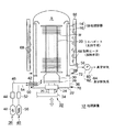
図1は本発明に係るケミカル酸化膜の除去方法を実施するための処理装置の一例を示す構成図である。この処理装置12は、内筒14と外筒16とよりなる石英製の2重管構造の縦型の所定の長さの処理容器18を有している。上記内筒14内の処理空間Sには、被処理体を保持するための支持手段としての石英製のウエハボート20が収容されており、このウエハボート20には被処理体としての半導体ウエハWが所定のピッチで多段に保持される。尚、このピッチは、一定の場合もあるし、ウエハ位置によって異なっている場合もある。
Hereinafter will be described in detail with reference to Kazumi施例the method for removing the chemical oxide film according to the present invention in the accompanying drawings.
FIG. 1 is a block diagram showing an example of a processing apparatus for carrying out the method for removing a chemical oxide film according to the present invention. The processing apparatus 12 includes a
この処理容器18の下方を開閉するためにキャップ22が設けられ、これには磁性流体シール24を介して貫通する回転軸26が設けられる。そして、この回転軸26の上端に回転テーブル28が設けられ、このテーブル28上に保温筒30を設け、この保温筒30上に上記ウエハボート20を載置している。そして、上記回転軸26は昇降可能なボートエレベータ32のアーム34に取り付けられており、上記キャップ22やウエハボート20等と一体的に昇降可能にしており、ウエハボート20は処理容器18内へその下方から挿脱可能になされている。尚、ウエハボート20を回転せずに、これを固定状態としてもよい。
上記処理容器18の下端開口部は、例えばステンレス製のマニホールド36が接合されており、このマニホールド36には、流量制御されたHFガスとNH3 ガスとを処理容器18内へ導入するためのHFガス供給系38とNH3 ガス供給系40がそれぞれ個別に設けられている。
A
A
具体的には、まず、上記HFガス供給系38は、上記マニホールド36を貫通して設けられるHFガスノズル42を有しており、このノズル42には途中に例えばマスフローコントローラのような流量制御器44を介設したガス供給路46が接続される。そして、このガス供給路46には、HFガス源48が接続されている。
また、上記NH3 ガス供給系40は、同様に上記マニホールド36を貫通して設けられるNH3 ガスノズル50を有しており、このノズル50には途中に例えばマスフローコントローラのような流量制御器52を介設したガス供給路54が接続される。そして、このガス供給路54には、NH3 ガス源56が接続されている。
Specifically, first, the HF
Similarly, the NH 3
従って、上記各ノズル42、50より供給された各ガスは、内筒14内の処理空間Sであるウエハの収容領域を上昇して天井部で下方へ折り返し、そして内筒14と外筒16との間隙内を流下して排出されることになる。また、外筒16の底部側壁には、排気口58が設けられており、この排気口58には、排気路60に真空ポンプ62を介設してなる真空排気系64が接続されており、処理容器18内を真空引きするようになっている。
また、処理容器18の外周には、断熱層66が設けられており、この内側には、加熱手段として加熱ヒータ68が設けられて内側に位置するウエハWを所定の温度に加熱するようになっている。ここで、処理容器18の全体の大きさは、例えば成膜すべきウエハWのサイズを8インチ、ウエハボート20に保持されるウエハ枚数を150枚程度(製品ウエハを130枚程度、ダミーウエハ等を20枚程度)とすると、内筒14の直径は略260〜270mm程度、外筒16の直径は略275〜285mm程度、処理容器18の高さは略1280mm程度である。
Accordingly, the gases supplied from the
In addition, a
また、ウエハWのサイズが12インチの場合には、ウエハボート20に保持されるウエハ枚数が25〜50枚程度の場合もあり、この時、内筒14の直径は略380〜420mm程度、外筒16の直径は略440〜500mm程度、処理容器18の高さは略800mm程度である。尚、これらの数値は単に一例を示したに過ぎない。
また上記キャップ22とマニホールド36との間には、ここをシールするOリング等のシール部材70が設けられ、上記マニホールド36の上端部と外筒16の下端部との間には、ここをシールするOリング等のシール部材72が設けられる。尚、図示されていないが、ガス供給系としては不活性ガスとして、例えばN2 ガスを供給するガス供給系も設けられているのは勿論である。
Further, when the size of the wafer W is 12 inches, the number of wafers held in the
Further, a
次に、以上のように構成された処理装置を用いて行なわれる本発明方法について説明する。
ここでは除去するシリコン酸化膜としてケミカル酸化膜(SiO2 )を除去する場合を例にとって説明する。
図2は半導体ウエハの処理工程の一部を示す工程図である。図2(A)に示す半導体ウエハWの表面には、シリコン酸化膜としてケミカル酸化膜4が形成されており、このケミカル酸化膜4の付いたウエハWは、先に図10(A)及び図10(B)を参照して説明したように、ウエハ表面の自然酸化膜2を除去した後、このウエハWの表面にH2 O2 とNH4 OHとの混合溶液を用いたケミカル処理を施すことにより形成される。
Next, the method of the present invention performed using the processing apparatus configured as described above will be described.
Here, a case where a chemical oxide film (SiO 2 ) is removed as a silicon oxide film to be removed will be described as an example.
FIG. 2 is a process diagram showing a part of a semiconductor wafer processing process. On the surface of the semiconductor wafer W shown in FIG. 2 (A), which is chemical oxide film 4 is formed as a silicon oxide film, the wafer W with a the chemical oxide film 4, FIGS. 10 (A) and above As described with reference to FIG. 10 (B ), after removing the natural oxide film 2 on the wafer surface, the surface of the wafer W is subjected to chemical treatment using a mixed solution of H 2 O 2 and NH 4 OH. Is formed.
ここでは、上記ケミカル酸化膜4の付いたウエハWを上記処理装置12内へ収容し、ここでHFガスとNH3 ガスとの混合ガスを用いて、図2(B)に示すように上記ケミカル酸化膜4をエッチングにより除去する。
その後は、他の処理装置で図2(C)に示すように、例えばゲート酸化膜を形成するために熱酸化膜6を形成することになる。尚、後述する実施例では、上記ケミカル酸化膜4の除去処理と上記熱酸化膜6の形成処理とを同一処理装置内で行うことができる。
Here, the wafer W with the chemical oxide film 4 is accommodated in the processing apparatus 12, and a mixed gas of HF gas and NH 3 gas is used here, as shown in FIG. The oxide film 4 is removed by etching.
Thereafter, as shown in FIG. 2C, the
次に、上記処理装置12を用いて行うケミカル酸化膜4の除去処理について具体的に説明する。
まず、図2(A)に示すように表面にケミカル酸化膜4の付いた未処理の多数枚の半導体ウエハWをウエハボート20に所定のピッチで多段に保持させ、この状態でボートエレベータ32を上昇駆動することにより、ウエハボート20を処理容器18内へその下方より挿入し、処理容器18内を密閉する。この処理容器18内は予め、所定の温度に維持されており、また、例えば半導体ウエハWの表面には、上述のようにケミカル酸化膜4が形成されている。上述のようにウエハWが挿入されたならば真空排気系64により処理容器18内を真空引きする。
Next, the removal process of the chemical oxide film 4 performed using the processing apparatus 12 will be specifically described.
First, as shown in FIG. 2A, a large number of unprocessed semiconductor wafers W having a chemical oxide film 4 on the surface are held in a multi-stage at a predetermined pitch on the
そして、これと同時にHFガス供給系38のHFガスノズル42から流量制御されたHFガスを処理容器18内へ導入すると共に、NH3 ガス供給系40のNH3 ガスノズル50から流量制御されたNH3 ガスを処理容器18内へ導入する。
このように、処理容器18内へ別々に導入されたHFガスとNH3 ガスはこの処理容器18内を上昇しつつ混合してこの混合ガスがウエハWに形成されているケミカル酸化膜4をエッチングして除去することができる。
この時のエッチングの処理条件に関しては、処理温度は、室温よりも高くて、例えば100℃〜600℃の範囲内であり、また処理圧力は、処理容器18内の真空引ききり状態、例えば26Pa(0.2Torr)〜53200Pa(400Torr)の範囲内である。
At the same time, the HF gas whose flow rate is controlled from the
As described above, the HF gas and the NH 3 gas separately introduced into the
Regarding the etching processing conditions at this time, the processing temperature is higher than room temperature, for example, within a range of 100 ° C. to 600 ° C. 0.2 Torr) to 53200 Pa (400 Torr).
このように、HF(フッ化水素)ガス単独では処理容器18の温度を室温付近まで低下させないとシリコン酸化膜を除去できなかったが、NH3 (アンモニア)ガスを混合させることにより、処理容器18の温度を室温付近まで低下させることなくシリコン酸化膜、ここではケミカル酸化膜を除去することができ、従って、処理容器18の温度を昇降温させる時間を少なくできるので、スループットを向上させることができる。
As described above, the HF (hydrogen fluoride) gas alone cannot remove the silicon oxide film unless the temperature of the
このようにして、ケミカル酸化膜4の除去されたウエハWは、この処理装置12に熱酸化膜形成用の部材が設けられている場合にはこの処理装置で、上記部材が設けられていない場合には他の処理装置へ搬送されて、図2(C)に示すように例えばゲート酸化膜用の熱酸化膜6が酸化処理により形成されることになる。この場合、前述したように半導体集積回路の高微細化及び高集積化のためにゲート酸化膜の薄膜化が要請されてその目標膜厚値が1.0〜1.2nm程度まで小さくなっても、この熱酸化膜6を膜厚の制御性良く形成することができる。
Thus, the wafer W from which the chemical oxide film 4 has been removed is obtained when the thermal oxide film forming member is provided in the processing apparatus 12 and the above member is not provided in the processing apparatus. As shown in FIG. 2C, for example, a
ここで実際にケミカル酸化膜(SiO2 )の膜厚の変化について評価を行ったので、その評価結果について説明する。図3はケミカル酸化膜の膜厚の変化を示すグラフであり、図中、”TOP”はウエハボート20の上部の位置を示し、”BTM”はウエハボート20の下部の位置を示す。ここでの処理条件は、処理温度が300℃、処理圧力が53200Pa(400Torr)、HFガスの流量が182sccm、NH3 ガスの流量が1820sccm、N2 ガスの流量が8000sccmであり、10分間のエッチング処理を行った。
図3から明らかなように、”TOP”も”BTM”においても、処理前と処理後では膜厚が大きく変化しており、10分間の処理でケミカル酸化膜を厚さ0.39〜0.41nm程度の範囲で削り取ることができることを確認できた。
Here, since the actual change in the thickness of the chemical oxide film (SiO 2 ) was evaluated, the evaluation result will be described. FIG. 3 is a graph showing changes in the film thickness of the chemical oxide film. In the figure, “TOP” indicates the position of the upper portion of the
As is apparent from FIG. 3, the film thickness greatly changes before and after the treatment in both “TOP” and “BTM”, and the chemical oxide film has a thickness of 0.39 to 0. It was confirmed that the material could be scraped off in the range of about 41 nm.
次にNH3 ガスを添加して混合することの有効性について評価を行ったので、その評価結果について説明する。図4はケミカル酸化膜の削れ量のNH3 ガス依存性を示すグラフである。図4中、左側の部分はHFガスのみを用いた場合を示し、右側の部分はHFガスとNH3 ガスとの混合ガスを用いた場合を示す。ここでの処理条件は上記図3にて説明した場合と同じであり、処理温度が300℃、処理圧力が53200Pa(400Torr)、HFガスの流量が182sccm、NH3 ガスの流量が1820sccm、N2 ガスの流量が8000sccmであり、10分間のエッチング処理を行った。
図4から明らかなように、NH3 ガスを添加しないでHFガスのみで処理を行った場合には、ケミカル酸化膜はほとんど削れないのに対して、HFガスとNH3 ガスとの混合ガスを用いた場合には厚さが0.59〜0.61nm程度削り取ることができることが判明した。これにより、NH3 ガスを添加しないとケミカル酸化膜を削れないことが判明した。
Next, since the effectiveness of adding and mixing NH 3 gas was evaluated, the evaluation result will be described. FIG. 4 is a graph showing the NH 3 gas dependency of the amount of abrasion of the chemical oxide film. In FIG. 4, the left part shows a case where only HF gas is used, and the right part shows a case where a mixed gas of HF gas and NH 3 gas is used. The processing conditions here are the same as those described with reference to FIG. 3, the processing temperature is 300 ° C., the processing pressure is 53200 Pa (400 Torr), the flow rate of HF gas is 182 sccm, the flow rate of NH 3 gas is 1820 sccm, and N 2. The gas flow rate was 8000 sccm, and the etching process was performed for 10 minutes.
As is apparent from FIG. 4, when the treatment is performed only with the HF gas without adding the NH 3 gas, the chemical oxide film is hardly scraped, whereas the mixed gas of the HF gas and the NH 3 gas is changed. It has been found that when used, the thickness can be cut off by about 0.59 to 0.61 nm. As a result, it was found that the chemical oxide film could not be removed unless NH 3 gas was added.
次に、ケミカル酸化膜以外の他のシリコン酸化膜やシリコン含有材料との選択性の評価を行ったので、その評価結果について説明する。図5はケミカル酸化膜と、これ以外のシリコン酸化膜やシリコン含有材料との選択性の有無を示すデータである。尚、圧力に関しては1Torr=133Paであり、選択性のある部分には”○”印を付してある。また図5中の”−”はSi材料をオーバーエッチングしており、測定が不可能であることを意味している。
ここでは処理温度を100〜600℃まで変化させており、処理圧力を26Pa(0.2Torr)〜53200Pa(400Torr)まで変化させて、10分間のエッチング処理を行っている。尚、図5中の圧力”VAC”は処理容器18内を真空引きで引ききり状態にした時の圧力を示し、真空ポンプの能力等にもよるが、その時の処理容器18内の圧力は26Pa(0.2Torr)〜40Pa(0.3Torr)程度である。またHFガスとNH3 ガスとの流量比は1:10〜10:1の範囲内で変化させている。この図中の各数値は10分間のエッチング処理によって削り取られた厚さをそれぞれ示しており、その単位はnmである。
Next, since the selectivity with other silicon oxide films and silicon-containing materials other than the chemical oxide film was evaluated, the evaluation results will be described. FIG. 5 is data showing the presence / absence of selectivity between the chemical oxide film and other silicon oxide films and silicon-containing materials. The pressure is 1 Torr = 133 Pa, and the selective portion is marked with “◯”. Further, “-” in FIG. 5 means that Si material is over-etched and measurement is impossible.
Here, the processing temperature is changed from 100 to 600 ° C., the processing pressure is changed from 26 Pa (0.2 Torr) to 53200 Pa (400 Torr), and the etching process is performed for 10 minutes. Note that the pressure “VAC” in FIG. 5 indicates the pressure when the inside of the
ここで評価で用いた材料は、ケミカル酸化膜、シリコン材料(ポリシリコン膜)、シリコン窒化膜(SiN)、ケミカル酸化膜以外のシリコン酸化膜としてはTEOSを用いて形成されたシリコン酸化膜と熱酸化処理によって形成された熱酸化膜が用いられた。
まずケミカル酸化膜について検討すると、処理温度100〜600℃の範囲の全ての領域において、削り取り量の大小はあるが、ケミカル酸化膜を削り取ることができることを確認できた。また同様に処理圧力も”VAC”(0.2Torr)〜400Torrの範囲の全ての領域においてケミカル酸化膜を削り取ることができることを確認できた。特に処理温度が100℃であっても、処理圧力が”VAC”であってNH3 ガスリッチの時にはケミカル酸化膜を削り取ることができる。ただし処理温度が100℃の時で処理圧力が7.6Torr或いは400Torrの場合及び処理温度が300℃で処理圧力が”VAC”の場合には、NH3 ガスがリッチ状態になっていないためにケミカル酸化膜を削り取ることができなかった。尚、処理温度を100℃よりも低い50℃に設定してHFガスとNH3 ガスとの混合ガスによりエッチング処理を行ってみたが、ケミカル酸化膜は全く削れなかった。従って、処理温度は100℃以上であることが必要である。
The material used in the evaluation is a chemical oxide film, a silicon material (polysilicon film), a silicon nitride film (SiN), a silicon oxide film formed using TEOS as a silicon oxide film other than the chemical oxide film, and heat. A thermal oxide film formed by oxidation treatment was used.
First, when the chemical oxide film was examined, it was confirmed that the chemical oxide film could be scraped in all regions within the processing temperature range of 100 to 600 ° C., although the amount of scraping was large. Similarly, it was confirmed that the chemical oxide film could be scraped off in the entire processing pressure range of “VAC” (0.2 Torr) to 400 Torr. In particular, even when the processing temperature is 100 ° C., the chemical oxide film can be scraped off when the processing pressure is “VAC” and the NH 3 gas is rich. However, when the processing temperature is 100 ° C. and the processing pressure is 7.6 Torr or 400 Torr, and when the processing temperature is 300 ° C. and the processing pressure is “VAC”, the NH 3 gas is not in a rich state, so the chemical The oxide film could not be removed. In addition, when the processing temperature was set to 50 ° C. lower than 100 ° C. and etching was performed with a mixed gas of HF gas and NH 3 gas, the chemical oxide film was not scraped at all. Accordingly, the processing temperature needs to be 100 ° C. or higher.
次に、ケミカル酸化膜とポリシリコン(シリコン材料)との選択性について検討する。
図5から明らかなように、ポリシリコンは処理温度が100℃の時は処理圧力が400Torrの場合、及び処理温度が600℃の時は処理圧力が”VAC”〜7.6Torrの圧力範囲で大きく削り取られてしまっている。そして、処理温度が300℃及び400℃の時には、処理圧力が”VAC”〜400Torrの全ての範囲において、またHFガスとNH3 ガスの流量比が10:1〜1:10の全ての範囲において、ポリシリコンの削り取り量は略”0”である。従って、処理温度が300〜400℃の範囲内においては、ポリシリコンに対してケミカル酸化膜を選択的に削り取ることができることが判明する。
Next, the selectivity between the chemical oxide film and polysilicon (silicon material) will be examined.
As is clear from FIG. 5, when polysilicon is processed at a processing temperature of 100 ° C., the processing pressure is 400 Torr, and when the processing temperature is 600 ° C., the processing pressure is large in a pressure range of “VAC” to 7.6 Torr. It has been scraped off. When the processing temperature is 300 ° C. and 400 ° C., the processing pressure is in the whole range of “VAC” to 400 Torr, and the flow rate ratio of HF gas to NH 3 gas is in the whole range of 10: 1 to 1:10. The amount of polysilicon scraped is approximately “0”. Therefore, it is found that the chemical oxide film can be selectively scraped with respect to polysilicon when the processing temperature is in the range of 300 to 400 ° C.
次にケミカル酸化膜とシリコン窒化膜との選択性について検討する。
図5から明らかなように、シリコン窒化膜は、処理温度が100〜600℃の全範囲内で削り取られてしまっているが、処理温度が300℃で処理圧力が7.6Torrの場合、処理温度が400℃で処理圧力が”VAC”及び7.6Torrの場合、処理温度が600℃で処理圧力が”VAC”の場合には、それぞれ削り取り量が、ケミカル酸化膜の削り取り量よりも少なくなっている。従って、処理温度が300〜600℃の範囲で且つ処理圧力が7.6Torr以下の時においては、シリコン窒化膜に対してケミカル酸化膜を選択的に削り取ることができることが判明する。
Next, the selectivity between the chemical oxide film and the silicon nitride film is examined.
As is apparent from FIG. 5, the silicon nitride film has been scraped in the entire processing temperature range of 100 to 600 ° C., but when the processing temperature is 300 ° C. and the processing pressure is 7.6 Torr, the processing temperature When the processing pressure is “VAC” and 7.6 Torr at 400 ° C., when the processing temperature is 600 ° C. and the processing pressure is “VAC”, the scraping amount is smaller than the scraping amount of the chemical oxide film, respectively. Yes. Therefore, it is found that when the processing temperature is in the range of 300 to 600 ° C. and the processing pressure is 7.6 Torr or less, the chemical oxide film can be selectively scraped off from the silicon nitride film.
次にケミカル酸化膜とTEOSにより形成されたシリコン酸化膜との選択性について説明する。
図5から明らかなように、TEOSにより形成されたシリコン酸化膜は、処理温度が100〜600℃の全範囲内で削り取られてしまっているが、処理温度が300℃で処理圧力が7.6Torrの場合、処理温度が400℃で処理圧力が”VAC”及び7.6Torrの場合には、それぞれ削り取り量が、ケミカル酸化膜の削り取り量よりも少なくなっている。従って、処理温度が300〜400℃の範囲内で且つ処理圧力が7.6Torr以下の時においては、TEOSにより形成したシリコン酸化膜に対してケミカル酸化膜を選択的に削り取ることができることが判明する。
Next, the selectivity between the chemical oxide film and the silicon oxide film formed by TEOS will be described.
As is apparent from FIG. 5, the silicon oxide film formed by TEOS has been scraped in the entire processing temperature range of 100 to 600 ° C., but the processing temperature is 300 ° C. and the processing pressure is 7.6 Torr. In this case, when the processing temperature is 400 ° C. and the processing pressure is “VAC” and 7.6 Torr, the scraping amount is smaller than the scraping amount of the chemical oxide film. Therefore, it is found that when the processing temperature is in the range of 300 to 400 ° C. and the processing pressure is 7.6 Torr or less, the chemical oxide film can be selectively scraped with respect to the silicon oxide film formed by TEOS. .
次にケミカル酸化膜と熱酸化処理によって形成された熱酸化膜(SiO2 )との選択性について説明する。
図5から明らかなように、熱酸化処理により形成されたシリコン酸化膜は、処理温度が100〜600℃の全範囲内で削り取られてしまっているが、処理温度が100℃で処理圧力”VAC”の場合、処理温度が300℃で処理圧力が7.6Torr、150Torr、400Torr(NH3 リッチ状態の時)の場合、処理温度が400℃で処理圧力が”VAC”〜400Torrの場合、処理温度が600℃で処理圧力が”VAC”及び7.6Torrの場合には、それぞれ削り取り量が、ケミカル酸化膜の削り取り量よりも少なくなっている。従って処理温度が100〜600℃の全範囲内で熱酸化処理により形成したシリコン酸化膜に対してケミカル酸化膜を選択的に削り取ることができることが判明する。
Next, the selectivity between the chemical oxide film and the thermal oxide film (SiO 2 ) formed by the thermal oxidation process will be described.
As is apparent from FIG. 5, the silicon oxide film formed by the thermal oxidation process has been scraped within the entire processing temperature range of 100 to 600 ° C., but at the processing temperature of 100 ° C., the processing pressure “VAC "In the case of a processing temperature of 300 ° C. and a processing pressure of 7.6 Torr, 150 Torr, 400 Torr (when NH 3 is rich), the processing temperature is 400 ° C. and the processing pressure is“ VAC ”to 400 Torr. Is 600 ° C. and the processing pressure is “VAC” and 7.6 Torr, the amount of scraping is smaller than that of the chemical oxide film, respectively. Therefore, it can be seen that the chemical oxide film can be selectively scraped with respect to the silicon oxide film formed by the thermal oxidation process within the entire processing temperature range of 100 to 600 ° C.
また図5から明らかなように、HFガスとNH3 ガスとの混合ガスによれば、ケミカル酸化膜のみならず、TEOSより形成されたシリコン酸化膜、熱処理により形成されたシリコン酸化膜も削り取ることができるので、他のシリコン酸化膜、例えばシリコン基板上に形成される自然酸化膜や熱CVD処理やプラズマCVD処理によって堆積して形成されるシリコン酸化膜等も削り取ることができる。 As is clear from FIG. 5, according to the mixed gas of HF gas and NH 3 gas, not only the chemical oxide film but also the silicon oxide film formed from TEOS and the silicon oxide film formed by heat treatment are scraped off. Therefore, other silicon oxide films, for example, a natural oxide film formed on a silicon substrate, a silicon oxide film deposited by thermal CVD processing or plasma CVD processing, and the like can be scraped off.
次に、HFガスに対してNH3 ガスが更にリッチな流量比における選択エッチング性について検討したので、その評価結果について説明する。
図6はケミカル酸化膜と、これ以外のシリコン酸化膜やシリコン含有材料との選択性データを示す図、図7は図6のデータを示す棒グラフであり、”TOP”と”BTM”のデータについてそれぞれ示している。
ここでは先に説明した図5に示す場合よりも、NH3 ガスが更にリッチな領域について検討を行っており、具体的にはHFガス:NH3 ガスの流量比が1:10〜1:50の範囲の領域について行っている。ここで、処理温度、処理圧力、処理時間は、図5に示すプロセス条件の中で平均的な値にそれぞれ設定しており、具体的には、処理温度は200℃、処理圧力は150Torr、処理時間は10分にそれぞれ設定している。またプロセスガスについては、NH3 ガスを1820sccmに固定し、HFガスの流量を変化させることによって両ガスの流量比を変化させている。尚、ウエハの処理枚数は150枚である。
Next, since the selective etching property at a flow rate ratio in which the NH 3 gas is richer than the HF gas was examined, the evaluation result will be described.
FIG. 6 is a diagram showing selectivity data between a chemical oxide film and other silicon oxide films and silicon-containing materials, and FIG. 7 is a bar graph showing the data of FIG. 6, with respect to “TOP” and “BTM” data. Each is shown.
Here, the region richer in NH 3 gas than in the case shown in FIG. 5 described above is examined. Specifically, the flow rate ratio of HF gas: NH 3 gas is 1:10 to 1:50. This is done for a range of areas. Here, the processing temperature, processing pressure, and processing time are set to average values in the process conditions shown in FIG. 5, specifically, the processing temperature is 200 ° C., the processing pressure is 150 Torr, the processing Each time is set to 10 minutes. As for the process gas, NH 3 gas is fixed at 1820 sccm, and the flow rate ratio of both gases is changed by changing the flow rate of the HF gas. The number of processed wafers is 150.
図6及び図7から明らかなように、HF:NH3 の流量比を1:10〜1:50まで1:10、1:20、1:50のように変化させても、ポリシリコン膜のエッチング量(削れ量)は略ゼロであって、ほとんど削れていないのに対して、ケミカル酸化膜のエッチング量は0.41〜0.57nmの範囲で安定的に削られており、この点より、上記流量比の全範囲において、ポリシリコン膜に対してケミカル酸化膜を選択的にエッチングできることが確認できた。
またケミカル酸化膜とSiN膜、TEOS膜及び熱酸化膜との間の選択エッチング性について検討すると、TEOS膜は全ての流量比においてケミカル酸化膜のエッチング量よりも多く、しかも激しくエッチングされているが、NH3 リッチの程度が大きくなる程、そのエッチング量は次第に小さくなってきている。
As apparent from FIGS. 6 and 7, even if the flow rate ratio of HF: NH 3 is changed from 1:10 to 1:50, such as 1:10, 1:20, and 1:50, The etching amount (scraping amount) is almost zero and is hardly scraped. On the other hand, the etching amount of the chemical oxide film is stably shaved in the range of 0.41 to 0.57 nm. It was confirmed that the chemical oxide film can be selectively etched with respect to the polysilicon film in the entire range of the flow rate ratio.
Further, when the selective etching property between the chemical oxide film and the SiN film, the TEOS film, and the thermal oxide film is examined, the TEOS film is larger than the etching amount of the chemical oxide film at all flow rate ratios, and is etched intensely. The amount of etching gradually decreases as the degree of NH 3 richness increases.
またSiN膜、熱酸化膜については、HF:NH3 比が1:10の時は、SiN膜と熱酸化膜のエッチング量は、共にケミカル酸化膜のエッチング量と略同じか、或いはこれより多くエッチングされている。しかしながら、HF:NH3 比が1:20の時は、SiN膜と熱酸化膜のエッチング量は、共にケミカル酸化膜のエッチング量よりもかなり少なくなってきており、特に、HF:NH3 比が1:50の時は、SiN膜と熱酸化膜のエッチング量は、共に略ゼロになっている。この結果、SiN膜、TEOS膜、熱酸化膜のエッチングを抑制しつつケミカル酸化膜をできるだけ削るためには、できるだけNH3 ガスをリッチ状態にするのがよく、好ましくは、HF:NH3 比を1:20〜1:50の範囲内に設定するのがよいことが確認できた。 As for the SiN film and the thermal oxide film, when the HF: NH 3 ratio is 1:10, the etching amounts of the SiN film and the thermal oxide film are both approximately equal to or larger than the etching amount of the chemical oxide film. Etched. However, when the HF: NH 3 ratio is 1:20, the etching amounts of the SiN film and the thermal oxide film are both considerably smaller than the etching amount of the chemical oxide film. In particular, the HF: NH 3 ratio is At 1:50, the etching amounts of the SiN film and the thermal oxide film are both substantially zero. As a result, in order to reduce the chemical oxide film as much as possible while suppressing the etching of the SiN film, the TEOS film, and the thermal oxide film, the NH 3 gas should be made as rich as possible, and preferably the HF: NH 3 ratio is increased. It was confirmed that it should be set within the range of 1:20 to 1:50.
尚、図1に示す装置例にあっては、本発明の理解を容易にするために、ガス供給源としてHFガス供給系38とNH3 ガス供給系40を設けた場合を例にとって説明したが、これに限定されず、他の処理に必要とするガス供給源を設けて連続処理を行うようにしてもよい。この一例として図8は水蒸気や水蒸気を形成するためのガスを供給する酸化用ガス供給系を併設した処理装置の構成図を示している。尚、図1に示す構成部分と同一構成部分については同一符号を付してその説明を省略する。
In the example of the apparatus shown in FIG. 1, the case where the HF
図8に示すように、ここではガス供給源として上記HFガス供給系38及びNH3 ガス供給系40に加えて、酸化用ガス供給系80が設けられている。具体的には、この酸化用ガス供給系80としては、H2 ガス源80AとO2 ガス源80Bとをそれぞれ設け、それぞれのガスを流量制御器82A、82Bがそれぞれ介設されたガス流路84A、84Bを介して各ガスノズル86A、86Bより必要に応じて処理容器18内へ導入し得るようになっている。
このようにH2 ガスとO2 ガスとを処理容器18内へ供給することにより、例えばこれらのガスを処理容器18内で燃焼させて水蒸気を発生させ、これにより例えばシリコン基板の表面に熱酸化処理を施して熱酸化膜を形成できるようになっている。
As shown in FIG. 8, here, in addition to the HF
By supplying H 2 gas and O 2 gas into the
従って、図8に示すこの処理装置によれば、最初にHFガスとNH3 ガスとを供給してウエハ表面に付着しているケミカル酸化膜の除去処理を行ってHFガスとNH3 ガスの供給を停止して、次に、連続してH2 ガスとO2 ガスとを供給して水蒸気を発生させることによって熱酸化処理を行って、例えばゲート酸化膜となる熱酸化膜を連続して形成することができる。
尚、上記酸化用ガス供給系80としてH2 ガスとO2 ガスとを燃焼させる外部燃焼装置を設けたり、触媒を利用した水蒸気発生装置を用いて発生した水蒸気を処理容器18内へ導入させるようにしてもよい。
Therefore, according to this processing apparatus shown in FIG. 8, first, HF gas and NH 3 gas are supplied to remove the chemical oxide film adhering to the wafer surface and supply of HF gas and NH 3 gas. Next, a thermal oxidation process is performed by continuously supplying H 2 gas and O 2 gas to generate water vapor to form, for example, a thermal oxide film that becomes a gate oxide film. can do.
It is to be noted that an external combustion device for combusting H 2 gas and O 2 gas is provided as the oxidizing
また他の一例として図9はシリコン膜形成用のガスを供給するシリコン膜形成用ガス供給系を併設した処理装置の構成図を示している。尚、図1に示す構成部分と同一構成部分については同一符号を付してその説明を省略する。
図9に示すように、ここではガス供給源として上記HFガス供給系38及びNH3 ガス供給系40に加えて、シリコン膜形成用ガス供給系90が設けられている。具体的には、このシリコン膜形成用ガス供給系90としては、モノシラン(SiH4 )ガス源90Aを設け、このガスを流量制御器92Aが介設されたガス流路94Aを介してガスノズル96Aより必要に応じて処理容器18内へ導入し得るようになっている。
また同時にドーパント(不純物)を導入するためにドーパントガス源として例えばモノゲルマル(GeH4 )ガス源90Bが設けられており、このガスを流量制御器92Bが介設されたガス流路94Bを介してガスノズル96Bより必要に応じて処理容器18内へ導入し得るようになっている。
As another example, FIG. 9 shows a block diagram of a processing apparatus provided with a silicon film forming gas supply system for supplying a gas for forming a silicon film. The same components as those shown in FIG. 1 are denoted by the same reference numerals, and the description thereof is omitted.
As shown in FIG. 9, here, in addition to the HF
At the same time, for example, a monogermal (GeH 4 ) gas source 90B is provided as a dopant gas source in order to introduce a dopant (impurity), and this gas is supplied to a gas nozzle 94B through a gas flow path 94B provided with a flow rate controller 92B. 96B can be introduced into the
このようにモノシランとモノゲルマルを処理容器18内へ供給することにより、ドーパントとしてゲルマニウムが導入されたシリコン膜(ポリシリコン膜)を形成することができるようになっている。
従って、図9に示すこの処理装置によれば、最初にHFガスとNH3 ガスとを供給してウエハ表面に付着しているケミカル酸化膜の除去処理を行ってHFガスとNH3 ガスの供給を停止して、次に、連続してモノシランガスとモノゲルマルガスとを供給して不純物としてゲルマニウムが導入されたシリコン膜を連続して形成することができる。またこの場合、温度を適宜選択することにより、ゲルマニウムがドープされたエピタキシャル膜も形成することができる。更に図8及び図9に示す装置構成を組み合わせることにより、ケミカル酸化膜除去処理後にゲート酸化膜の形成及びシリコンゲート電極の形成を連続処理できる装置構成とすることもできる。
Thus, by supplying monosilane and monogermale into the
Therefore, according to this processing apparatus shown in FIG. 9, first, HF gas and NH 3 gas are supplied to perform removal processing of the chemical oxide film adhering to the wafer surface, and supply of HF gas and NH 3 gas. Then, a silicon film in which germanium is introduced as an impurity can be continuously formed by continuously supplying monosilane gas and monogermal gas. In this case, an epitaxial film doped with germanium can also be formed by appropriately selecting the temperature. Further, by combining the apparatus configurations shown in FIGS. 8 and 9, it is possible to form an apparatus configuration capable of continuously processing the formation of the gate oxide film and the formation of the silicon gate electrode after the chemical oxide film removal process.
ここではケミカル酸化膜を除去した後に熱酸化膜やゲルマニウムが導入されたシリコン膜を連続して形成する場合を例にとって説明したが、ケミカル酸化膜を除去した後に、金属膜や窒化膜や他の絶縁膜を形成するようにしてもよい。またこの場合、前述したように、ケミカル酸化膜ではなく、前述したように例えば自然酸化膜を本発明方法により除去した後に、上記したような連続処理を行ってもよい。
尚、上記実施例では2重管構造の処理装置を例にとって説明したが、これは単に一例を示したに過ぎず、例えば単管構造の処理装置にも本発明を適用でき、この場合には処理容器の下方から或いは上方から各ガスを導入して、上方より、或いは下方より処理容器内を真空引きするように構成する。
In this example, the case where a thermal oxide film or a silicon film into which germanium is introduced is continuously formed after the chemical oxide film is removed has been described as an example. However, after the chemical oxide film is removed, a metal film, a nitride film, or another film is formed. An insulating film may be formed. In this case, as described above, instead of the chemical oxide film, for example, the natural oxide film may be removed by the method of the present invention as described above, and then the above-described continuous treatment may be performed.
In the above embodiment, the processing apparatus having a double-pipe structure has been described as an example. However, this is merely an example. For example, the present invention can be applied to a processing apparatus having a single-pipe structure. Each gas is introduced from below or above the processing vessel, and the inside of the processing vessel is evacuated from above or below.
また、本発明方法は上述したような一度に多数枚の半導体ウエハについて酸化処理できるバッチ式の処理装置に限定されず、処理容器内の載置台(支持手段)に半導体ウエハを載置して加熱手段としてランプ加熱或いはヒータ加熱により一枚ずつ酸化処理する枚葉式の処理装置にも適用することができる。
また、被処理体としては、半導体ウエハに限定されず、LCD基板、ガラス基板等にも適用することができる。
Further, the method of the present invention is not limited to the batch type processing apparatus that can oxidize a large number of semiconductor wafers at a time as described above. As a means, the present invention can also be applied to a single-wafer processing apparatus that performs oxidation processing one by one by lamp heating or heater heating.
Further, the object to be processed is not limited to a semiconductor wafer, and can be applied to an LCD substrate, a glass substrate, and the like.
2 自然酸化膜
4 ケミカル酸化膜
6 熱酸化膜
12 処理装置
18 処理容器
20 ウエハボート(支持棚)
38 HFガス供給系
40 NH3 ガス供給系
48 HFガス源
56 NH3 ガス源
68 加熱ヒータ(加熱手段)
80 酸化用ガス供給系
90 シリコン膜形成用ガス供給系
W 半導体ウエハ(被処理体)
2 Natural oxide film 4
38 HF
80 Gas supply system for
Claims (4)
HFガスとNH3 ガスとの混合ガスを用いると共に、シリコン材料に対する前記ケミカル酸化膜の選択性を得るために処理温度は200℃〜400℃の範囲内に設定されて、
処理圧力は26Pa(0.2Torr)〜53200Pa(400Torr)の範囲内に設定され、更に前記HFガスとNH3 ガスとの流量比は、10:1〜1:50の範囲内に設定されて前記ケミカル酸化膜を除去するようにしたことを特徴とするケミカル酸化膜の除去方法。 A silicon oxide film formed on the surface of an object to be processed in a processing container that can be evacuated, and formed by chemical treatment using a mixed solution of H 2 O 2 and NH 4 OH. In the removal method for removing the chemical oxide film,
While using a mixed gas of HF gas and NH 3 gas, the processing temperature is set in the range of 200 ° C. to 400 ° C. in order to obtain the selectivity of the chemical oxide film with respect to the silicon material,
The processing pressure is set in the range of 26 Pa (0.2 Torr) to 53200 Pa (400 Torr), and the flow rate ratio of the HF gas to NH 3 gas is set in the range of 10: 1 to 1:50. A method for removing a chemical oxide film, wherein the chemical oxide film is removed.
HFガスとNH3 ガスとの混合ガスを用いると共に、シリコン窒化膜に対する前記ケミカル酸化膜の選択性を得るために処理温度は200℃〜600℃の範囲内に設定されて、
処理圧力は53200Pa(400Torr)以下に設定され、更に前記HFガスとNH3 ガスとの流量比は1:10〜1:50の範囲内に設定されて前記ケミカル酸化膜を除去するようにしたことを特徴とするケミカル酸化膜の除去方法。 A silicon oxide film formed on the surface of an object to be processed in a processing container that can be evacuated, and formed by chemical treatment using a mixed solution of H 2 O 2 and NH 4 OH. In the removal method for removing the chemical oxide film,
While using a mixed gas of HF gas and NH 3 gas, the processing temperature is set in the range of 200 ° C. to 600 ° C. in order to obtain the selectivity of the chemical oxide film with respect to the silicon nitride film,
The processing pressure is set to 53200 Pa (400 Torr) or lower, and the flow rate ratio of the HF gas to NH 3 gas is set within the range of 1:10 to 1:50 to remove the chemical oxide film. A method for removing a chemical oxide film characterized by the following.
HFガスとNH3 ガスとの混合ガスを用いると共に、CVD(Chemical Vapor Deposition)により形成されたシリコン酸化膜に対する前記ケミカル酸化膜の選択性を得るために処理温度は200℃〜400℃の範囲内に設定され、
処理圧力は53200Pa(400Torr)以下に設定され、更に前記HFガスとNH3 ガスとの流量比は1:10〜1:50の範囲内に設定されて前記ケミカル酸化膜を除去するようにしたことを特徴とするケミカル酸化膜の除去方法。 A silicon oxide film formed on the surface of an object to be processed in a processing container that can be evacuated, and formed by chemical treatment using a mixed solution of H 2 O 2 and NH 4 OH. In the removal method for removing the chemical oxide film,
In order to obtain the selectivity of the chemical oxide film with respect to the silicon oxide film formed by CVD (Chemical Vapor Deposition) using a mixed gas of HF gas and NH 3 gas, the processing temperature is in the range of 200 ° C. to 400 ° C. Set to
The processing pressure is set to 53200 Pa (400 Torr) or lower, and the flow rate ratio of the HF gas to NH 3 gas is set within the range of 1:10 to 1:50 to remove the chemical oxide film. A method for removing a chemical oxide film characterized by the following.
HFガスとNH3 ガスとの混合ガスを用いると共に、熱酸化膜に対する前記ケミカル酸化膜の選択性を得るために処理温度は100℃〜600℃の範囲内に設定され、
処理圧力は53200Pa(400Torr)以下に設定され、更に前記HFガスとNH3 ガスとの流量比は1:10〜1:50の範囲内に設定されて前記ケミカル酸化膜を除去するようにしたことを特徴とするケミカル酸化膜の除去方法。 A silicon oxide film formed on the surface of an object to be processed in a processing container that can be evacuated, and formed by chemical treatment using a mixed solution of H 2 O 2 and NH 4 OH. In the removal method for removing the chemical oxide film,
While using a mixed gas of HF gas and NH 3 gas, in order to obtain the selectivity of the chemical oxide film with respect to the thermal oxide film, the processing temperature is set within a range of 100 ° C. to 600 ° C.,
The processing pressure is set to 53200 Pa (400 Torr) or lower, and the flow rate ratio of the HF gas to NH 3 gas is set within the range of 1:10 to 1:50 to remove the chemical oxide film. dividing removed by the method of chemical oxide film according to claim.
Priority Applications (1)
| Application Number | Priority Date | Filing Date | Title |
|---|---|---|---|
| JP2004124095A JP4039385B2 (en) | 2003-04-22 | 2004-04-20 | Removal method of chemical oxide film |
Applications Claiming Priority (2)
| Application Number | Priority Date | Filing Date | Title |
|---|---|---|---|
| JP2003117664 | 2003-04-22 | ||
| JP2004124095A JP4039385B2 (en) | 2003-04-22 | 2004-04-20 | Removal method of chemical oxide film |
Publications (3)
| Publication Number | Publication Date |
|---|---|
| JP2004343094A JP2004343094A (en) | 2004-12-02 |
| JP2004343094A5 JP2004343094A5 (en) | 2005-08-11 |
| JP4039385B2 true JP4039385B2 (en) | 2008-01-30 |
Family
ID=33543141
Family Applications (1)
| Application Number | Title | Priority Date | Filing Date |
|---|---|---|---|
| JP2004124095A Expired - Fee Related JP4039385B2 (en) | 2003-04-22 | 2004-04-20 | Removal method of chemical oxide film |
Country Status (1)
| Country | Link |
|---|---|
| JP (1) | JP4039385B2 (en) |
Families Citing this family (14)
| Publication number | Priority date | Publication date | Assignee | Title |
|---|---|---|---|---|
| JP4895256B2 (en) * | 2005-02-23 | 2012-03-14 | 東京エレクトロン株式会社 | Substrate surface treatment method |
| JP5046506B2 (en) * | 2005-10-19 | 2012-10-10 | 東京エレクトロン株式会社 | Substrate processing apparatus, substrate processing method, program, and recording medium recording program |
| US20100216296A1 (en) * | 2005-10-27 | 2010-08-26 | Yusuke Muraki | Processing Method and Recording Medium |
| JP4976002B2 (en) * | 2005-11-08 | 2012-07-18 | 東京エレクトロン株式会社 | Substrate processing apparatus, substrate processing method, and recording medium |
| JP4946017B2 (en) * | 2005-11-25 | 2012-06-06 | ソニー株式会社 | Manufacturing method of semiconductor device |
| JP4890025B2 (en) * | 2005-12-28 | 2012-03-07 | 東京エレクトロン株式会社 | Etching method and recording medium |
| JP5119604B2 (en) * | 2006-03-16 | 2013-01-16 | ソニー株式会社 | Manufacturing method of semiconductor device |
| JP2007311376A (en) * | 2006-05-16 | 2007-11-29 | Sony Corp | Manufacturing method of semiconductor device |
| JP5158068B2 (en) | 2009-02-20 | 2013-03-06 | 東京エレクトロン株式会社 | Vertical heat treatment apparatus and heat treatment method |
| JP5661523B2 (en) * | 2011-03-18 | 2015-01-28 | 東京エレクトロン株式会社 | Film forming method and film forming apparatus |
| US9023734B2 (en) * | 2012-09-18 | 2015-05-05 | Applied Materials, Inc. | Radical-component oxide etch |
| JP6726610B2 (en) * | 2016-12-13 | 2020-07-22 | 東京エレクトロン株式会社 | Etching method and substrate processing system |
| JP7407162B2 (en) | 2021-11-17 | 2023-12-28 | 株式会社アルバック | Etching method and etching device |
| JP2023179001A (en) | 2022-06-07 | 2023-12-19 | 東京エレクトロン株式会社 | Substrate processing method and substrate processing apparatus |
-
2004
- 2004-04-20 JP JP2004124095A patent/JP4039385B2/en not_active Expired - Fee Related
Also Published As
| Publication number | Publication date |
|---|---|
| JP2004343094A (en) | 2004-12-02 |
Similar Documents
| Publication | Publication Date | Title |
|---|---|---|
| KR101046523B1 (en) | Removal method of chemical oxide | |
| KR101014062B1 (en) | Film forming method and film forming apparatus | |
| TWI815898B (en) | Etching method and etching device | |
| KR100861851B1 (en) | Method and apparatus for forming silicon oxide film | |
| JP2632262B2 (en) | Method for removing native oxide film in contact hole on silicon wafer | |
| JP4039385B2 (en) | Removal method of chemical oxide film | |
| JP2007516599A (en) | Surface preparation before deposition on germanium | |
| JP2001244214A (en) | Method of manufacturing semiconductor element provided with silicide film | |
| JP2009246340A (en) | Metal smearing reduction method of deposition device, method of manufacturing semiconductor device, storage medium, and deposition device | |
| JP2010219494A (en) | Vertical heat processing device and heat processing method | |
| JP4624207B2 (en) | Film forming method and film forming apparatus | |
| JPWO2004027849A1 (en) | Semiconductor device manufacturing method and substrate processing apparatus | |
| KR102306488B1 (en) | Etching method and etching apparatus | |
| WO2014192870A1 (en) | Substrate processing apparatus, semiconductor device manufacturing method, and substrate processing method | |
| WO2020189288A1 (en) | Film formation method and film formation apparatus | |
| JP3578155B2 (en) | Oxidation method of the object | |
| JP4851647B2 (en) | In situ growth of oxide and silicon layers | |
| JP2021057439A (en) | Deposition method and deposition apparatus | |
| JP2001250818A (en) | Oxidization system and its cleaning method | |
| KR102651431B1 (en) | Film formation method and film formation equipment | |
| JP4490760B2 (en) | Semiconductor device manufacturing method and substrate processing apparatus | |
| JP4112591B2 (en) | Semiconductor device manufacturing method and substrate processing apparatus | |
| JP2006294953A (en) | Method and apparatus for manufacturing semiconductor device | |
| JPH06302566A (en) | Method and apparatus for manufacturing semiconductor device | |
| JP2004343095A (en) | Cleaning method of heat processing equipment |
Legal Events
| Date | Code | Title | Description |
|---|---|---|---|
| A521 | Request for written amendment filed |
Free format text: JAPANESE INTERMEDIATE CODE: A523 Effective date: 20050322 |
|
| A621 | Written request for application examination |
Free format text: JAPANESE INTERMEDIATE CODE: A621 Effective date: 20050322 |
|
| A977 | Report on retrieval |
Free format text: JAPANESE INTERMEDIATE CODE: A971007 Effective date: 20070125 |
|
| A131 | Notification of reasons for refusal |
Free format text: JAPANESE INTERMEDIATE CODE: A131 Effective date: 20070206 |
|
| A521 | Request for written amendment filed |
Free format text: JAPANESE INTERMEDIATE CODE: A523 Effective date: 20070322 |
|
| A131 | Notification of reasons for refusal |
Free format text: JAPANESE INTERMEDIATE CODE: A131 Effective date: 20070424 |
|
| A521 | Request for written amendment filed |
Free format text: JAPANESE INTERMEDIATE CODE: A523 Effective date: 20070612 |
|
| A131 | Notification of reasons for refusal |
Free format text: JAPANESE INTERMEDIATE CODE: A131 Effective date: 20070717 |
|
| A521 | Request for written amendment filed |
Free format text: JAPANESE INTERMEDIATE CODE: A523 Effective date: 20070913 |
|
| TRDD | Decision of grant or rejection written | ||
| A01 | Written decision to grant a patent or to grant a registration (utility model) |
Free format text: JAPANESE INTERMEDIATE CODE: A01 Effective date: 20071016 |
|
| A61 | First payment of annual fees (during grant procedure) |
Free format text: JAPANESE INTERMEDIATE CODE: A61 Effective date: 20071029 |
|
| FPAY | Renewal fee payment (event date is renewal date of database) |
Free format text: PAYMENT UNTIL: 20101116 Year of fee payment: 3 |
|
| R150 | Certificate of patent or registration of utility model |
Ref document number: 4039385 Country of ref document: JP Free format text: JAPANESE INTERMEDIATE CODE: R150 Free format text: JAPANESE INTERMEDIATE CODE: R150 |
|
| FPAY | Renewal fee payment (event date is renewal date of database) |
Free format text: PAYMENT UNTIL: 20101116 Year of fee payment: 3 |
|
| FPAY | Renewal fee payment (event date is renewal date of database) |
Free format text: PAYMENT UNTIL: 20131116 Year of fee payment: 6 |
|
| R250 | Receipt of annual fees |
Free format text: JAPANESE INTERMEDIATE CODE: R250 |
|
| R250 | Receipt of annual fees |
Free format text: JAPANESE INTERMEDIATE CODE: R250 |
|
| R250 | Receipt of annual fees |
Free format text: JAPANESE INTERMEDIATE CODE: R250 |
|
| R250 | Receipt of annual fees |
Free format text: JAPANESE INTERMEDIATE CODE: R250 |
|
| R250 | Receipt of annual fees |
Free format text: JAPANESE INTERMEDIATE CODE: R250 |
|
| R250 | Receipt of annual fees |
Free format text: JAPANESE INTERMEDIATE CODE: R250 |
|
| LAPS | Cancellation because of no payment of annual fees |