JP4976002B2 - Substrate processing apparatus, substrate processing method, and recording medium - Google Patents
Substrate processing apparatus, substrate processing method, and recording medium Download PDFInfo
- Publication number
- JP4976002B2 JP4976002B2 JP2005323329A JP2005323329A JP4976002B2 JP 4976002 B2 JP4976002 B2 JP 4976002B2 JP 2005323329 A JP2005323329 A JP 2005323329A JP 2005323329 A JP2005323329 A JP 2005323329A JP 4976002 B2 JP4976002 B2 JP 4976002B2
- Authority
- JP
- Japan
- Prior art keywords
- substrate
- processing
- processing chamber
- temperature
- wafer
- Prior art date
- Legal status (The legal status is an assumption and is not a legal conclusion. Google has not performed a legal analysis and makes no representation as to the accuracy of the status listed.)
- Active
Links
- 238000012545 processing Methods 0.000 title claims description 260
- 239000000758 substrate Substances 0.000 title claims description 109
- 238000003672 processing method Methods 0.000 title claims description 21
- 239000007789 gas Substances 0.000 claims description 81
- 238000000034 method Methods 0.000 claims description 48
- 230000008569 process Effects 0.000 claims description 44
- QGZKDVFQNNGYKY-UHFFFAOYSA-N Ammonia Chemical compound N QGZKDVFQNNGYKY-UHFFFAOYSA-N 0.000 claims description 31
- 230000007246 mechanism Effects 0.000 claims description 30
- KRHYYFGTRYWZRS-UHFFFAOYSA-N Fluorane Chemical compound F KRHYYFGTRYWZRS-UHFFFAOYSA-N 0.000 claims description 25
- 229910000040 hydrogen fluoride Inorganic materials 0.000 claims description 25
- 239000007795 chemical reaction product Substances 0.000 claims description 18
- VYPSYNLAJGMNEJ-UHFFFAOYSA-N Silicium dioxide Chemical compound O=[Si]=O VYPSYNLAJGMNEJ-UHFFFAOYSA-N 0.000 claims description 17
- 238000010438 heat treatment Methods 0.000 claims description 11
- 239000011261 inert gas Substances 0.000 claims description 11
- 235000012239 silicon dioxide Nutrition 0.000 claims description 8
- 239000000377 silicon dioxide Substances 0.000 claims description 8
- 230000001131 transforming effect Effects 0.000 claims description 3
- 235000012431 wafers Nutrition 0.000 description 155
- 239000010410 layer Substances 0.000 description 72
- 238000012546 transfer Methods 0.000 description 43
- XKRFYHLGVUSROY-UHFFFAOYSA-N Argon Chemical compound [Ar] XKRFYHLGVUSROY-UHFFFAOYSA-N 0.000 description 26
- IJGRMHOSHXDMSA-UHFFFAOYSA-N Atomic nitrogen Chemical compound N#N IJGRMHOSHXDMSA-UHFFFAOYSA-N 0.000 description 16
- 229910001873 dinitrogen Inorganic materials 0.000 description 16
- 239000007788 liquid Substances 0.000 description 14
- 229910021420 polycrystalline silicon Inorganic materials 0.000 description 14
- 229910052786 argon Inorganic materials 0.000 description 13
- 229910000577 Silicon-germanium Inorganic materials 0.000 description 10
- BOTDANWDWHJENH-UHFFFAOYSA-N Tetraethyl orthosilicate Chemical compound CCO[Si](OCC)(OCC)OCC BOTDANWDWHJENH-UHFFFAOYSA-N 0.000 description 7
- 229910052736 halogen Inorganic materials 0.000 description 7
- 150000002367 halogens Chemical class 0.000 description 7
- 239000002245 particle Substances 0.000 description 7
- 238000005530 etching Methods 0.000 description 6
- 229910052782 aluminium Inorganic materials 0.000 description 5
- XAGFODPZIPBFFR-UHFFFAOYSA-N aluminium Chemical compound [Al] XAGFODPZIPBFFR-UHFFFAOYSA-N 0.000 description 5
- 238000001312 dry etching Methods 0.000 description 4
- 239000002923 metal particle Substances 0.000 description 4
- 229910004298 SiO 2 Inorganic materials 0.000 description 3
- -1 ammonium fluorosilicate Chemical compound 0.000 description 3
- 238000006243 chemical reaction Methods 0.000 description 3
- 239000001307 helium Substances 0.000 description 3
- 229910052734 helium Inorganic materials 0.000 description 3
- SWQJXJOGLNCZEY-UHFFFAOYSA-N helium atom Chemical compound [He] SWQJXJOGLNCZEY-UHFFFAOYSA-N 0.000 description 3
- 239000011810 insulating material Substances 0.000 description 3
- 230000002093 peripheral effect Effects 0.000 description 3
- 239000004065 semiconductor Substances 0.000 description 3
- 238000004381 surface treatment Methods 0.000 description 3
- XUIMIQQOPSSXEZ-UHFFFAOYSA-N Silicon Chemical compound [Si] XUIMIQQOPSSXEZ-UHFFFAOYSA-N 0.000 description 2
- DIZPMCHEQGEION-UHFFFAOYSA-H aluminium sulfate (anhydrous) Chemical compound [Al+3].[Al+3].[O-]S([O-])(=O)=O.[O-]S([O-])(=O)=O.[O-]S([O-])(=O)=O DIZPMCHEQGEION-UHFFFAOYSA-H 0.000 description 2
- 238000013459 approach Methods 0.000 description 2
- 230000015572 biosynthetic process Effects 0.000 description 2
- 238000004891 communication Methods 0.000 description 2
- PMHQVHHXPFUNSP-UHFFFAOYSA-M copper(1+);methylsulfanylmethane;bromide Chemical compound Br[Cu].CSC PMHQVHHXPFUNSP-UHFFFAOYSA-M 0.000 description 2
- 238000000151 deposition Methods 0.000 description 2
- 230000008021 deposition Effects 0.000 description 2
- 229910052710 silicon Inorganic materials 0.000 description 2
- 239000010703 silicon Substances 0.000 description 2
- 239000007787 solid Substances 0.000 description 2
- 239000000126 substance Substances 0.000 description 2
- 238000001089 thermophoresis Methods 0.000 description 2
- 230000008016 vaporization Effects 0.000 description 2
- 229910052724 xenon Inorganic materials 0.000 description 2
- FHNFHKCVQCLJFQ-UHFFFAOYSA-N xenon atom Chemical compound [Xe] FHNFHKCVQCLJFQ-UHFFFAOYSA-N 0.000 description 2
- 229910000838 Al alloy Inorganic materials 0.000 description 1
- UFHFLCQGNIYNRP-UHFFFAOYSA-N Hydrogen Chemical compound [H][H] UFHFLCQGNIYNRP-UHFFFAOYSA-N 0.000 description 1
- 229910021529 ammonia Inorganic materials 0.000 description 1
- 238000007743 anodising Methods 0.000 description 1
- QVGXLLKOCUKJST-UHFFFAOYSA-N atomic oxygen Chemical compound [O] QVGXLLKOCUKJST-UHFFFAOYSA-N 0.000 description 1
- 239000000919 ceramic Substances 0.000 description 1
- 230000008859 change Effects 0.000 description 1
- 230000001276 controlling effect Effects 0.000 description 1
- 238000009792 diffusion process Methods 0.000 description 1
- 238000007599 discharging Methods 0.000 description 1
- 230000000694 effects Effects 0.000 description 1
- 238000003682 fluorination reaction Methods 0.000 description 1
- 230000006870 function Effects 0.000 description 1
- 239000011521 glass Substances 0.000 description 1
- 239000012212 insulator Substances 0.000 description 1
- 239000011229 interlayer Substances 0.000 description 1
- 238000004519 manufacturing process Methods 0.000 description 1
- 239000000463 material Substances 0.000 description 1
- 230000001404 mediated effect Effects 0.000 description 1
- 229910052751 metal Inorganic materials 0.000 description 1
- 239000002184 metal Substances 0.000 description 1
- 239000000203 mixture Substances 0.000 description 1
- 238000012986 modification Methods 0.000 description 1
- 230000004048 modification Effects 0.000 description 1
- 230000003287 optical effect Effects 0.000 description 1
- 239000001301 oxygen Substances 0.000 description 1
- 229910052760 oxygen Inorganic materials 0.000 description 1
- 230000001737 promoting effect Effects 0.000 description 1
- 239000012495 reaction gas Substances 0.000 description 1
- 230000001105 regulatory effect Effects 0.000 description 1
- 238000002230 thermal chemical vapour deposition Methods 0.000 description 1
- 230000007723 transport mechanism Effects 0.000 description 1
- 238000011144 upstream manufacturing Methods 0.000 description 1
- 238000009834 vaporization Methods 0.000 description 1
- XLYOFNOQVPJJNP-UHFFFAOYSA-N water Substances O XLYOFNOQVPJJNP-UHFFFAOYSA-N 0.000 description 1
Images


Classifications
-
- H—ELECTRICITY
- H01—ELECTRIC ELEMENTS
- H01L—SEMICONDUCTOR DEVICES NOT COVERED BY CLASS H10
- H01L21/00—Processes or apparatus adapted for the manufacture or treatment of semiconductor or solid state devices or of parts thereof
- H01L21/67—Apparatus specially adapted for handling semiconductor or electric solid state devices during manufacture or treatment thereof; Apparatus specially adapted for handling wafers during manufacture or treatment of semiconductor or electric solid state devices or components ; Apparatus not specifically provided for elsewhere
- H01L21/67005—Apparatus not specifically provided for elsewhere
- H01L21/67011—Apparatus for manufacture or treatment
- H01L21/67155—Apparatus for manufacturing or treating in a plurality of work-stations
- H01L21/67161—Apparatus for manufacturing or treating in a plurality of work-stations characterized by the layout of the process chambers
-
- H—ELECTRICITY
- H01—ELECTRIC ELEMENTS
- H01L—SEMICONDUCTOR DEVICES NOT COVERED BY CLASS H10
- H01L21/00—Processes or apparatus adapted for the manufacture or treatment of semiconductor or solid state devices or of parts thereof
- H01L21/02—Manufacture or treatment of semiconductor devices or of parts thereof
- H01L21/04—Manufacture or treatment of semiconductor devices or of parts thereof the devices having at least one potential-jump barrier or surface barrier, e.g. PN junction, depletion layer or carrier concentration layer
- H01L21/18—Manufacture or treatment of semiconductor devices or of parts thereof the devices having at least one potential-jump barrier or surface barrier, e.g. PN junction, depletion layer or carrier concentration layer the devices having semiconductor bodies comprising elements of Group IV of the Periodic System or AIIIBV compounds with or without impurities, e.g. doping materials
- H01L21/30—Treatment of semiconductor bodies using processes or apparatus not provided for in groups H01L21/20 - H01L21/26
- H01L21/302—Treatment of semiconductor bodies using processes or apparatus not provided for in groups H01L21/20 - H01L21/26 to change their surface-physical characteristics or shape, e.g. etching, polishing, cutting
- H01L21/306—Chemical or electrical treatment, e.g. electrolytic etching
- H01L21/3065—Plasma etching; Reactive-ion etching
-
- H—ELECTRICITY
- H01—ELECTRIC ELEMENTS
- H01L—SEMICONDUCTOR DEVICES NOT COVERED BY CLASS H10
- H01L21/00—Processes or apparatus adapted for the manufacture or treatment of semiconductor or solid state devices or of parts thereof
- H01L21/67—Apparatus specially adapted for handling semiconductor or electric solid state devices during manufacture or treatment thereof; Apparatus specially adapted for handling wafers during manufacture or treatment of semiconductor or electric solid state devices or components ; Apparatus not specifically provided for elsewhere
- H01L21/67005—Apparatus not specifically provided for elsewhere
- H01L21/67011—Apparatus for manufacture or treatment
- H01L21/67098—Apparatus for thermal treatment
- H01L21/67109—Apparatus for thermal treatment mainly by convection
-
- H—ELECTRICITY
- H01—ELECTRIC ELEMENTS
- H01L—SEMICONDUCTOR DEVICES NOT COVERED BY CLASS H10
- H01L21/00—Processes or apparatus adapted for the manufacture or treatment of semiconductor or solid state devices or of parts thereof
- H01L21/67—Apparatus specially adapted for handling semiconductor or electric solid state devices during manufacture or treatment thereof; Apparatus specially adapted for handling wafers during manufacture or treatment of semiconductor or electric solid state devices or components ; Apparatus not specifically provided for elsewhere
- H01L21/67005—Apparatus not specifically provided for elsewhere
- H01L21/67011—Apparatus for manufacture or treatment
- H01L21/67155—Apparatus for manufacturing or treating in a plurality of work-stations
- H01L21/67236—Apparatus for manufacturing or treating in a plurality of work-stations the substrates being processed being not semiconductor wafers, e.g. leadframes or chips
-
- H—ELECTRICITY
- H01—ELECTRIC ELEMENTS
- H01L—SEMICONDUCTOR DEVICES NOT COVERED BY CLASS H10
- H01L21/00—Processes or apparatus adapted for the manufacture or treatment of semiconductor or solid state devices or of parts thereof
- H01L21/67—Apparatus specially adapted for handling semiconductor or electric solid state devices during manufacture or treatment thereof; Apparatus specially adapted for handling wafers during manufacture or treatment of semiconductor or electric solid state devices or components ; Apparatus not specifically provided for elsewhere
- H01L21/683—Apparatus specially adapted for handling semiconductor or electric solid state devices during manufacture or treatment thereof; Apparatus specially adapted for handling wafers during manufacture or treatment of semiconductor or electric solid state devices or components ; Apparatus not specifically provided for elsewhere for supporting or gripping
- H01L21/687—Apparatus specially adapted for handling semiconductor or electric solid state devices during manufacture or treatment thereof; Apparatus specially adapted for handling wafers during manufacture or treatment of semiconductor or electric solid state devices or components ; Apparatus not specifically provided for elsewhere for supporting or gripping using mechanical means, e.g. chucks, clamps or pinches
- H01L21/68714—Apparatus specially adapted for handling semiconductor or electric solid state devices during manufacture or treatment thereof; Apparatus specially adapted for handling wafers during manufacture or treatment of semiconductor or electric solid state devices or components ; Apparatus not specifically provided for elsewhere for supporting or gripping using mechanical means, e.g. chucks, clamps or pinches the wafers being placed on a susceptor, stage or support
- H01L21/6875—Apparatus specially adapted for handling semiconductor or electric solid state devices during manufacture or treatment thereof; Apparatus specially adapted for handling wafers during manufacture or treatment of semiconductor or electric solid state devices or components ; Apparatus not specifically provided for elsewhere for supporting or gripping using mechanical means, e.g. chucks, clamps or pinches the wafers being placed on a susceptor, stage or support characterised by a plurality of individual support members, e.g. support posts or protrusions
-
- H—ELECTRICITY
- H01—ELECTRIC ELEMENTS
- H01L—SEMICONDUCTOR DEVICES NOT COVERED BY CLASS H10
- H01L29/00—Semiconductor devices adapted for rectifying, amplifying, oscillating or switching, or capacitors or resistors with at least one potential-jump barrier or surface barrier, e.g. PN junction depletion layer or carrier concentration layer; Details of semiconductor bodies or of electrodes thereof ; Multistep manufacturing processes therefor
- H01L29/66—Types of semiconductor device ; Multistep manufacturing processes therefor
- H01L29/68—Types of semiconductor device ; Multistep manufacturing processes therefor controllable by only the electric current supplied, or only the electric potential applied, to an electrode which does not carry the current to be rectified, amplified or switched
- H01L29/76—Unipolar devices, e.g. field effect transistors
- H01L29/772—Field effect transistors
- H01L29/78—Field effect transistors with field effect produced by an insulated gate
- H01L29/7842—Field effect transistors with field effect produced by an insulated gate means for exerting mechanical stress on the crystal lattice of the channel region, e.g. using a flexible substrate
- H01L29/7848—Field effect transistors with field effect produced by an insulated gate means for exerting mechanical stress on the crystal lattice of the channel region, e.g. using a flexible substrate the means being located in the source/drain region, e.g. SiGe source and drain
-
- H—ELECTRICITY
- H01—ELECTRIC ELEMENTS
- H01L—SEMICONDUCTOR DEVICES NOT COVERED BY CLASS H10
- H01L29/00—Semiconductor devices adapted for rectifying, amplifying, oscillating or switching, or capacitors or resistors with at least one potential-jump barrier or surface barrier, e.g. PN junction depletion layer or carrier concentration layer; Details of semiconductor bodies or of electrodes thereof ; Multistep manufacturing processes therefor
- H01L29/66—Types of semiconductor device ; Multistep manufacturing processes therefor
- H01L29/66007—Multistep manufacturing processes
- H01L29/66075—Multistep manufacturing processes of devices having semiconductor bodies comprising group 14 or group 13/15 materials
- H01L29/66227—Multistep manufacturing processes of devices having semiconductor bodies comprising group 14 or group 13/15 materials the devices being controllable only by the electric current supplied or the electric potential applied, to an electrode which does not carry the current to be rectified, amplified or switched, e.g. three-terminal devices
- H01L29/66409—Unipolar field-effect transistors
- H01L29/66477—Unipolar field-effect transistors with an insulated gate, i.e. MISFET
- H01L29/66568—Lateral single gate silicon transistors
- H01L29/66613—Lateral single gate silicon transistors with a gate recessing step, e.g. using local oxidation
- H01L29/66628—Lateral single gate silicon transistors with a gate recessing step, e.g. using local oxidation recessing the gate by forming single crystalline semiconductor material at the source or drain location
-
- H—ELECTRICITY
- H01—ELECTRIC ELEMENTS
- H01L—SEMICONDUCTOR DEVICES NOT COVERED BY CLASS H10
- H01L29/00—Semiconductor devices adapted for rectifying, amplifying, oscillating or switching, or capacitors or resistors with at least one potential-jump barrier or surface barrier, e.g. PN junction depletion layer or carrier concentration layer; Details of semiconductor bodies or of electrodes thereof ; Multistep manufacturing processes therefor
- H01L29/66—Types of semiconductor device ; Multistep manufacturing processes therefor
- H01L29/66007—Multistep manufacturing processes
- H01L29/66075—Multistep manufacturing processes of devices having semiconductor bodies comprising group 14 or group 13/15 materials
- H01L29/66227—Multistep manufacturing processes of devices having semiconductor bodies comprising group 14 or group 13/15 materials the devices being controllable only by the electric current supplied or the electric potential applied, to an electrode which does not carry the current to be rectified, amplified or switched, e.g. three-terminal devices
- H01L29/66409—Unipolar field-effect transistors
- H01L29/66477—Unipolar field-effect transistors with an insulated gate, i.e. MISFET
- H01L29/66568—Lateral single gate silicon transistors
- H01L29/66636—Lateral single gate silicon transistors with source or drain recessed by etching or first recessed by etching and then refilled
Description
本発明は,基板処理装置,基板処理方法及び記録媒体に関する。 The present invention relates to a substrate processing apparatus, a substrate processing method, and a recording medium.
例えば半導体デバイスの製造プロセスにおいては,半導体ウェハ(以下,「ウェハ」という。)を収納した処理室を真空状態に近い低圧状態にして行われる様々な処理工程が行われている。このような低圧状態を利用する処理の一例として,例えば,ウェハの表面に存在する酸化膜(二酸化シリコン(SiO2))を除去する処理が知られている(特許文献1,2参照。)。かかる処理は,低圧状態において,ウェハを所定温度に温調しながら,フッ化水素ガス(HF)とアンモニアガス(NH3)との混合ガスを供給して,酸化膜を反応生成物に変質させた後,該反応生成物を加熱して気化(昇華)させることにより,ウェハから除去するものである。
For example, in a semiconductor device manufacturing process, various processing steps are performed in which a processing chamber containing a semiconductor wafer (hereinafter referred to as a “wafer”) is placed in a low-pressure state close to a vacuum state. As an example of processing using such a low-pressure state, for example, processing for removing an oxide film (silicon dioxide (SiO 2 )) existing on the surface of a wafer is known (see
一般に,上記のような低圧状態にされる処理室においてウェハを保持する手段としては,静電気力によってウェハを吸着保持する載置台(静電チャック)が用いられている。ウェハは下面全体を載置台の上面に密着させた状態で略水平に載置され,静電気力によって載置台上面に吸着保持される。また,載置台の温度を調節する手段,例えば所定温度に調節した液体を循環させる管路が設けられており,かかる液体と熱交換させることにより載置台の温度を調節し,さらには,載置台の上面に接触させられているウェハの温度を調節するように構成されている。 Generally, as a means for holding a wafer in a processing chamber that is in a low pressure state as described above, a mounting table (electrostatic chuck) that holds the wafer by electrostatic force is used. The wafer is mounted substantially horizontally with the entire lower surface in close contact with the upper surface of the mounting table, and is attracted and held on the upper surface of the mounting table by electrostatic force. In addition, means for adjusting the temperature of the mounting table, for example, a conduit for circulating a liquid adjusted to a predetermined temperature is provided, and the temperature of the mounting table is adjusted by exchanging heat with the liquid. The temperature of the wafer in contact with the upper surface of the wafer is adjusted.
しかしながら,従来の基板処理装置にあっては,載置台によって保持されたウェハの下面に,載置台からパーティクルが転写しやすく,処理後にウェハの洗浄を行う必要があった。また,ウェハの下面が損傷されやすい問題があった。このような問題を解決するため,載置台の上面に複数の支持ピンを設け,ウェハの下面を複数の支持ピンによって支持する構成とし,ウェハと載置台との接触面積を少なくすることも考えられるが,その場合,ウェハを効率的に温調できなくなる問題があった。特に,処理室を低圧状態にすると,ウェハと載置台との間の隙間に存在するガスが希薄になり,ガスを媒介する伝熱効果も得られなくなるため,ウェハの温度を制御することが難しかった。 However, in the conventional substrate processing apparatus, particles are easily transferred from the mounting table to the lower surface of the wafer held by the mounting table, and it is necessary to clean the wafer after processing. There is also a problem that the lower surface of the wafer is easily damaged. In order to solve such problems, it is possible to reduce the contact area between the wafer and the mounting table by providing a plurality of supporting pins on the upper surface of the mounting table and supporting the lower surface of the wafer by a plurality of supporting pins. In this case, however, there is a problem that the temperature of the wafer cannot be controlled efficiently. In particular, when the processing chamber is in a low pressure state, the gas present in the gap between the wafer and the mounting table becomes dilute, and the heat transfer effect mediated by the gas cannot be obtained, so it is difficult to control the wafer temperature. It was.
本発明は,上記の点に鑑みてなされたものであり,ウェハを低圧状態で処理する場合であっても,ウェハに対するパーティクルの付着や損傷の発生を防止しながら,ウェハの温度を効率的に調節できる基板処理装置及び基板処理方法を提供することを目的とする。また,かかる基板処理装置及び基板処理方法に用いられる記録媒体を提供することを目的とする。 The present invention has been made in view of the above points, and even when a wafer is processed in a low-pressure state, the temperature of the wafer is efficiently controlled while preventing the adhesion of particles and damage to the wafer. It is an object to provide a substrate processing apparatus and a substrate processing method that can be adjusted. It is another object of the present invention to provide a recording medium used in such a substrate processing apparatus and a substrate processing method.
上記課題を解決するため,本発明によれば,基板を処理する装置であって,基板を収納する処理室,前記処理室にガスを供給する供給機構,及び,前記処理室を排気する排気機構を備え,前記処理室に,基板を載置させる載置台を備え,前記載置台の上面に,基板の下面に当接させられる当接部材を備え,前記載置台は,基板の温度を調節する際および基板に所定の処理が施される際の両方において、前記当接部材によって基板の下面を支持し,該基板の下面と前記載置台の上面との間に隙間を形成した状態で,前記基板を載置させる構成とし,前記載置台の温度を調節することにより前記当接部材に支持された基板の温度を調節する温度調節器を備え,前記供給機構によるガスの供給,前記排気機構による排気,及び,前記温度調節器を制御する制御コンピュータを備え,前記制御コンピュータは,前記処理室を所定の圧力にした状態で,前記載置台に載置された基板の温度を調節する制御と,前記処理室を前記所定の圧力より低い圧力,かつ,前記基板に前記所定の処理が施される処理雰囲気にする制御と,を行い、前記処理雰囲気は,フッ化水素ガス及びアンモニアガスを含み,前記基板の表面に存在する二酸化シリコンを,加熱により気化させることが可能な反応生成物に変質させるものであることを特徴とする,基板処理装置が提供される。 In order to solve the above problems, according to the present invention, there is provided a device for processing a substrate, a processing chamber for storing a substrate, a supply mechanism for supplying a gas to the processing chamber, and an exhaust mechanism for exhausting the processing chamber. A mounting table for mounting the substrate in the processing chamber, and a contact member that contacts the lower surface of the substrate on the upper surface of the mounting table, wherein the mounting table adjusts the temperature of the substrate In both cases, when the substrate is subjected to predetermined processing, the lower surface of the substrate is supported by the contact member, and a gap is formed between the lower surface of the substrate and the upper surface of the mounting table. The substrate is mounted, and includes a temperature controller that adjusts the temperature of the substrate supported by the abutting member by adjusting the temperature of the mounting table. The gas supply by the supply mechanism, the exhaust mechanism Exhaust and control the temperature controller A control computer for controlling the temperature of the substrate placed on the mounting table in a state in which the processing chamber is at a predetermined pressure, and the processing chamber is lower than the predetermined pressure. pressure, and have row control and, the to treatment atmosphere in which the predetermined process on the substrate is subjected, said treatment atmosphere includes hydrogen fluoride gas and the ammonia gas, the silicon dioxide present on the surface of the substrate A substrate processing apparatus is provided, wherein the substrate is transformed into a reaction product that can be vaporized by heating .
ここで,基板の表面に存在する二酸化シリコンを反応生成物に変質させる処理とは,例えばCOR(Chemikal Oxiside Removal)処理(化学的酸化物除去処理)である。COR処理は,ハロゲン元素を含むガスと塩基性ガスを処理ガスとして基板に供給することで,基板上の酸化膜と処理ガスのガス分子とを化学反応させ,反応生成物を生成させるものである。ハロゲン元素を含むガスとは例えばフッ化水素蒸気(HF)であり,塩基性ガスとは例えばアンモニア蒸気(NH3)であり,この場合,主にフルオロケイ酸アンモニウム((NH4)2SiF6)を含む反応生成物が生成される。 Here, the process of transforming silicon dioxide present on the surface of the substrate into a reaction product is, for example, a COR (Chemical Oxide Removal) process (chemical oxide removal process). In the COR processing, a gas containing a halogen element and a basic gas are supplied to a substrate as a processing gas, whereby an oxide film on the substrate and gas molecules of the processing gas are chemically reacted to generate a reaction product. . The gas containing a halogen element is, for example, hydrogen fluoride vapor (HF), and the basic gas is, for example, ammonia vapor (NH 3 ). In this case, mainly ammonium fluorosilicate ((NH 4 ) 2 SiF 6 ) Is produced.
また,前記制御コンピュータは,前記処理室を所定の圧力にする際,前記処理室に不活性ガス及びアンモニアガスを供給させ,前記アンモニアガスが供給された処理室にフッ化水素ガスを供給させることにより,前記処理室を前記処理雰囲気にする制御を行うとしても良い。 Also, the control computer, when the processing chamber to a predetermined pressure, into the processing chamber by supplying the inert gas and the ammonia gas, thereby supplying the hydrogen fluoride gas into the processing chamber in which the ammonia gas is supplied Thus, the processing chamber may be controlled to be the processing atmosphere.
前記制御コンピュータは,前記基板の温度を調節した後,前記処理室を前記所定の圧力より低い圧力にしてから,前記処理室を処理雰囲気にする制御を行うとしても良い。前記所定の圧力は,0.5Torr以上,前記所定の圧力より低い圧力は,0.1Torr以下であっても良い。前記基板の温度を調節する処理時間は,15秒間以上であっても良い。 The control computer may control the processing chamber to be a processing atmosphere after adjusting the temperature of the substrate and then setting the processing chamber to a pressure lower than the predetermined pressure. The predetermined pressure may be 0.5 Torr or more, and the pressure lower than the predetermined pressure may be 0.1 Torr or less. The processing time for adjusting the temperature of the substrate may be 15 seconds or more.
また,本発明によれば,基板を処理する方法であって,基板を処理室に搬入し,載置台の上面に設けられた当接部材に基板の下面を当接させ,前記基板の下面と前記載置台の上面との間に隙間を形成した状態で,前記当接部材に基板を支持させ,前記処理室を所定の圧力にした状態で,前記載置台の温度を調節することにより,前記基板の温度を調節し,その後,前記処理室を前記所定の圧力より低い圧力の処理雰囲気にして,前記基板に所定の処理を施し、前記処理雰囲気は,フッ化水素ガス及びアンモニアガスを含み,前記所定の処理は,前記基板の表面に存在する二酸化シリコンを前記処理雰囲気と反応させることにより反応生成物に変質させる処理であって,前記所定の処理を施した後,前記反応生成物を加熱により気化させる処理を行うことを特徴とする,基板処理方法が提供される。 Further, according to the present invention, there is provided a method for processing a substrate, wherein the substrate is carried into a processing chamber, and the lower surface of the substrate is brought into contact with a contact member provided on the upper surface of the mounting table. In a state where a gap is formed between the upper surface of the mounting table, the substrate is supported by the contact member, and the temperature of the mounting table is adjusted while the processing chamber is at a predetermined pressure, adjusting the temperature of the substrate, then the processing chamber in the processing atmosphere pressure lower than the predetermined pressure, and facilities a predetermined process on the substrate, wherein the treatment atmosphere includes hydrogen fluoride gas and the ammonia gas The predetermined treatment is a treatment for transforming silicon dioxide existing on the surface of the substrate into a reaction product by reacting with the treatment atmosphere, and after the predetermined treatment, the reaction product is converted into a reaction product. Vaporization by heating And performing a substrate processing method is provided.
また,前記処理室に不活性ガス及びアンモニアガスを供給することにより,前記処理室を所定の圧力にし,その後,前記アンモニアガスが供給された処理室にフッ化水素ガスを供給することにより,前記処理室を前記処理雰囲気にするとしても良い。また,前記基板の温度を調節した後,前記処理室を前記所定の圧力より低い圧力にしてから,前記処理室を処理雰囲気にするとしても良い。 Also, by supplying the inert gas and ammonia gas into the processing chamber, the processing chamber to a predetermined pressure, then, by the ammonia gas is supplied to the hydrogen fluoride gas into the processing chamber which is supplied, The processing chamber may be the processing atmosphere. Further, after the temperature of the substrate is adjusted, the processing chamber may be set to a pressure lower than the predetermined pressure, and then the processing chamber is set to a processing atmosphere.
前記所定の圧力は,0.5Torr以上であっても良い。前記所定の圧力より低い圧力は,0.1Torr以下であっても良い。前記基板の温度を調節する処理時間は,15秒間以上であっても良い。 The predetermined pressure may be 0.5 Torr or more. The pressure lower than the predetermined pressure may be 0.1 Torr or less. The processing time for adjusting the temperature of the substrate may be 15 seconds or more.
また,本発明によれば,基板処理装置の制御コンピュータによって実行することが可能なプログラムが記録された記録媒体であって,前記プログラムは,前記制御コンピュータによって実行されることにより,前記基板処理装置に,請求項7〜12のいずれかに記載の基板処理方法を行わせるものであることを特徴とする,記録媒体が提供される。 According to the present invention, there is provided a recording medium on which a program that can be executed by a control computer of the substrate processing apparatus is recorded, and the program is executed by the control computer, whereby the substrate processing apparatus Further, a recording medium is provided, characterized in that the substrate processing method according to any one of claims 7 to 12 is performed.
本発明によれば,基板の下面と載置台の上面との間に隙間が設けられる構成としたことにより,載置台から基板にパーティクルが転写したり,基板に損傷が与えられたりすることを防止できる。基板の温度を調節する際,処理室を所定の圧力にすることにより,基板の下面とチャック本体との間の隙間にガスを供給でき,かかるガスを介して,基板と載置台との間で熱交換を行わせることができる。従って,基板の温度を効率的に調節できる。 According to the present invention, since the gap is provided between the lower surface of the substrate and the upper surface of the mounting table, it is possible to prevent particles from being transferred from the mounting table to the substrate or being damaged. it can. When adjusting the temperature of the substrate, the processing chamber is set to a predetermined pressure, so that gas can be supplied to the gap between the lower surface of the substrate and the chuck body, and between the substrate and the mounting table via such gas. Heat exchange can be performed. Therefore, the temperature of the substrate can be adjusted efficiently.
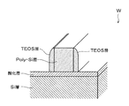
以下,本発明の好適な実施形態を説明する。先ず,本実施の形態にかかる処理方法によって処理される基板であるウェハの構造について説明する。図1は,エッチング処理前のウェハWの概略断面図であり,ウェハWの表面(デバイス形成面)の一部分を示している。ウェハWは,例えば略円盤形に形成された薄板状をなすシリコンウェハであり,その表面には,ウェハWの基材であるSi(シリコン)層,層間絶縁層として用いられる酸化層(二酸化シリコン:SiO2),ゲート電極として用いられるPoly−Si(多結晶シリコン)層,及び,絶縁体からなる側壁部(サイドウォール)として例えばTEOS(テトラエチルオルソシリケート:Si(OC2H5)4)層からなる構造が形成されている。Si層の表面(上面)は略平坦面となっており,酸化層は,Si層の表面を覆うように積層されている。また,この酸化層は,例えば拡散炉によって熱CVD反応により成膜される。Poly−Si層は,酸化層の表面上に形成されており,また,所定のパターン形状に沿ってエッチングされている。従って,酸化層は一部分がPoly−Si層によって覆われ,他の一部分は露出させられた状態になっている。TEOS層は,Poly−Si層の側面を覆うように形成されている。図示の例では,Poly−Si層は,略角柱状の断面形状を有し,図1において手前側から奥側に向かう方向に延設された細長い板状に形成されており,TEOS層は,Poly−Si層の左右両側面において,それぞれ手前側から奥側に向かう方向に沿って,また,Poly−Si層の下縁から上縁まで覆うように設けられている。そして,Poly−Si層とTEOS層の左右両側において,酸化層の表面が露出させられた状態になっている。 Hereinafter, preferred embodiments of the present invention will be described. First, the structure of a wafer that is a substrate processed by the processing method according to the present embodiment will be described. FIG. 1 is a schematic cross-sectional view of the wafer W before the etching process, and shows a part of the surface (device formation surface) of the wafer W. The wafer W is, for example, a silicon wafer having a thin plate shape formed in a substantially disc shape, and an Si (silicon) layer as a base material of the wafer W and an oxide layer (silicon dioxide) used as an interlayer insulating layer on the surface thereof. : SiO 2 ), a Poly-Si (polycrystalline silicon) layer used as a gate electrode, and a TEOS (tetraethyl orthosilicate: Si (OC 2 H 5 ) 4 ) layer as a side wall portion (side wall) made of an insulator The structure which consists of is formed. The surface (upper surface) of the Si layer is a substantially flat surface, and the oxide layer is laminated so as to cover the surface of the Si layer. The oxide layer is formed by a thermal CVD reaction using a diffusion furnace, for example. The Poly-Si layer is formed on the surface of the oxide layer, and is etched along a predetermined pattern shape. Therefore, a part of the oxide layer is covered with the Poly-Si layer and the other part is exposed. The TEOS layer is formed so as to cover the side surface of the Poly-Si layer. In the illustrated example, the Poly-Si layer has a substantially prismatic cross-sectional shape, and is formed in an elongated plate shape extending in a direction from the near side to the far side in FIG. On both the left and right side surfaces of the Poly-Si layer, the poly-Si layer is provided so as to cover from the near side to the far side and from the lower edge to the upper edge of the Poly-Si layer. And the surface of the oxide layer is exposed on both the left and right sides of the Poly-Si layer and the TEOS layer.
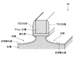
図2は,エッチング処理後のウェハWの状態を示している。ウェハWは,図1に示したようにSi層上に酸化層,Poly−Si層,TEOS層等が形成された後,例えばドライエッチングが施される。これにより,図2に示すように,ウェハWの表面では,露出させられていた酸化層,及び,その酸化層によって覆われていたSi層の一部が除去される。即ち,Poly−Si層とTEOS層の左右両側に,エッチングにより生じた凹部がそれぞれ形成される。凹部は,酸化層の表面の高さからSi層中まで陥没するように形成され,凹部の内面においては,Si層が露出した状態になる。Si層は酸化されやすいので,このように凹部において露出させられたSiの表面に大気中の酸素が付着すると,凹部の内面に自然酸化膜(二酸化シリコン:SiO2)が形成される。 FIG. 2 shows the state of the wafer W after the etching process. The wafer W is subjected to, for example, dry etching after an oxide layer, a Poly-Si layer, a TEOS layer, etc. are formed on the Si layer as shown in FIG. As a result, as shown in FIG. 2, the exposed oxide layer and a part of the Si layer covered with the oxide layer are removed from the surface of the wafer W. That is, the concave portions generated by etching are formed on both the left and right sides of the Poly-Si layer and the TEOS layer. The recess is formed so as to sink from the height of the surface of the oxide layer to the Si layer, and the Si layer is exposed on the inner surface of the recess. Since the Si layer is easily oxidized, when oxygen in the atmosphere adheres to the surface of Si exposed in this way, a natural oxide film (silicon dioxide: SiO 2 ) is formed on the inner surface of the recess.
次に,エッチング後のウェハWに対してCOR処理,PHT(Post Heat Treatment)処理,SiGe層成膜処理を行う処理システムについて説明する。なお,COR処理は,ハロゲン元素を含むガスと塩基性ガスを処理ガスとしてウェハに供給することで,ウェハ上に付着した自然酸化膜と処理ガスのガス分子とを化学反応させ,反応生成物を生成させるものである。ハロゲン元素を含むガスとは例えばフッ化水素ガスであり,塩基性ガスとは例えばアンモニアガスであり,この場合,主にフルオロケイ酸アンモニウムを含む反応生成物が生成される。PHT処理は,COR処理が施された後のウェハを加熱して,COR処理による反応生成物を気化させる処理である。 Next, a processing system that performs COR processing, PHT (Post Heat Treatment) processing, and SiGe layer deposition processing on the etched wafer W will be described. In the COR process, a gas containing a halogen element and a basic gas are supplied to the wafer as a process gas, so that a natural oxide film adhering to the wafer and a gas molecule of the process gas are chemically reacted to generate a reaction product. It is generated. The gas containing a halogen element is, for example, hydrogen fluoride gas, and the basic gas is, for example, ammonia gas. In this case, a reaction product mainly containing ammonium fluorosilicate is generated. The PHT process is a process for heating the wafer after the COR process and vaporizing a reaction product by the COR process.
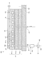
図3に示す処理システム1は,ウェハWを処理システム1に対して搬入出させる搬入出部2,略多角形状(例えば六角形状)に形成された共通搬送室3,ウェハWに対してCOR処理を行う本実施形態にかかる基板処理装置(真空処理装置)としてのCOR処理装置5,ウェハWに対してPHT処理を行う基板処理装置としてのPHT処理装置6,SiGe層の成膜処理を行う基板処理装置としての複数台,例えば2台のエピタキシャル成長装置7A,7B,処理システム1の各部に制御命令を与える制御コンピュータ8を備えている。
A
搬入出部2は,例えば略円盤形状をなすウェハWを搬送する第一のウェハ搬送機構11が内部に設けられた搬送室12を有している。ウェハ搬送機構11は,ウェハWを略水平に保持する2つの搬送アーム11a,11bを有している。搬送室12の側方には,ウェハWを複数枚並べて収容可能なキャリアCを載置する載置台13が,例えば3つ備えられている。また,ウェハWを回転させて偏心量を光学的に求めて位置合わせを行うオリエンタ14が設置されている。
The loading /
搬送室12と共通搬送室3は,真空引き可能な2つのロードロック室20A,20Bを介して互いに連結させられている。各ロードロック室20A,20Bと搬送室12との間,及び,各ロードロック室20A,20Bと共通搬送室3との間には,開閉可能なゲートバルブ21がそれぞれ備えられている。なお,これら2つのロードロック室20A,20Bは,いずれか一方(例えばロードロック室20A)が,ウェハWを搬送室12から搬出して共通搬送室3に搬入する際に用いられ,他方(例えばロードロック室20B)は,ウェハWを共通搬送室3から搬出して搬送室12に搬入する際に用いられるとしても良い。
The
かかる搬入出部2において,ウェハWは,搬送アーム11a,11bによって保持され,ウェハ搬送装置11の駆動により略水平面内で回転及び直進移動,また昇降させられることにより,所望の位置に搬送させられる。そして,載置台10上のキャリアC,オリエンタ14,ロードロック室20A,20Bに対してそれぞれ搬送アーム11a,11bが進退させられることにより,搬入出させられるようになっている。
In the loading /
共通搬送室3には,ウェハWを搬送する第二のウェハ搬送機構31が設けられている。ウェハ搬送機構31は,ウェハWを略水平に保持する2つの搬送アーム31a,31bを有している。
In the
共通搬送室3の外側には,COR処理装置5,PHT処理装置6,エピタキシャル成長装置7A,エピタキシャル成長装置7B,ロードロック室20B,ロードロック室20Aが,共通搬送室3の周囲を囲むように,例えば上方からみて時計回転方向においてこの順に並ぶように配置されている。共通搬送室3とCOR処理装置5内の処理室32との間,共通搬送室3とPHT処理装置6内の処理室33との間,共通搬送室3と各エピタキシャル成長装置7A,7B内の処理室34との間には,それぞれ開閉可能なゲートバルブ35が設けられている。
Outside the
かかる共通搬送室3において,ウェハWは,搬送アーム31a,31bによって保持され,ウェハ搬送機構31の駆動により略水平面内で回転及び直進移動,また昇降させられることにより,所望の位置に搬送させられる。そして,各ロードロック室20A,20B,COR処理装置5内の処理室32,PHT処理装置6内の処理室33,各エピタキシャル成長装置7A,7B内の処理室34に対して,それぞれ搬送アーム31a,31bが進退させられることにより,各処理室に対して搬入出させられるようになっている。
In the
図4に示すように,COR処理装置5は,筐体5aを備えており,筐体5aの内部は,ウェハWを収納する密閉構造の処理室(処理空間)32になっている。筐体5aの一側面には,ウェハWを処理室32内に搬入出させるための搬入出口36が設けられており,この搬入出口36に,前述したゲートバルブ35が設けられている。
As shown in FIG. 4, the
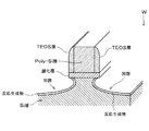
処理室32内には,ウェハWを略水平にした状態で載置させる載置台40が設けられている。図5及び図6に示すように,載置台40は,平面視において略円形をなすチャック本体41を備えており,チャック本体41の略平坦な上面41aが略水平になるように配置されている。かかる上面41aには,ウェハWの下面に当接させられる当接部材としての当接ピン42が,複数個,上方に向かって突出するように設けられている。図5に示す例では,当接ピン42は3個設けられており,上面41aの中央部を囲むように,上面41aの周縁部に設けられている。かかる構成において,ウェハWは,下面周縁部の3箇所を当接ピン42の上端部にそれぞれ載せた状態で,チャック本体41の上方において略水平に支持される。このように当接ピン42によって支持されたウェハWの下面とチャック本体41の上面41aとの間には,高さ方向において所定の幅Hを有する隙間Gが形成される。
In the
また,図6に示すように,チャック本体41は,筐体5aの底部に固定されている基部41bと,上面41aを有し当接ピン42が取り付けられている上層部41cとを備えており,基部41bと上層部41cとの間に,断熱材41dが設けられた構造になっている。
As shown in FIG. 6, the
また,COR処理装置5には,載置台40(上層部41c)の温度を所定の温度に調節することによりウェハWの温度を調節するための温度調節器46が設けられている。温度調節器46は,温調用の液体(例えば水など)が通過させられる管路47,ポンプ48,温調用の液体の温度を調節する液温調節部49を備えている。管路47は,例えば筐体5aの底部から載置台40の周縁部に導入されており,上層部41cの内部において,上層部41cの周縁部から所定の回転方向に沿って上層部41cの中心部に向かう渦巻状に配設されており,載置台40の中心部において,筐体5aの底部から外側に導出されている。管路47の上流端は,筐体5aの外部に設けられたポンプ48に接続されている。液温調節部49は,筐体5aの外部において管路47に介設されている。かかる構成において,温調用の液体は,ポンプ48の作動により,管路47内を流れ,液温調節部49において温調された後,載置台40の上層部41c内に供給され,載置台40の中心部において,筐体5aから導出される。こうして上層部41c内を液体が通過する間に,上層部41cと液体との間で熱交換が行われることにより,上層部41cの温度が調節されるように構成されている。なお,上層部41cと基部41bとの間には,断熱材41dが設けられているので,この断熱材41dにより,上層部41cの熱が筐体5aの外部に逃げることを防止できるようになっている。
Further, the
また,図4に示すように,COR処理装置5には,処理室32にガスを供給する供給機構50が設けられている。供給機構50は,処理室32にハロゲン元素を含む処理ガスとしてフッ化水素ガス(HF)を供給する供給路51,処理室32に塩基性ガスとしてアンモニアガス(NH3)を供給する供給路52,処理室32に不活性ガスとしてアルゴンガス(Ar)を供給する供給路53,処理室32に不活性ガスとして窒素ガス(N2)を供給する供給路54,及び,シャワーヘッド55を備えている。供給路51はフッ化水素ガスの供給源61に接続されている。また,供給路51には,供給路51の開閉動作及びフッ化水素ガスの供給流量の調節が可能な流量調整弁62が介設されている。供給路52はアンモニアガスの供給源63に接続されている。また,供給路52には,供給路52の開閉動作及びアンモニアガスの供給流量の調節が可能な流量調整弁64が介設されている。供給路53はアルゴンガスの供給源65に接続されている。また,供給路53には,供給路53の開閉動作及びアルゴンガスの供給流量の調節が可能な流量調整弁66が介設されている。供給路54は窒素ガスの供給源67に接続されている。また,供給路54には,供給路54の開閉動作及び窒素ガスの供給流量の調節が可能な流量調整弁68が介設されている。これら供給路51,52,53,54は,処理室32の天井部に設けられたシャワーヘッド55に接続されており,シャワーヘッド55から処理室32内に,フッ化水素ガス,アンモニアガス,アルゴンガス,窒素ガスが拡散されるように吐出される。
As shown in FIG. 4, the
さらに,COR処理装置5には,処理室32からガスを排気するための排気機構71が設けられている。排気機構71は,開閉弁72,強制排気を行うための排気ポンプ73が介設された排気路75を備えている。
Further, the
なお,図4及び図6に示すように,COR処理装置5のゲートバルブ35,ポンプ48,液温調節部49,流量調整弁62,64,66,68,開閉弁72,排気ポンプ73等の各部の動作は,制御コンピュータ8の制御命令によってそれぞれ制御されるようになっている。即ち,供給機構50によるフッ化水素ガス,アンモニアガス,アルゴンガス,窒素ガスの供給,排気機構71による排気,温度調節器46による温度調節などは,制御コンピュータ8によって制御される。
4 and 6, the
COR処理装置5の載置台40,筐体5a,シャワーヘッド55等の構成部品は,例えばアルマイト処理等の表面処理が施されたアルミニウム(Al)又はアルミニウム合金等の金属で構成される。ただし,このような構成部品の表面にアルマイト処理を施した場合,表面から硫酸アルミニウム(Al2(SO4)3)等の金属パーティクルが発生しやすくなり,ウェハWが汚染されるおそれがある。かかる金属パーティクルの発生を低減するためには,表面処理が施されていない無垢のアルミニウム,または,窒化アルミニウム(AIN)等を用いた構成にしても良い。また,例えば載置台40やシャワーヘッド55等の部品においては,アルミニウムの表面を石英(SiO2)等で被覆したものを用いても良い。この場合も,金属パーティクルの発生を効果的に低減できる。
Components such as the mounting table 40, the
図7に示すように,PHT処理装置6は,ウェハWを収納する密閉構造の処理室(処理空間)33を備えており,処理室33内には,ウェハWを略水平にして載置させる載置台80が設けられている。また,図示はしないが,ウェハWを処理室33内に搬入出させるための搬入出口が設けられており,この搬入出口に,前述したゲートバルブ35が設けられている。
As shown in FIG. 7, the PHT processing apparatus 6 includes a sealed processing chamber (processing space) 33 for storing the wafer W, and the wafer W is placed in the
PHT処理装置6の載置台80等の構成部品は,例えばアルマイト処理が施されたアルミニウム(Al),又は,表面処理が施されていない無垢のアルミニウム等によって構成しても良い。ただし,表面から発生した硫酸アルミニウム等の金属パーティクルが熱泳動によりウェハWの下面に転写することがある。一般に,載置台80の温度が高温(例えば160℃以上)に昇温させられるほど,処理室33におけるPHT処理の反応は促進されやすくなるが,熱泳動によるパーティクルの転写も生じやすくなる。そのため,載置台80の温度は高温にさせすぎず,例えば150℃以下程度,望ましくは,100℃〜135℃程度にすると良い。そうすれば,反応を良好に促進させながら,ウェハWへのパーティクルの付着も低減することができる。
The components such as the mounting table 80 of the PHT processing apparatus 6 may be made of, for example, aluminum (Al) that has been subjected to alumite treatment, or solid aluminum that has not been subjected to surface treatment. However, metal particles such as aluminum sulfate generated from the surface may be transferred to the lower surface of the wafer W by thermophoresis. In general, as the temperature of the mounting table 80 is raised to a higher temperature (for example, 160 ° C. or more), the reaction of the PHT process in the
さらに,PHT処理装置6には,処理室33に例えば窒素ガス(N2)などの不活性ガスを加熱して供給する供給路81を備えた供給機構82,処理室33を排気する排気路83を備えた排気機構84が備えられている。供給路81は窒素ガスの供給源85に接続されている。また,供給路81には,供給路81の開閉動作及び窒素ガスの供給流量の調節が可能な流量調整弁86が介設されている。排気路83には,開閉弁87,強制排気を行うための排気ポンプ88が介設されている。
Further, the PHT processing apparatus 6 includes a
なお,PHT処理装置6のゲートバルブ35,流量調整弁86,排気ポンプ88等の各部の動作は,制御コンピュータ8の制御命令によってそれぞれ制御されるようになっている。
The operation of each part such as the
処理システム1の各機能要素は,処理システム1全体の動作を自動制御する制御コンピュータ8に,信号ラインを介して接続されている。ここで,機能要素とは,例えば前述したCOR処理装置5のゲートバルブ35,ポンプ48,液温調節部49,流量調整弁62,64,66,68,開閉弁72,排気ポンプ73,PHT処理装置6のゲートバルブ35,流量調整弁86,排気ポンプ88等の,所定のプロセス条件を実現するために動作する総ての要素を意味している。制御コンピュータ8は,典型的には,実行するソフトウェアに依存して任意の機能を実現することができる汎用コンピュータである。
Each functional element of the
図3に示すように,制御コンピュータ8は,CPU(中央演算装置)を備えた演算部8aと,演算部8aに接続された入出力部8bと,入出力部8bに挿着され制御ソフトウェアを格納した記録媒体8cと,を有する。この記録媒体8cには,制御コンピュータ8によって実行されることにより処理システム1に後述する所定の基板処理方法を行わせる制御ソフトウェア(プログラム)が記録されている。制御コンピュータ8は,該制御ソフトウェアを実行することにより,処理システム1の各機能要素を,所定のプロセスレシピにより定義された様々なプロセス条件(例えば,処理室32の圧力等)が実現されるように制御する。例えば,COR処理装置5に対しては,後に詳細に説明するように,処理室32を所定の圧力P2にした状態でウェハWの温度を調節する制御(ステップS2を実現する制御),処理室32を圧力P3の処理雰囲気にする制御(ステップS4を実現する制御)など,ステップS1〜S5が順番に行われるように制御命令を与える。
As shown in FIG. 3, the
記録媒体8cは,制御コンピュータ8に固定的に設けられるもの,あるいは,制御コンピュータ8に設けられた図示しない読み取り装置に着脱自在に装着されて該読み取り装置により読み取り可能なものであっても良い。最も典型的な実施形態においては,記録媒体8cは,処理システム1のメーカーのサービスマンによって制御ソフトウェアがインストールされたハードディスクドライブである。他の実施形態においては,記録媒体8cは,制御ソフトウェアが書き込まれたCD−ROM又はDVD−ROMのような,リムーバブルディスクである。このようなリムーバブルディスクは,制御コンピュータ8に設けられた図示しない光学的読取装置により読み取られる。また,記録媒体8cは,RAM(random access memory)又はROM(read only memory)のいずれの形式のものであっても良い。さらに,記録媒体8cは,カセット式のROMのようなものであっても良い。要するに,コンピュータの技術分野において知られている任意のものを記録媒体8cとして用いることが可能である。なお,複数の処理システム1が配置される工場においては,各処理システム1の制御コンピュータ8を統括的に制御する管理コンピュータに,制御ソフトウェアが格納されていても良い。この場合,各処理システム1は,通信回線を介して管理コンピュータにより操作され,所定のプロセスを実行する。
The
次に,以上のように構成された処理システム1が使用されるウェハWの処理方法について説明する。先ず,図1に示したようにSi層,酸化層,Poly−Si層,TEOS層を有するウェハWが,ドライエッチング装置等によりエッチング処理され,図2に示したように,Siが露出した凹部が形成される。かかるドライエッチング処理後のウェハWが,キャリアC内に収納され,処理システム1に搬送される。
Next, a processing method of the wafer W in which the
処理システム1においては,図3に示すように,複数枚のウェハWが収納されたキャリアCが載置台13上に載置され,ウェハ搬送機構11によってキャリアCから一枚のウェハWが取り出され,ロードロック室20Aに搬入される。ロードロック室20AにウェハWが搬入されると,ロードロック室20Aが密閉され,減圧される。その後,ロードロック室20Aと大気圧に対して減圧された共通搬送室3とが連通させられる。そして,ウェハ搬送機構31によって,ウェハWがロードロック室20Aから搬出され,共通搬送室3に搬入される。
In the
共通搬送室3に搬入されたウェハWは,先ずCOR処理装置5の処理室32に搬入される。ウェハWは,表面(デバイス形成面)を上面とした状態で,ウェハ搬送機構31から載置台40に受け渡される。ウェハWが搬入されると搬入出口36が閉じられ,COR処理を含む一連の工程が開始される。このCOR処理装置5において行われる工程については,後に詳細に説明する。COR処理によって,ウェハWの凹部の自然酸化膜は反応生成物に変質させられる(図8参照)。
The wafer W loaded into the
COR処理装置5における工程が終了すると,搬入出口36が開かれ,ウェハWはウェハ搬送機構31によって処理室32から搬出され,PHT処理装置6の処理室33に搬入される。
When the process in the
PHT処理装置6において,ウェハWは表面を上面とした状態で処理室33内に載置される。ウェハWが搬入されると処理室33が密閉され,PHT処理が開始される。PHT処理では,処理室33内が排気路83によって排気されながら,供給路81によって高温の加熱ガスが処理室33内に供給され,加熱ガスにより処理室33内が昇温される。これにより,上記COR処理によって生じた反応生成物が加熱されて気化し,凹部の内面から除去され,Si層の表面が露出させられる(図9参照)。処理室33内の温度及び圧力は,反応生成物が気化する条件に制御され,例えば約100℃以上の温度に加熱される。このように,COR処理の後,PHT処理を行うことにより,ウェハWをドライ洗浄でき,自然酸化膜をドライエッチングするようにして,Si層から除去することができる。
In the PHT processing apparatus 6, the wafer W is placed in the
PHT処理が終了すると,加熱ガスの供給が停止され,PHT処理装置6の搬入出口が開かれる。その後,ウェハWはウェハ搬送機構31によって処理室33から搬出され,エピタキシャル成長装置7A又は7Bの処理室34に搬入される。
When the PHT process is completed, the supply of the heated gas is stopped and the loading / unloading port of the PHT processing device 6 is opened. Thereafter, the wafer W is unloaded from the
処理室34にウェハWが搬入されると,処理室34が密閉され,SiGeの成膜処理が開始される。成膜処理においては,処理室34内に供給される反応ガスとウェハWの凹部において露出したSi層とが化学反応することにより,凹部にSiGeがエピタキシャル成長する(図10参照)。ここで,前述したCOR処理とPHT処理により,凹部において露出させられているSi層の表面からは,自然酸化膜が除去されているので,SiGeはSi層の表面をベースとして,好適に成長させられる。
When the wafer W is loaded into the
このようにして,両側の凹部にSiGe層がそれぞれ形成されると,Si層では,SiGe層によって挟まれた部分が両側から圧縮応力を受ける。即ち,Poly−Si層及び酸化層の下方において,SiGe層によって挟まれた部分に,圧縮歪を有する歪Si層が形成される。 In this way, when the SiGe layers are formed in the concave portions on both sides, in the Si layer, the portion sandwiched between the SiGe layers receives compressive stress from both sides. That is, a strained Si layer having a compressive strain is formed in a portion sandwiched between the SiGe layers below the Poly-Si layer and the oxide layer.
こうしてSiGe層が形成され,成膜処理が終了すると,ウェハWはウェハ搬送機構31によって処理室34から搬出され,ロードロック室20Bに搬入される。ロードロック室20BにウェハWが搬入されると,ロードロック室20Bが密閉された後,ロードロック室20Bと搬送室12とが連通させられる。そして,ウェハ搬送機構11によって,ウェハWがロードロック室20Bから搬出され,載置台13上のキャリアCに戻される。以上のようにして,処理システム1における一連の工程が終了する。
When the SiGe layer is thus formed and the film forming process is completed, the wafer W is unloaded from the
次に,COR処理装置5にて行われる工程について詳細に説明する。処理室32への搬入時,ウェハ搬送機構31から載置台40に受け渡されたウェハWは,複数の当接ピン42にウェハWの下面周縁部を当接させた状態で,略水平に載置される。このように当接ピン42によって下面が支持された状態では,ウェハWは載置台40の上面41aに対して上方に離隔させられ,ウェハWの下面と上面41aとの間に隙間Gが形成される。なお,ウェハWを処理室32へ搬入する際は,処理室32の圧力は,大気圧POより減圧された真空状態に近い圧力P1になっている。
Next, the process performed in the
ウェハWが処理室32に搬入され載置台40に受け渡されたら,処理室32を密閉した後,各供給路52,53,54から処理室32にそれぞれアンモニアガス,アルゴンガス,窒素ガスを供給する。これにより,処理室32内は,ウェハW搬入時の最初の圧力P1から所定の圧力P2(例えば約2Torr(約2.67×10²Pa)程度,P1<P2<PO)に加圧される(図11及び図12においてステップS1)。
When the wafer W is loaded into the
処理室32内が所定の圧力P2になったら,アンモニアガス,窒素ガス,アルゴンガスの供給を停止させ,次に,温度調節器46によってウェハWの温度を所定の目標値(例えば約25℃程度)に調節する(ステップS2)。ウェハWを温調する際には,管路47に液体が通過させられ,載置台40の上層部41cの温度が所定の温度に調節される。ここで,ウェハWの下面は上面41aに対して近接させられているものの,隙間Gを空けて離隔させられているが,処理室32には予めアンモニアガス,アルゴンガス,窒素ガスが導入されており,これらの混合ガスが隙間Gに侵入した状態になっている。従って,ウェハWが上面41aに直接的に接触していなくても,隙間G内の混合ガスを介して,ウェハWと上面41aとの間で熱交換が行われるので,ウェハWの温度を上面41aの温度に効率的に近づけることができる。従って,処理室32を圧力P2にした状態で,上層部41cの温度を調節することにより,上層部41cの熱(冷熱)を混合ガスを介してウェハWに伝熱させ,ウェハWの温度を確実に調節することができる。
When the inside of the
ウェハWの温調が終了したら,次に,処理室32内を強制排気して,処理室32を圧力P2より低い圧力P3(例えば約0.1Torr(約13.3Pa)以下程度,P1<P3<P2)に減圧させる(ステップS3)。処理室32の圧力が安定し,圧力P3になったら,供給路51から処理室32にフッ化水素ガスを供給する。ここで処理室32には,予めアンモニアガスが供給されているので,フッ化水素ガスを供給することにより,処理室32の雰囲気はフッ化水素ガスとアンモニアガスとを含む処理雰囲気にされ,ウェハWに対してCOR処理(ステップS4)が開始される。かかる低圧状態の処理雰囲気によって,ウェハWの表面に存在する自然酸化膜が,フッ化水素ガスの分子及びアンモニアガスの分子と化学反応して,反応生成物に変質させられる。COR処理中は,処理室32の雰囲気が一定の圧力P3に維持されるようにする。
When the temperature control of the wafer W is completed, the inside of the
なお,このようにフッ化水素ガスを供給する前に,処理室32の圧力を減圧して圧力P3に安定させるようにすると,処理雰囲気の圧力を安定させやすく,また,処理雰囲気中のフッ化水素ガスやアンモニアガスの濃度の均一性を良好にすることができる。従って,ウェハWの処理むらを防止できる。また,フッ化水素ガスは液化しやすい,筐体5aの内壁に付着しやすいといった性質があるが,COR処理の直前に供給することにより,そのような問題が発生することを抑制できる。
If the pressure in the
COR処理が終了したら,再び処理室32を強制排気して,圧力P1に減圧する(ステップS5)。これにより,フッ化水素ガスやアンモニアガスが処理室32から排出される。その後,搬入出口36を開口させて,ウェハWを搬出させ,次の未処理のウェハWを処理室32に搬入させる。
When the COR processing is completed, the
かかるCOR処理装置5によれば,ウェハWの下面と載置台40の上面41aとの間に隙間Gが形成される構成としたことにより,載置台40からウェハWにパーティクルが転写することを防止できる。また,ウェハWの下面が載置台40の上面やパーティクルと擦れ合うことによるウェハWの損傷を防止できる。ウェハWの温度を調節する際は,処理室32内を所定の圧力P2に加圧することにより,ウェハWの下面と上面41aとの間の隙間Gに混合ガスを供給して,この混合ガスを媒体として,ウェハWと載置台40との間で熱を効率的に伝達させることができる。従って,ウェハWの温度を効率的に調節できる。
According to the
以上,本発明の好適な実施形態について説明したが,本発明はかかる例に限定されない。当業者であれば,特許請求の範囲に記載された技術的思想の範疇内において,各種の変更例または修正例に想到しうることは明らかであり,それらについても当然に本発明の技術的範囲に属するものと了解される。 The preferred embodiments of the present invention have been described above, but the present invention is not limited to such examples. It is obvious for those skilled in the art that various changes and modifications can be conceived within the scope of the technical idea described in the claims. It is understood that it belongs to.
以上の実施形態では,低圧状態で基板を処理する基板処理装置及び基板処理方法として,COR処理装置5及びCOR処理装置5を用いた処理方法を例示したが,本発明は,かかる装置及び方法に限定されず,他の基板処理装置及び基板処理方法,例えば,基板に対して例えばエッチング処理,CVD処理等を行う基板処理装置及び基板処理方法に適用することもできる。また,基板は半導体ウェハに限定されず,例えばLCD基板用ガラス,CD基板,プリント基板,セラミック基板などであっても良い。
In the above embodiment, the
本実施形態では,処理室32に供給される不活性ガスとして,アルゴンガス及び窒素ガスを例示したが,かかるものには限定されず,例えばアルゴンガスのみであっても良い。また,かかる不活性ガスは,その他の不活性ガス,例えば,ヘリウムガス(He),キセノンガス(Xe)のいずれかであっても良く,または,アルゴンガス,窒素ガス,ヘリウムガス,キセノンガスのうち2種類以上のガスを混合したものであっても良い。
In the present embodiment, argon gas and nitrogen gas are exemplified as the inert gas supplied to the
また,以上の実施形態では,処理室32に供給路52,53,54からガス供給を行うことにより,ウェハWと載置台40との隙間Gに対して,ガスを周囲から侵入させるようにして供給する構成としたが,隙間Gにガスを直接供給する供給口を設けても良い。例えば,載置台40の上面41aに,ヘリウム(He)又は窒素ガスなどの不活性ガスを吐出する供給口を設け,この供給口から載置台40に載置されたウェハWの下面に対して不活性ガスを供給できる構成としても良い。
In the above embodiment, gas is supplied from the surroundings to the gap G between the wafer W and the mounting table 40 by supplying gas from the
温度調節器46は,載置台40内に温調用の液体を流すことで温度調節を行う構成としたが,かかる構成には限定されず,例えば抵抗熱によって載置台40を加熱する電気ヒータ,又は,輻射熱によって載置台40を加熱するハロゲンランプヒータ等を備えた構成であっても良い。この場合も,電気ヒータやハロゲンランプヒータによって載置台40を加熱することにより,ウェハWを加熱できる。
The
本発明者らは,COR処理装置5における処理工程の各種条件について検討した。ステップS2におけるウェハWの温度の目標値は,例えば約10℃以上,60℃以下程度としても良い。ステップS2でウェハの温調を行う処理時間は,約15秒間以上,約300秒間以下としても良い。なお,温調の処理時間は長いほど,ウェハの温度を目標値に近づけることはできるが,処理システム1全体のスループットや生産性を考慮すると短いほうが望ましく,例えば約30秒以下程度にすると良い。処理室32の圧力P2は,約0.5Torr(約66.7Pa)以上,約100Torr(13.3×10³Pa)以下の値としても良い。なお,圧力P2は高いほどウェハを効率的に温調できるが,COR処理装置5の構造上の制約等を考慮すると,例えば約4Torr(約5.33×10²Pa)以下程度にすることが望ましいであろう。また,ステップS1〜S4において,各種ガスの供給を行う際,フッ化水素ガスの供給流量は約500sccm(約8.45×10⁻¹m3/s)以下,アンモニアガスの供給流量は約500sccm以下,アルゴンガスの供給流量は約2000sccm(約3.38m3/s)以下,窒素ガスの供給流量は約2000sccm以下としても良い。
The present inventors examined various conditions of the processing steps in the
また,本発明者らは,ステップS2でのウェハの温度調節における圧力依存性を調べた。図13は,ステップS2においてウェハを温調した処理時間を一定値(30秒間)としたときの,処理室32の圧力P2とウェハの温度との関係を示している。載置台40の上面41aの温度は25℃とし,温調前のウェハの温度は35℃とした。図13に示すように,圧力P2が0.9Torr(約1.20×10²Pa),2Torr,4Torr(約5.33×10²Pa)のとき,ウェハの温度はそれぞれ約29.48℃,約27.91℃,約27.32℃になるという結果が得られた。従って,圧力P2が高いほど,ウェハを効率的に温調できることが実証された。
In addition, the present inventors examined the pressure dependence in the temperature control of the wafer in step S2. FIG. 13 shows the relationship between the pressure P2 in the
また,本発明者らは,ステップS2でのウェハの温度調節における時間依存性を調べた。図14は,ステップS2において圧力P2を一定値(2Torr)としたときの,ウェハを温調した処理時間とウェハの温度との関係を示している。載置台40の上面41aの温度は25℃とし,温調前のウェハの温度は35℃とした。図14に示すように,処理時間が15秒,30秒,60秒のとき,ウェハの温度はそれぞれ約29.13℃,約27.91℃,約26.90℃に冷却されるという結果が得られた。従って,処理時間が長いほど,ウェハの温度が目標値(25℃)に近づくことが実証された。
In addition, the present inventors investigated the time dependency in wafer temperature control in step S2. FIG. 14 shows a relationship between the wafer processing temperature and the wafer temperature when the pressure P2 is set to a constant value (2 Torr) in step S2. The temperature of the
本発明は,低圧状態で基板の処理を行う基板処理装置,基板処理方法,及び,かかる基板処理装置に備えられる記録媒体に適用できる。 The present invention can be applied to a substrate processing apparatus, a substrate processing method, and a recording medium provided in the substrate processing apparatus for processing a substrate in a low pressure state.
W ウェハ
1 処理システム
5 COR処理装置
6 PHT処理装置
8 制御コンピュータ
8a 演算部
8c 記録媒体
32 処理室
33 処理室
40 載置台
41 チャック本体
41a 上面
42 当接ピン
46 温度調節器
47 管路
50 供給機構
51 フッ化水素ガスの供給路
52 アンモニアガスの供給路
53 アルゴンガスの供給路
54 窒素ガスの供給路
71 排気機構
75 排気路
Claims (13)
基板を収納する処理室,前記処理室にガスを供給する供給機構,及び,前記処理室を排気する排気機構を備え,
前記処理室に,基板を載置させる載置台を備え,
前記載置台の上面に,基板の下面に当接させられる当接部材を備え,
前記載置台は,基板の温度を調節する際および基板に所定の処理が施される際の両方において、前記当接部材によって基板の下面を支持し,該基板の下面と前記載置台の上面との間に隙間を形成した状態で,前記基板を載置させる構成とし,
前記載置台の温度を調節することにより前記当接部材に支持された基板の温度を調節する温度調節器を備え,
前記供給機構によるガスの供給,前記排気機構による排気,及び,前記温度調節器を制御する制御コンピュータを備え,
前記制御コンピュータは,前記処理室を所定の圧力にした状態で,前記載置台に載置された基板の温度を調節する制御と,前記処理室を前記所定の圧力より低い圧力,かつ,前記基板に前記所定の処理が施される処理雰囲気にする制御と,を行い、
前記処理雰囲気は,フッ化水素ガス及びアンモニアガスを含み,前記基板の表面に存在する二酸化シリコンを,加熱により気化させることが可能な反応生成物に変質させるものであることを特徴とする,基板処理装置。 An apparatus for processing a substrate,
A processing chamber for storing the substrate, a supply mechanism for supplying gas to the processing chamber, and an exhaust mechanism for exhausting the processing chamber;
The processing chamber includes a mounting table on which a substrate is mounted,
Provided on the top surface of the mounting table is a contact member that can contact the bottom surface of the substrate,
The mounting table supports the lower surface of the substrate by the contact member both when the temperature of the substrate is adjusted and when the substrate is subjected to a predetermined treatment, and the lower surface of the substrate, the upper surface of the mounting table, The substrate is placed in a state where a gap is formed between
A temperature controller for adjusting the temperature of the substrate supported by the contact member by adjusting the temperature of the mounting table;
A control computer for controlling the temperature controller by supplying gas by the supply mechanism, exhausting by the exhaust mechanism, and the temperature controller;
The control computer controls the temperature of the substrate placed on the mounting table in a state where the processing chamber is set to a predetermined pressure, and sets the processing chamber to a pressure lower than the predetermined pressure and the substrate. said predetermined process have line control and a to a processing atmosphere to be applied to,
The processing atmosphere contains hydrogen fluoride gas and ammonia gas, and changes the silicon dioxide present on the surface of the substrate into a reaction product that can be vaporized by heating. Processing equipment.
前記アンモニアガスが供給された処理室にフッ化水素ガスを供給させることにより,前記処理室を前記処理雰囲気にする制御を行うことを特徴とする,請求項1に記載の基板処理装置。 The substrate processing apparatus according to claim 1, wherein the processing chamber is controlled to be the processing atmosphere by supplying hydrogen fluoride gas to the processing chamber to which the ammonia gas is supplied.
基板を処理室に搬入し,
載置台の上面に設けられた当接部材に基板の下面を当接させ,前記基板の下面と前記載置台の上面との間に隙間を形成した状態で,前記当接部材に基板を支持させ,
前記処理室を所定の圧力にした状態で,前記載置台の温度を調節することにより,前記基板の温度を調節し,
その後,前記処理室を前記所定の圧力より低い圧力の処理雰囲気にして,前記基板に所定の処理を施し、
前記処理雰囲気は,フッ化水素ガス及びアンモニアガスを含み,
前記所定の処理は,前記基板の表面に存在する二酸化シリコンを前記処理雰囲気と反応させることにより反応生成物に変質させる処理であって,
前記所定の処理を施した後,前記反応生成物を加熱により気化させる処理を行うことを特徴とする,基板処理方法。 A method of processing a substrate, comprising:
Bring the substrate into the processing chamber,
The lower surface of the substrate is brought into contact with an abutting member provided on the upper surface of the mounting table, and the substrate is supported by the abutting member in a state where a gap is formed between the lower surface of the substrate and the upper surface of the mounting table. ,
Adjusting the temperature of the substrate by adjusting the temperature of the mounting table with the processing chamber at a predetermined pressure,
Then, the processing chamber is set to a processing atmosphere at a pressure lower than the predetermined pressure, and the substrate is subjected to a predetermined processing,
The treatment atmosphere includes hydrogen fluoride gas and ammonia gas,
The predetermined treatment is a treatment for transforming silicon dioxide present on the surface of the substrate into a reaction product by reacting with the treatment atmosphere,
A substrate processing method , wherein after the predetermined treatment is performed, the reaction product is vaporized by heating .
その後,前記アンモニアガスが供給された処理室にフッ化水素ガスを供給することにより,前記処理室を前記処理雰囲気にすることを特徴とする,請求項7に記載の基板処理方法。 The substrate processing method according to claim 7, wherein after that, the processing chamber is set to the processing atmosphere by supplying hydrogen fluoride gas to the processing chamber to which the ammonia gas is supplied.
前記プログラムは,前記制御コンピュータによって実行されることにより,前記基板処理装置に,請求項7〜12のいずれかに記載の基板処理方法を行わせるものであることを特徴とする,記録媒体。 13. The recording medium according to claim 7, wherein the program is executed by the control computer to cause the substrate processing apparatus to perform the substrate processing method according to any one of claims 7 to 12.
Priority Applications (3)
| Application Number | Priority Date | Filing Date | Title |
|---|---|---|---|
| JP2005323329A JP4976002B2 (en) | 2005-11-08 | 2005-11-08 | Substrate processing apparatus, substrate processing method, and recording medium |
| PCT/JP2006/322155 WO2007055190A1 (en) | 2005-11-08 | 2006-11-07 | Substrate processing apparatus, substrate processing method and recording medium |
| TW095141331A TW200739701A (en) | 2005-11-08 | 2006-11-08 | Apparatus and method for processing substrate and recording medium |
Applications Claiming Priority (1)
| Application Number | Priority Date | Filing Date | Title |
|---|---|---|---|
| JP2005323329A JP4976002B2 (en) | 2005-11-08 | 2005-11-08 | Substrate processing apparatus, substrate processing method, and recording medium |
Related Child Applications (1)
| Application Number | Title | Priority Date | Filing Date |
|---|---|---|---|
| JP2012054102A Division JP2012124529A (en) | 2012-03-12 | 2012-03-12 | Substrate processing apparatus, substrate processing method, and recording medium |
Publications (2)
| Publication Number | Publication Date |
|---|---|
| JP2007134379A JP2007134379A (en) | 2007-05-31 |
| JP4976002B2 true JP4976002B2 (en) | 2012-07-18 |
Family
ID=38023193
Family Applications (1)
| Application Number | Title | Priority Date | Filing Date |
|---|---|---|---|
| JP2005323329A Active JP4976002B2 (en) | 2005-11-08 | 2005-11-08 | Substrate processing apparatus, substrate processing method, and recording medium |
Country Status (3)
| Country | Link |
|---|---|
| JP (1) | JP4976002B2 (en) |
| TW (1) | TW200739701A (en) |
| WO (1) | WO2007055190A1 (en) |
Families Citing this family (4)
| Publication number | Priority date | Publication date | Assignee | Title |
|---|---|---|---|---|
| JP5478280B2 (en) * | 2010-01-27 | 2014-04-23 | 東京エレクトロン株式会社 | Substrate heating apparatus, substrate heating method, and substrate processing system |
| JP6400361B2 (en) | 2014-07-16 | 2018-10-03 | 東京エレクトロン株式会社 | Substrate cleaning method, substrate processing method, substrate processing system, and semiconductor device manufacturing method |
| JP6692202B2 (en) * | 2016-04-08 | 2020-05-13 | 東京エレクトロン株式会社 | Substrate processing method and substrate processing apparatus |
| JP7145019B2 (en) * | 2018-09-19 | 2022-09-30 | 株式会社Screenホールディングス | Recipe conversion method, recipe conversion program, recipe conversion apparatus, and substrate processing system |
Family Cites Families (3)
| Publication number | Priority date | Publication date | Assignee | Title |
|---|---|---|---|---|
| JP4124543B2 (en) * | 1998-11-11 | 2008-07-23 | 東京エレクトロン株式会社 | Surface treatment method and apparatus |
| JP2004128019A (en) * | 2002-09-30 | 2004-04-22 | Applied Materials Inc | Method and apparatus for plasma processing |
| JP4039385B2 (en) * | 2003-04-22 | 2008-01-30 | 東京エレクトロン株式会社 | Removal method of chemical oxide film |
-
2005
- 2005-11-08 JP JP2005323329A patent/JP4976002B2/en active Active
-
2006
- 2006-11-07 WO PCT/JP2006/322155 patent/WO2007055190A1/en active Application Filing
- 2006-11-08 TW TW095141331A patent/TW200739701A/en unknown
Also Published As
| Publication number | Publication date |
|---|---|
| TWI313893B (en) | 2009-08-21 |
| TW200739701A (en) | 2007-10-16 |
| JP2007134379A (en) | 2007-05-31 |
| WO2007055190A1 (en) | 2007-05-18 |
Similar Documents
| Publication | Publication Date | Title |
|---|---|---|
| JP4949091B2 (en) | Substrate processing apparatus, substrate processing method, and recording medium | |
| JP5352103B2 (en) | Heat treatment apparatus and treatment system | |
| TWI686843B (en) | Substrate processing method and substrate processing device | |
| JP4890025B2 (en) | Etching method and recording medium | |
| KR100982859B1 (en) | Substrate processing apparatus, substrate processing method and recording medium | |
| KR101100466B1 (en) | Substrate processing apparatus | |
| JP5809144B2 (en) | Substrate processing method and substrate processing apparatus | |
| JP2008235309A (en) | Substrate treating device, substrate treatment method, and recording medium | |
| TWI727023B (en) | Substrate processing method and substrate processing device | |
| JP5881612B2 (en) | Semiconductor device manufacturing method and manufacturing apparatus | |
| TWI692806B (en) | Substrate processing method and substrate processing device | |
| JPWO2007049510A1 (en) | Processing method and recording medium | |
| JP4913485B2 (en) | Etching method and recording medium | |
| KR20180116327A (en) | Substrate processing method | |
| JP4976002B2 (en) | Substrate processing apparatus, substrate processing method, and recording medium | |
| WO2014208365A2 (en) | Etching method, and recording medium | |
| JP2012124529A (en) | Substrate processing apparatus, substrate processing method, and recording medium | |
| WO2017026001A1 (en) | Method for manufacturing semiconductor device, substrate processing apparatus, and recording medium | |
| KR20090103782A (en) | Heat treatment apparatus and treatment system |
Legal Events
| Date | Code | Title | Description |
|---|---|---|---|
| A621 | Written request for application examination |
Free format text: JAPANESE INTERMEDIATE CODE: A621 Effective date: 20081027 |
|
| A131 | Notification of reasons for refusal |
Free format text: JAPANESE INTERMEDIATE CODE: A131 Effective date: 20110712 |
|
| A521 | Request for written amendment filed |
Free format text: JAPANESE INTERMEDIATE CODE: A523 Effective date: 20110912 |
|
| A131 | Notification of reasons for refusal |
Free format text: JAPANESE INTERMEDIATE CODE: A131 Effective date: 20120110 |
|
| A521 | Request for written amendment filed |
Free format text: JAPANESE INTERMEDIATE CODE: A523 Effective date: 20120312 |
|
| TRDD | Decision of grant or rejection written | ||
| A01 | Written decision to grant a patent or to grant a registration (utility model) |
Free format text: JAPANESE INTERMEDIATE CODE: A01 Effective date: 20120410 |
|
| A01 | Written decision to grant a patent or to grant a registration (utility model) |
Free format text: JAPANESE INTERMEDIATE CODE: A01 |
|
| A61 | First payment of annual fees (during grant procedure) |
Free format text: JAPANESE INTERMEDIATE CODE: A61 Effective date: 20120412 |
|
| R150 | Certificate of patent or registration of utility model |
Free format text: JAPANESE INTERMEDIATE CODE: R150 Ref document number: 4976002 Country of ref document: JP Free format text: JAPANESE INTERMEDIATE CODE: R150 |
|
| FPAY | Renewal fee payment (event date is renewal date of database) |
Free format text: PAYMENT UNTIL: 20150420 Year of fee payment: 3 |
|
| R250 | Receipt of annual fees |
Free format text: JAPANESE INTERMEDIATE CODE: R250 |
|
| R250 | Receipt of annual fees |
Free format text: JAPANESE INTERMEDIATE CODE: R250 |
|
| R250 | Receipt of annual fees |
Free format text: JAPANESE INTERMEDIATE CODE: R250 |
|
| R250 | Receipt of annual fees |
Free format text: JAPANESE INTERMEDIATE CODE: R250 |
|
| R250 | Receipt of annual fees |
Free format text: JAPANESE INTERMEDIATE CODE: R250 |
|
| R250 | Receipt of annual fees |
Free format text: JAPANESE INTERMEDIATE CODE: R250 |