JP4024867B2 - Efficient parallel stage power amplifier - Google Patents
Efficient parallel stage power amplifier Download PDFInfo
- Publication number
- JP4024867B2 JP4024867B2 JP52679198A JP52679198A JP4024867B2 JP 4024867 B2 JP4024867 B2 JP 4024867B2 JP 52679198 A JP52679198 A JP 52679198A JP 52679198 A JP52679198 A JP 52679198A JP 4024867 B2 JP4024867 B2 JP 4024867B2
- Authority
- JP
- Japan
- Prior art keywords
- amplifier
- signal
- input
- stage
- output
- Prior art date
- Legal status (The legal status is an assumption and is not a legal conclusion. Google has not performed a legal analysis and makes no representation as to the accuracy of the status listed.)
- Expired - Lifetime
Links
Images


Classifications
-
- H—ELECTRICITY
- H03—ELECTRONIC CIRCUITRY
- H03F—AMPLIFIERS
- H03F3/00—Amplifiers with only discharge tubes or only semiconductor devices as amplifying elements
- H03F3/20—Power amplifiers, e.g. Class B amplifiers, Class C amplifiers
- H03F3/21—Power amplifiers, e.g. Class B amplifiers, Class C amplifiers with semiconductor devices only
- H03F3/211—Power amplifiers, e.g. Class B amplifiers, Class C amplifiers with semiconductor devices only using a combination of several amplifiers
-
- H—ELECTRICITY
- H03—ELECTRONIC CIRCUITRY
- H03F—AMPLIFIERS
- H03F1/00—Details of amplifiers with only discharge tubes, only semiconductor devices or only unspecified devices as amplifying elements
- H03F1/02—Modifications of amplifiers to raise the efficiency, e.g. gliding Class A stages, use of an auxiliary oscillation
- H03F1/0205—Modifications of amplifiers to raise the efficiency, e.g. gliding Class A stages, use of an auxiliary oscillation in transistor amplifiers
- H03F1/0277—Selecting one or more amplifiers from a plurality of amplifiers
-
- H—ELECTRICITY
- H03—ELECTRONIC CIRCUITRY
- H03F—AMPLIFIERS
- H03F1/00—Details of amplifiers with only discharge tubes, only semiconductor devices or only unspecified devices as amplifying elements
- H03F1/02—Modifications of amplifiers to raise the efficiency, e.g. gliding Class A stages, use of an auxiliary oscillation
- H03F1/0205—Modifications of amplifiers to raise the efficiency, e.g. gliding Class A stages, use of an auxiliary oscillation in transistor amplifiers
- H03F1/0288—Modifications of amplifiers to raise the efficiency, e.g. gliding Class A stages, use of an auxiliary oscillation in transistor amplifiers using a main and one or several auxiliary peaking amplifiers whereby the load is connected to the main amplifier using an impedance inverter, e.g. Doherty amplifiers
-
- H—ELECTRICITY
- H03—ELECTRONIC CIRCUITRY
- H03F—AMPLIFIERS
- H03F3/00—Amplifiers with only discharge tubes or only semiconductor devices as amplifying elements
- H03F3/20—Power amplifiers, e.g. Class B amplifiers, Class C amplifiers
- H03F3/24—Power amplifiers, e.g. Class B amplifiers, Class C amplifiers of transmitter output stages
-
- H—ELECTRICITY
- H03—ELECTRONIC CIRCUITRY
- H03F—AMPLIFIERS
- H03F3/00—Amplifiers with only discharge tubes or only semiconductor devices as amplifying elements
- H03F3/60—Amplifiers in which coupling networks have distributed constants, e.g. with waveguide resonators
- H03F3/602—Combinations of several amplifiers
-
- H—ELECTRICITY
- H03—ELECTRONIC CIRCUITRY
- H03F—AMPLIFIERS
- H03F3/00—Amplifiers with only discharge tubes or only semiconductor devices as amplifying elements
- H03F3/72—Gated amplifiers, i.e. amplifiers which are rendered operative or inoperative by means of a control signal
-
- H—ELECTRICITY
- H03—ELECTRONIC CIRCUITRY
- H03G—CONTROL OF AMPLIFICATION
- H03G3/00—Gain control in amplifiers or frequency changers without distortion of the input signal
- H03G3/20—Automatic control
- H03G3/30—Automatic control in amplifiers having semiconductor devices
- H03G3/3036—Automatic control in amplifiers having semiconductor devices in high-frequency amplifiers or in frequency-changers
- H03G3/3042—Automatic control in amplifiers having semiconductor devices in high-frequency amplifiers or in frequency-changers in modulators, frequency-changers, transmitters or power amplifiers
-
- H—ELECTRICITY
- H04—ELECTRIC COMMUNICATION TECHNIQUE
- H04B—TRANSMISSION
- H04B1/00—Details of transmission systems, not covered by a single one of groups H04B3/00 - H04B13/00; Details of transmission systems not characterised by the medium used for transmission
- H04B1/02—Transmitters
- H04B1/04—Circuits
- H04B1/0483—Transmitters with multiple parallel paths
-
- H—ELECTRICITY
- H03—ELECTRONIC CIRCUITRY
- H03F—AMPLIFIERS
- H03F2200/00—Indexing scheme relating to amplifiers
- H03F2200/294—Indexing scheme relating to amplifiers the amplifier being a low noise amplifier [LNA]
-
- H—ELECTRICITY
- H03—ELECTRONIC CIRCUITRY
- H03F—AMPLIFIERS
- H03F2200/00—Indexing scheme relating to amplifiers
- H03F2200/372—Noise reduction and elimination in amplifier
-
- H—ELECTRICITY
- H03—ELECTRONIC CIRCUITRY
- H03F—AMPLIFIERS
- H03F2203/00—Indexing scheme relating to amplifiers with only discharge tubes or only semiconductor devices as amplifying elements covered by H03F3/00
- H03F2203/72—Indexing scheme relating to gated amplifiers, i.e. amplifiers which are rendered operative or inoperative by means of a control signal
- H03F2203/7236—Indexing scheme relating to gated amplifiers, i.e. amplifiers which are rendered operative or inoperative by means of a control signal the gated amplifier being switched on or off by putting into parallel or not, by choosing between amplifiers by (a ) switch(es)
-
- H—ELECTRICITY
- H04—ELECTRIC COMMUNICATION TECHNIQUE
- H04B—TRANSMISSION
- H04B1/00—Details of transmission systems, not covered by a single one of groups H04B3/00 - H04B13/00; Details of transmission systems not characterised by the medium used for transmission
- H04B1/02—Transmitters
- H04B1/04—Circuits
- H04B2001/0408—Circuits with power amplifiers
Description
発明の背景
I.発明の分野
この発明は、信号アンプに関する。特に、この発明は、多様なパラレル増幅装置を用いることにより、広いダイナミックレンジにわたって効率的な線形信号増幅を提供するための方法と回路配列に関する。
II.関連技術の説明
符号分割多元接続(CDMA)変調技術の使用は、多くのユーザが存在する大きなシステムにおいて、通信を促進するいくつかある技術の一つである。時分割多元接続(TDMA)、周波数分割多元接続(FDMA)、振幅変調(AM)や、振幅圧縮単一側波帯(ACSSB)のような変調方式といった他の技術が知られているが、CDMAはこれらの技術に対して顕著な利点を有する。多元接続通信システムにおけるCDMA技術の利用は、"SPREAD SPECTRUM MULTIPLE ACCESS COMMUNICATION SYSTEM USING SATELLITE OR TERRESTRIAL REPEATERS"と題する米国特許No.4,901,307に開示されており、この特許は本発明の譲受人に譲渡されており、参考のためにここに組み込まれている。
上述の特許では多元接続技術が開示されており、この多元接続技術では、それぞれ送受信機を持つ多数のユーザが符号分割多元接続(CDMA)スペクトラム拡散通信信号を用いて、衛星中継器あるいは(またはセルサイト局やショートセルサイトとしても知られている)地上基地局を通じて通信を行っている。CDMA通信を用いる場合、周波数スペクトルは、多数回再利用できるので、これによりシステムユーザの許容量の増大を可能にしている。CDMAの利用は、他の多元接続通信を用いた場合よりも、高いスペクトラム効率を発揮する。CDMAシステムにおけるシステム許容量の増大は、他のシステムユーザへの干渉を減少させるために、各ユーザと通信する携帯端末の送信電力を制御することによって実現されるであろう。地上のCDMAセルラ通信システムでは、所要のシステム帯域幅によってサポートすることが可能な、同時性通信リンクに関する許容量を最大にするのにきわめて好ましい。もし許容可能なデータ修復を可能にする極小の信号対雑音干渉比で送信信号がセルサイト受信機に到達するように各携帯端末の送信電力が制御されるならば、システム許容量を、最大化することができる。携帯端末からの送信信号が低すぎる電力レベルでセルサイト受信機に到達した場合、ビットエラーレートが高すぎて、高い品質の通信は保証されない。一方、セルサイト受信機において受信された時に高すぎる電力レベルに携帯端末送信信号を設定することにより許容可能な通信を確立した場合には、同じチャネルすなわち同じ帯域幅を共有する他の携帯端末送信信号と干渉が生じる。この干渉は、逆に、他の携帯端末に影響を及ぼし、通信する携帯端末の総数を減少させる。
セルサイト基地局にて各携帯端末より受信した信号を計測し、そしてこの計測結果が所要の電力レベルと比較される。この比較に基づいて、セルサイト基地局は、望まれる通信を維持するのに必要な受信電力レベルからの逸脱を決定する。所要の電力レベルは、システム干渉を減少させるような高い品質の通信を維持するのに必要な最小電力レベルであることが好ましい。
その時、セルサイト基地局は、携帯端末の送信電力を調整すなわち「微調整」するように各システムユーザに対して電力制御コマンド信号を送信する。このコマンド信号は、携帯端末とセルサイト基地局との間のリバースリンクの通信を維持するのに必要とされるレベルに近づくように送信電力を変更するために携帯端末により用いられる。一般に、携帯端末の移動によってチャネルの状態が変わったときに、携帯端末の受信機の電力測定とセルサイト基地局からの電力制御フィードバックは、ともに、適切な電力レベルを維持するために、頻繁に送信電力を再調整する。
このような型の電力制御技術の利用は、携帯端末が比較的広いダイナミックレンジを通じて線形動作することを必要としている。実在する携帯端末はバッテリ電力で動作することから、送信電力アンプが、CDMA通信システムの典型的なダイナミックレンジに渡って、効率的に線形動作できることが必要である。可変利得と固定利得の両方の従来の電力アンプは、広いダイナミックレンジに渡る、必須の能力と線形性を欠くので、この型の性能を発揮できる電力アンプの要望が存在する。
発明の要約
広く、この発明は、線形性を維持しながら効率を改善する方法で、入力信号に応じて増幅された信号を供給する増幅回路の形態を用いる。この増幅回路は、第1と第2のパラレル接続された増幅ステージの選択された一つに入力信号を適用するための入力スイッチを含み、ここで、第1の増幅ステージは第1の入力信号のダイナミックレンジにわたって一定の利得を供給するようにバイアスされ、そして、第2の増幅ステージは第2の入力信号のダイナミックレンジにわたって一定の利得を供給するようにバイアスされる。出力ネットワークは、選択された増幅ステージからの増幅された信号を組み合わせるために設けられている。
好ましい実施形態では、出力ネットワークは、選択された増幅ステージの出力端に接続するための出力スイッチを有し、そしてさらに増幅された信号の電力を測定するための電力測定回路を有する。増幅された出力信号の電力測定結果が予め設定された出力範囲から外れた時に、スイッチ制御回路は、入力スイッチと出力スイッチを、他の増幅ステージに接続する制御を行うために用いられる。特に、ディジタル送信機にこの発明を用いる場合、スイッチ制御回路は、入力スイッチマトリックスと出力ネットワークとが、入力信号内のディジタルワードあるいはシンボル間の過渡期の間のみに、異なる増幅ステージの1つを選択することを許す。
一つの実施形態では、入力信号が直接、異なる最終ステージのトランジスタデバイスに供給される。このデバイスの各ゲートは、ブロッキングキャパシタによって直流において絶縁されているが、しかし、入力信号がRF帯の周波数の場合には、互いに結びつけられている。スイッチロジックは、入力信号の増幅を必要とするデバイスに対してだけ直流バイアス電流を選択的に供給する。このように、入力信号の増幅を要求するデバイスに対してだけバイアスすることにより、直流効率が顕著に改善される。
【図面の簡単な説明】
本発明の特徴、効果は、同じ参照文字が全体を通して対応するものを識別している図面とともに以下に述べられている詳細な説明からさらに明白になるであろう。
図1は、少なくとも1つのセルに位置する基地局装置と複数の携帯端末とを有する、例示的なセルラ電話システムの概略図である。
図2は、この発明のパラレルステージアンプの単純化したブロックダイアグラムを示している。
図3は、図2のパラレルステージアンプにおける、増幅ステージA1−A4をバイアスするための例示的な仕組みを説明として示している。
図4は、この発明のパラレルステージアンプの別の実施形態のブロックダイヤグラムである。
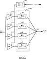
図5Aは、アンプのステージが本来行うべき入力と出力のスイッチング機能を有する、この発明の別の実施形態を示すものである。
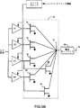
図5Bは、アンプのステージが本来行うべき入力と出力のスイッチング機能を有する、この発明の、さらに別の実施形態を示すものである。
図6は、この発明の効率的なパラレルステージアンプが組み込まれたスペクトラム拡散信号送信機の携帯端末を説明するブロックダイヤグラムを示す図である。
図7は、図6のスペクトラム拡散送信機に含まれるRF送信機の例示的な形態を示す図である。
図8は、低ノイズ信号増幅のために設計された創作力に富んだ実施形態のブロックダイヤグラムである。
図9は、この発明のパラレルステージアンプのシングルステージとして用いられるデュアルトランジスタアンプの概要を説明するものである。
図10は、構成アンプステージのゲインがオフセットされている、この発明のパラレルステージアンプの転移特性を図示するものである。
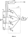
図11は、アンプのステージが本来行うべき入力と出力のスイッチング機能を有する、この発明の、さらに別の実施形態を示すものである。
好ましい実施形態の詳細な説明
I.CDMAセルラ通信への導入
例示的な地上セルラ電話通信システムが、図1に示されている。図1に示されるシステムは、CDMA変調技術をシステム携帯端末のユーザや、セルサイト基地局との間の通信で利用する。各移動機のユーザは、携帯通信機(例えば携帯電話機)を通じて、1あるいはそれ以上のセルサイト基地局と通信し、各携帯通信機は、この発明の効率的パラレルステージアンプを組み入れた送信機を有する。ここでの論議では、「携帯端末」は、この説明を行う目的で、一般に遠隔加入者局に言及するように使用されている。しかしながら、携帯端末は、位置が固定されていてもよいことに留意すべきである。携帯端末は、複数のユーザが集中された加入者システムの部分品である。携帯端末は、音声、データ、あるいはシングルタイプの組み合わせを運ぶのに用いられる。「移動機」という語は、技術語であるが、携帯端末の範囲や機能を限定する意味ではない。
図1において、システムコントローラとスイッチ10は、一般に、セルサイト基地局にシステムコントロール情報を送るための適当なインターフェイスと処理ハードウエアを有する。コントローラ10は、公衆電話交換網(PSTN)から、適当な携帯端末への送信に係わる適当なセルサイト基地局への電話呼出のルーティングを制御する。コントローラ10は、携帯端末からの、少なくとも1つのセルサイト基地局を通じたPSTNへの呼のルーティングを制御する。携帯端末は一般に他の携帯端末と直接通信しないから、コントローラ10は、適当なセルサイト基地局を通じた携帯端末ユーザ間の呼を管理する。
コントローラ10は、専用電話回線や光ファイバリンクといったさまざまな手段により、あるいは無線周波通信によりセルサイト基地局に結合されている。図1においては、例示的な携帯端末16,18と一緒に、2つの例示的なセルサイト基地局12,14を示す。矢印20a,20bと、22a,22bは、それぞれセルサイト基地局12と携帯端末16,18との間の可能な通信リンクを規定している。同様に、矢印24a,24bと、26a,26bは、それぞれセルサイト基地局14と携帯端末16,18との間の可能な通信リンクを規定する。セルサイト基地局12と14は、通常、同じ電力を用いて送信を行う。
携帯端末16は、パス20aと26aを通じてセルサイト基地局12と14から受信した全電力を測定する。同様に、携帯端末18は、パス22aと24aを通じてセルサイト基地局12と14から受信した全電力を測定する。各携帯端末16,18において、信号電力は、信号が広帯域な信号である受信機で測定される。それ故に、この電力測定結果は、疑似雑音(PN)スペクトラム拡散信号を用いた受信信号の相関関係より前に作られる。
携帯端末16がセルサイト基地局12に近づいた時、一般に受信信号電力はパス20aを通じた信号により支配されるであろう。携帯端末16がセルサイト基地局14により近い時は、一般的に受信電力は、パス26aを通じた信号によって支配されるであろう。同様に、携帯端末18がセルサイト基地局14に近づいた時、一般に受信信号電力はパス24aを通じた信号により支配されるであろう。携帯端末18がセルサイト基地局12により近い時は、一般的に受信電力は、パス22aを通じた信号によって支配されるであろう。
携帯端末16,18は、それぞれ、測定結果を用いて、最も近いセルサイト基地局へのパス損失を推定する。携帯端末のアンテナ利得とセルサイト基地局のG/Tの知識とともに、推定されたパス損失は、セルサイト基地局の受信機における所要の搬送波対雑音比を得るために必要とされる公称送信電力を決定するのに用いられる。携帯端末が持つセルサイト基地局パラメータの知識は、メモリに固定されるか、セルサイト基地局情報放送信号であるセットアップチャネルを通じて送信され、特定のセルサイト基地局に関しての公称状態以外を示す。
携帯端末16,18は、セルサイト基地局間を移動する時に、広いダイナミックレンジに対してそれぞれの送信電力を調整する必要が生じる。広いダイナミックレンジにわたる信号増幅が可能な電力アンプは存在するが、関連する利得の変化は、携帯端末の送信機の残りの部分の設計を複雑にする傾向がある。一定に利得を示すことに加えて、携帯端末の送信機のアンプが、対称とするダイナミックレンジ全体にわたって効率的に動作して、バッテリ電力を節約することも要求される。この発明に従えば、高い効率で、線形利得電力アンプが、これらや他の目的を達成する。
II.有効なパラレル電力アンプの概要
次に、図2へ移ると、ここには、この発明のパラレルステージアンプ40の単純化したブロックダイヤグラムが示されている。入力信号、一般的に、ディジタル変調されたRF通信信号は、RF送信変調器(図示しない)から入力ネットワーク44によって受信される。入力ネットワーク44は、入力信号を4つのパラレルアンプステージA1〜A4の少なくとも1つに中継する。最も単純な実施形態では、入力ネットワーク44は、入力信号を選択的にパラレルアンプステージA1〜A4の1つに供給するスイッチマトリックスである。しかしながら、入力ネットワーク44の(図4に見られる)他の構成は、歪みや信号損失を最小化する方法で、入力スイッチングを果たす。好ましい構成では、アンプステージA1〜A4は、それぞれ高周波用電解効果トランジスタ回路かあるいはバイポーラ接合トランジスタ回路の電力アンプを有する。
ステージアンプA1〜A4からの出力は出力ネットワーク48に供給され、このネットワークは、選択されたアンプステージA1〜A4からの増幅されたRF出力信号をアンプ出力端52へ結合する。出力ネットワーク48は、スイッチマトリックスか、それに類似するものを用いて実現されるが、以下に述べる(図4に見られる)出力ネットワーク48の他の構成では、歪みや信号損失を最小化する方法で、入力スイッチングを果たす。増幅されたRF信号は、(図示しない)送信アンテナに供給され、同様にスイッチロジック56に供給される。スイッチロジック56は、出力端52における増幅されたRF信号のレベルを監視し、そして、監視された出力信号レベルを含む範囲に対して出力電力を提供するように設計されたアンプステージA1〜A4を選択するように、入力ネットワーク44と出力ネットワーク48に指示する。他の実施形態では、スイッチロジック56は、関連する基地局からの受信電力レベル、あるいは電力制御コマンドを監視する。
図3に示す好ましい実施形態では、アンプステージA1〜A4は、異なる信号範囲にわたり同じ利得を供給するようにそれぞれバイアスされる。例示的な実施形態では、アンプステージA1は、−23dBmまでの入力信号に応じて、5dBmまでの出力電力に対して、おおよそ28dBの線形利得を供給するようにバイアスされる。同様に、アンプステージA2,A3およびA4は、ステージA1のように、異なる出力信号範囲にわたって同じ線形利得を生成するように、それぞれバイアスされる。具体的には、図3の例示的な実施形態では、アンプステージA2は、−23から−13dBmの間の入力信号に応じて、5〜15dBm範囲にわたる出力信号エネルギを生成し、一方、アンプステージA3,A4は、それぞれ、−13から−4dBmの間、−4から+1dBmの間の入力信号に応じて、15〜24dBm、24〜28dBm範囲にわたる出力信号エネルギを生成する。アンプステージが電解効果トランジスタ回路あるいはバイポーラ接合トランジスタ回路で構成される場合、(図示しない)バイアスネットワークは、特定の出力範囲に対する動作が求められる各アンプステージに、バイアス電流のレベルを供給するのに利用される。図3の利得値と範囲は、特別な例を提供するものであることと、全く異なる入力と出力の電力範囲が、他の実施形態と関連していてもよいことに注意すべきである。
図3の特別な場合について再び考察し、入力信号レベルが増大し、−23dBmに近づくと仮定する。この例では、RF出力信号のレベルがおおよそ5dBmに上昇することをスイッチロジック56が探知するまで、入力信号がアンプステージA1に適用され続ける。この時点において、スイッチロジック56は、アンプステージA2に入力信号を適用するように入力ネットワーク44に指示し、そして、A2からの増幅されたRF出力信号の結果を出力端52に結びつけ始めるように、出力ネットワーク48に通知する。アンプステージA2とA3の間や、アンプステージA3とA4の間における同様の変更は、それぞれ、15および24dbmに近づくRF出力信号レベルにて、スイッチロジック56により制御される。任意的に、スイッチロジック56は、入力信号レベルが過渡的な境界付近で変化する時、隣接アンプステージA1〜A4間における過度のスイッチングを防ぐために、ヒステリシスを提供してもよい。各アンプステージA1〜A4は特定されたRF出力信号範囲にわたって同じ利得を示すように実現されるので、周辺回路素子には、パラレルアンプ40は、出力範囲全体にわたって一定の利得を有する単一のアンプとして見える。出力信号範囲にわたる利得変動を調整する必要性をなくすことから、この発明の特徴は、効果的にRF送信の回路に関する設計を単純化する。なるべくならば、図3で示される個々のアンプステージA1〜A4の1つだけが、一度にONされるのだが、以下に説明する他の実施形態では、必要とされるRF出力を得るために、同時にアンプステージの組み合わせが変えられてON/OFFされる。
図2に示すように、ディジタル変調入力信号内の固有のディジタルワードやシンボル間の境界に関係するタイミング情報は、ローカルコントロールプロセッサからスイッチロジック56に供給される。この発明を別の側面から見ると、スイッチロジック56は、入力信号内のディジタルワードやシンボル間の変化の間に、入力ネットワーク44と出力ネットワーク48とに、アンプステージA1〜A4の異なる一つを選択するように通知する。これは、アンプステージA1〜A4を通る信号パス間の何らかの位相差が、増幅されたRF出力信号によって伝えられる完全なディジタル情報にエラーを生じさせないことを保証する。例えば、以下で述べる典型的なCDMA変調フォーマットでは、ディジタル入力データストリームが、一組の直交ウォルシュコードあるいは「シンボル」を用いて符号化される。この実施形態では、スイッチロジック56はエネーブルされて、入力ネットワーク44と出力ネットワーク48がウォルシュシンボル間の遷移の間だけ、アンプステージA1〜A4間を切り換えるように指示する。典型的な実施形態では、各ウォルシュシンボルの期間は、RF出力電力の切替レートに比べて、非常に短い(例えば、3.25ms)ことから、RF出力信号レベルを異なる出力範囲へクロスさせる時間の直前に、一般に、アンプステージ間をスイッチングするのに多くの機会が利用できる。
図4に移ると、ブロックダイヤグラムは、この発明のパラレルステージアンプ90の他の実施形態を提供するものである。入力信号、一般に、ディジタル変調されたRF通信信号が、第1の直交位相分離器94によって受信される。第1の直交位相分離器94は、入力信号を、同じ大きさで直交位相を持つ一対の入力信号成分に分離する。第1の分離器94からの直交位相信号成分は、第2,第3の直交位相分離器98,102に供給される。第2の分離器98は、直交位相出力を利得調整器G1,G2に供給し、そして、第3の分離器102は、直交位相出力を利得調整器G3,G4に供給する。利得調整器G1〜G4は、それぞれシリアルに、対応する一つの固定利得アンプF1〜F4に接続され、各利得調整器と固定利得アンプのシリアル接続により、可変利得調整アンプステージを形成する。
可変利得調整アンプステージの出力は、第1、第2および第3の直交位相結合器106,110と114の配列を用いて結合される。増幅された出力信号の結果は、(図示しない)送信アンテナに入力され、同様に利得コントロールロジック118にも入力される。利得コントロールロジック118は、可変利得調整アンプステージの種々の組み合わせを選択し、各可変利得調整ステージの利得をセッティングすることによって、アンプ全体の利得をセットするように指示する。図4の一般的な実施形態では、固定利得アンプF1〜F4のそれぞれは、NdBの同じ公称利得を供給するようにバイアスされ、利得調整器G1〜G4は、−3dBの利得/減衰、あるいは0dBにセットされる。これは、可変利得調整アンプステージより選択されたものの利得を以下に示すテーブルIのように設定することにより、RF出力電力の所望されるレベルを与える。

第1,第2および第3の直交位相結合器106,110および114ために、OFFの時はアンプステージの出力インピーダンスは重要ではない。しかしながら、所要のRF出力電力を生成するのに必要なアンプステージF1〜F4だけONにすることにより直流効率は保たれる。
図4に好ましい実施形態を示したが、位相のシフトや結合を用いた他の実施形態も可能であることに注意されたい。例えば、直交位相結合器98および102の直前にそれぞれ配置された2つの利得調整器だけに、利得調整器G1〜G4を置換することができる。その代わりに、1つの利得調整器を直交位相結合器94の直前に配置することもできる。極端なものとしては、利得調整器G1〜G4のすべてを除去でき、そのために、この発明を用いるシステムにおける他の回路の構成部品によりアンプ90の全体の利得の変化を補償する。さらに、直交位相分離器94,98および102、同様に、直交位相結合器106,110および114は、他の型の位相変換器に置き換えることができる。注目すべきは、直交位相分離器および結合器の数が、パラレルアンプステージの数だけ駆動されることである。
今、図5Aを参照すると、さらにこの発明の他の実施形態が示されており、ここには、アンプステージ間の選択が、各ステージに含まれるトランジスタアンプのON/OFFによってなされる。図5Aの実施形態では、各アンプステージA1〜A4は、1つあるいはそれ以上の電解効果トランジスタ回路から構成されていると仮定されている。しかしながら、これらのアンプステージのそれぞれがバイポーラ接合トランジスタかあるいは他の能動回路とすることができることが理解される。所定のステージは、このステージを構成する電解効果トランジスタ回路を作動させることによって選択され、そして所定の電解効果トランジスタ効果をOFFにすることによって選択をやめ、電源がOFFされた電解効果トランジスタの出力インピーダンスを高くして電源がOFFにされた電解効果トランジスタによる逆ローディングを確実に最小化する。このように、ステージの望まれる数の付加的な組み合わせは、各ステージA1〜A4に対する電解効果トランジスタ回路を選択的にON/OFFすることにより達成される。図2の実施形態と対照的に、入力スイッチング機能と出力スイッチング機能は、電解効果トランジスタ回路固有のものである。したがって、スイッチロジック56は、アンプステージA1〜A4を直接制御する。
出力ネットワーク48は、それぞれアンプステージA1〜A4と出力端52との間で接続される整合器66〜69を有する。整合器66〜69は、アンプステージA1〜A4の出力と、出力端52に接続された(図示しない)アンテナとの間に、最適な電力整合を提供する。アンプステージA1〜A4と関連する整合器66〜69との各接続は、ほとんど同程度の信号利得を提供し、そして、これらの各組合わせは、所要レベルの出力電力を達成するのに必要な分だけ、スイッチロジック56によってON/OFFされる。それに応じて、所要レベルの出力電力を生成するのに必要なアンプステージA1〜A4の数だけ、所定の短い時間にONされ、それによって直流電力を維持し、ほとんど一定の効率を維持する。さらには、出力スイッチング機能を成し遂げる個々のアンプステージA1〜A4と、整合器66〜69を備える出力ネットワーク48とを用いることにより、スイッチによる電力損失と信号歪みを避けることができる。
図5Bは、さらに、この発明の他の実施形態を示し、ここでは1つあるいはそれ以上のアンプ利得セルあるいはトランジスタが、アンプステージA1〜A4の出力と中間端72との間に置かれる。図5Bは、図5Aに類似している。しかしながら、各アンプに対応する個々の整合器66〜69に代わって、最終アンプ回路85内のマルチプル利得セル74〜84を有するアンプ回路85は、単一の整合ネットワーク86と対になっている。図5Bに示す典型的な実施形態では、単一利得セルトランジスタ74は、ステージA1と中間端72との間に接続される。同様に、単一利得セルトランジスタ76は、ステージA2と中間端72との間に接続される。対をなす利得セルトランジスタ78,80は、ステージA3と中間端72との間に接続され、そして他の対をなす利得セルトランジスタ82,84は、ステージA4と中間端72との間に接続される。図5Aに示される出力ネットワークと対照的に、図5Bの構成は、単一の最終アンプ回路85を用い、ここで、最終アンプ回路85内の個々の利得セル74〜84は、個別の入力を持つ。これは、物理的な大きさとコストを減少させることができ、そして最終アンプ回路85の構成を単一にできる。図5Aの実施形態のように、もし、利得セル74〜84がバイポーラ接合トランジスタか電解効果トランジスタのどちらかの場合には、これらのバイアスをなくすとそれぞれの出力が高インピーダンス状態となり、最小の実ローディングとなることから、出力スイッチは必要とされない。
各利得セル74〜84は、前述のアンプステージA1〜A4によって供給されるバイアス電流を通じてON/OFFされる。特定の利得セルのトランジスタをON/OFF制御することにより、要求されるレベルの出力電力に調節される。この実施形態において、ステージA3あるいはA4が作動している時に、十分なバイアス電流が生成され、利得セルのトランジスタ(78,80)あるいは(82,84)のそれぞれがONになることに注意すべきである。また、アンプステージA3,A4は、それぞれ別々の2つのセルトランジスタ(78,80)あるいは(82,84)を駆動するが、他の実施形態では、各ステージにて、それ以上、あるいはより少ない利得セルトランジスタを用いてもよいことに注意すべきである。
今、図5Bのアンプの典型的な構成について考えてみると、各利得セルトランジスタ74〜84は、先行するアンプステージA1〜A4によってバイアスがONにされた時に、おおよそ1ワットの電力を供給するように設計されている。テーブルIIは、利得セルのトランジスタの種々の組み合わせが、それぞれアンプステージA1〜A4によってバイアスされONとなった時に、この例示的な構成により生成される、異なるレベルの出力電力を表で示している。テーブルIIを見ると、アンプステージA1あるいはA2のどちらかをONにすることにより、RF出力電力の合計は1ワットだけ増加する一方、アンプステージA3あるいはA4のどちらかをONにすると、RF出力電力の合計は2ワットだけ増加することが分かる。したがって、テーブルIIの方法に従い、4つのアンプステージA1〜A4を用いて、1から6ワットまで変化するRF出力電力レベルを生成するのに図5Bに示した特有の実施形態を使用することができ、これにより所要の出力電力を生成するのに必要なステージだけにバイアスONして直流効率を維持することができる。テーブルIIは単に、例示的な構成を示すもので、そして利得セルトランジスタ74〜84がそれぞれ1ワットより大きくあるいはそれより小さい電力を供給するように設計できることに注意すべきである。しかしながら、同じサイズとなるように各利得セル74〜84を選択することは、最終アンプ回路85の製造を単純化する。
テーブルIIの第1列によって表される図5Bの特定の実施形態においては、もし、アンプステージ1つだけとそれと関係する利得セルトランジスタ、例えばA1とトランジスタ74がバイアスONされ、他のすべてA2〜A4がバイアスOFFされるならば、OFF状態のトランジスタ(76,78,80,82,84)のリアクティブローディングは、単一の出力整合回路86だけを用いた時に、最適な利得整合を供給しないかもしれない。しかしながら、テーブルIIに示した例えば1ワットのような低出力レベルにおいて改善された直流効率が達成される。さらには、選択された個々のアンプステージ、ここではA1において、あるいはこの発明が適用されるシステムにおいて、利得の不整合を調整してもよい。
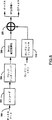
回路1102〜1108の各ゲートは、ブロッキングキャパシタ1112,1114,1116および1118で直流で分離され、入力信号のRF周波数ではつなげられる。スイッチロジック1120は、選択的に直流バイアス電流を、回路1102〜1108のうち、入力信号を増幅するために要求されたものにだけ供給する。このように、入力信号を現在増幅する要求が為された回路にだけバイアスONにすることにより、意味深いことに、直流効率が改善される。この結果、最終ステージアンプの配列が、前述のテーブルIIの構成に類似している。入力整合ネットワーク(図示しない)は、できれば、含まれるすべての回路1102〜1108が作動して最高の能力を発揮するように利用する。
III.デュアルトランジスタアンプステージ
図9は、この発明のパラレルステージアンプ内の1つのステージ(例えばステージA1〜A4の1つ)として用いるのにふさわしいデュアルトランジスタアンプ400の概要を説明するものである。このアンプステージ400は、入力ドライバ電解効果トランジスタ(Q1)と出力ドライバ電解効果トランジスタ(Q2)とを備える。図9では、デュアルゲート電解効果トランジスタ(Q1,Q2)の対がアンプステージ400を含んでいるが、他の実施形態において、他のデバイス技術を用いて実現される単一ゲート電解効果トランジスタ、あるいはバイポーラ接合トランジスタ、あるいはトランジスタが用いられると理解される。
アンプ400に入力される小さな信号は、入力整合ネットワーク404を通じて電解効果トランジスタQ1のゲートに入力され、ここで電解効果トランジスタQ1を通じて電力変換を最適化する。同様に、インターデバイス整合ネットワーク408は、電解効果トランジスタQ1の出力から電解効果トランジスタQ2の入力への電力変換を最大化する。同様の方法で、出力整合ネットワーク412は、電解効果トランジスタQ2の出力インピーダンスとアンプ400によって駆動される負荷(図示しない)との間で最適な電力整合を行う。
電解効果トランジスタQ1とQ2を通じた、穏やかなバイアス電流は、それぞれ直流ゲート電位Vg1とVg2の調整を通じて制御される。一般に、直流ゲート電位Vg1とVg2は、アンプ400が高低の出力電力レベルで一定の利得を示すように、セットされる。図9の実施形態では、入力電解効果トランジスタQ1の次元が、おおよそ8:1の例示的な比率によって出力電解効果トランジスタQ2の対応する次元より小さくなるように選択され、他の構成では、他の比率がよりふさわしいかもしれないことがわかっている。この設計は、アンプ400より求められる出力電力が低い場合にだけに、出力電解効果トランジスタQ2に供給されるバイアス電流を実際に減じるようにすることによって、高められた比率を導く。低い出力電力が求められる場合にだけ、電解効果トランジスタQ2を通じたバイアス電流が、出力電力の中間レベルで必要とされるバイアス電流に比べて、減じられ、そして、電解効果トランジスタQ1を通じたバイアス電流が幾分増加される。より小さい入力電解効果トランジスタQ1は、低出力電力レベルに関して、より大きい出力電解効果トランジスタQ2より効果的に機能することができるから、低電力動作の間に、電解効果トランジスタQ2を通じたバイアス電流を十分に減じることによってアンプ400の効率が増大する。バイアス電流の変化は、直流ゲート電位Vg1とVg2をアナログ的に、あるいは不連続のステップの調整を通じた制御によってなされる。
IV.CDMA携帯端末内の有効な電力アンプ
図6を参照すると、ここでは携帯端末のスペクトラム拡散送信機を説明するブロックダイヤグラムが示され、この送信機には、この発明の有効なパラレルステージアンプが組み込まれている。例示的なCDMAシステムでは、直交信号が、携帯端末と基地局のリンク、すなわち「リバースリンク」にて信号と雑音の好ましい比率を提供するのに用いられる。
図6の送信機において、データビット200は、例えばボコーダによってデータに変換された音声からなり、エンコーダ202に供給され、ここでビットは畳み込み符号化される。データビットレートが、エンコーダ202のビット処理レート以下の時、エンコーダ202の動作レートに一致するビットレートで、復元データストリームを生成するために、エンコーダ202が入力データビット200を繰り返すのに、コードシンボルの復元が用いられる。例示的な実施形態では、エンコーダ202は、データビット200を、公称11.6kbits/secのビットレート(Rb)で受信し、そして、Rb/r=34.8symbols/secを生成し、ここで「r」は、エンコーダ202のコードレート(例えば1/3)を示す。符号化されたデータは、この時、ブロックインターリーバ204に供給され、ここでブロックインターリーブされる。
64−ary直交変調器206には、64キャラクタが存在しうる場合に、(1/r)(Rb/log264)=5800characters/secのレートで、log264=6シンボルを含むキャラクタにグループ化される。好ましい実施形態では、各キャラクタは、64のウォルシュシーケンス長に符号化される。各ウォルシュシーケンスは、64バイナリビット、あるいは「チップ」を有し、ここには長さ64の64ウォルシュコードのセットがある。64直交コードは、64ハダマードマトリックスによる64からのウォルシュコードに一致し、ここではウォルシュコードは、一例、あるいはマトリックスのコラムである。
変調器206によって生成されたウォルシュシーケンスは、エクスクルーシブORコンバイナ208に供給されるように見え、それからここでは、コンバイナにて、特定の携帯端末に対する特定のPNコードを用いて、「covered」、あるいは乗算される。このような「long」PNコードは、ユーザPNロングコードマスクに従って、Rcレートで、PNロングコードジェネレータ210により生成される。例示的な実施形態では、ロングコードジェネレータ210は、1ウォルシュチップあたり4PNチップを生成するために、例示的には1.2288MhzのチップレートRcで動作する。この発明に従って、携帯端末の送信機内の有効なパラレルステージアンプが、各ウォルシュコードシンボルの境界(すなわち、連続するコードシンボルのPNチップのうち、最後のシンボルの後、およびはじめのシンボルより前)にて、PNチップ間だけで状態を変えることが許される。
図7を参照すると、RF送信機250の例示的な構成が示されている。符号分割多元接続(CDMA)スペクトラム拡散の応用において、一対のショートPNシーケンス、PNIとPNQは、それぞれPNIジェネレータ252とPNQジェネレータ254とにより、エクスクルーシブORコンバイナ256と258に供給される。PNIとPNQのシーケンスは、それぞれin位相(I)と直交位相(Q)の通信チャネルに関係し、そして一般に各ユーザロングPNコードの長さよりも短い長さ(32768チップ)である。結果として生じたIチャネル符号拡散シーケンス260とQチャネル符号拡散シーケンス262は、それぞれベースバンドフィルタ264と266を通過する。
ディジタル・アナログ(D/A)コンバータ270と272は、ディジタルIチャネルとディジタルQチャネルの情報を、それぞれアナログ形式に変換する。D/Aコンバータ270と272によって生成されたアナログ波形は、それぞれ局部発振器(LO)搬送波周波数信号Cos(2πft)とSin(2πft)とともに、ミキサ288と290に供給され、ここで、これらはミキシングされ加算器292に供給される。直交位相搬送波信号Cos(2πft)とSin(2πft)は、適当な周波数源(図示しない)から供給される。これらミキシングされたIF信号は、加算器292にて加算され、ミキサ294に供給される。
ミキサ294は、RF周波数帯にアップコンバートするために、加算された信号を周波数シンセサイザ296からのRF周波数信号とミキシングする。この時、このRF信号は、バンドパスフィルタ298でフィルタリングされ、そして、この発明の有効なパラレルステージRFアンプ299に供給される。再び説明すると、携帯端末のコントローラは、各ウォルシュコードシンボル間の転移を規定するPNチップ間だけに、アンプ299内のアンプステージの選択された組み合わせを変えることができるようにすることによって適当な位相が確実に保持されるようにする。
V.CDMA携帯端末におけるデュアルステージパラレルアンプ
図8は、図6および図7に示され、前述したCDMA携帯端末における広いダイナミックレンジにわたって信号増幅を行うように設計されたパラレルステージアンプ310のブロックダイアグラムである。アンプ310は、低出力アンプ(LPA)313と高出力アンプ(HPA)316、第1と第2のスイッチ(318,322)で表される出力スイッチマトリックス、第1と第2のダミー負荷(320,324)、およびスイッチロジック334とによって表されるパラレルアンプステージを備える。簡単に説明すると、アンプ310は、低レベルの出力電力だけが求められる時に、低レベルの直流電流が流れるLPA313を排他的にだけ利用し、また、高レベルの出力電力が求められる時に、HPA316を排他的に利用することにより、改善された直流効率をもたらす。この効率は、第1と第2のダミー負荷(320,324)と、アンテナ(図示しない)とに、LPA313とHPA316の各出力を二者択一で出力する指示をスイッチロジック334が行うことによってなされる。低出力指示の際には、スイッチロジック334は、第1のスイッチ318に対して、HPA316の出力を第1のダミー負荷320に供給するように指示し、そして、第2のスイッチ322に対して、LPA313の出力をアンテナ(図示しない)に供給するように指示する。さらに多くの送信電力が求められるならば、HPA316は、LPA313によって送信されているのと同じ電力を生成し始め、HPA316の出力は、第1のダミー負荷320に入力して捨てられる。適切なスイッチング境界にて、スイッチロジック334は、第1のスイッチ318に対して、HPA316の出力をアンテナ(図示しない)に供給するように指示し、そして、第2のスイッチ322に対して、LPA313の出力を第2のダミー負荷324に供給するように指示する。
好ましい実施形態においては、LPA313は、低出力モード動作時にAクラスアンプとして機能する。すなわち、LPA313が、圧縮されていない時に供給されるRF入力信号のレベルとは無関係にLPA313は電力利得を供給する。さらに、Aクラスアンプとして、LPA313は、圧縮されていない限り、RF出力電力レベルに関係なく、ほとんど一定の直流電力を消費する。低出力モード動作時には、アンテナに供給される出力電力レベルは、LPA313に供給されるRF入力電力のレベルを調整することにより実質的に制限される。なぜなら、LPA313は、低出力モード動作時に、一様な利得を供給し、最小の歪みで入力電力をリニアに追跡するので、LPA313によって生成されるRF出力電力レベルは、LNA312に先行するAGCアンプ(図示しない)によって効率よく制御される。
この発明にしたがうと、HPA316の出力に現れる出力電力は、低出力動作モードと高出力動作モードの間の何らかの切り替え直前の転移期間に、LNA313によって生成される出力電力に整合される。特に、転移期間では、HPA316によって生成される電力は、利得制御ループ326によって監視される。利得制御ループ326は、転移期間のHPA316の利得をアンプ313の利得と等しくなるように設定することにより、LNA313とHPA316の出力における電力レベルを一様にする。このような「境目のない」転移が、低出力モードから高出力モードへ、およびこの逆でも達成される。例示的なCDMAの構成では、スイッチロジック334は、スイッチ318と322がウォルシュ符号シンボルの境界でトグル切り替えされることだけを許容する。
高出力モードの間には、HPA316は、本質的に、ABクラスか、あるいはBクラスのアンプとして動作する。すなわち、アンプ316の電力利得と直流電力消費は、RF入力電力レベルの関数である。好ましい構成では、HPA316は、少なくとも、1つの電解効果トランジスタを備える。電解効果トランジスタアンプのゲート電圧は、電解効果トランジスタと電解効果トランジスタ利得によって導かれた電流の総量に影響を及ぼし、より高い直流効率は、ある動作レベルに対して要求される最小電解効果トランジスタ電流を要求されるRF出力電力レベルに整合させることによって、達成されるはずである。HPA316の利得は、要求される動作範囲で非線形であるから、アンプ310によって生成されるRF信号のレベルは、HPA316に供給される信号レベルをもっぱら調整することによって制御されないかもしれない。むしろ、利得制御ループ326は、RF電力レベルの要求されるレベルがアンテナに伝えられるように、HPA316の利得を設定する。
図8に示すように、利得制御ループ326は、HPA316の出力に接続される検出器/バッファ340を有する。検出器/バッファ340は、動作アンプ344とキャパシタ346から構成されているループ積分器を駆動する。HPA316は、一般に1つかそれ以上の電解効果トランジスタアンプを備えているから、電流アンプ348は、必須の電解効果トランジスタアンプバイアス電流を供給するために、制御ループ326内に備えられる。電力制御ループ326は、HPA316のゲートとドレインの電圧を制御することによって、検出器/バッファ340によって測定されるようなHPA316のRF出力電力を設定する。この方法では、AGCアンプ(図示しない)により設定されるようなHPA316への入力電力が出力要求の増大に連れて増大し続けるが、HPA316の出力電力が利得制御ループ326によって設定され続けるので、HPA316の非線形性は克服される。
CDMA送信機に含まれるのにふさわしいアンプ310の例示的な構成において、利得制御ループ326はスイッチ352を備えてもよく、このスイッチは、「ブランク」のフレームの期間に開かれ、この間では、アンプ310によって信号電力がアンテナに供給されない。このようなブランクフレームは、全体的なデータ送信レートがフルレートより遅いレートの時に、実データのアクティブフレームの間に挟まれる。スイッチ352は、各ブランクフレームの開始に先んじて、積分ループを開放し、それに続くアクティブフレームの開始後に、即座にループを閉じる。
VI.利得オフセットパラレルステージ
図10は、この発明のパラレルステージアンプの特性を変化を図で説明するもので、構成するアンプステージは利得においてオフセットされている。簡便のために、図10のバイアス技術は、図2で示されたパラレルステージアンプを参照して述べることにする。図10に例示されたバイアス方法において、各アンプステージA1〜A4は、異なる利得で実現される。ステージ間のスイッチングは、前述した方法で生じるが、ステージ間の利得オフセットは、増幅されたRF出力信号の電力の変化は不連続となる。前述したように、スイッチロジック56(図2)は、出力端52における、増幅されたRF信号のレベルを監視する。この時、スイッチロジック56は、監視された出力信号レベルで動作するように設計された適切なステージA1〜A4を選択するように、入力スイッチマトリックスと出力ネットワーク48に指示する。
図10を参照すると、アンプステージA1〜A4は、予め定められた範囲内で入力信号に応じて線形の利得を提供するようにそれぞれバイアスされる。特に、アンプステージA1は、PIN,0とPIN,1の間の入力信号に応じて、POUT,0からPOUT,1までの範囲の出力信号にわたり、線形利得を生成するようにバイアスされる。同様に、アンプステージA2,A3およびA4は、それぞれPOUT,1からPOUT,2まで、POUT,2からPOUT,3まで、POUT,3からPOUT,4までの範囲の出力信号にわたり、線形利得を生成するようにバイアスされる。アンプステージが電解効果トランジスタかあるいはバイポーラ接合トランジスタ回路で構成される時、バイアスネットワーク(図示しない)は、特定の出力範囲に対する動作で要求される各アンプステージへのバイアス電流のレベルを供給するのに用いられる。
図10によって意図されたステージ間の利得オフセットは、例えば、パラレルステージ電力アンプとともに用いられるAGC回路に要求されるダイナミックレンジを減少させる要求がある時に有用である。低出力レベルで示される減少された利得は、信号対雑音比がたいてい最小となる、低入力信号レベルでより少ない雑音増幅となることも重要である。それゆえに、図10の利得オフセット技術は、低入力信号レベルでの雑音性能を改善するのに、有効に用いられるとともに、完成したアンプチェーンの全体にわたる雑音性能を改善するのに用いられる。
好ましい実施形態の先の説明は、当業者が本発明を生産または使用できるように提供されている。これらの実施形態に対するさまざまな修正は当業者にとって容易に明らかとなるであろう。ここに規定されている一般的な原理は発明力を使用することなく他の実施形態に対して適用することができる。したがって、本発明はここに示されている実施形態に制限されることを意図しているものでなく、ここに開示されている原理および新規な特徴と矛盾しない最も広い範囲に一致すべきものである。Background of the Invention
I. Field of Invention
The present invention relates to a signal amplifier. In particular, the present invention relates to a method and circuit arrangement for providing efficient linear signal amplification over a wide dynamic range by using various parallel amplification devices.
II. Explanation of related technology
The use of code division multiple access (CDMA) modulation techniques is one of several techniques that facilitate communication in large systems with many users. Other techniques such as time division multiple access (TDMA), frequency division multiple access (FDMA), amplitude modulation (AM), and modulation schemes such as amplitude compressed single sideband (ACSSB) are known, but CDMA Has significant advantages over these techniques. The use of CDMA technology in a multiple access communication system is disclosed in US Pat. No. 4,901,307 entitled “SPREAD SPECTRUM MULTIPLE ACCESS COMMUNICATION SYSTEM USING SATELLITE OR TERRESTRIAL REPEATERS”, which is assigned to the assignee of the present invention. Incorporated here for reference.
The above-mentioned patent discloses multiple access technology, in which multiple users, each having a transceiver, use a code division multiple access (CDMA) spread spectrum communication signal to transmit a satellite repeater or (or cell). It communicates through ground base stations (also known as site stations and short cell sites). When using CDMA communication, the frequency spectrum can be reused many times, which allows for an increase in system user tolerance. The use of CDMA exhibits higher spectrum efficiency than when other multiple access communications are used. Increasing system capacity in a CDMA system may be realized by controlling the transmit power of mobile terminals communicating with each user in order to reduce interference to other system users. In a terrestrial CDMA cellular communication system, it is highly desirable to maximize the tolerances for simultaneous communication links that can be supported by the required system bandwidth. Maximize system capacity if each mobile device's transmit power is controlled so that the transmitted signal reaches the cell site receiver with a minimal signal-to-noise interference ratio that allows acceptable data recovery can do. If the transmitted signal from the mobile terminal reaches the cell site receiver at a power level that is too low, the bit error rate is too high and high quality communication is not guaranteed. On the other hand, if an acceptable communication is established by setting the mobile terminal transmission signal to a power level that is too high when received at the cell site receiver, other mobile terminal transmissions sharing the same channel, ie the same bandwidth Interference with signal occurs. This interference adversely affects other mobile terminals and reduces the total number of mobile terminals that communicate.
The signal received from each portable terminal is measured at the cell site base station, and the measurement result is compared with the required power level. Based on this comparison, the cell site base station determines a deviation from the received power level necessary to maintain the desired communication. The required power level is preferably the minimum power level required to maintain high quality communications that reduce system interference.
At that time, the cell site base station transmits a power control command signal to each system user so as to adjust, or “fine-tune”, the transmission power of the mobile terminal. This command signal is used by the mobile terminal to change the transmission power to approach the level required to maintain reverse link communication between the mobile terminal and the cell site base station. In general, when the channel state changes due to movement of the mobile terminal, the power measurement of the receiver of the mobile terminal and the power control feedback from the cell site base station are both frequently used to maintain an appropriate power level. Readjust the transmit power.
The use of this type of power control technology requires that the mobile terminal operate linearly over a relatively wide dynamic range. Since real mobile terminals operate on battery power, it is necessary for the transmit power amplifier to be able to operate efficiently linearly over the typical dynamic range of a CDMA communication system. Conventional power amplifiers of both variable gain and fixed gain lack the essential capability and linearity over a wide dynamic range, and there is a need for a power amplifier that can exhibit this type of performance.
Summary of invention
In general, the present invention uses a form of an amplifier circuit that supplies an amplified signal in response to an input signal in a manner that improves efficiency while maintaining linearity. The amplifier circuit includes an input switch for applying an input signal to a selected one of the first and second parallel connected amplification stages, wherein the first amplification stage is a first input signal. The second amplification stage is biased to provide a constant gain over the dynamic range of the second input signal. An output network is provided for combining amplified signals from selected amplification stages.
In a preferred embodiment, the output network has an output switch for connection to the output end of the selected amplification stage, and further has a power measurement circuit for measuring the power of the amplified signal. When the power measurement result of the amplified output signal is out of the preset output range, the switch control circuit is used to perform control for connecting the input switch and the output switch to another amplification stage. In particular, when using the present invention in a digital transmitter, the switch control circuit causes the input switch matrix and output network to have one of the different amplification stages only during the transition period between digital words or symbols in the input signal. Allow to choose.
In one embodiment, the input signal is supplied directly to the different final stage transistor devices. The gates of this device are isolated in direct current by a blocking capacitor, but are tied together when the input signal is at a frequency in the RF band. The switch logic selectively supplies DC bias current only to devices that require amplification of the input signal. Thus, direct current efficiency is significantly improved by biasing only devices that require amplification of the input signal.
[Brief description of the drawings]
The features and advantages of the present invention will become more apparent from the detailed description set forth below when taken in conjunction with the drawings in which like reference characters identify correspondingly throughout.
FIG. 1 is a schematic diagram of an exemplary cellular telephone system having a base station device and a plurality of mobile terminals located in at least one cell.
FIG. 2 shows a simplified block diagram of the parallel stage amplifier of the present invention.
FIG. 3 shows, by way of illustration, an exemplary mechanism for biasing the amplification stages A1-A4 in the parallel stage amplifier of FIG.
FIG. 4 is a block diagram of another embodiment of the parallel stage amplifier of the present invention.
FIG. 5A shows another embodiment of the present invention in which the amplifier stage has the input and output switching functions that should be performed.
FIG. 5B shows yet another embodiment of the present invention in which the amplifier stage has input and output switching functions that should be performed.
FIG. 6 is a block diagram for explaining a portable terminal of a spread spectrum signal transmitter incorporating the efficient parallel stage amplifier of the present invention.
FIG. 7 is a diagram illustrating an exemplary form of an RF transmitter included in the spread spectrum transmitter of FIG.
FIG. 8 is a block diagram of a creative embodiment designed for low noise signal amplification.
FIG. 9 explains the outline of a dual transistor amplifier used as a single stage of the parallel stage amplifier of the present invention.
FIG. 10 illustrates the transfer characteristics of the parallel stage amplifier of the present invention in which the gain of the component amplifier stage is offset.
FIG. 11 shows still another embodiment of the present invention in which an amplifier stage has an input / output switching function that should be originally performed.
Detailed Description of the Preferred Embodiment
I. Introduction to CDMA cellular communication
An exemplary terrestrial cellular telephone communication system is shown in FIG. The system shown in FIG. 1 uses a CDMA modulation technique for communication with a user of a system portable terminal and a cell site base station. A user of each mobile device communicates with one or more cell site base stations through a portable communication device (eg, a cellular phone), and each portable communication device has a transmitter incorporating the efficient parallel stage amplifier of the present invention. Have. In this discussion, “portable terminal” is generally used to refer to a remote subscriber station for purposes of this description. However, it should be noted that the position of the mobile terminal may be fixed. A portable terminal is a part of a subscriber system in which a plurality of users are concentrated. Mobile terminals are used to carry voice, data, or single type combinations. The term “mobile device” is a technical term, but does not mean to limit the range and functions of the mobile terminal.
In FIG. 1, the system controller and switch 10 generally have suitable interfaces and processing hardware for sending system control information to the cell site base station. The
The
The portable terminal 16 measures the total power received from the cell
When the mobile terminal 16 approaches the cell
Each of the
When the
II. Overview of valid parallel power amplifiers
Turning now to FIG. 2, there is shown a simplified block diagram of the
Outputs from stage amplifiers A1-A4 are provided to
In the preferred embodiment shown in FIG. 3, the amplifier stages A1-A4 are each biased to provide the same gain over different signal ranges. In the exemplary embodiment, amplifier stage A1 is biased to provide a linear gain of approximately 28 dB for output power up to 5 dBm in response to input signals up to −23 dBm. Similarly, amplifier stages A2, A3 and A4 are each biased to produce the same linear gain over different output signal ranges, like stage A1. Specifically, in the exemplary embodiment of FIG. 3, amplifier stage A2 generates output signal energy ranging from 5 to 15 dBm in response to an input signal between −23 and −13 dBm, while amplifier stage A3 and A4 generate output signal energy ranging from 15 to 24 dBm and 24 to 28 dBm depending on the input signal between -13 and -4 dBm and between -4 and +1 dBm, respectively. When the amplifier stage is composed of a field effect transistor circuit or a bipolar junction transistor circuit, a bias network (not shown) is used to supply a level of bias current to each amplifier stage that is required to operate for a specific output range. Is done. It should be noted that the gain values and ranges in FIG. 3 provide a special example and that completely different input and output power ranges may be associated with other embodiments.
Consider again the special case of FIG. 3 and assume that the input signal level increases and approaches -23 dBm. In this example, the input signal continues to be applied to amplifier stage A1 until
As shown in FIG. 2, timing information relating to the boundaries between unique digital words and symbols within the digitally modulated input signal is provided to the
Turning to FIG. 4, the block diagram provides another embodiment of the
The output of the variable gain adjustment amplifier stage is combined using an array of first, second and
Because of the first, second and
Although the preferred embodiment is shown in FIG. 4, it should be noted that other embodiments using phase shifting and coupling are possible. For example, the gain adjusters G1 to G4 can be replaced with only two gain adjusters respectively disposed immediately before the
Referring now to FIG. 5A, still another embodiment of the present invention is shown, where the selection between amplifier stages is made by turning on / off transistor amplifiers included in each stage. In the embodiment of FIG. 5A, it is assumed that each amplifier stage A1-A4 is composed of one or more field effect transistor circuits. However, it is understood that each of these amplifier stages can be a bipolar junction transistor or other active circuit. The predetermined stage is selected by operating the field effect transistor circuit that constitutes this stage, and the selection is stopped by turning off the field effect transistor effect, and the output impedance of the field effect transistor whose power is turned off. To ensure that the reverse loading due to the field effect transistor with the power turned off is minimized. Thus, the desired number of additional combinations of stages is achieved by selectively turning on / off the field effect transistor circuits for each stage A1-A4. In contrast to the embodiment of FIG. 2, the input switching function and the output switching function are specific to the field effect transistor circuit. Therefore, the
The
FIG. 5B further illustrates another embodiment of the present invention, in which one or more amplifier gain cells or transistors are placed between the outputs of amplifier stages A1-A4 and
The
Considering now the typical configuration of the amplifier of FIG. 5B, each gain cell transistor 74-84 supplies approximately 1 watt of power when biased on by the preceding amplifier stages A1-A4. Designed to be Table II tabulates the different levels of output power produced by this example configuration when various combinations of gain cell transistors are biased ON by amplifier stages A1-A4, respectively. . Looking at Table II, turning on either amplifier stage A1 or A2 increases the total RF output power by 1 watt, while turning on either amplifier stage A3 or A4 turns on RF output power. It can be seen that the total increases by 2 watts. Thus, according to the method of Table II, the specific embodiment shown in FIG. 5B can be used to generate RF output power levels that vary from 1 to 6 watts using four amplifier stages A1-A4. As a result, it is possible to maintain the DC efficiency by turning on the bias only for the stages necessary to generate the required output power. It should be noted that Table II merely shows an exemplary configuration, and that the gain cell transistors 74-84 can each be designed to supply greater than or less than 1 watt. However, selecting each gain cell 74-84 to be the same size simplifies the manufacture of the
In the particular embodiment of FIG. 5B represented by the first column of Table II, if only one amplifier stage and its associated gain cell transistor, eg, A1 and
The gates of the
III. Dual transistor amplifier stage
FIG. 9 illustrates an outline of a
A small signal input to
The gentle bias currents through the field effect transistors Q1 and Q2 are respectively DC gate potential V g1 And V g2 It is controlled through adjustment. Generally, DC gate potential V g1 And V g2 Is set so that
IV. Effective power amplifier in CDMA portable terminal
Referring to FIG. 6, there is shown a block diagram illustrating a spread spectrum transmitter of a mobile terminal, which incorporates an effective parallel stage amplifier of the present invention. In an exemplary CDMA system, orthogonal signals are used to provide a favorable signal to noise ratio on the mobile terminal to base station link, or “reverse link”.
In the transmitter of FIG. 6, the
In the 64-
The Walsh sequence generated by the
Referring to FIG. 7, an exemplary configuration of the
Digital / analog (D / A)
The
V. Dual stage parallel amplifier in CDMA portable terminal
FIG. 8 is a block diagram of a
In the preferred embodiment,
In accordance with the present invention, the output power appearing at the output of
During the high power mode, the
As shown in FIG. 8, the
In an exemplary configuration of an
VI. Gain offset parallel stage
FIG. 10 is a diagram illustrating changes in the characteristics of the parallel stage amplifier according to the present invention, and the amplifier stage is offset in gain. For simplicity, the bias technique of FIG. 10 will be described with reference to the parallel stage amplifier shown in FIG. In the bias method illustrated in FIG. 10, the amplifier stages A1 to A4 are realized with different gains. Although switching between stages occurs in the manner described above, the gain offset between stages makes the power change of the amplified RF output signal discontinuous. As described above, the switch logic 56 (FIG. 2) monitors the level of the amplified RF signal at the
Referring to FIG. 10, amplifier stages A1-A4 are each biased to provide a linear gain in response to an input signal within a predetermined range. In particular, the amplifier stage A1 is P IN, 0 And P IN, 1 Depending on the input signal between OUT, 0 To P OUT, 1 Biased to produce linear gain over a range of output signals. Similarly, amplifier stages A2, A3, and A4 are respectively connected to P OUT, 1 To P OUT, 2 Until P OUT, 2 To P OUT, 3 Until P OUT, 3 To P OUT, 4 Biased to produce linear gain over a range of output signals. When the amplifier stage is composed of field effect transistors or bipolar junction transistor circuits, a bias network (not shown) provides the level of bias current to each amplifier stage required for operation over a specific output range. Used.
The gain offset between stages intended by FIG. 10 is useful when there is a need to reduce the dynamic range required for AGC circuits used with, for example, parallel stage power amplifiers. It is also important that the reduced gain exhibited at low power levels results in less noise amplification at low input signal levels, where the signal-to-noise ratio is usually minimized. Therefore, the gain offset technique of FIG. 10 is used effectively to improve noise performance at low input signal levels and to improve the overall noise performance of the finished amplifier chain.
The previous description of the preferred embodiments is provided to enable any person skilled in the art to make or use the present invention. Various modifications to these embodiments will be readily apparent to those skilled in the art. The general principles defined herein can be applied to other embodiments without using inventive power. Accordingly, the present invention is not intended to be limited to the embodiments shown herein, but is to be accorded the widest scope consistent with the principles and novel features disclosed herein. .
Claims (8)
無線周波数入力信号の部分間の境界を表すタイミング情報を受信するタイミング情報入力線と、
前記無線周波数入力信号を増幅する複数のアンプステージであって、この複数のアンプステージはそれぞれ、前記無線周波数入力信号を受信するアンプステージ入力と増幅された無線周波数信号を供給するアンプステージ出力とを備え、直流電流バイアスがそのそれぞれのアンプステージ入力に適用されている間にのみ無線周波数入力信号を増幅するように動作する複数のアンプステージと、
前記複数のアンプステージの各アンプステージ入力と、タイミング情報入力線とに接続され、作動すべき特定のアンプステージを選択し、直流電流バイアスを、選択されたアンプステージ入力のそれぞれのアンプ入力ステージに供給し、無線周波数入力信号の部分間の境界の間でのみ特定のアンプステージの選択を変化させるよう動作するコントロール回路と、
前記アンプステージ入力のそれぞれに接続され、前記複数のアンプステージの他の一つのアンプ入力ステージから前記直流電流バイアスを分離する手段とを具備し、
前記境界は、無線周波数入力信号に施されるウォルシュコード間の遷移の期間を構成することを特徴とする増幅回路。 In an amplifier circuit for supplying a signal amplified in response to a radio frequency input signal having a continuous portion divided by a signal boundary in a mobile station of a code division multiple access system ,
A timing information input line for receiving timing information representing a boundary between portions of the radio frequency input signal;
A plurality of amplifier stages for amplifying the radio frequency input signal, each of the plurality of amplifier stages having an amplifier stage input for receiving the radio frequency input signal and an amplifier stage output for supplying an amplified radio frequency signal. A plurality of amplifier stages that operate to amplify the radio frequency input signal only while a DC current bias is applied to its respective amplifier stage input;
Each amplifier stage input of the plurality of amplifier stages and a timing information input line are connected to select a specific amplifier stage to be operated, and a direct current bias is applied to each amplifier input stage of the selected amplifier stage input. A control circuit that operates to supply and change the selection of a particular amplifier stage only between the boundaries between portions of the radio frequency input signal;
Means for connecting to each of the amplifier stage inputs and separating the DC current bias from one other amplifier input stage of the plurality of amplifier stages ;
2. The amplifier circuit according to claim 1, wherein the boundary constitutes a transition period between Walsh codes applied to a radio frequency input signal .
前記アンプステージ出力のそれぞれに接続され、前記複数のアンプステージの選択された少なくとも一つからの前記増幅された信号を出力ネットワークの出力端に供給する出力ネットワークとを備えることを特徴とする請求項1に記載の増幅回路。An input network comprising an input connected to the input signal and a plurality of outputs, each output connected to one of the amplifier stage inputs, and supplying the input signal to each of the plurality of amplifier stages;
And an output network connected to each of the amplifier stage outputs and supplying the amplified signal from at least one selected of the plurality of amplifier stages to an output end of an output network. 2. The amplifier circuit according to 1.
無線周波数入力信号の部分間の境界を表すタイミング情報を受信する工程と、
前記入力信号を、前記複数のアンプステージのそれぞれに適用する工程と、
信号を増幅する際に使用する増幅ステージを選択する工程と、
選択されたアンプステージに、無線周波数入力信号の部分間の境界の間で開始される直流電流バイアス信号を適用する工程と、
前記直流バイアス信号を、前記選択された一つを除く、すべての前記複数の他のアンプステージから分離する工程と、
前記増幅された信号を生成するために、前記選択されたアンプステージにて、前記入力信号を増幅する工程と、
前記増幅された信号を出力端に供給する工程とを具備し、
前記境界は、無線周波数入力信号に施されるウォルシュコード間の遷移の期間を構成することを特徴とする方法。 In a mobile station of a code division multiple access system, a continuous portion divided by signal boundaries in an amplifier circuit comprising a plurality of amplifier stages that operate to amplify the signal only while simultaneously receiving a DC current bias signal In a method for providing an amplified signal in response to a radio frequency input signal having:
Receiving timing information representing a boundary between portions of the radio frequency input signal;
Applying the input signal to each of the plurality of amplifier stages;
Selecting an amplification stage to be used when amplifying the signal;
Applying to the selected amplifier stage a direct current bias signal initiated between the boundaries between the portions of the radio frequency input signal;
Separating the DC bias signal from all of the plurality of other amplifier stages except the selected one;
Amplifying the input signal at the selected amplifier stage to generate the amplified signal;
Providing the amplified signal to an output end ,
The method wherein the boundary constitutes a period of transition between Walsh codes applied to a radio frequency input signal .
Applications Claiming Priority (3)
| Application Number | Priority Date | Filing Date | Title |
|---|---|---|---|
| US08/767,124 | 1996-12-09 | ||
| US08/767,124 US5872481A (en) | 1995-12-27 | 1996-12-09 | Efficient parallel-stage power amplifier |
| PCT/US1997/022113 WO1998026503A1 (en) | 1996-12-09 | 1997-12-05 | Efficient parallel-stage power amplifier |
Publications (3)
| Publication Number | Publication Date |
|---|---|
| JP2001524275A JP2001524275A (en) | 2001-11-27 |
| JP2001524275A5 JP2001524275A5 (en) | 2005-08-11 |
| JP4024867B2 true JP4024867B2 (en) | 2007-12-19 |
Family
ID=25078550
Family Applications (1)
| Application Number | Title | Priority Date | Filing Date |
|---|---|---|---|
| JP52679198A Expired - Lifetime JP4024867B2 (en) | 1996-12-09 | 1997-12-05 | Efficient parallel stage power amplifier |
Country Status (12)
| Country | Link |
|---|---|
| US (1) | US5872481A (en) |
| EP (1) | EP0941575B1 (en) |
| JP (1) | JP4024867B2 (en) |
| KR (1) | KR100560335B1 (en) |
| CN (1) | CN1148870C (en) |
| AU (1) | AU724403B2 (en) |
| BR (1) | BR9713881B1 (en) |
| CA (1) | CA2273151C (en) |
| DE (1) | DE69727962T2 (en) |
| HK (1) | HK1022794A1 (en) |
| IL (1) | IL130120A (en) |
| WO (1) | WO1998026503A1 (en) |
Families Citing this family (190)
| Publication number | Priority date | Publication date | Assignee | Title |
|---|---|---|---|---|
| US6678311B2 (en) | 1996-05-28 | 2004-01-13 | Qualcomm Incorporated | High data CDMA wireless communication system using variable sized channel codes |
| US6208846B1 (en) * | 1997-01-13 | 2001-03-27 | Lucent Technologies, Inc. | Method and apparatus for enhancing transmitter circuit efficiency of mobile radio units by selectable switching of power amplifier |
| JP3171141B2 (en) * | 1997-06-06 | 2001-05-28 | 日本電気株式会社 | Mobile communication transmitter and control method thereof |
| JP3094955B2 (en) * | 1997-06-23 | 2000-10-03 | 日本電気株式会社 | Transmission amplifier control circuit |
| DE69819677T2 (en) * | 1998-02-19 | 2004-09-30 | Stmicroelectronics S.R.L., Agrate Brianza | Connect a capacitance to a mutually exclusively selected integrated amplifier from a large number of integrated amplifiers |
| GB9805148D0 (en) * | 1998-03-11 | 1998-05-06 | Philips Electronics Nv | Radio receiver |
| US6060949A (en) * | 1998-09-22 | 2000-05-09 | Qualcomm Incorporated | High efficiency switched gain power amplifier |
| US6625430B2 (en) * | 1998-12-15 | 2003-09-23 | Ericsson Inc. | Method and apparatus for attaining higher amplifier efficiencies at lower power levels |
| US6066983A (en) * | 1998-12-21 | 2000-05-23 | At&T Corp | PCS multi-carrier linear power amplifier |
| US6615028B1 (en) * | 1998-12-29 | 2003-09-02 | Skyworks Solutions, Inc. | System and method for selecting amplifiers in a communications device |
| US6594303B1 (en) * | 1999-01-11 | 2003-07-15 | Qualcomm Incorporated | Coherent demodulator for use in the presence of phase discontinuities |
| JP2000286652A (en) * | 1999-03-31 | 2000-10-13 | Harada Ind Co Ltd | Controller |
| US6118343A (en) * | 1999-05-10 | 2000-09-12 | Tyco Electronics Logistics Ag | Power Amplifier incorporating single drain switch and single negative voltage generator |
| US6763470B1 (en) * | 1999-05-19 | 2004-07-13 | Globespanvirata, Inc. | System and method for dynamically amplifying a delayed analog signal based on amplitude information obtained from its digital representation |
| US6799020B1 (en) | 1999-07-20 | 2004-09-28 | Qualcomm Incorporated | Parallel amplifier architecture using digital phase control techniques |
| WO2001011768A1 (en) * | 1999-08-10 | 2001-02-15 | Siemens Aktiengesellschaft | Method and device for operating a radio frequency power amplifier |
| US6518856B1 (en) * | 1999-10-13 | 2003-02-11 | Signal Technology Corporation | RF power divider/combiner circuit |
| JP2001203540A (en) | 2000-01-19 | 2001-07-27 | Hitachi Ltd | High frequency power amplifier |
| US6300828B1 (en) | 2000-01-20 | 2001-10-09 | Next Level Communications | Switchless high efficiency amplifier |
| WO2001056171A2 (en) * | 2000-01-25 | 2001-08-02 | Paradigm Wireless Communications, Llc | Switch assembly with a multi-pole switch for combining amplified rf signals to a single rf signal |
| GB2359206B (en) * | 2000-02-08 | 2004-06-23 | Wireless Systems Int Ltd | Amplifier arrangement |
| WO2001063961A1 (en) * | 2000-02-22 | 2001-08-30 | Trilithic, Inc. | One-by-n switch matrix |
| US6522197B2 (en) | 2000-04-21 | 2003-02-18 | Paradigm Wireless Systems, Inc. | Method and apparatus for optimum biasing of cascaded MOSFET radio-frequency devices |
| US6288608B1 (en) | 2000-04-28 | 2001-09-11 | International Business Machines Corporation | Radio frequency power amplifier for a battery powered handset unit of a wireless communications system |
| US6825719B1 (en) * | 2000-05-26 | 2004-11-30 | Intel Corporation | RF power amplifier and methods for improving the efficiency thereof |
| US6639463B1 (en) * | 2000-08-24 | 2003-10-28 | Lucent Technologies Inc. | Adaptive power amplifier system and method |
| US6590448B1 (en) | 2000-09-01 | 2003-07-08 | Texas Instruments Incorporated | Operational amplifier topology and method |
| US6856199B2 (en) * | 2000-10-10 | 2005-02-15 | California Institute Of Technology | Reconfigurable distributed active transformers |
| WO2002031967A2 (en) | 2000-10-10 | 2002-04-18 | California Institute Of Technology | Distributed circular geometry power amplifier architecture |
| DE60132002T2 (en) * | 2000-10-10 | 2008-12-04 | Nxp B.V. | AMPLIFIER CIRCUIT WITH HIGH LINEARITY |
| US6587511B2 (en) * | 2001-01-26 | 2003-07-01 | Intel Corporation | Radio frequency transmitter and methods thereof |
| US6692700B2 (en) * | 2001-02-14 | 2004-02-17 | Handylab, Inc. | Heat-reduction methods and systems related to microfluidic devices |
| KR100396521B1 (en) * | 2001-02-28 | 2003-09-03 | 삼성전자주식회사 | Apparatus of transmitter in mobile communication system |
| US6744312B2 (en) * | 2001-03-06 | 2004-06-01 | Andrew Corporation | Adaptive power amplifier system |
| US7339997B2 (en) * | 2001-03-09 | 2008-03-04 | Agere Systems Inc. | Line driver and method of operating the same |
| US6782244B2 (en) | 2001-03-16 | 2004-08-24 | Rf Micro Devices, Inc. | Segmented power amplifier and method of control |
| US6785521B2 (en) | 2001-03-21 | 2004-08-31 | Ericsson Inc. | System and method for current-mode amplitude modulation |
| US6738432B2 (en) * | 2001-03-21 | 2004-05-18 | Ericsson Inc. | System and method for RF signal amplification |
| US6639465B2 (en) * | 2001-03-27 | 2003-10-28 | Skyworks Solutions, Inc. | Dynamic bias for a power amplifier |
| US7829025B2 (en) * | 2001-03-28 | 2010-11-09 | Venture Lending & Leasing Iv, Inc. | Systems and methods for thermal actuation of microfluidic devices |
| US7323140B2 (en) * | 2001-03-28 | 2008-01-29 | Handylab, Inc. | Moving microdroplets in a microfluidic device |
| US6701138B2 (en) * | 2001-06-11 | 2004-03-02 | Rf Micro Devices, Inc. | Power amplifier control |
| US6680652B2 (en) | 2001-08-06 | 2004-01-20 | Rf Micro Devices, Inc. | Load switching for transmissions with different peak-to-average power ratios |
| JP3965284B2 (en) * | 2001-09-11 | 2007-08-29 | 株式会社ルネサステクノロジ | High frequency amplifier and transmitter / receiver |
| DE10163466A1 (en) * | 2001-12-21 | 2003-07-10 | Infineon Technologies Ag | Transmission arrangement for continuous data transmission |
| US20030125065A1 (en) * | 2001-12-27 | 2003-07-03 | Ilan Barak | Method and apparatus for generating an output signal |
| US20030123566A1 (en) * | 2001-12-27 | 2003-07-03 | Jaime Hasson | Transmitter having a sigma-delta modulator with a non-uniform polar quantizer and methods thereof |
| US6791407B2 (en) * | 2002-01-15 | 2004-09-14 | Mia-Com Eurotec B.V. | Switchable power amplifier |
| US6724252B2 (en) | 2002-02-21 | 2004-04-20 | Rf Micro Devices, Inc. | Switched gain amplifier circuit |
| TWI326967B (en) * | 2002-03-11 | 2010-07-01 | California Inst Of Techn | Differential amplifier |
| EP1345321A1 (en) * | 2002-03-13 | 2003-09-17 | Lucent Technologies Inc. | A circuit comprising amplifiers connected in parallel, and a method of reducing the difference in amplitude between output signals from amplifiers thereof |
| JP4686487B2 (en) * | 2002-05-31 | 2011-05-25 | 株式会社東芝 | Amplifier including variable inductor and wireless terminal equipped with the amplifier |
| US7039377B2 (en) * | 2002-06-14 | 2006-05-02 | Skyworks Solutions, Inc. | Switchable gain amplifier |
| US7254449B2 (en) * | 2002-07-31 | 2007-08-07 | Advanced Bionics Corp | Systems and methods for providing power to one or more implantable devices |
| US6701134B1 (en) | 2002-11-05 | 2004-03-02 | Rf Micro Devices, Inc. | Increased dynamic range for power amplifiers used with polar modulation |
| US20040224649A1 (en) * | 2003-02-05 | 2004-11-11 | Khosro Shamsaifar | Electronically tunable power amplifier tuner |
| US7444124B1 (en) | 2003-05-14 | 2008-10-28 | Marvell International Ltd. | Adjustable segmented power amplifier |
| US7336753B2 (en) * | 2003-06-26 | 2008-02-26 | Marvell International Ltd. | Transmitter |
| US7031678B2 (en) * | 2003-07-15 | 2006-04-18 | Qualcomm Inc. | Wireless speech and data transmission |
| JP4996248B2 (en) | 2003-07-31 | 2012-08-08 | ハンディーラブ インコーポレイテッド | Processing of particle-containing samples |
| DE60304092T2 (en) * | 2003-10-04 | 2006-09-28 | Lucent Technologies Network Systems Gmbh | Base station for a radio telecommunication system |
| US7912145B2 (en) * | 2003-12-15 | 2011-03-22 | Marvell World Trade Ltd. | Filter for a modulator and methods thereof |
| US7356315B2 (en) * | 2003-12-17 | 2008-04-08 | Intel Corporation | Outphasing modulators and methods of outphasing modulation |
| US7177370B2 (en) * | 2003-12-17 | 2007-02-13 | Triquint Semiconductor, Inc. | Method and architecture for dual-mode linear and saturated power amplifier operation |
| GB2412515B (en) | 2004-03-13 | 2007-08-08 | Filtronic Plc | A doherty amplifier |
| US6975172B2 (en) * | 2004-05-03 | 2005-12-13 | Peavey Electronics Corporation | Smart voltage rail reduction audio amplifier |
| AU2005241080B2 (en) * | 2004-05-03 | 2011-08-11 | Handylab, Inc. | Processing polynucleotide-containing samples |
| US8852862B2 (en) * | 2004-05-03 | 2014-10-07 | Handylab, Inc. | Method for processing polynucleotide-containing samples |
| US7081794B2 (en) * | 2004-06-04 | 2006-07-25 | Andrew Corporation | Paralleling digital-input amplifiers |
| US7248109B2 (en) * | 2004-07-08 | 2007-07-24 | Pelikan Technologies, Inc. | Method and apparatus for an improved power amplifier |
| US7109791B1 (en) | 2004-07-09 | 2006-09-19 | Rf Micro Devices, Inc. | Tailored collector voltage to minimize variation in AM to PM distortion in a power amplifier |
| US20060030275A1 (en) * | 2004-08-05 | 2006-02-09 | U.S. Monolithics, L.L.C. | High power parallel block-up converter |
| US7327803B2 (en) | 2004-10-22 | 2008-02-05 | Parkervision, Inc. | Systems and methods for vector power amplification |
| US7355470B2 (en) * | 2006-04-24 | 2008-04-08 | Parkervision, Inc. | Systems and methods of RF power transmission, modulation, and amplification, including embodiments for amplifier class transitioning |
| KR100656333B1 (en) * | 2005-04-27 | 2006-12-13 | 한국과학기술원 | Power amplifier with automatically switching facility |
| US7230481B2 (en) * | 2005-05-05 | 2007-06-12 | Texas Instruments Incorporated | System and method for reducing audible artifacts in an audio system |
| US7336127B2 (en) * | 2005-06-10 | 2008-02-26 | Rf Micro Devices, Inc. | Doherty amplifier configuration for a collector controlled power amplifier |
| EP1945815A4 (en) * | 2005-10-11 | 2009-02-18 | Handylab Inc | Polynucleotide sample preparation device |
| KR100821197B1 (en) * | 2005-10-17 | 2008-04-11 | 한국전자통신연구원 | High efficient mixed mode power amplifier |
| US7330071B1 (en) | 2005-10-19 | 2008-02-12 | Rf Micro Devices, Inc. | High efficiency radio frequency power amplifier having an extended dynamic range |
| US8013675B2 (en) | 2007-06-19 | 2011-09-06 | Parkervision, Inc. | Combiner-less multiple input single output (MISO) amplification with blended control |
| US7911272B2 (en) | 2007-06-19 | 2011-03-22 | Parkervision, Inc. | Systems and methods of RF power transmission, modulation, and amplification, including blended control embodiments |
| US9106316B2 (en) * | 2005-10-24 | 2015-08-11 | Parkervision, Inc. | Systems and methods of RF power transmission, modulation, and amplification |
| DE102005058039B4 (en) * | 2005-12-05 | 2007-08-16 | Siemens Ag | Circuit arrangement and method for amplification of an electrical input signal |
| DE102006008725B4 (en) * | 2006-02-24 | 2007-11-15 | Siemens Ag | Multi-channel amplifier with reduced total power output and circuit arrangement with such a multi-channel amplifier |
| US8920343B2 (en) | 2006-03-23 | 2014-12-30 | Michael Edward Sabatino | Apparatus for acquiring and processing of physiological auditory signals |
| US7998708B2 (en) * | 2006-03-24 | 2011-08-16 | Handylab, Inc. | Microfluidic system for amplifying and detecting polynucleotides in parallel |
| US8883490B2 (en) * | 2006-03-24 | 2014-11-11 | Handylab, Inc. | Fluorescence detector for microfluidic diagnostic system |
| US8088616B2 (en) | 2006-03-24 | 2012-01-03 | Handylab, Inc. | Heater unit for microfluidic diagnostic system |
| DE602006015363D1 (en) * | 2006-04-10 | 2010-08-19 | Ericsson Telefon Ab L M | METHOD FOR COMPENSATING SIGNAL DISTORTIONS IN COMPOSITE AMPLIFIERS |
| US7937106B2 (en) * | 2006-04-24 | 2011-05-03 | ParkerVision, Inc, | Systems and methods of RF power transmission, modulation, and amplification, including architectural embodiments of same |
| US8031804B2 (en) * | 2006-04-24 | 2011-10-04 | Parkervision, Inc. | Systems and methods of RF tower transmission, modulation, and amplification, including embodiments for compensating for waveform distortion |
| CN100492921C (en) * | 2006-05-30 | 2009-05-27 | 华为技术有限公司 | Receiver and method for receiving radio signal |
| KR100780219B1 (en) * | 2006-06-05 | 2007-11-27 | 삼성전기주식회사 | Broadcast receiver having enlarged dynamic range |
| US8709787B2 (en) * | 2006-11-14 | 2014-04-29 | Handylab, Inc. | Microfluidic cartridge and method of using same |
| US7620129B2 (en) * | 2007-01-16 | 2009-11-17 | Parkervision, Inc. | RF power transmission, modulation, and amplification, including embodiments for generating vector modulation control signals |
| WO2008144017A1 (en) * | 2007-05-18 | 2008-11-27 | Parkervision, Inc. | Systems and methods of rf power transmission, modulation, and amplification |
| WO2009005768A1 (en) | 2007-06-28 | 2009-01-08 | Parkervision, Inc. | Systems and methods of rf power transmission, modulation, and amplification |
| US7649411B2 (en) * | 2007-07-11 | 2010-01-19 | Axiom Microdevices, Inc. | Segmented power amplifier |
| US7710197B2 (en) * | 2007-07-11 | 2010-05-04 | Axiom Microdevices, Inc. | Low offset envelope detector and method of use |
| US9186677B2 (en) * | 2007-07-13 | 2015-11-17 | Handylab, Inc. | Integrated apparatus for performing nucleic acid extraction and diagnostic testing on multiple biological samples |
| US8133671B2 (en) * | 2007-07-13 | 2012-03-13 | Handylab, Inc. | Integrated apparatus for performing nucleic acid extraction and diagnostic testing on multiple biological samples |
| US8182763B2 (en) * | 2007-07-13 | 2012-05-22 | Handylab, Inc. | Rack for sample tubes and reagent holders |
| US8324372B2 (en) * | 2007-07-13 | 2012-12-04 | Handylab, Inc. | Polynucleotide capture materials, and methods of using same |
| US8105783B2 (en) * | 2007-07-13 | 2012-01-31 | Handylab, Inc. | Microfluidic cartridge |
| US20090136385A1 (en) * | 2007-07-13 | 2009-05-28 | Handylab, Inc. | Reagent Tube |
| KR100880448B1 (en) * | 2007-08-10 | 2009-01-29 | 한국전자통신연구원 | Low power consumptive mixed mode power amplifier |
| FI20075586A0 (en) * | 2007-08-24 | 2007-08-24 | Nokia Corp | Structure of a radio transmitter signal amplifier |
| RU2458460C2 (en) * | 2007-12-28 | 2012-08-10 | Шарп Кабусики Кайся | Semiconductor device and display device |
| US8587572B2 (en) * | 2007-12-28 | 2013-11-19 | Sharp Kabushiki Kaisha | Storage capacitor line drive circuit and display device |
| US8547368B2 (en) * | 2007-12-28 | 2013-10-01 | Sharp Kabushiki Kaisha | Display driving circuit having a memory circuit, display device, and display driving method |
| CN101849358A (en) * | 2007-12-28 | 2010-09-29 | 夏普株式会社 | Semiconductor device and display device |
| US7560983B1 (en) | 2008-02-02 | 2009-07-14 | Zerog Wireless, Inc. | Multiple-path power amplifier |
| US7656227B1 (en) * | 2008-02-26 | 2010-02-02 | Pmc-Sierra, Inc. | Techniques to control amplifier gain over process, voltage, and/or temperature (PVT) variations |
| US8787850B2 (en) * | 2008-03-31 | 2014-07-22 | Avago Technologies General Ip (Singapore) Pte. Ltd. | Compensating for non-linear capacitance effects in a power amplifier |
| US8344808B2 (en) | 2008-03-31 | 2013-01-01 | Javelin Semiconductor, Inc. | Non-linear capacitance compensation |
| US7872528B2 (en) * | 2008-04-10 | 2011-01-18 | Javelin Semiconductor, Inc. | Providing pre-distortion to an input signal |
| US7728661B2 (en) * | 2008-05-05 | 2010-06-01 | Javelin Semiconductor, Inc. | Controlling power with an output network |
| US8160520B2 (en) * | 2008-05-09 | 2012-04-17 | Javelin Semiconductor, Inc. | Supply control for multiple power modes of a power amplifier |
| US20100009351A1 (en) * | 2008-07-11 | 2010-01-14 | Handylab, Inc. | Polynucleotide Capture Materials, and Method of Using Same |
| US8854019B1 (en) | 2008-09-25 | 2014-10-07 | Rf Micro Devices, Inc. | Hybrid DC/DC power converter with charge-pump and buck converter |
| US7952433B2 (en) * | 2008-11-25 | 2011-05-31 | Samsung Electro-Mechanics Company | Power amplifiers with discrete power control |
| US7768350B2 (en) * | 2008-12-30 | 2010-08-03 | Javelin Semiconductor, Inc. | Output gain stage for a power amplifier |
| EP2384543A1 (en) * | 2008-12-31 | 2011-11-09 | Nxp B.V. | Power amplifier protection |
| US9166471B1 (en) | 2009-03-13 | 2015-10-20 | Rf Micro Devices, Inc. | 3D frequency dithering for DC-to-DC converters used in multi-mode cellular transmitters |
| US8315576B2 (en) | 2009-05-05 | 2012-11-20 | Rf Micro Devices, Inc. | Capacitive compensation of cascaded directional couplers |
| US8536950B2 (en) * | 2009-08-03 | 2013-09-17 | Qualcomm Incorporated | Multi-stage impedance matching |
| US8102205B2 (en) | 2009-08-04 | 2012-01-24 | Qualcomm, Incorporated | Amplifier module with multiple operating modes |
| US8116700B2 (en) * | 2009-11-16 | 2012-02-14 | Javelin Semiconductor, Inc. | Reducing common mode effects in an output stage |
| CN102142814B (en) * | 2010-02-01 | 2014-11-26 | 富士通株式会社 | Power amplifier related device, power amplifier predistortion system and modeling method |
| US8548398B2 (en) | 2010-02-01 | 2013-10-01 | Rf Micro Devices, Inc. | Envelope power supply calibration of a multi-mode radio frequency power amplifier |
| US8538355B2 (en) | 2010-04-19 | 2013-09-17 | Rf Micro Devices, Inc. | Quadrature power amplifier architecture |
| US8942650B2 (en) | 2010-04-20 | 2015-01-27 | Rf Micro Devices, Inc. | RF PA linearity requirements based converter operating mode selection |
| US8699973B2 (en) | 2010-04-20 | 2014-04-15 | Rf Micro Devices, Inc. | PA bias power supply efficiency optimization |
| US9030256B2 (en) | 2010-04-20 | 2015-05-12 | Rf Micro Devices, Inc. | Overlay class F choke |
| US9362825B2 (en) | 2010-04-20 | 2016-06-07 | Rf Micro Devices, Inc. | Look-up table based configuration of a DC-DC converter |
| US8515361B2 (en) | 2010-04-20 | 2013-08-20 | Rf Micro Devices, Inc. | Frequency correction of a programmable frequency oscillator by propagation delay compensation |
| US8559898B2 (en) | 2010-04-20 | 2013-10-15 | Rf Micro Devices, Inc. | Embedded RF PA temperature compensating bias transistor |
| US8842399B2 (en) | 2010-04-20 | 2014-09-23 | Rf Micro Devices, Inc. | ESD protection of an RF PA semiconductor die using a PA controller semiconductor die |
| US9577590B2 (en) | 2010-04-20 | 2017-02-21 | Qorvo Us, Inc. | Dual inductive element charge pump buck and buck power supplies |
| US8811920B2 (en) | 2010-04-20 | 2014-08-19 | Rf Micro Devices, Inc. | DC-DC converter semiconductor die structure |
| US8958763B2 (en) | 2010-04-20 | 2015-02-17 | Rf Micro Devices, Inc. | PA bias power supply undershoot compensation |
| US8942651B2 (en) | 2010-04-20 | 2015-01-27 | Rf Micro Devices, Inc. | Cascaded converged power amplifier |
| US8892063B2 (en) | 2010-04-20 | 2014-11-18 | Rf Micro Devices, Inc. | Linear mode and non-linear mode quadrature PA circuitry |
| US9553550B2 (en) | 2010-04-20 | 2017-01-24 | Qorvo Us, Inc. | Multiband RF switch ground isolation |
| US9214900B2 (en) | 2010-04-20 | 2015-12-15 | Rf Micro Devices, Inc. | Interference reduction between RF communications bands |
| US9214865B2 (en) | 2010-04-20 | 2015-12-15 | Rf Micro Devices, Inc. | Voltage compatible charge pump buck and buck power supplies |
| US8913967B2 (en) | 2010-04-20 | 2014-12-16 | Rf Micro Devices, Inc. | Feedback based buck timing of a direct current (DC)-DC converter |
| US8712349B2 (en) | 2010-04-20 | 2014-04-29 | Rf Micro Devices, Inc. | Selecting a converter operating mode of a PA envelope power supply |
| US8989685B2 (en) | 2010-04-20 | 2015-03-24 | Rf Micro Devices, Inc. | Look-up table based configuration of multi-mode multi-band radio frequency power amplifier circuitry |
| US8983407B2 (en) | 2010-04-20 | 2015-03-17 | Rf Micro Devices, Inc. | Selectable PA bias temperature compensation circuitry |
| US9048787B2 (en) | 2010-04-20 | 2015-06-02 | Rf Micro Devices, Inc. | Combined RF detector and RF attenuator with concurrent outputs |
| US8571492B2 (en) | 2010-04-20 | 2013-10-29 | Rf Micro Devices, Inc. | DC-DC converter current sensing |
| US8947157B2 (en) | 2010-04-20 | 2015-02-03 | Rf Micro Devices, Inc. | Voltage multiplier charge pump buck |
| US8731498B2 (en) | 2010-04-20 | 2014-05-20 | Rf Micro Devices, Inc. | Temperature correcting an envelope power supply signal for RF PA circuitry |
| US8542061B2 (en) | 2010-04-20 | 2013-09-24 | Rf Micro Devices, Inc. | Charge pump based power amplifier envelope power supply and bias power supply |
| US8565694B2 (en) | 2010-04-20 | 2013-10-22 | Rf Micro Devices, Inc. | Split current current digital-to-analog converter (IDAC) for dynamic device switching (DDS) of an RF PA stage |
| US9077405B2 (en) | 2010-04-20 | 2015-07-07 | Rf Micro Devices, Inc. | High efficiency path based power amplifier circuitry |
| US9900204B2 (en) | 2010-04-20 | 2018-02-20 | Qorvo Us, Inc. | Multiple functional equivalence digital communications interface |
| US8913971B2 (en) | 2010-04-20 | 2014-12-16 | Rf Micro Devices, Inc. | Selecting PA bias levels of RF PA circuitry during a multislot burst |
| US9008597B2 (en) | 2010-04-20 | 2015-04-14 | Rf Micro Devices, Inc. | Direct current (DC)-DC converter having a multi-stage output filter |
| US8831544B2 (en) | 2010-04-20 | 2014-09-09 | Rf Micro Devices, Inc. | Dynamic device switching (DDS) of an in-phase RF PA stage and a quadrature-phase RF PA stage |
| US8811921B2 (en) | 2010-04-20 | 2014-08-19 | Rf Micro Devices, Inc. | Independent PA biasing of a driver stage and a final stage |
| US9184701B2 (en) | 2010-04-20 | 2015-11-10 | Rf Micro Devices, Inc. | Snubber for a direct current (DC)-DC converter |
| US8706063B2 (en) | 2010-04-20 | 2014-04-22 | Rf Micro Devices, Inc. | PA envelope power supply undershoot compensation |
| US8983410B2 (en) | 2010-04-20 | 2015-03-17 | Rf Micro Devices, Inc. | Configurable 2-wire/3-wire serial communications interface |
| US8786381B2 (en) | 2010-06-28 | 2014-07-22 | Avago Technologies General Ip (Singapore) Pte. Ltd. | Transformer structures for a power amplifier (PA) |
| WO2012088300A2 (en) * | 2010-12-22 | 2012-06-28 | Skyworks Solutions, Inc. | Power amplifier control circuit |
| DE102011006872A1 (en) * | 2011-04-06 | 2012-10-11 | Siemens Aktiengesellschaft | Transmission device for controlling a high-frequency antenna of a magnetic resonance device, power amplifier unit and method for generating an amplitude-modulated target signal |
| KR20140026458A (en) | 2011-04-08 | 2014-03-05 | 파커비전, 인크. | Systems and methods of rf power transmission, modulation, and amplification |
| EP2715867A4 (en) | 2011-06-02 | 2014-12-17 | Parkervision Inc | Antenna control |
| US9203657B2 (en) * | 2011-09-27 | 2015-12-01 | Skyworks Solutions, Inc. | Apparatus and methods for fixed DC bias to improve linearity in signal processing circuits |
| US9065505B2 (en) | 2012-01-31 | 2015-06-23 | Rf Micro Devices, Inc. | Optimal switching frequency for envelope tracking power supply |
| US9065386B2 (en) | 2012-02-29 | 2015-06-23 | Avago Technologies General Ip (Singapore) Pte. Ltd. | Low voltage operation for a power amplifier |
| US9252492B2 (en) | 2012-08-29 | 2016-02-02 | Intel Deutschland Gmbh | Antenna tuning via multi-feed transceiver architecture |
| US20150080063A1 (en) | 2013-09-17 | 2015-03-19 | Parkervision, Inc. | Method, apparatus and system for rendering an information bearing function of time |
| US10522124B2 (en) * | 2013-10-30 | 2019-12-31 | Harman Becker Automotive Systems Gmbh | Infotainment system |
| US9998114B2 (en) * | 2013-10-31 | 2018-06-12 | Honeywell International Inc. | Matrix ferrite driver circuit |
| RU2652458C2 (en) * | 2013-12-24 | 2018-04-26 | Общество С Ограниченной Ответственностью "Сименс" | Arrangement and method for rf high power generation |
| JP2015154353A (en) * | 2014-02-17 | 2015-08-24 | 三菱電機株式会社 | High frequency power amplifier and method of manufacturing the same |
| US9595921B2 (en) | 2014-06-30 | 2017-03-14 | Skyworks Solutions, Inc. | Power amplifier having a common input and a plurality of outputs |
| US9871511B2 (en) | 2014-07-01 | 2018-01-16 | Honeywell International Inc. | Protection switching for matrix of ferrite modules with redundant control |
| US9473081B2 (en) | 2014-10-20 | 2016-10-18 | Qualcomm Incorporated | Circuits and methods for reducing supply sensitivity in a power amplifier |
| CN105939149A (en) * | 2016-04-16 | 2016-09-14 | 合肥博雷电气有限公司 | Tunable microwave power amplifier device |
| CN105939150A (en) * | 2016-04-16 | 2016-09-14 | 合肥博雷电气有限公司 | Linear microwave power amplifier |
| CN106341090B (en) * | 2016-07-26 | 2019-05-17 | 苏州能讯高能半导体有限公司 | A kind of power amplification circuit |
| US10555269B2 (en) | 2017-11-24 | 2020-02-04 | Mediatek Inc. | Amplifier circuit having controllable output stage |
| US11684400B2 (en) | 2018-09-07 | 2023-06-27 | Cilag Gmbh International | Grounding arrangement of energy modules |
| US11950860B2 (en) | 2021-03-30 | 2024-04-09 | Cilag Gmbh International | User interface mitigation techniques for modular energy systems |
| US11963727B2 (en) | 2021-03-30 | 2024-04-23 | Cilag Gmbh International | Method for system architecture for modular energy system |
Family Cites Families (61)
| Publication number | Priority date | Publication date | Assignee | Title |
|---|---|---|---|---|
| US3325738A (en) * | 1964-02-17 | 1967-06-13 | Avco Corp | Signal to noise ratio controlled squelch circuit |
| US3469195A (en) * | 1965-11-29 | 1969-09-23 | Rca Corp | Detector and agc circuit stabilization responsive to power supply changes |
| US3514710A (en) * | 1968-11-04 | 1970-05-26 | Avco Corp | Signal amplifier with direct current energy supply and dynamic range controlled in accordance with composite input signal level |
| US3665507A (en) * | 1971-01-04 | 1972-05-23 | Gen Electric | Signal processor for reception of amplitude or frequency modulated signals |
| JPS5549450B2 (en) * | 1973-01-12 | 1980-12-12 | ||
| US4263560A (en) * | 1974-06-06 | 1981-04-21 | The United States Of America As Represented By The Secretary Of The Navy | Log-exponential AGC circuit |
| GB1546672A (en) * | 1975-07-03 | 1979-05-31 | Sony Corp | Signal compression and expansion circuits |
| US4041396A (en) * | 1975-12-22 | 1977-08-09 | Motorola, Inc. | Environmentally sensitive transmit power maximizing circuitry and method |
| DE2803204C2 (en) * | 1978-01-25 | 1983-04-07 | Siemens AG, 1000 Berlin und 8000 München | Amplifiers for electrical signals |
| US4158180A (en) * | 1978-04-13 | 1979-06-12 | General Electric Company | Temperature control circuit |
| US4207538A (en) * | 1978-08-29 | 1980-06-10 | Rca Corporation | Temperature compensation circuit |
| US4320350A (en) * | 1979-11-29 | 1982-03-16 | Rockwell International Corporation | Sliding power supply for RF power amplifier |
| US4380711A (en) * | 1980-12-15 | 1983-04-19 | Rockwell International Corporation | Linearization circuit |
| FR2512292B1 (en) * | 1981-08-25 | 1986-11-21 | Lmt Radio Professionelle | MICROWAVE AMPLIFIER WITH FIELD EFFECT TRANSISTORS, PARTICULARLY FOR DOPPLER RADAR |
| US4426625A (en) * | 1981-08-27 | 1984-01-17 | Rca Corporation | Circuit for linearly gain controlling a differential amplifier |
| US4439744A (en) * | 1981-12-24 | 1984-03-27 | Rca Corporation | Variable power amplifier |
| DE3204217A1 (en) * | 1982-02-08 | 1983-08-18 | Philips Patentverwaltung Gmbh, 2000 Hamburg | CIRCUIT FOR THE ELECTRONIC AMPLIFIER POSITION |
| GB2117583B (en) * | 1982-03-31 | 1986-01-29 | Ferranti Plc | Gain control circuit |
| US4447783A (en) * | 1982-05-19 | 1984-05-08 | The Perkin-Elmer Corp. | Programmable RF power regulator (stabilizer) |
| US4560949A (en) * | 1982-09-27 | 1985-12-24 | Rockwell International Corporation | High speed AGC circuit |
| JPS5981113U (en) * | 1982-11-25 | 1984-06-01 | 日本電気株式会社 | Output power control circuit |
| JPH0744417B2 (en) * | 1982-11-27 | 1995-05-15 | 株式会社東芝 | Noise cancellation circuit |
| US4495648A (en) * | 1982-12-27 | 1985-01-22 | At&T Bell Laboratories | Transmitter power control circuit |
| US4523155A (en) * | 1983-05-04 | 1985-06-11 | Motorola, Inc. | Temperature compensated automatic output control circuitry for RF signal power amplifiers with wide dynamic range |
| NL8400495A (en) * | 1984-02-16 | 1985-09-16 | Philips Nv | AMPLIFY CONTROLLED AMPLIFIER DEVICE. |
| US4593409A (en) * | 1984-04-04 | 1986-06-03 | Motorola, Inc. | Transceiver protection arrangement |
| JPS60223231A (en) * | 1984-04-19 | 1985-11-07 | Nec Corp | Radio communication equipment |
| US4613990A (en) * | 1984-06-25 | 1986-09-23 | At&T Bell Laboratories | Radiotelephone transmission power control |
| US4592252A (en) * | 1984-07-23 | 1986-06-03 | Cdp, Ltd. | Rolling cutters for drill bits, and processes to produce same |
| JPS61210728A (en) * | 1985-03-14 | 1986-09-18 | Alps Electric Co Ltd | Output power control device for transmitter |
| US4602218A (en) * | 1985-04-30 | 1986-07-22 | Motorola, Inc. | Automatic output control circuitry for RF power amplifiers with wide dynamic range |
| JPS62199133A (en) * | 1986-02-27 | 1987-09-02 | Nec Corp | Automobile telephone connection system |
| US4740964A (en) * | 1986-06-20 | 1988-04-26 | Rockwell International Corporation | Alarm indications signal detection apparatus |
| US4901307A (en) * | 1986-10-17 | 1990-02-13 | Qualcomm, Inc. | Spread spectrum multiple access communication system using satellite or terrestrial repeaters |
| JPS63226124A (en) * | 1986-10-29 | 1988-09-20 | Oki Electric Ind Co Ltd | Level control circuit for radio equipment |
| FR2606953A1 (en) * | 1986-11-18 | 1988-05-20 | Radiotechnique Compelec | VARIABLE GAIN AMPLIFICATION CIRCUIT AND ITS APPLICATION TO AN AUTOMATIC GAIN CONTROL DEVICE |
| US4727337A (en) * | 1987-04-24 | 1988-02-23 | Motorola, Inc. | Protection circuit for RF power amplifiers |
| US4816772A (en) * | 1988-03-09 | 1989-03-28 | Rockwell International Corporation | Wide range linear automatic gain control amplifier |
| US4901032A (en) * | 1988-12-01 | 1990-02-13 | General Electric Company | Digitally controlled variable power amplifier |
| JP2609310B2 (en) * | 1988-12-22 | 1997-05-14 | 株式会社日立製作所 | Transmission circuit |
| US4893093A (en) * | 1989-02-02 | 1990-01-09 | United Technologies Incorporated | Switched power splitter |
| FI81931C (en) * | 1989-05-12 | 1990-12-10 | Nokia Mobira Oy | Method of generating low power levels in the transmitter of a radiotelephone |
| CA2017904C (en) * | 1989-05-31 | 1993-11-16 | Shinichi Miyazaki | High frequency amplifier circuit capable of optimizing a total power consumption |
| CA2035455C (en) * | 1989-06-30 | 1995-08-22 | Kouji Chiba | Linear transmitter |
| JP2986832B2 (en) * | 1990-03-13 | 1999-12-06 | 三菱電機株式会社 | Variable gain amplifier |
| JPH0454006A (en) * | 1990-06-22 | 1992-02-21 | Fujitsu Ltd | Amplifier |
| US5099204A (en) * | 1990-10-15 | 1992-03-24 | Qualcomm Incorporated | Linear gain control amplifier |
| US5107225A (en) * | 1990-11-30 | 1992-04-21 | Qualcomm Incorporated | High dynamic range closed loop automatic gain control circuit |
| US5132634A (en) * | 1991-03-25 | 1992-07-21 | Motorola, Inc. | Amplifier circuit with envelope smoothing |
| US5136300A (en) * | 1991-06-13 | 1992-08-04 | Westinghouse Electric Corp. | Modular solid state radar transmitter |
| US5175871A (en) * | 1991-08-08 | 1992-12-29 | Ericsson/Ge Mobile Communication Holding Inc. | Power amplifier for a cellular telephone |
| US5192919A (en) * | 1991-10-03 | 1993-03-09 | Motorola, Inc. | Transmitter having a temperature adjusted power amplifier |
| IT1251931B (en) * | 1991-10-16 | 1995-05-27 | Fiar Spa | CONTROL DEVICE PARTICULARLY FOR SATELLITE AMPLIFIERS AND SIMILAR. |
| RU2144260C1 (en) * | 1992-03-13 | 2000-01-10 | Моторола, Инк. | Network for multiplexing high-frequency signal power amplifier and double-mode communication device |
| WO1994007304A1 (en) * | 1992-09-15 | 1994-03-31 | Analogic Corporation | High power solid state r.f. amplifier |
| US5302914A (en) * | 1992-10-20 | 1994-04-12 | At&T Bell Laboratories | Method and apparatus for reducing the peak-to-average power in multi-carrier RF communication systems |
| US5339046A (en) * | 1993-06-03 | 1994-08-16 | Alps Electric Co., Ltd. | Temperature compensated variable gain amplifier |
| JP3444653B2 (en) * | 1994-06-09 | 2003-09-08 | 三菱電機株式会社 | Power amplifier |
| US5541554A (en) * | 1995-03-06 | 1996-07-30 | Motorola, Inc. | Multi-mode power amplifier |
| US5608353A (en) * | 1995-03-29 | 1997-03-04 | Rf Micro Devices, Inc. | HBT power amplifier |
| US5568086A (en) * | 1995-05-25 | 1996-10-22 | Motorola, Inc. | Linear power amplifier for high efficiency multi-carrier performance |
-
1996
- 1996-12-09 US US08/767,124 patent/US5872481A/en not_active Expired - Lifetime
-
1997
- 1997-12-05 EP EP97951531A patent/EP0941575B1/en not_active Expired - Lifetime
- 1997-12-05 CA CA002273151A patent/CA2273151C/en not_active Expired - Lifetime
- 1997-12-05 DE DE69727962T patent/DE69727962T2/en not_active Expired - Lifetime
- 1997-12-05 IL IL13012097A patent/IL130120A/en not_active IP Right Cessation
- 1997-12-05 WO PCT/US1997/022113 patent/WO1998026503A1/en active IP Right Grant
- 1997-12-05 AU AU55152/98A patent/AU724403B2/en not_active Expired
- 1997-12-05 JP JP52679198A patent/JP4024867B2/en not_active Expired - Lifetime
- 1997-12-05 BR BRPI9713881-9A patent/BR9713881B1/en not_active IP Right Cessation
- 1997-12-05 CN CNB971804265A patent/CN1148870C/en not_active Expired - Lifetime
- 1997-12-05 KR KR1019997005119A patent/KR100560335B1/en not_active IP Right Cessation
-
2000
- 2000-03-10 HK HK00101488A patent/HK1022794A1/en not_active IP Right Cessation
Also Published As
| Publication number | Publication date |
|---|---|
| IL130120A (en) | 2003-05-29 |
| DE69727962D1 (en) | 2004-04-08 |
| IL130120A0 (en) | 2000-06-01 |
| BR9713881A (en) | 2000-02-29 |
| DE69727962T2 (en) | 2005-01-27 |
| KR20000069382A (en) | 2000-11-25 |
| BR9713881B1 (en) | 2009-08-11 |
| AU5515298A (en) | 1998-07-03 |
| HK1022794A1 (en) | 2000-08-18 |
| CN1148870C (en) | 2004-05-05 |
| US5872481A (en) | 1999-02-16 |
| KR100560335B1 (en) | 2006-03-14 |
| AU724403B2 (en) | 2000-09-21 |
| EP0941575B1 (en) | 2004-03-03 |
| CA2273151A1 (en) | 1998-06-18 |
| CN1269066A (en) | 2000-10-04 |
| WO1998026503A1 (en) | 1998-06-18 |
| JP2001524275A (en) | 2001-11-27 |
| EP0941575A1 (en) | 1999-09-15 |
| CA2273151C (en) | 2005-07-05 |
Similar Documents
| Publication | Publication Date | Title |
|---|---|---|
| JP4024867B2 (en) | Efficient parallel stage power amplifier | |
| JP3942637B2 (en) | Efficient parallel stage power amplifier | |
| US6208202B1 (en) | High efficiency switched gain power amplifier | |
| US5251331A (en) | High efficiency dual mode power amplifier apparatus | |
| US6265935B1 (en) | Amplifier for radio transmission | |
| US6157253A (en) | High efficiency power amplifier circuit with wide dynamic backoff range | |
| KR100200387B1 (en) | Power amplifier system with variable output | |
| AU6154999A (en) | High efficiency switched gain power amplifier | |
| JPH08191224A (en) | Mobile communication equipment | |
| US7649958B2 (en) | Transmit signal generator and method | |
| MXPA99005263A (en) | Efficient parallel-stage power amplifier | |
| EP1054507A2 (en) | Mobile station employing single ended use of a differential power amplifier for reduced output power |
Legal Events
| Date | Code | Title | Description |
|---|---|---|---|
| A521 | Request for written amendment filed |
Free format text: JAPANESE INTERMEDIATE CODE: A523 Effective date: 20041203 |
|
| A621 | Written request for application examination |
Free format text: JAPANESE INTERMEDIATE CODE: A621 Effective date: 20041203 |
|
| A131 | Notification of reasons for refusal |
Free format text: JAPANESE INTERMEDIATE CODE: A131 Effective date: 20060718 |
|
| A02 | Decision of refusal |
Free format text: JAPANESE INTERMEDIATE CODE: A02 Effective date: 20070306 |
|
| A521 | Request for written amendment filed |
Free format text: JAPANESE INTERMEDIATE CODE: A523 Effective date: 20070704 |
|
| A911 | Transfer to examiner for re-examination before appeal (zenchi) |
Free format text: JAPANESE INTERMEDIATE CODE: A911 Effective date: 20070719 |
|
| TRDD | Decision of grant or rejection written | ||
| A01 | Written decision to grant a patent or to grant a registration (utility model) |
Free format text: JAPANESE INTERMEDIATE CODE: A01 Effective date: 20070904 |
|
| A61 | First payment of annual fees (during grant procedure) |
Free format text: JAPANESE INTERMEDIATE CODE: A61 Effective date: 20071004 |
|
| R150 | Certificate of patent or registration of utility model |
Free format text: JAPANESE INTERMEDIATE CODE: R150 |
|
| FPAY | Renewal fee payment (event date is renewal date of database) |
Free format text: PAYMENT UNTIL: 20101012 Year of fee payment: 3 |
|
| FPAY | Renewal fee payment (event date is renewal date of database) |
Free format text: PAYMENT UNTIL: 20111012 Year of fee payment: 4 |
|
| FPAY | Renewal fee payment (event date is renewal date of database) |
Free format text: PAYMENT UNTIL: 20121012 Year of fee payment: 5 |
|
| FPAY | Renewal fee payment (event date is renewal date of database) |
Free format text: PAYMENT UNTIL: 20121012 Year of fee payment: 5 |
|
| FPAY | Renewal fee payment (event date is renewal date of database) |
Free format text: PAYMENT UNTIL: 20131012 Year of fee payment: 6 |
|
| R250 | Receipt of annual fees |
Free format text: JAPANESE INTERMEDIATE CODE: R250 |
|
| R250 | Receipt of annual fees |
Free format text: JAPANESE INTERMEDIATE CODE: R250 |
|
| R250 | Receipt of annual fees |
Free format text: JAPANESE INTERMEDIATE CODE: R250 |
|
| R250 | Receipt of annual fees |
Free format text: JAPANESE INTERMEDIATE CODE: R250 |
|
| R250 | Receipt of annual fees |
Free format text: JAPANESE INTERMEDIATE CODE: R250 |
|
| EXPY | Cancellation because of completion of term |