US4901032A - Digitally controlled variable power amplifier - Google Patents
Digitally controlled variable power amplifier Download PDFInfo
- Publication number
- US4901032A US4901032A US07/278,548 US27854888A US4901032A US 4901032 A US4901032 A US 4901032A US 27854888 A US27854888 A US 27854888A US 4901032 A US4901032 A US 4901032A
- Authority
- US
- United States
- Prior art keywords
- power
- signal
- sdgfet
- transistor
- amplifier
- Prior art date
- Legal status (The legal status is an assumption and is not a legal conclusion. Google has not performed a legal analysis and makes no representation as to the accuracy of the status listed.)
- Expired - Fee Related
Links
Images
Classifications
-
- H—ELECTRICITY
- H03—ELECTRONIC CIRCUITRY
- H03G—CONTROL OF AMPLIFICATION
- H03G3/00—Gain control in amplifiers or frequency changers without distortion of the input signal
- H03G3/20—Automatic control
- H03G3/30—Automatic control in amplifiers having semiconductor devices
- H03G3/3036—Automatic control in amplifiers having semiconductor devices in high-frequency amplifiers or in frequency-changers
- H03G3/3042—Automatic control in amplifiers having semiconductor devices in high-frequency amplifiers or in frequency-changers in modulators, frequency-changers, transmitters or power amplifiers
-
- G—PHYSICS
- G01—MEASURING; TESTING
- G01S—RADIO DIRECTION-FINDING; RADIO NAVIGATION; DETERMINING DISTANCE OR VELOCITY BY USE OF RADIO WAVES; LOCATING OR PRESENCE-DETECTING BY USE OF THE REFLECTION OR RERADIATION OF RADIO WAVES; ANALOGOUS ARRANGEMENTS USING OTHER WAVES
- G01S7/00—Details of systems according to groups G01S13/00, G01S15/00, G01S17/00
- G01S7/02—Details of systems according to groups G01S13/00, G01S15/00, G01S17/00 of systems according to group G01S13/00
-
- H—ELECTRICITY
- H03—ELECTRONIC CIRCUITRY
- H03F—AMPLIFIERS
- H03F3/00—Amplifiers with only discharge tubes or only semiconductor devices as amplifying elements
- H03F3/60—Amplifiers in which coupling networks have distributed constants, e.g. with waveguide resonators
- H03F3/602—Combinations of several amplifiers
- H03F3/604—Combinations of several amplifiers using FET's
-
- H—ELECTRICITY
- H03—ELECTRONIC CIRCUITRY
- H03G—CONTROL OF AMPLIFICATION
- H03G3/00—Gain control in amplifiers or frequency changers without distortion of the input signal
- H03G3/001—Digital control of analog signals
Definitions
- the invention relates to digitally controlled variable power amplifiers for radio frequency signals, and more particularly to variable power amplifiers for providing accurately tapered power levels to individual antenna elements of a phased array radar system for sidelobe control.
- Active array sidelobe control in transmission is an accepted means of enhancing survivability and anti-jam performance of a multi-mode agile beam radar.
- the conventional approach is to design the power amplifier for optimum power-added efficiency when saturated and accept the degradation in efficiency when tapering is implemented via linear operation.
- most power amplifiers incur a significant insertion phase change from linear to saturated operation that is extremely sensitive to the gain compression level.
- the net result is that even the central radiating elements must be backed-off by 3 dB. This loss in addition to taper losses of 1.0 to 1.5 dB results in a significant degradation in performance.
- the amplifier includes a segmented dual gate field transistor (SDGFET transistor), which provides amplification, and energization and power control means which control the power level of the SDGFET transistor.
- SDGFET transistor segmented dual gate field transistor
- the SDGFET transistor includes a source electrode at signal ground, a first, signal gate electrode to which input signals are applied, a drain electrode at which amplified output signals appear, and a second, conduction control gate electrode formed of a plurality of segments of scaled widths (e.g. 1, 2, 4 units) which are selectively activated.
- Each gate electrode segment has a separate terminal coupled to the energization and power control means, which activates a portion of the FET coextensive with that segment, and which has an "on” setting establishing class A operation (in saturation). There is also an “off” setting by application of a pinch off potential to a segment, which inactivates the affected portion of the FET.
- the source, first gate, segmented second gate and drain electrodes are all of the same width determined by the desired maximum power level.
- the energization and power control means thus turns on or turns off portions of the FET transistor to set a desired power level for the output signal.
- the application of a pinch off potential to successive segments decrements the signal power from the maximum power level and does so with a minimum reduction in power added efficiency since all active portions of the transistor continue to operate in class A (in saturation).
- the reduction in power level accordingly, produces a minimum change in signal transfer phase.
- means are provided for facilitating efficient substitution of one parallel connected variable power amplifier for another of a higher or lower power level to effect a greater range of power control (e.g. 30 dB).
- These means comprise a zero drain switched FET transistor connected at the input of the transistor amplifier, and the use of zero drain switching of the SDGFET power transistor, each providing a low impedance shunt at the input and output of the amplifier, respectively.
- these low impedance shunts are placed at a quarter wavelength electrical length from common input and common output signal connections respectively, the low impedances are transformed to high impedances, thus isolating the inactive amplifier from the active circuitry, and doing so with a minimum power drain.
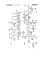
- FIG. 1 is a circuit diagram of a novel four-bit segmented dual gate field effect transistor (SDGFET Transistor) with power control circuitry, the configuration forming a power cell in a monolithic microwave integrated circuit (MMIC) power amplifier which maintains high power added efficiency while reducing power in 16 digital steps;
- SDGFET Transistor segmented dual gate field effect transistor
- MMIC monolithic microwave integrated circuit
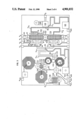
- FIG. 2 is a circuit diagram of the complete MMIC amplifier utilizing the power cell of FIG. 1, and providing additional means for efficiently substituting amplifiers of scaled power levels;
- FIG. 3 is a layout of the MMIC amplifier illustrated in FIG. 2;
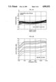
- FIGS. 4A, 4B and 4C are three curves illustrating the performance of a two stage 3 bit SDGFET amplifier; FIG. 4A illustrating the constancy of the incidental phase shift as the power is reduced; FIG. 4B illustrating the constancy of power with frequency over a range of selected power reductions; and FIG. 4C illustrating the much higher normalized power added efficiency vs power output of the exemplary SDGFET transistor amplifier in comparison to a linear amplifier as the power is reduced; and
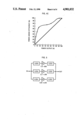
- FIG. 5 is a simplified block diagram of a power amplifier combination in which three SDGFET power amplifiers of successively lower powers are connected in parallel for successive substitution, and in which high power added efficiency is maintained as the power level is reduced.
- FIG. 1 is a circuit diagram of a four bit segmented dual gate field effect transistor (SDGFET Transistor) and power control circuit, forming a power cell in a monolithic microwave integrated circuit (MMIC) and providing an efficient digitally stepped power source.
- SDGFET Transistor dual gate field effect transistor
- MMIC monolithic microwave integrated circuit
- the circuit diagram is generic to power cells which may be scaled down in power from watts to milliwatts while maintaining high power added efficiency. Should one desire to cover the full range of a thousand to one, one might require three such power cells; one for covering a lower range (e.g. from ten to one hundred milliwatts), another for covering a middle range (e.g. from one hundred milliwatts to a watt), and a third for covering an upper range (e.g. from one watt to ten watts). This selection is approximate and exemplary. The range that an individual power cell may be required to cover, will depend upon the performance criteria, and thus might involve smaller or larger numbers of power cells.
- SDGFET Transistor single segmented dual gate field effect transistor
- the three signal connections are as in a single transistor; a common source electrode connected to signal ground, a common first gate electrode connected to the signal input, and a common drain electrode connected to the signal output. No signal connections are made to the number two gate electrode, which is segmented, and which activates coextensive segmented regions of the arrangement.
- the circuit diagram of FIG. 1 is not an amplifier since it omits the signal conditioning, filtering and signal loads in the energization paths required of a complete amplifier.
- the device is most appropriately characterized as a variable geometry FET transistor.
- the control circuitry illustrated in FIG. 1 connected to pads P A , P B , P C , and P D and leading to the segmented number two gate electrode activate selected segments of the FET to adjust the power level, thus making the device functionally a variable geometry FET transistor.
- the illustrated transistor device is a segmented dual gate FET of eight segments T1, T2, . . . T8.
- a set of segments (1 to 4) of the number two gate electrodes are activated, then a virtual transistor is formed having segmental dimensions corresponding to the activated segment.
- Each set of number two gate electrode segments activates coextensive portions of the source electrode, coextensive portions of the signal gate electrode, and coextensive portions of the drain electrode.
- the segment control network comprises four rf filter networks, the latter comprising both series connected resistors R1 to R4 and by-pass capacitors C1 to C4.
- the relative phase shifts of the SDGFET transistors between states is minimized by selection of the capacitors C 1 to C 4 , which are scaled in direct proportion to the widths of the FET segments and the resistors R 1 to R 4 which are scaled in inverse proportion to the widths of the segments.
- the resistors are also selected to prevent self biasing action under power conditions. The reduction is proportioned to allow the control voltage to sink/source the fractions of a milliampere of gate current required to maintain gate control.
- the segment control network links the second gate electrodes of eight segments to four separate conduction control terminals (P A , P B , P C , and P D ) providing a selection of 2 4 (i.e. 16) segment configurations corresponding to 2 4 power states.
- the electrical connections to the 16 state power cell are illustrated in FIG. 1.
- the eight segments are individually legended T1, T2, ...T8.
- the source electrode of each segment is a portion of a continuous electrode and is connected to ground.
- the first or signal gate electrode of each segment is also a portion of a continuous electrode, and is connected to the node N I (I for input).
- the second or control gate is segmented, as will be explained below, and connected to the segment control network.
- the drain electrode of each segment is a portion of a continuous electrode and is connected to the node N O (O for output).
- the segmented second gates of the FET segments are connected as follows to the segment control network.
- the second gate of the segment T 1 is connected to the junction of R 1 and C 1 and via R 1 to the segment control pad P D .
- the second gate of the segment T 2 is connected to the junction of R 2 and C 2 , and via R 2 to the segment control pad P C .
- the second gates of the third and fourth segments T 3 and T 4 are connected to the junction of R 3 and C 3 , and via R 3 to the segment control pad P B .
- the second gates of the segment T 5 , T 6 , T 7 and T 8 are connected to the junction of R 4 and C 4 , and via R 4 to the segment control pad P A .
- the FIG. 1 power cell is adjusted for efficient operation at the maximum power level, and for a minimum reduction in power efficiency as the power level is decreased.
- the FET segments are of a common gate length and of effectively binary scaled gate widths.
- the effective gate widths and circuit values of the segment control circuits for a 10 GHz application are illustrated in FIG. 1.
- the SDGFET transistor is MMIC fabricated, formed as part of the larger amplifier circuit illustrated in FIG. 2, using the layout shown in FIG. 3.
- the substrate is fabricated upon a 5 mil gallium arsenide substrate.
- the selection of gallium arsenide as the substrate material is in accordance with current practice for field effect transistors designed to work in the range of from one to 100 Gigahertz.
- the electrodes of the eight segments may be sections of a continuous electrode structure, with segmentation of the number two gate electrode permitting coextensive regions of the source electrode and drain electrode to become active while adjacent regions remain inactive as earlier explained.
- segmentation of the number two gate electrodes defines segmental regions of the FETs without the need to partition the source, signal gate, or drain electrodes.
- the segments of control gates may be either formed of unequal length segments scaled in a binary fashion or formed of equal length segments with the segments being conductively connected in sets of 1, 2, or 4 to achieve binary scaling.
- the binary scaling of segments results in a linear power scale, i.e., for a 4-bit device, the relative power is adjustable from 16/16 to 1/16 in 1/16 steps. This adjustment range is thus denser at maximum power, and coarser with steeper steps at lower powers.
- This type of scale is desirable from a phased array viewpoint since sum pattern weights, such as Taylor weights, exhibit fine, small steps near the center with a gentle roll-off that becomes increasingly more rapid as the edge is approached.
- a linear scale as is implemented in the described embodiment will thus result in lower sidelobes than a dB scale due to better quantization fidelity of the desired pattern weights.
- the smallest segment (T 1 ) is one-half the width of the other segments (T 2 -T 8 ), which while being equal in width are connected together in sets of 1, 2, or 4.
- good rf signal manifolding may dictate a parallel row structure, in which the length of a row or half or one-quarter of a row corresponds to the lowest digital value, and two or four rows are manifolded to form the widest segments.
- the power state of the SDGFET transistor of FIG. 1 is controlled by the applied DC voltages.
- the source electrode (common to all segments) is connected to substrate ground and the voltages applied to the other electrodes are referenced to substrate ground.
- the drain voltage (V DS ) coupled to the common drain electrode is typically 10 volts for the maximum power setting.
- Maximum power operation results when the number one or signal grid (common to all segments) is at a maximum power setting (V GS ), typically at minus one volt.
- V GS maximum power setting
- the rf signal is set for saturated class "A" operation, (i.e. with conduction occurring throughout the rf cycle).
- For maximum power of the SDGFET transistors typically zero control voltages are applied via the pads P A , P B , P C , P D , to the number two gate electrodes.
- the power in accordance with the invention, may be digitally reduced while maintaining efficiency, by switching off individual segments by application of a pinch-off voltage (V P ) to the number two gate electrodes.
- V P a pinch-off voltage
- the pinch-off voltage is typically minus 3.5 volts. Zero power occurs when all the number two gate electrodes are at pinch-off voltage.
- a third state of the SDGFET transistor is a high conduction low-power state using zero bias drain switching. This state is used when the amplifier is inactive and it is desired to isolate the inactive amplifier from parallelled active amplifiers.
- a depletion mode SDGFET transistor with the drain voltage removed and a zero gate or near zero gate potential applied to the number two gate electrode, reverts to a low impedance state in which the resistance between source and drain is very low, typically from 0.2 to one ohm. This feature is useful when quarter wave isolation paths are provided to convert the low impedance short circuit in the signal path to a high impedance open circuit at operating frequencies at the circuit branches. With inactive amplifiers appearing to be open circuits, parallel connection of active and inactive amplifiers is permitted without the loss of efficiency caused by loading due to the inactive amplifier.
- the SDGFET transistor In normal operation, the SDGFET transistor is operated with an ac signal on the number one gate electrode having a maximum value set by allowable distortion and one that is insufficient to cut-off the segment on negative signal swings when biased for maximum efficient power. Successively lower power states are then achieved by applying a pinch-off potential via the pads P A , P B , P C , and P D to the number two gate electrodes to achieve lower power states with sustained power added efficiency.
- the SDGFET transistor is preferably operated in saturation for efficiency, as noted earlier.
- saturated operation has the advantage of leveling the output signal against variations in the input signal.
- sufficient signal drive is required of a driver stage to insure that there is adequate gain to drive the SDGFET into saturation in the lowest power states.
- adequate gain for the lowest power state results in several (e.g. 6 or 7) db of overdrive in the highest power state.
- Moderate overdrive due to the signal equalizing effect of saturated operation, does not adversely affect the accuracy of the desired power levels and ordinarily harmonic distortion is of minor concern and readily removed if desired.
- the amplifier circuit for an intermediate power range of from 100 milliwatts to a watt is illustrated in FIG. 2, with the layout of a MMIC embodiment being illustrated in FIG. 3.
- the amplifier provides an input switch for amplifier isolation when paralleled and a driver stage for the power amplifier insuring saturated operation.
- the power amplifier employs two SDGFET transistors.
- the amplifier is accordingly designed to being paralleled with two other like amplifiers having a respectively lower and higher power range without loss in power added efficiency.
- the signal input pad P I is connected to a shunt connected transistor switch T 10 .
- the drain electrode of the transistor switch is connected to the pad P I and the source electrode is connected to ground, with the gate electrode being connected via a 50 ohm resistor R 10 to the pad P CTL .
- Control potentials are applied to the control potential pad P CTL to operate the switch.
- the switch is non-conductive by application of a negative bias to the gate, the shunt path is of near infinite resistance and signals may enter the amplifier.
- the switch is conductive by application of a zero or small positive bias, a low impedance short circuit occurs across the input, and signals are blocked from entering the amplifier.
- Input signals coupled to the input pad P I are fed through a tuned coupling network consisting of a serially connected inductor L 1 and a 1.25 pf capacitor C 10 to the gate electrode of driver transistor T 11 .
- the source of the transistor T 11 is grounded, and the gate electrode is connected via an rf filter consisting of a series 100 ohm resistor and a shunt 10 pf by-pass capacitor C 11 to the pad P VGI .
- the drain electrode of the preamplifier transistor is connected via a further rf filter (and load) inductor L 2 to the pad P VD , by-passed to ground by a 15 pf capacitor C 12 .
- the gain of the driver may be adjusted by the voltage applied to the pad P VG2 .
- Amplified signals appearing at the drain of T 11 are then coupled through an interstage coupling network to the node N 3 at the input to an impedance matching microstrip transmission line (TL 1 -TL 4 ) leading to the inputs of two paralleled SDGFET amplifiers.
- the interstage coupling network comprises series capacitor C 13 , shunt capacitor C 14 , series inductor L 3 , series 4.7 pf capacitor C 15 , shunt inductor L 4 , series 2.2 pf capacitor C 16 , and shunt 4.7 pf capacitor C 17 .
- the impedance matching network consists of a first transmission line TL 1 connected between node N 3 and node N 4 .
- the second transmission line TL 2 connects node N 4 via an rf filter consisting of a shunt capacitor C 18 and a series resistor R 12 to the pad P VG2 .
- the transmission line TL 3 connects the node N 4 to the number one gate electrode of the upper SDGFET transistor T 12 .
- the transmission line TL 4 connects the node N 4 to the number one gate electrode of the lower SDGFET transistor T 13 , thus closing the signal path from the output of the driver amplifier transmitter T 11 to the inputs of the two SDGFET transistors of the amplifier.
- the segmented transistors depicted in the blocks T 12 and T 13 of FIG. 2, and the control network have the circuit diagram illustrated in FIG. 1.
- the layout of the transistors (and the amplifier) are illustrated in FIG. 3. Since the two transistors T 12 and T 13 are identical, the description directed primarily to transistor T 12 also applies to transistor T 13 .
- the transistor segments indicated in FIG. 1 are enumerated as "rows" connected to the number one signal gate manifold G 12 to the left of the transistor and connected to transmission line TL 3 with the upper most row corresponding to the first segment T 1 , successively lower rows corresponding to T 2 , T 3 , etc. to T 8 .
- the number two control gate of transistor segment T 1 is connected via the filter R 1 , C 1 to the upper pad P D .
- the number two control gate of transistor segment T 2 is connected via the filter R 2 , C 2 to the upper pad P C .
- the number two gates of transistor segments T 3 and T 4 are connected via the filter R 3 , C 3 to the upper pad P B .
- the number two gates of transistor segments T 5 -T 8 are connected via the filter R 4 , C 4 to the upper pad P A .
- the outputs from the drain manifolds of T 12 and T 13 are connected by two balanced transmission lines TL 5 and TL 6 to the node N 5 .
- the drain node T 5 is returned via the transmission line TL 7 , by-passed by capacitor C 21 to the pad P VD for application of drain potentials.
- the drain node N 5 is coupled by a capacitive impedance transformer C 19 , C 20 to the output pad P 0 .
- the input transmission lines TL 3 and TL 4 and output transmission lines TL 5 and TL 6 are designed to provide balanced input signal distribution to the signal gates and balanced output signal derivation from the two transistors T 12 and T 13 .
- the resistor R 13 interconnects the number one signal gate manifolds of transistors T 12 and T 13
- the resistor R 14 interconnects the drain manifolds of transistors T 12 and T 13 .
- the signal power output from transistors and dc power supplied to the output SDGFETs T 12 and T 13 is coupled to node N 5 .
- the output signal is coupled from node N 5 via a capacitive voltage divider C 19 and C 20 to the signal output pat P 0 .
- DC power is supplied to the node N 5 from the pad P VD2 , through an rf filter comprising the by-pass capacitor C 21 and the transmission line element TL 7 .
- FIGS. 4A, 4B and 4C An arrangement similar to that illustrated in FIG. 1 but having 2 6 or 64 states, achieved by cascading two stages each having 8 states provides the performance illustrated in FIGS. 4A, 4B and 4C.
- the arrangement maintains a phase transfer performance to within plus or minus 5° over a band of 7 to 11 Gigahertz, and over a dynamic range of 20 dB (100-1 in voltage).
- FIG. 4B The power output of the 64 state arrangement over approximately the same frequency range (6.75 to 11.25 Gigahertz) is illustrated in FIG. 4B.
- the individual plots illustrate a substantially flat (plus or minus 2 dB) power level from 7.65 to 11.25 Gigahertz over a 15 dB dynamic range (i.e. 500 mw to 10 mw).
- FIG. 4C illustrates the normalized power added efficiency versus power output of the same 6 bit arrangement. The curve illustrates that at a power reduction to about 15%, the normalized power added efficiency of the arrangement remains above 65%, before it drops precipitously due to a reduction in gain. In comparison, the power added efficiency of a conventional linear amplifier falls linearly so that at a power reduction to 15%, the normalized power added efficiency is reduced to 15%, or four times worse.
- the cascade of two SDGFET states results in a wider power adjustment range equal to the sum of the individual stage range on a dB scale, but at the expense of operation in the low efficiency region (below 20%) shown on FIG. 4C.
- the linear preamplification stage in the former allows specification of gain level independent of power adjustment range.
- an embodiment with constant input power utilizing paralleled SDGFET power amplifier stages requires preamplification in the higher power stages.
- the invention permits one to retain a normalized efficiency in excess of 65%, if one is content not to reduce the power further than to 15% of the maximum in the exemplary design. Granted that a greater range of efficient power reduction is required, and that one must satisfy power added efficiency, transmit gain and a maximum transmit drain level, and at the same time minimize GaAs chip size, one may parallel several amplifiers in the manner illustrated in FIG. 5.
- three amplifiers each having overlapping power levels approximately ten times greater than the succeeding one, and each having an approximately 10 to 1 range of power levels (or 4 bits) may be efficiently paralleled to achieve a 30 dB range of efficient power levels. While one could use a single amplifier with additional bits of power resolution, a constrained conservative design dictates that one use 4 bits of each of three 5 bit SDGFET transistors, in three paralleled amplifiers to achieve the desired power control range.
- the fifth bit is for calibration purposes, i.e., to maintain uniform power step size, particularly at crossovers between parallel paths.
- the three-way branching avoids the loss in signal gain as the number of active segments are being reduced in a SDGFET transistor.
- all portions of the number one signal gates are driven, which sustains the input loading and phase response but reduces the signal gain.
- Assuming a 16 to 1 power reduction only 6.25% of the signal drive is used to drive the active segment in the lowest power setting and 93.75% of the signal is unused.
- the resultant gain reduction can be mitigated by cascading two segmented stages so as to provide increased drive at higher power levels, and reducing the scaling ratios in both the driver and power stages.
- three bits of gain reduction are provided in each stage to achieve 64 bits of power adjustment. The strategy significantly improves the power added efficiency at lower power levels over that of a non-segmented design.
- a strategy which is more efficient of signal energy is that provided by paralleling segmented but isolatable power amplifiers of scaled power levels as for instance in three parallel branches. Branching allows each amplifier to be segmented for a more limited range of power reduction, but the circuit for isolating the inactive amplifiers must insure that, while connected in parallel, the inactive amplifier does not absorb signal energy.
- each power amplifier has a low impedance switch at the amplifier input spaced a quarter wavelength from an input node common to the three amplifiers.
- each power amplifier has an amplifier output stage, (when it has a low impedance zero drain bias off state), or an independent switch at the amplifier output spaced a quarter wavelength from the common output node.
- each inactive amplifier exhibits an input and an output short circuit impedance at the center of the operating band, and that each short circuit is spaced by a quarter wave path to the respective common input and output nodes, each will appear to be an open circuit at the nearest node.
- no input signal energy will be diverted to the inactive amplifier from the source of input signals nor will output signal energy be diverted from the active amplifier to the inactive amplifier.
- the transistor T 10 is an input switch, which may become a low impedance short circuit by applying a zero or small positive voltage via the pad P CTL to the gate electrode. A grounded source without the need for a drain potential is all that is required.
- the switch T 10 may be turned off by applying the negative pinch-off potential to the gate electrode. In the conductive state, the switch T 10 neither absorbs energy from the power supply nor significant energy from the signal.
- the output stages of the inactive power amplifiers are non-dissipative of the signal at the output node N 5 .
- each output stage is adjusted for a low impedance state by using zero bias drain switching which is of a sufficiently low value as to achieve the desired reflection.
- a shunt switch is provided at the amplifier output and a suitable bias is applied to the gate electrode of the switch (with zero drain voltage) to achieve the desired low impedance state.
- the gate switched FET shunt switches and the zero bias drain switched SDGFET transistors operate efficiently.
- the devices are in the low impedance state (when the amplifiers are inactive), neither absorbs energy from the drain bias supply nor significant signal energy. This permits one to parallel amplifiers containing SDGFET transistors without loss in power efficiency as the power level is reduced, should conservative design for yield enhancement, gain considerations, or chip size, (etc.) dictate a paralleled design.
- the selection of SDGFET power amplifier topology is based upon maintaining efficiency. If the SDGFET device is increased in width by adding additional fingers, at some point, efficiency will degrade due to phase lag upon gate and drain manifolds preventing coherent summation of the power contribution of each segment. Similarly, if finger length is increased too far, gate and drain attenuation of the power contribution will degrade efficiency.
- the multiple SDGFET cell approach as depicted in FIGS. 2 and 3 is the selection of choice, when further power adjustment range than is efficiently attainable in a single amplifier is required, the parallel approach is the selection. For the example of FIG. 5, each parallel amplifier stage results in a range extension of 10 dB.
- the granularity i.e, resolution or number of bits
- the granularity is determined by the number of bits in each SDGFET amplifier, while the range is determined by the number of parallel amplifier stages. For the example given with 4-bit resolution per amplifier, the composite result is 51/2-bit resolution over a 30 dB range. If a fourth path is added, 6-bit resolution over a 40 dB range is realizable, i.e., each binary increment in parallel paths results in an increase of resolution by one bit.
- the invention has primary application to radio frequency amplifiers in radar transmitters in phased array radar systems.
- the frequencies of interest are now often in excess of 1 GHZ, and approaching 100 GHZ.
- the SDGFET power transistors are normally formed using high frequency semiconductor materials such as GaAs.
- GaAs materials are employed, and the frequencies are sufficiently high to permit compact electronic circuit layouts, the SDGFET transistors and associated circuits making up the complete amplifier may be fabricated on a single substrate using monolithic microwave integrated circuit (MMIC) techniques.
- MMIC monolithic microwave integrated circuit
- the invention may, of course, be applied to r.f. power systems, other than phased array radar systems, and may be carried out using discrete transistors in hybrid arrangements, and using other lower frequency semiconductor materials.
Abstract
Description
Claims (5)
Priority Applications (1)
| Application Number | Priority Date | Filing Date | Title |
|---|---|---|---|
| US07/278,548 US4901032A (en) | 1988-12-01 | 1988-12-01 | Digitally controlled variable power amplifier |
Applications Claiming Priority (1)
| Application Number | Priority Date | Filing Date | Title |
|---|---|---|---|
| US07/278,548 US4901032A (en) | 1988-12-01 | 1988-12-01 | Digitally controlled variable power amplifier |
Publications (1)
| Publication Number | Publication Date |
|---|---|
| US4901032A true US4901032A (en) | 1990-02-13 |
Family
ID=23065423
Family Applications (1)
| Application Number | Title | Priority Date | Filing Date |
|---|---|---|---|
| US07/278,548 Expired - Fee Related US4901032A (en) | 1988-12-01 | 1988-12-01 | Digitally controlled variable power amplifier |
Country Status (1)
| Country | Link |
|---|---|
| US (1) | US4901032A (en) |
Cited By (39)
| Publication number | Priority date | Publication date | Assignee | Title |
|---|---|---|---|---|
| US4947136A (en) * | 1989-09-18 | 1990-08-07 | General Electric Company | Variable gain distributed amplifier |
| US5060294A (en) * | 1990-07-05 | 1991-10-22 | Motorola, Inc. | Dual mode power amplifier for radiotelephone |
| US5103233A (en) * | 1991-04-16 | 1992-04-07 | General Electric Co. | Radar system with elevation-responsive PRF control, beam multiplex control, and pulse integration control responsive to azimuth angle |
| US5115244A (en) * | 1991-04-16 | 1992-05-19 | General Electric Company | Radar system with active array antenna, elevation-responsive PRF control, and pulse integration control responsive to azimuth angle |
| US5115243A (en) * | 1991-04-16 | 1992-05-19 | General Electric Co. | Radar system with active array antenna, beam multiplex control and pulse integration control responsive to azimuth angle |
| US5128683A (en) * | 1991-04-16 | 1992-07-07 | General Electric Company | Radar system with active array antenna, elevation-responsive PRF control, and beam multiplex control |
| US5361403A (en) * | 1990-11-14 | 1994-11-01 | Ericsson Ge Mobile Communication Holding, Inc. | AM-FM transmitter power amplifier |
| US5408198A (en) * | 1993-04-27 | 1995-04-18 | Sony Corporation | Semiconductor power amplifier integrated circuit |
| US5432473A (en) * | 1993-07-14 | 1995-07-11 | Nokia Mobile Phones, Limited | Dual mode amplifier with bias control |
| US5493255A (en) * | 1995-03-21 | 1996-02-20 | Nokia Mobile Phones Ltd. | Bias control circuit for an RF power amplifier |
| EP0687060A3 (en) * | 1994-06-09 | 1997-11-26 | Mitsubishi Denki Kabushiki Kaisha | Power amplifier |
| US5872481A (en) * | 1995-12-27 | 1999-02-16 | Qualcomm Incorporated | Efficient parallel-stage power amplifier |
| US5974041A (en) * | 1995-12-27 | 1999-10-26 | Qualcomm Incorporated | Efficient parallel-stage power amplifier |
| US6069525A (en) * | 1997-04-17 | 2000-05-30 | Qualcomm Incorporated | Dual-mode amplifier with high efficiency and high linearity |
| US6069526A (en) * | 1998-08-04 | 2000-05-30 | Qualcomm Incorporated | Partial or complete amplifier bypass |
| WO2000045508A1 (en) * | 1999-01-27 | 2000-08-03 | Qinetiq Limited | Microwave amplifiers |
| US6232840B1 (en) * | 1999-06-10 | 2001-05-15 | Raytheon Company | Transistor amplifier having reduced parasitic oscillations |
| US6265944B1 (en) * | 1999-09-27 | 2001-07-24 | Conexant Systems, Inc. | Fully integrated broadband RF voltage amplifier with enhanced voltage gain and method |
| EP1168604A1 (en) * | 2000-02-08 | 2002-01-02 | Mitsubishi Denki Kabushiki Kaisha | Multistage amplifier |
| US20030107362A1 (en) * | 2001-12-07 | 2003-06-12 | Kohei Oikawa | Voltage generator circuit for use in a semiconductor device |
| US6621374B2 (en) * | 2001-07-19 | 2003-09-16 | Lockheed Martin Corporation | Splitter/combiner using artificial transmission lines, and paralleled amplifier using same |
| US20040140851A1 (en) * | 2003-01-17 | 2004-07-22 | M/A Com, Inc. | Apparatus, methods and articles of manufacture for control in an electromagnetic processor |
| EP1672781A1 (en) * | 2004-12-16 | 2006-06-21 | M/A-Com, Inc. | Method and apparatus for compensating amplifier output for temperature and process variations |
| US20060226902A1 (en) * | 2005-04-12 | 2006-10-12 | White Mikel J | Amplifying a signal using a current shared power amplifier |
| US20070152751A1 (en) * | 2005-12-21 | 2007-07-05 | Trex Enterprises Corp. | Wide bandwidth, high power amplifier |
| US20090309661A1 (en) * | 2008-06-13 | 2009-12-17 | Jaejoon Chang | Systems and Methods for Switching Mode Power Amplifier Control |
| US20100053470A1 (en) * | 2006-12-05 | 2010-03-04 | Thomson Licensing | Active distributed signal splitting apparatus |
| EP2230762A3 (en) * | 2006-12-05 | 2010-12-29 | Thomson Licensing | Active distributed signal splitting apparatus |
| US20110037516A1 (en) * | 2009-08-03 | 2011-02-17 | Qualcomm Incorporated | Multi-stage impedance matching |
| US20130057428A1 (en) * | 2010-03-08 | 2013-03-07 | Armin Himmelstoss | Radar sensor and method for controlling same to reduce the crosstalk of digital signals to the hf radar signal |
| US8461921B2 (en) | 2009-08-04 | 2013-06-11 | Qualcomm, Incorporated | Amplifier module with multiple operating modes |
| US20130314163A1 (en) * | 2012-05-22 | 2013-11-28 | Rf Micro Devices, Inc. | Integrated stacked power amplifier and rf switch architecture |
| US8723602B2 (en) * | 2012-08-10 | 2014-05-13 | Tensorcom, Inc. | Method and apparatus for a class-E load tuned beamforming 60 GHz transmitter |
| US8873339B2 (en) | 2012-08-10 | 2014-10-28 | Tensorcom, Inc. | Method and apparatus for a clock and signal distribution network for a 60 GHz transmitter system |
| US9007124B1 (en) | 2012-09-17 | 2015-04-14 | Bae Systems Information And Electronic Systems Integration Inc. | Tile array PA module using quadrature balanced PA MMICs |
| US9065391B1 (en) | 2012-09-17 | 2015-06-23 | Bae Systems Information And Electronic Systems Integration Inc. | Method of operating a power amplifier in class F/inverse class F |
| US9118284B1 (en) | 2012-09-17 | 2015-08-25 | Bae Systems Information And Electronic Systems Integration Inc. | Cascode power amplifier |
| WO2016018527A1 (en) * | 2014-07-30 | 2016-02-04 | Eridan Communications, Inc. | Limiting driver for switch-mode power amplifier |
| US11018425B1 (en) * | 2015-05-01 | 2021-05-25 | Rockwell Collins, Inc. | Active electronically scanned array with power amplifier drain bias tapering for optimal power added efficiency |
Citations (3)
| Publication number | Priority date | Publication date | Assignee | Title |
|---|---|---|---|---|
| US4598252A (en) * | 1984-07-06 | 1986-07-01 | Itt Corporation | Variable gain power amplifier |
| US4638190A (en) * | 1985-05-20 | 1987-01-20 | General Electric Company | Digitally controlled wideband phase shifter |
| US4734751A (en) * | 1985-05-20 | 1988-03-29 | General Electric Company | Signal scaling MESFET of a segmented dual gate design |
-
1988
- 1988-12-01 US US07/278,548 patent/US4901032A/en not_active Expired - Fee Related
Patent Citations (3)
| Publication number | Priority date | Publication date | Assignee | Title |
|---|---|---|---|---|
| US4598252A (en) * | 1984-07-06 | 1986-07-01 | Itt Corporation | Variable gain power amplifier |
| US4638190A (en) * | 1985-05-20 | 1987-01-20 | General Electric Company | Digitally controlled wideband phase shifter |
| US4734751A (en) * | 1985-05-20 | 1988-03-29 | General Electric Company | Signal scaling MESFET of a segmented dual gate design |
Cited By (55)
| Publication number | Priority date | Publication date | Assignee | Title |
|---|---|---|---|---|
| US4947136A (en) * | 1989-09-18 | 1990-08-07 | General Electric Company | Variable gain distributed amplifier |
| US5060294A (en) * | 1990-07-05 | 1991-10-22 | Motorola, Inc. | Dual mode power amplifier for radiotelephone |
| US5361403A (en) * | 1990-11-14 | 1994-11-01 | Ericsson Ge Mobile Communication Holding, Inc. | AM-FM transmitter power amplifier |
| US5423074A (en) * | 1990-11-14 | 1995-06-06 | Ericsson Ge Mobile Communications Inc. | AM-FM transmitter power amplifier |
| EP0509843A2 (en) * | 1991-04-16 | 1992-10-21 | General Electric Company | Radar system with active array antenna, elevation-responsive PRF control, and beam multiplex control |
| US5128683A (en) * | 1991-04-16 | 1992-07-07 | General Electric Company | Radar system with active array antenna, elevation-responsive PRF control, and beam multiplex control |
| EP0509843A3 (en) * | 1991-04-16 | 1993-05-12 | General Electric Company | Radar system with active array antenna, elevation-responsive prf control, and beam multiplex control |
| US5115243A (en) * | 1991-04-16 | 1992-05-19 | General Electric Co. | Radar system with active array antenna, beam multiplex control and pulse integration control responsive to azimuth angle |
| US5115244A (en) * | 1991-04-16 | 1992-05-19 | General Electric Company | Radar system with active array antenna, elevation-responsive PRF control, and pulse integration control responsive to azimuth angle |
| US5103233A (en) * | 1991-04-16 | 1992-04-07 | General Electric Co. | Radar system with elevation-responsive PRF control, beam multiplex control, and pulse integration control responsive to azimuth angle |
| US5408198A (en) * | 1993-04-27 | 1995-04-18 | Sony Corporation | Semiconductor power amplifier integrated circuit |
| US5432473A (en) * | 1993-07-14 | 1995-07-11 | Nokia Mobile Phones, Limited | Dual mode amplifier with bias control |
| EP0687060A3 (en) * | 1994-06-09 | 1997-11-26 | Mitsubishi Denki Kabushiki Kaisha | Power amplifier |
| US5493255A (en) * | 1995-03-21 | 1996-02-20 | Nokia Mobile Phones Ltd. | Bias control circuit for an RF power amplifier |
| US5872481A (en) * | 1995-12-27 | 1999-02-16 | Qualcomm Incorporated | Efficient parallel-stage power amplifier |
| US5974041A (en) * | 1995-12-27 | 1999-10-26 | Qualcomm Incorporated | Efficient parallel-stage power amplifier |
| US6069525A (en) * | 1997-04-17 | 2000-05-30 | Qualcomm Incorporated | Dual-mode amplifier with high efficiency and high linearity |
| US6069526A (en) * | 1998-08-04 | 2000-05-30 | Qualcomm Incorporated | Partial or complete amplifier bypass |
| WO2000045508A1 (en) * | 1999-01-27 | 2000-08-03 | Qinetiq Limited | Microwave amplifiers |
| US6232840B1 (en) * | 1999-06-10 | 2001-05-15 | Raytheon Company | Transistor amplifier having reduced parasitic oscillations |
| US6265944B1 (en) * | 1999-09-27 | 2001-07-24 | Conexant Systems, Inc. | Fully integrated broadband RF voltage amplifier with enhanced voltage gain and method |
| EP1168604A1 (en) * | 2000-02-08 | 2002-01-02 | Mitsubishi Denki Kabushiki Kaisha | Multistage amplifier |
| EP1168604A4 (en) * | 2000-02-08 | 2005-07-06 | Mitsubishi Electric Corp | Multistage amplifier |
| US6621374B2 (en) * | 2001-07-19 | 2003-09-16 | Lockheed Martin Corporation | Splitter/combiner using artificial transmission lines, and paralleled amplifier using same |
| US20030107362A1 (en) * | 2001-12-07 | 2003-06-12 | Kohei Oikawa | Voltage generator circuit for use in a semiconductor device |
| US6744302B2 (en) * | 2001-12-07 | 2004-06-01 | Kabushiki Kaisha Toshiba | Voltage generator circuit for use in a semiconductor device |
| WO2004068701A1 (en) * | 2003-01-17 | 2004-08-12 | M/A-Com, Inc. | Apparatus, methods and articles of manufacture for control in an electromagnetic processor |
| US20040140851A1 (en) * | 2003-01-17 | 2004-07-22 | M/A Com, Inc. | Apparatus, methods and articles of manufacture for control in an electromagnetic processor |
| US6859098B2 (en) | 2003-01-17 | 2005-02-22 | M/A-Com, Inc. | Apparatus, methods and articles of manufacture for control in an electromagnetic processor |
| EP1672781A1 (en) * | 2004-12-16 | 2006-06-21 | M/A-Com, Inc. | Method and apparatus for compensating amplifier output for temperature and process variations |
| US20060132230A1 (en) * | 2004-12-16 | 2006-06-22 | M/A-Com, Inc. | Method and apparatus for compensating amplifier output for temperature and process variations |
| US7154329B2 (en) | 2004-12-16 | 2006-12-26 | M/A-Com, Inc. | Method and apparatus for compensating amplifier output for temperature and process variations |
| US7256654B2 (en) | 2005-04-12 | 2007-08-14 | Raytheon Company | Amplifying a signal using a current shared power amplifier |
| US20060226902A1 (en) * | 2005-04-12 | 2006-10-12 | White Mikel J | Amplifying a signal using a current shared power amplifier |
| US7486141B2 (en) * | 2005-12-21 | 2009-02-03 | Trex Enterprises Corp. | Wide bandwidth, high power amplifier |
| US20070152751A1 (en) * | 2005-12-21 | 2007-07-05 | Trex Enterprises Corp. | Wide bandwidth, high power amplifier |
| US20100053470A1 (en) * | 2006-12-05 | 2010-03-04 | Thomson Licensing | Active distributed signal splitting apparatus |
| EP2230762A3 (en) * | 2006-12-05 | 2010-12-29 | Thomson Licensing | Active distributed signal splitting apparatus |
| US20090309661A1 (en) * | 2008-06-13 | 2009-12-17 | Jaejoon Chang | Systems and Methods for Switching Mode Power Amplifier Control |
| US7768353B2 (en) | 2008-06-13 | 2010-08-03 | Samsung Electro-Mechanics Company, Ltd. | Systems and methods for switching mode power amplifier control |
| US8536950B2 (en) | 2009-08-03 | 2013-09-17 | Qualcomm Incorporated | Multi-stage impedance matching |
| US20110037516A1 (en) * | 2009-08-03 | 2011-02-17 | Qualcomm Incorporated | Multi-stage impedance matching |
| US8461921B2 (en) | 2009-08-04 | 2013-06-11 | Qualcomm, Incorporated | Amplifier module with multiple operating modes |
| US20130057428A1 (en) * | 2010-03-08 | 2013-03-07 | Armin Himmelstoss | Radar sensor and method for controlling same to reduce the crosstalk of digital signals to the hf radar signal |
| US9285473B2 (en) * | 2010-03-08 | 2016-03-15 | Robert Bosch Gmbh | Radar sensor and method for controlling same to reduce the crosstalk of digital signals to the HF radar signal |
| US20130314163A1 (en) * | 2012-05-22 | 2013-11-28 | Rf Micro Devices, Inc. | Integrated stacked power amplifier and rf switch architecture |
| US9019010B2 (en) * | 2012-05-22 | 2015-04-28 | Rf Micro Devices, Inc. | Integrated stacked power amplifier and RF switch architecture |
| US8723602B2 (en) * | 2012-08-10 | 2014-05-13 | Tensorcom, Inc. | Method and apparatus for a class-E load tuned beamforming 60 GHz transmitter |
| US8873339B2 (en) | 2012-08-10 | 2014-10-28 | Tensorcom, Inc. | Method and apparatus for a clock and signal distribution network for a 60 GHz transmitter system |
| US9007124B1 (en) | 2012-09-17 | 2015-04-14 | Bae Systems Information And Electronic Systems Integration Inc. | Tile array PA module using quadrature balanced PA MMICs |
| US9065391B1 (en) | 2012-09-17 | 2015-06-23 | Bae Systems Information And Electronic Systems Integration Inc. | Method of operating a power amplifier in class F/inverse class F |
| US9118284B1 (en) | 2012-09-17 | 2015-08-25 | Bae Systems Information And Electronic Systems Integration Inc. | Cascode power amplifier |
| US9407210B2 (en) | 2012-09-17 | 2016-08-02 | Bae Systems Information And Electronic Systems Integration Inc. | Cascode power amplifier |
| WO2016018527A1 (en) * | 2014-07-30 | 2016-02-04 | Eridan Communications, Inc. | Limiting driver for switch-mode power amplifier |
| US11018425B1 (en) * | 2015-05-01 | 2021-05-25 | Rockwell Collins, Inc. | Active electronically scanned array with power amplifier drain bias tapering for optimal power added efficiency |
Similar Documents
| Publication | Publication Date | Title |
|---|---|---|
| US4901032A (en) | Digitally controlled variable power amplifier | |
| US4598252A (en) | Variable gain power amplifier | |
| US5523716A (en) | Microwave predistortion linearizer | |
| US4637073A (en) | Transmit/receive switch | |
| US6597242B2 (en) | Reconfigurable device for amplifying RF signals | |
| US5808527A (en) | Tunable microwave network using microelectromechanical switches | |
| US4994773A (en) | Digitally controlled monolithic active phase shifter apparatus having a cascode configuration | |
| US7508267B1 (en) | GaN based digital controlled broadband MMIC power amplifier | |
| US6075414A (en) | High frequency amplifier having a variable attenuator connected to the base of an amplifier FET | |
| US20090261900A1 (en) | Apparatus for Coupling at Least One of a Plurality of Amplified Input Signals to an Output Terminal Using a Directional Coupler | |
| US6130570A (en) | MESFET circuit utilizing only positive power supplies | |
| US5659267A (en) | High gain K-band power amplifier with unconditionally stable MMIC FET cells | |
| US20030132814A1 (en) | Circuit topology for attenuator and switch circuits | |
| US4853649A (en) | Distributed fet amplifier and bias voltage supply circuit therefor | |
| US4547745A (en) | Composite amplifier with divider/combiner | |
| US6989788B2 (en) | Antenna array having apparatus for producing time-delayed microwave signals using selectable time delay stages | |
| US5317290A (en) | MMIC (monolithic microwave integrated circuit) switchable bidirectional phase shift network | |
| US6265953B1 (en) | Apparatus and method for enhancing the isolation of an MMIC cross-point switch | |
| US6828873B2 (en) | Integrated high frequency circuit for affecting the amplitude of signals | |
| US5521560A (en) | Minimum phase shift microwave attenuator | |
| US4760350A (en) | Internally matched power amplifier | |
| US6657497B1 (en) | Asymmetric, voltage optimized, wideband common-gate bi-directional MMIC amplifier | |
| US5243301A (en) | Microwave power amplifiers | |
| US5150083A (en) | Digitally controlled monolithic switch matrix using selectable dual gate FET power dividers and combiners | |
| Lee et al. | An adaptively biased stacked power amplifier without output matching network in 90-nm CMOS |
Legal Events
| Date | Code | Title | Description |
|---|---|---|---|
| FEPP | Fee payment procedure |
Free format text: PAYOR NUMBER ASSIGNED (ORIGINAL EVENT CODE: ASPN); ENTITY STATUS OF PATENT OWNER: LARGE ENTITY |
|
| AS | Assignment |
Owner name: GENERAL ELECTRIC COMPANY, A NY CORP. Free format text: ASSIGNMENT OF ASSIGNORS INTEREST.;ASSIGNOR:KOMIAK, JAMES J.;REEL/FRAME:005002/0886 Effective date: 19881128 |
|
| FEPP | Fee payment procedure |
Free format text: PAYER NUMBER DE-ASSIGNED (ORIGINAL EVENT CODE: RMPN); ENTITY STATUS OF PATENT OWNER: LARGE ENTITY |
|
| FPAY | Fee payment |
Year of fee payment: 4 |
|
| AS | Assignment |
Owner name: MARTIN MARIETTA CORPORATION, MARYLAND Free format text: ASSIGNMENT OF ASSIGNORS INTEREST;ASSIGNOR:GENERAL ELECTRIC COMPANY;REEL/FRAME:007046/0736 Effective date: 19940322 |
|
| AS | Assignment |
Owner name: LOCKHEED MARTIN CORPORATION, MARYLAND Free format text: ASSIGNMENT OF ASSIGNORS INTEREST;ASSIGNOR:MARTIN MARIETTA CORPORATION;REEL/FRAME:008628/0518 Effective date: 19960128 |
|
| REMI | Maintenance fee reminder mailed | ||
| FP | Lapsed due to failure to pay maintenance fee |
Effective date: 19980218 |
|
| FEPP | Fee payment procedure |
Free format text: PETITION RELATED TO MAINTENANCE FEES FILED (ORIGINAL EVENT CODE: PMFP); ENTITY STATUS OF PATENT OWNER: LARGE ENTITY |
|
| FEPP | Fee payment procedure |
Free format text: PETITION RELATED TO MAINTENANCE FEES GRANTED (ORIGINAL EVENT CODE: PMFG); ENTITY STATUS OF PATENT OWNER: LARGE ENTITY |
|
| SULP | Surcharge for late payment | ||
| PRDP | Patent reinstated due to the acceptance of a late maintenance fee |
Effective date: 20000317 |
|
| FEPP | Fee payment procedure |
Free format text: PAYOR NUMBER ASSIGNED (ORIGINAL EVENT CODE: ASPN); ENTITY STATUS OF PATENT OWNER: LARGE ENTITY |
|
| REMI | Maintenance fee reminder mailed | ||
| LAPS | Lapse for failure to pay maintenance fees | ||
| STCH | Information on status: patent discontinuation |
Free format text: PATENT EXPIRED DUE TO NONPAYMENT OF MAINTENANCE FEES UNDER 37 CFR 1.362 |
|
| FP | Lapsed due to failure to pay maintenance fee |
Effective date: 20020213 |