JP4015118B2 - Semiconductor device - Google Patents
Semiconductor device Download PDFInfo
- Publication number
- JP4015118B2 JP4015118B2 JP2004012736A JP2004012736A JP4015118B2 JP 4015118 B2 JP4015118 B2 JP 4015118B2 JP 2004012736 A JP2004012736 A JP 2004012736A JP 2004012736 A JP2004012736 A JP 2004012736A JP 4015118 B2 JP4015118 B2 JP 4015118B2
- Authority
- JP
- Japan
- Prior art keywords
- lead
- semiconductor chip
- support
- semiconductor device
- leads
- Prior art date
- Legal status (The legal status is an assumption and is not a legal conclusion. Google has not performed a legal analysis and makes no representation as to the accuracy of the status listed.)
- Expired - Fee Related
Links
Images


Classifications
-
- H—ELECTRICITY
- H01—ELECTRIC ELEMENTS
- H01L—SEMICONDUCTOR DEVICES NOT COVERED BY CLASS H10
- H01L2224/00—Indexing scheme for arrangements for connecting or disconnecting semiconductor or solid-state bodies and methods related thereto as covered by H01L24/00
- H01L2224/01—Means for bonding being attached to, or being formed on, the surface to be connected, e.g. chip-to-package, die-attach, "first-level" interconnects; Manufacturing methods related thereto
- H01L2224/42—Wire connectors; Manufacturing methods related thereto
- H01L2224/47—Structure, shape, material or disposition of the wire connectors after the connecting process
- H01L2224/48—Structure, shape, material or disposition of the wire connectors after the connecting process of an individual wire connector
- H01L2224/4805—Shape
- H01L2224/4809—Loop shape
- H01L2224/48091—Arched
-
- H—ELECTRICITY
- H01—ELECTRIC ELEMENTS
- H01L—SEMICONDUCTOR DEVICES NOT COVERED BY CLASS H10
- H01L2224/00—Indexing scheme for arrangements for connecting or disconnecting semiconductor or solid-state bodies and methods related thereto as covered by H01L24/00
- H01L2224/01—Means for bonding being attached to, or being formed on, the surface to be connected, e.g. chip-to-package, die-attach, "first-level" interconnects; Manufacturing methods related thereto
- H01L2224/42—Wire connectors; Manufacturing methods related thereto
- H01L2224/47—Structure, shape, material or disposition of the wire connectors after the connecting process
- H01L2224/48—Structure, shape, material or disposition of the wire connectors after the connecting process of an individual wire connector
- H01L2224/481—Disposition
- H01L2224/48151—Connecting between a semiconductor or solid-state body and an item not being a semiconductor or solid-state body, e.g. chip-to-substrate, chip-to-passive
- H01L2224/48221—Connecting between a semiconductor or solid-state body and an item not being a semiconductor or solid-state body, e.g. chip-to-substrate, chip-to-passive the body and the item being stacked
- H01L2224/48245—Connecting between a semiconductor or solid-state body and an item not being a semiconductor or solid-state body, e.g. chip-to-substrate, chip-to-passive the body and the item being stacked the item being metallic
- H01L2224/48247—Connecting between a semiconductor or solid-state body and an item not being a semiconductor or solid-state body, e.g. chip-to-substrate, chip-to-passive the body and the item being stacked the item being metallic connecting the wire to a bond pad of the item
-
- H—ELECTRICITY
- H01—ELECTRIC ELEMENTS
- H01L—SEMICONDUCTOR DEVICES NOT COVERED BY CLASS H10
- H01L2224/00—Indexing scheme for arrangements for connecting or disconnecting semiconductor or solid-state bodies and methods related thereto as covered by H01L24/00
- H01L2224/73—Means for bonding being of different types provided for in two or more of groups H01L2224/10, H01L2224/18, H01L2224/26, H01L2224/34, H01L2224/42, H01L2224/50, H01L2224/63, H01L2224/71
- H01L2224/732—Location after the connecting process
- H01L2224/73251—Location after the connecting process on different surfaces
- H01L2224/73265—Layer and wire connectors
Description
本発明は、リードフレーム及び半導体装置に関し、特に、多リードのリードフレーム及び半導体装置に適用して有効な技術に関するものである。 The present invention relates to a lead frame and a semiconductor device, and more particularly to a technique effective when applied to a multi-lead lead frame and a semiconductor device.
LSI等の半導体装置は、集積度の向上に伴って、より複雑な回路が搭載されその機能も高度なものとなっている。このような高機能化によって、半導体装置にはより多くの外部端子が必要となり、このために半導体チップに設けられるパッド電極及び半導体装置の外部端子であるリードの数もそれに対応して増加することとなる。例えば、ロジック半導体装置では、外部端子の数は数百にも及んでいる。このような多リードの半導体装置としては、QFP(Quad Flat Package)型の半導体装置が知られている。このQFP型の半導体装置では、半導体チップを封止する封止体の四側面に夫々複数のリードを設けるために、多リード化に適しており、半導体装置を実装基板に実装する場合に、半導体装置周囲のスペースを有効に利用できるという利点がある。 Semiconductor devices such as LSIs are equipped with more complex circuits and advanced functions as the degree of integration increases. With such high functionality, the semiconductor device needs more external terminals, and for this reason, the number of pads that are provided on the semiconductor chip and leads that are external terminals of the semiconductor device are correspondingly increased. It becomes. For example, a logic semiconductor device has hundreds of external terminals. As such a multi-lead semiconductor device, a QFP (Quad Flat Package) type semiconductor device is known. In this QFP-type semiconductor device, a plurality of leads are provided on each of the four side surfaces of the sealing body that seals the semiconductor chip, which is suitable for multiple leads. When the semiconductor device is mounted on a mounting substrate, There is an advantage that the space around the apparatus can be used effectively.
このようなQFP型の半導体装置の組み立てにはリードフレームが用いられる(例えば、非特許文献1)。この文献のP155〜P164にはリードフレームが示されており、特にP157及びP159には具体的なパターンが示されている。 A lead frame is used to assemble such a QFP type semiconductor device (for example, Non-Patent Document 1). P155 to P164 in this document show lead frames, and in particular, P157 and P159 show specific patterns.
また、前記微細化によって半導体チップに形成される素子数が増加し、それらの素子がより高速に動作するために、半導体チップからの発熱も増大することとなる。この問題に対処するために放熱性を向上させた半導体装置が知られている(例えば、非特許文献2)。この文献のP200〜P203にはヒートスプレッダを設けた半導体装置が記載されている。この半導体装置では半導体チップにヒートスプレッダを取り付けることによって、半導体装置の放熱性を向上させている。 In addition, the number of elements formed on the semiconductor chip increases due to the miniaturization, and these elements operate at higher speed, so that heat generation from the semiconductor chip also increases. A semiconductor device with improved heat dissipation to cope with this problem is known (for example, Non-Patent Document 2). P200 to P203 of this document describe a semiconductor device provided with a heat spreader. In this semiconductor device, heat dissipation of the semiconductor device is improved by attaching a heat spreader to the semiconductor chip.
前記多リード化に対応するために、リードフレームでは、各リード間の間隔であるリードピッチ及びリードの幅寸法を小さくすることが求められている。 In order to cope with the increase in the number of leads, the lead frame is required to reduce the lead pitch, which is the distance between the leads, and the lead width.
また、同様に半導体チップには前記高機能化によって多くのパッド電極が設けられており、各パッド電極間の間隔であるパッドピッチも小さくなっている。一般に半導体チップのパッド電極のピッチは種々のものがあるが、ウエハ当たりのチップ取得数を向上させるために、チップサイズは小さいことが望ましく、このため各パッド電極間のピッチも一段と小さく設定される傾向にある。 Similarly, a large number of pad electrodes are provided in the semiconductor chip due to the high functionality, and the pad pitch, which is the interval between the pad electrodes, is also reduced. In general, there are various pitches of pad electrodes of a semiconductor chip. However, in order to improve the number of chips obtained per wafer, it is desirable that the chip size is small. For this reason, the pitch between the pad electrodes is set to be smaller. There is a tendency.
このような理由から、多リードと各パッド電極との間をAu等のワイヤを用いてボンディングする場合、間隔が小さくなったことにより、隣接するワイヤ相互が接触するショートが発生しやすくなるという問題がある。特に半導体チップのコーナー部分では、パッド電極にボンディングしたワイヤが、半導体チップに対して斜め方向にワイヤが伸びるために、パッドピッチが同一であってもワイヤ相互間の間隔が小さくなるので、その傾向が強くなる。 For this reason, when bonding between multiple leads and each pad electrode using a wire such as Au, a short-circuit where adjacent wires come into contact with each other easily occurs due to a decrease in the interval. There is. In particular, at the corner portion of the semiconductor chip, the wire bonded to the pad electrode extends in an oblique direction with respect to the semiconductor chip. Therefore, even if the pad pitch is the same, the distance between the wires becomes small, and this tendency Becomes stronger.
また、ワイヤボンディング後の樹脂モールドの際に、各リードの機械的強度の低下或はワイヤ間隔の減少によって、モールド樹脂の流動によりワイヤが変形するワイヤ流れが生じることがあり、この変形によりワイヤのショートが発生するという問題がある。 In addition, during resin molding after wire bonding, a wire flow may occur in which the wire deforms due to the flow of the mold resin due to a decrease in mechanical strength of each lead or a decrease in wire spacing. There is a problem that a short circuit occurs.
加えて、QFPでは、中央に搭載された半導体チップに近づくにつれてリードの配置領域が狭まってくる。このため、リードの加工精度の限界から、リードピッチを半導体チップのパッドピッチに対して充分に微細化できない場合には、リードの先端を半導体チップに近付けることができなくなるので、パッド電極とリードとをボンディングするワイヤを長くせざるを得ない。このようにワイヤを長くした場合には、前記ショート或はワイヤ流れの発生の確率が高くなる。 In addition, in QFP, the lead placement area is narrowed as the semiconductor chip mounted at the center is approached. For this reason, if the lead pitch cannot be sufficiently reduced with respect to the pad pitch of the semiconductor chip due to the limit of the processing accuracy of the lead, the tip of the lead cannot be brought close to the semiconductor chip. The wire for bonding must be lengthened. When the wire is lengthened in this way, the probability of occurrence of the short circuit or the wire flow increases.
また、このようなリードの微細化によって、各リードの機械的強度は低下するために、僅かな力により変形しやすくなり、このような変形によっても前記ショートが発生する。 In addition, since the mechanical strength of each lead is reduced due to such miniaturization of the lead, the lead is easily deformed by a slight force, and the short circuit also occurs due to such deformation.
本発明の目的は、多リードの半導体装置のショート或はワイヤ流れの発生を防止し、ボンディングを安定させることが可能な技術を提供することにある。 An object of the present invention is to provide a technique capable of preventing the occurrence of a short circuit or wire flow in a multi-lead semiconductor device and stabilizing the bonding.
本発明の他の目的は、多リードの半導体装置の放熱特性を向上させることが可能な技術を提供することにある。 Another object of the present invention is to provide a technique capable of improving the heat dissipation characteristics of a multi-lead semiconductor device.
本発明の前記ならびにその他の目的と新規な特徴は、本明細書の記述及び添付図面から明らかになるであろう。 The above and other objects and novel features of the present invention will be apparent from the description of this specification and the accompanying drawings.
本願において開示される発明のうち、代表的なものの概要を簡単に説明すれば下記の通りである。 Of the inventions disclosed in this application, the outline of typical ones will be briefly described as follows.
支持体に半導体チップを搭載し、この支持体に絶縁体を介してインナーリードを固定した半導体装置について、前記支持体の全面に設けた接着剤層によってインナーリード先端を前記半導体チップ搭載領域の全周囲に固定する。 For a semiconductor device in which a semiconductor chip is mounted on a support and an inner lead is fixed to the support via an insulator, the tip of the inner lead is attached to the entire area of the semiconductor chip mounting by an adhesive layer provided on the entire surface of the support. Fix around.
更に、各インナーリード先端のリードピッチについて最大のリードピッチが最小のリードピッチの2倍未満とする。 Furthermore, the maximum lead pitch of each inner lead tip is less than twice the minimum lead pitch.
更に、半導体チップのコーナー部に対応するインナーリード先端のリードピッチを他のリード先端のリードピッチよりも広くする。 Furthermore, the lead pitch at the tip of the inner lead corresponding to the corner portion of the semiconductor chip is made wider than the lead pitch at the tip of the other leads.
或は、半導体チップのコーナー部に対応するインナーリード間に封止体外に導出しないダミーリードを設ける。 Alternatively, dummy leads that are not led out of the sealing body are provided between the inner leads corresponding to the corner portions of the semiconductor chip.
更に、半導体チップのコーナー部に位置するパッド電極のパッドピッチを、他のパッド電極のパッドピッチよりも広くする。 Furthermore, the pad pitch of the pad electrode located at the corner portion of the semiconductor chip is made wider than the pad pitch of the other pad electrodes.
本願において開示される発明のうち代表的なものによって得られる効果を簡単に説明すれば、下記のとおりである。
(1)本発明によれば、インナーリードの先端を前記半導体チップ搭載領域の全周囲にわたって等間隔に配置することにより、前記インナーリードの先端をより半導体チップ搭載領域に接近させることができるという効果がある。この結果、隣接するワイヤ相互が接触するショート、或はモールド樹脂の流動によりワイヤが変形するワイヤ流れが減少する。
(2)本発明によれば、上記(1)により、ボンディングワイヤの長さを短縮することができるという効果がある。
(3)本発明によれば、インナーリードの先端を、前記半導体チップ搭載領域の全周囲に配置し、半導体チップ搭載領域のコーナー部に対応するインナーリード先端のリードピッチを他のインナーリード先端のリードピッチよりも広くすることができるという効果がある。この結果、隣接するワイヤ相互が接触するショート、或はモールド樹脂の流動によりワイヤが変形するワイヤ流れが減少する。
(4)本発明によれば、上記(3)により、コーナー部にてボンディングワイヤ相互の間隔が広くなるという効果がある。
(5)本発明によれば、上記(2),(4)により、隣接するワイヤ相互が接触するショート、或はモールド樹脂の流動によりワイヤが変形するワイヤ流れが減少するという効果がある。
(6)本発明によれば、半導体チップを支持体に搭載することにより、半導体チップで発生した熱は支持体を通じて外部に放熱可能となっており、半導体チップの放熱特性を向上させることが可能となるという効果がある。
(7)本発明によれば、ダミーリードを設けることにより、樹脂の流れに乱れが生じにくくなり、ボイドの発生を防止することが可能となるという効果がある。
(8)本発明によれば、タブ吊りリードをなくすことにより、クロスボンディングを容易に行なうことが可能となるという効果がある。
(9)本発明によれば、予め支持体の全面に接着剤層を形成し、これによってインナーリードを固定することにより、支持体付リードフレームの製造工程を容易にし、製造コストを低減することができる。
The effects obtained by the representative ones of the inventions disclosed in the present application will be briefly described as follows.
(1) According to the present invention, the tips of the inner leads can be brought closer to the semiconductor chip mounting region by arranging the tips of the inner leads at equal intervals over the entire circumference of the semiconductor chip mounting region. There is. As a result, the wire flow in which the wires are deformed due to the short-circuit between adjacent wires or the flow of the mold resin is reduced.
(2) According to the present invention, the length of the bonding wire can be shortened by the above (1).
(3) According to the present invention, the tip of the inner lead is disposed around the entire circumference of the semiconductor chip mounting region, and the lead pitch of the inner lead tip corresponding to the corner portion of the semiconductor chip mounting region is set to the other inner lead tip. There is an effect that it can be made wider than the lead pitch. As a result, the wire flow in which the wires are deformed due to the short-circuit between adjacent wires or the flow of the mold resin is reduced.
(4) According to the present invention, due to the above (3), there is an effect that the distance between the bonding wires becomes wide at the corner portion.
(5) According to the present invention, due to the above (2) and (4), there is an effect that the wire flow in which the wire is deformed due to the short-circuit between adjacent wires or the flow of the mold resin is reduced.
(6) According to the present invention, by mounting the semiconductor chip on the support, the heat generated in the semiconductor chip can be radiated to the outside through the support, and the heat dissipation characteristics of the semiconductor chip can be improved. It has the effect of becoming.
(7) According to the present invention, by providing the dummy lead, there is an effect that the flow of the resin is less likely to be disturbed and the generation of voids can be prevented.
(8) According to the present invention, there is an effect that cross bonding can be easily performed by eliminating the tab suspension lead.
(9) According to the present invention, by previously forming an adhesive layer on the entire surface of the support and fixing the inner leads, the manufacturing process of the lead frame with the support is facilitated and the manufacturing cost is reduced. Can do.
以下、本発明の実施例を説明する。なお、実施例を説明するための全図において、同一機能を有するものは同一符号を付け、その繰り返しの説明は省略する。 Examples of the present invention will be described below. In all the drawings for explaining the embodiments, parts having the same functions are given the same reference numerals, and repeated explanation thereof is omitted.
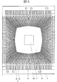
図1は本発明の一実施例であるQFP型半導体装置に用いられるリードフレームを示す平面図であり、図2は図1に示すリードフレームの縦断面図である。リードフレーム1は、例えばFe‐Ni系合金からなり、中央の半導体チップ(破線にて示す)搭載領域2の全周囲にわたって複数のリード3のインナーリード4の先端が配置されている。また、前記リードフレーム1は、Cu系合金でもよい。
FIG. 1 is a plan view showing a lead frame used in a QFP semiconductor device according to an embodiment of the present invention, and FIG. 2 is a longitudinal sectional view of the lead frame shown in FIG. The
各リード3は、ダムバー6により、或はリードフレームの枠体となるタイバー19により一体となっており、各リード3のダムバー6内側部分及び外側部分が夫々インナーリード4及びアウターリード5となる。
Each
このようなリードパターンは、周知のエッチング技術、あるいはプレス技術などによって形成され、通常のQFP型半導体装置では、リード3は数十本から数百本が配置され、本実施例では104本のリード3が配置されている。各リード3のインナーリード4の先端は、支持体の全面に形成された絶縁性の接着剤7によって支持体8の表面に固定されている。
Such a lead pattern is formed by a well-known etching technique or pressing technique. In a normal QFP type semiconductor device, several tens to several hundred
本発明に係るリードフレーム1では、インナーリード4に固定された支持体8の半導体チップ搭載領域2に半導体チップを固定する。このため、半導体チップを搭載するタブ(ダイパッド)を支持するタブ吊りリードは設けられておらず、タブ吊りリードの設けられていた領域をインナーリード4の配置に利用している。
In the
このために、従来タブ吊りリードの設けられていたコーナー部にもインナーリード4が配置されており、該部を含む全周囲にて、各インナーリード先端の間隔であるリードピッチについては、最大のリードピッチが最小のリードピッチの2倍未満となっており、各インナーリード4間には他のリードを配置する余地はなくなっている。つまり、隣接するインナーリードの先端における許容すべき最大のリード間隔(L)と、リードフレームの加工精度、或は設計値により予め決定される最小のインナーリード間隔(W1)及び最小のインナーリード幅(W2)の関係が次の(式1)を満たすように、本形態のリードフレームは作成されている。 For this reason, the inner leads 4 are also arranged at the corners where the tab suspension leads are conventionally provided, and the lead pitch, which is the interval between the tips of the inner leads, is the maximum around the entire circumference including the portions. The lead pitch is less than twice the minimum lead pitch, and there is no room for another lead between the inner leads 4. That is, the maximum allowable lead interval (L) at the tip of the adjacent inner lead, the minimum inner lead interval (W1) and the minimum inner lead width determined in advance by the processing accuracy of the lead frame or the design value The lead frame of this embodiment is created so that the relationship of (W2) satisfies the following (Formula 1).
[数1]
(L)<2×(W1)+(W2)……(式1)
そこで本実施例では、前記インナーリード4を、このタブ吊りリードの設けられていた位置を含めた前記半導体チップ搭載領域の全周囲にわたって等間隔に配置することによって、同一のリードピッチであっても、インナーリード4の先端をより半導体チップ搭載領域2に接近させることが可能となる。このため、半導体チップの搭載後にワイヤボンディングを行う際に、ワイヤ長さを短縮することが可能となり、樹脂封止時のワイヤ流れを低減しワイヤ間のショートが低減する。
[Equation 1]
(L) <2 × (W1) + (W2) (Formula 1)
Therefore, in this embodiment, the inner leads 4 are arranged at equal intervals over the entire circumference of the semiconductor chip mounting area including the position where the tab suspension leads are provided, so that the same lead pitch can be obtained. The tip of the
ここで、支持体8には、熱伝導性の良好な材料例えばCu系材料、Al系材料等を用いることによって、半導体装置の放熱性を向上させることができる。
Here, the heat radiation of the semiconductor device can be improved by using a material having good thermal conductivity, such as a Cu-based material or an Al-based material, for the
また、複数のリード3のインナーリード4を支持体8に固定することにより、各リード3の機械的強度が改善されるので、インナーリード4のリードピッチを小さくしても、外部からの力によるインナーリード4の変形が生じにくくなる。このため、ボンディングワイヤ間のショートを防止することが可能となる。
Further, by fixing the inner leads 4 of the plurality of
なお、従来のヒートスプレッダを用いた技術でもタブレスとしたものはあったが、従来はヒートスプレッダが放熱の問題としてのみ捉えられていた。本発明によれば、これを積極的にリードピッチの問題解決に利用し、ボンディングの安定性を向上させるものである。 Although some conventional techniques using a heat spreader are tabless, the heat spreader has been regarded only as a problem of heat dissipation. According to the present invention, this is actively used for solving the problem of the lead pitch, and the stability of bonding is improved.
次に、図1に示すリードフレーム及びそれを用いた半導体装置の製造方法について図2、図3及び図4を用いて説明する。 Next, a method for manufacturing the lead frame shown in FIG. 1 and a semiconductor device using the lead frame will be described with reference to FIGS.
先ず、図3中(a)に示すように、予め支持体8のインナーリード4と接着される面の全面に接着剤7を塗布形成する。接着剤としては、例えばエポキシ樹脂、フェノール樹脂等の熱硬化性樹脂、或はポリエチレン、塩化ビニール樹脂等の熱可塑性樹脂等が用いられる。支持体8は、金属の薄板を打ち抜き等によって加工したものであるが、接着剤7の塗布はこの加工前でも加工後であってもよい。
First, as shown in FIG. 3A, the adhesive 7 is applied and formed in advance on the entire surface of the
全面に接着剤7を塗布することで、接着剤塗布時のマスキング等を不要にし、支持体8を有するリードフレームの製造コストを低減できる。
By applying the adhesive 7 to the entire surface, masking or the like at the time of applying the adhesive becomes unnecessary, and the manufacturing cost of the lead frame having the
次に、図3中(b)に示すように、パターニングされたリードフレーム1の各インナーリード4を、接着剤7によって支持体8に接着する。この状態が図2となる。本形態の場合は、300℃程度の熱処理によって、接着剤7をキュアし接着した。
Next, as shown in FIG. 3B, the inner leads 4 of the
次に、図3中(c)に示すように、半導体チップ10をAgペースト12によって支持体8の半導体チップ搭載領域2に接着する。従来は、インナーリード4に接着剤7を塗布し支持体8に接着する方法が採られていたが、この方法では接着剤の塗布時にインナーリードを変形させてしまうために不良品となる等の問題があったが、本発明では予め支持体8に塗布した接着剤7によって、インナーリード4の接着を行なうことにより、前述した問題を解決することが可能となる。
Next, as shown in FIG. 3C, the
この後、図4に示すように、半導体チップ10のパッド電極11とインナーリード4とがAu等のボンディングワイヤ13によって接続するが、このワイヤボンディングの際に、本実施例では、インナーリード4が支持体8に固定されているので、この支持体8の裏面を真空吸引することによって、インナーリード4を固定してワイヤボンディングを行うことができるので、従来のリードフレームのごとくインナーリードを押圧固定するウインドクランパを用いる必要がない。
Thereafter, as shown in FIG. 4, the
ワイヤボンディング終了後に、半導体チップ10、支持体8、ボンディングワイヤ13及びインナーリード4が例えばエポキシ樹脂からなる封止体14によって封止され、前述したダムバー6及びタイバー19が切断されて各リード3は電気的に分離される。この後、封止体14から延在するアウターリード5は、一例として図4ではガルウイング状に成形されて半導体装置9が完成する。
After the wire bonding is completed, the
次に、本発明の他の実施例である半導体装置を図5及び図6を用いて説明する。図5は半導体チップ10のパッド電極11の配置を説明する平面図であり、図6は半導体チップ10のコーナー部分のボンディング状態を説明する部分拡大平面図である。
Next, a semiconductor device according to another embodiment of the present invention will be described with reference to FIGS. FIG. 5 is a plan view for explaining the arrangement of the
本実施例の半導体装置では、インナーリード4に固定された支持体8の半導体チップ搭載領域に半導体チップ10を固定する。このため、半導体チップ10を搭載するタブ(ダイパッド)を支持するタブ吊りリードは設けられておらず、タブ吊りリードの設けられていた領域をインナーリード4の配置に利用している。
In the semiconductor device of this embodiment, the
このために、従来タブ吊りリードの設けられていたコーナー部にもインナーリード4が配置されており、該部を含む全周囲にて各インナーリード先端の間隔であるリードピッチについては、全周囲にわたって略等間隔に配置されており、同一のリードピッチであっても、インナーリード4の先端をより半導体チップ10に接近させることが可能となる。なお、各インナーリード4の先端のリードピッチPは、180μm〜220μm程度に設定される。
For this reason, the inner leads 4 are also arranged at the corners where the tab suspension leads are conventionally provided, and the lead pitch, which is the distance between the tips of the inner leads around the entire periphery including the portions, is extended over the entire periphery. The tips of the inner leads 4 can be brought closer to the
半導体チップ10の外部端子となるパッド電極11は、半導体チップ10の周縁部に複数設けられているが、本実施例では、半導体チップのコーナーに近づくにつれてパッドピッチを広く設けてある。
A plurality of
図6に示す例では、半導体チップ10のパッド電極11の内周縁部中央よりのパッドピッチをP1とした場合に、以降のパッドピッチをコーナーに近づくにつれて、P2=1.1P1,P3=1.2P1,P4=1.3P1と0.1P1ずつ広くする構成となっている。なお、高集積度の半導体装置に用いられる半導体チップ10では、パッド電極11のピッチは80μm〜100μm程度に設定される。
In the example shown in FIG. 6, when the pad pitch from the center of the inner peripheral edge of the
パッド電極11とインナーリード4の先端とは、ワイヤ13によって接続するボンディングが行なわれているが、パッド電極11はコーナーに近づくにつれて、パッドピッチが広く配置されているので、コーナー部分のワイヤ13がワイヤ流れなどによって変形した場合でも隣接するワイヤ13と接触しショートするのを防止することができる。なお、ボンディングワイヤ13としては、直径が25μm〜35μm程度のAu細線等が用いられている。
The
また、半導体チップ10は、ワイヤ13の取り回し等の点から、周縁部外端のパッド電極11と半導体チップ10のコーナーを挟んで隣接する他の周縁部外端のパッド電極11とのパッドピッチP5は、他のパッドピッチより広くなっており、この部分ではリードピッチP6よりも広くなっている。
Further, the
また、ワイヤボンディングの際に、本実施例では、インナーリード4が支持体8に固定されているので、この支持体8の裏面を真空吸引することによって、インナーリード4を固定してワイヤボンディングを行うことができるので、従来のリードフレームのごとくインナーリードを押圧固定するウインドクランパを用いる必要がない。
Further, in this embodiment, since the
ワイヤボンディング終了後に、半導体チップ10、支持体8、ボンディングワイヤ13及びインナーリード4が例えばエポキシ樹脂からなる封止体14によって封止され、ダムバー6及び前記タイバー19が切断されて各リード3は電気的に分離され、封止体14から延在するアウターリード5は、一例として図4ではガルウイング状に成形されて半導体装置9が完成する。
After the wire bonding is completed, the
このような本実施例の半導体装置では、ワイヤ流れによる不良品の発生を従来に比較して略半分に低減することができる。 In such a semiconductor device of this embodiment, the generation of defective products due to the wire flow can be reduced to about half compared to the conventional case.
なお、前記パッドピッチの拡げ方としては、前述した周縁部中央から一律に拡げる方法の他に、コーナー部を部分的に拡げる方法等によっても本発明は実施が可能である。 In addition, as the method of expanding the pad pitch, the present invention can be implemented not only by the above-described method of uniformly expanding from the center of the peripheral portion but also by a method of partially expanding the corner portion.
次に、本発明の他の実施例である半導体装置を図7及び図16を用いて説明する。 Next, a semiconductor device according to another embodiment of the present invention will be described with reference to FIGS.
図7は本発明の他の実施例であるQFP型半導体装置に用いられるリードフレームを部分的に示す平面図であり、図16は半導体装置を部分的に示す平面図である。 FIG. 7 is a plan view partially showing a lead frame used in a QFP type semiconductor device according to another embodiment of the present invention, and FIG. 16 is a plan view partially showing the semiconductor device.
リードフレーム1は、例えばFe‐Ni系合金又は、Cu系合金からなり、中央の半導体チップ(破線にて示す)搭載領域2の全周囲にわたって複数のリード3のインナーリード4の先端が配置されている。
The
各リード3のインナーリード4及び半導体チップ10は、絶縁性の接着剤によって支持体8の表面に固定されている。接着剤としては、例えばエポキシ樹脂、フェノール樹脂等の熱硬化性樹脂、或はポリエチレン、塩化ビニール樹脂等の熱可塑性樹脂等が用いられる。
The
本実施例の半導体装置では、インナーリード4に固定された支持体8の半導体チップ搭載領域に半導体チップ10を固定する。このため、半導体チップ10を搭載するタブ(ダイパッド)を支持するタブ吊りリードは設けられておらず、タブ吊りリードの設けられていた領域をインナーリード4の配置に利用することができる。
In the semiconductor device of this embodiment, the
そこで本実施例では、インナーリード4の先端を、半導体チップ搭載領域2の全周囲に配置し、半導体チップ搭載領域2のコーナー部に対応するインナーリード4先端のリードピッチを他のインナーリード4先端のリードピッチよりも広くすることが可能となる。このため、半導体チップの搭載後にワイヤボンディングを行う際に、ワイヤ13相互の間隔が広くなり、ワイヤ13間のショートが低減する。
Therefore, in this embodiment, the tips of the inner leads 4 are arranged around the entire periphery of the semiconductor
ここで、支持体8には、熱伝導性の良好な材料例えばCu系材料、Al系材料等を用いることによって、半導体装置の放熱性を向上させることができる。
Here, the heat radiation of the semiconductor device can be improved by using a material having good thermal conductivity, such as a Cu-based material or an Al-based material, for the
また、複数のリード3のインナーリード4を支持体8に固定することにより、各リード3の機械的強度が改善されるので、インナーリード4のリードピッチを小さくしても、外部からの力による変形が生じにくくなる。このため、ボンディングワイヤ13間のショートを防止することが可能となる。
Further, by fixing the inner leads 4 of the plurality of
また、パッド電極11は、半導体チップ10の周縁部に複数設けられているが、本実施例では、半導体チップのコーナーに近づくにつれてパッドピッチを広く設けてある。なお、高集積度の半導体装置に用いられる半導体チップ10では、パッド電極11のピッチは80μm〜100μm程度に設定される。
Further, a plurality of
パッド電極11とインナーリード4の先端とは、ワイヤ13によって接続するボンディングが行なわれているが、パッド電極11はコーナーに近づくにつれて、パッドピッチが広く配置されているので、コーナー部分のワイヤ13がワイヤ流れなどによって変形した場合でも隣接するワイヤ13と接触しショートするのを防止することができる。なお、ボンディングワイヤ13としては、直径が25μm〜35μm程度のAu細線等が用いられている。
The
また、半導体チップ10は、ある程度の汎用性をもたせるために、周縁部外端のパッド電極11と隣接する他の周縁部外端のパッド電極11とのパッドピッチは、他のパッドピッチより広くなっており、リードピッチよりも広くなることもある。このような場合に前記外端のパッド電極11をよりコーナーに近付けてパッドピッチの拡大を図ることも可能である。
In addition, in order to provide the
また、ワイヤボンディングの際に、本実施例では、インナーリード4が支持体8に固定されているので、この支持体8の裏面を真空吸引することによって、インナーリード4を固定してワイヤボンディングを行うことができるので、従来のリードフレームのごとくインナーリードを押圧固定するウインドクランパを用いる必要がない。
Further, in this embodiment, since the
ワイヤボンディング終了後に、半導体チップ10、支持体8、ボンディングワイヤ13及びインナーリード4が例えばエポキシ樹脂からなる封止体14によって封止され、ダムバー6及び前記タイバー19が切断されて各リード3は電気的に分離され、封止体14から延在するアウターリード5は成形されて半導体装置9が完成する。
After the wire bonding is completed, the
このような本実施例の半導体装置では、ワイヤ流れによる不良品の発生を従来に比較して略半分に低減することができる。 In such a semiconductor device of this embodiment, the generation of defective products due to the wire flow can be reduced to about half compared to the conventional case.
なお、前記パッドピッチの拡げ方としては、前述した周縁部中央から一律に拡げる方法の他に、コーナー部を部分的に拡げる方法等によっても本発明は実施が可能である。 In addition, as the method of expanding the pad pitch, the present invention can be implemented not only by the above-described method of uniformly expanding from the center of the peripheral portion but also by a method of partially expanding the corner portion.
次に、本発明の他の実施例であるリードフレームを図17を用いて説明する。図17はリードフレームを説明する部分拡大平面図である。 Next, a lead frame according to another embodiment of the present invention will be described with reference to FIG. FIG. 17 is a partially enlarged plan view for explaining the lead frame.
本実施例のリードフレーム1では、インナーリード4に固定された支持体8の半導体チップ搭載領域2に半導体チップ(破線にて示す)を固定する。このため、半導体チップ10を搭載するタブ(ダイパッド)を支持するタブ吊りリードは設けられておらず、タブ吊りリードの設けられていた領域をインナーリード4の配置に利用している。
In the
このようなインナーリード4の配置を行なった場合には、コーナー部におけるアウターリード5の配置については、アウターリード5の保護或は樹脂注入流路の確保等のために、封止体14のコーナーから若干離してアウターリード5が配置されることとなる。このため、封止体14のコーナー部ではインナーリード4が配置されない空間が生じてしまうことがある。
When such an
このような空間が生じた場合には、樹脂注入時にこの部分にて注入された樹脂の流れに乱れが生じるためにボイドが発生し樹脂注入不良の原因となることがある。 When such a space is generated, the flow of the resin injected at this portion is disturbed at the time of resin injection, so that voids may be generated and cause resin injection failure.
このような問題を解決するために本実施例では、従来タブ吊りリードの設けられていたコーナー部に、リードフレーム切除後は封止体外に導出しないダミーのインナーリードであるダミーリード20を設ける。ダミーリード20は、他のインナーリード4よりも幅広で先端がインナーリード4の先端よりも外方に設けられており、インナーリード4の先端は、半導体チップ搭載領域2の全周囲にわたって配置されている。
In order to solve such a problem, in this embodiment, dummy leads 20 that are dummy inner leads that are not led out of the sealing body after the lead frame is cut off are provided at the corners where the tab-suspended leads are conventionally provided. The
本実施例ではこのダミーリード20によって樹脂の流れに乱れが生じるのを防止する。従って、このような本実施例の半導体装置では、ボイドによる樹脂注入不良品の発生を低減することができる。
In this embodiment, the
また、支持板8の四隅を幅広のダミーリード20で固定することによって、支持板8をより強固に支持することが可能となる。
Further, the
更に、リードフレームの状態で工程間を搬送するリードフレーム搬送では、リードフレーム切断前のこのダミーリード20の封止体導出部を保持することによって搬送を行なうことが可能であり、アウターリード5を保持して搬送することにより生じるアウターリード5の変形を防止することができる。
Furthermore, in the lead frame transport that transports between processes in the state of the lead frame, it is possible to transport the
次に、本発明の他の実施例である半導体装置を図18及び図19を用いて説明する。図18は本発明者が本発明に至る段階で検討した半導体装置を説明する部分拡大平面図であり、図19は本実施例の半導体装置を説明する部分拡大平面図である。 Next, a semiconductor device according to another embodiment of the present invention will be described with reference to FIGS. FIG. 18 is a partially enlarged plan view for explaining the semiconductor device studied by the present inventors at the stage of reaching the present invention, and FIG. 19 is a partially enlarged plan view for explaining the semiconductor device of this embodiment.
図18に示す半導体装置では、インナーリードと半導体チップのパッド電極との接続は、インナーリードと、このインナーリードに対向する半導体チップの辺に設けられたパッド電極とが接続されている。 In the semiconductor device shown in FIG. 18, the inner lead is connected to the pad electrode of the semiconductor chip by connecting the inner lead and the pad electrode provided on the side of the semiconductor chip facing the inner lead.
しかしながら、同一の半導体チップを異種の封止体に封止する必要がある場合等に、前記半導体チップのコーナー部に対応するインナーリード先端が、このインナーリードと対向する半導体チップの辺とコーナーを挟んで隣接する他の辺に設けられた半導体チップのパッド電極と接続されるクロスボンディングが要求されることがある。 However, when it is necessary to seal the same semiconductor chip in a different type of sealing body, the tip of the inner lead corresponding to the corner portion of the semiconductor chip has the side and corner of the semiconductor chip facing the inner lead. In some cases, cross bonding is required to be connected to pad electrodes of semiconductor chips provided on other sides adjacent to each other.
このような場合に、図18に示す如く半導体チップ10をタブ21に固定し、このタブ21をタブ吊りリード22によって支持する従来の半導体装置では、ボンディングワイヤ13がタブ吊りリード22上を横切ることとなる。このため、ボンディングワイヤ13とタブ吊りリード22との接触による不良の発生を防止するために、このようなボンディングには種々の制限が設けられており、ボンディングが困難であった。
In such a case, in the conventional semiconductor device in which the
本実施例の半導体装置では、インナーリード4に固定された支持体8に半導体チップ10を固定する。このため、半導体チップ10を搭載するタブ21(ダイパッド)及びこのタブを支持するタブ吊りリード22は設けられておらず、タブ吊りリード22の設けられていた領域をインナーリード4の配置に利用している。
In the semiconductor device of the present embodiment, the
このようなインナーリード4の配置を行なうことによって、前述したクロスボンディングを行なっても、ボンディングワイヤ13とタブ吊りリード22との接触による不良の発生がなくなり、製品の信頼性が向上することとなる。
By arranging the inner leads 4 in this way, even if the above-described cross bonding is performed, the occurrence of defects due to the contact between the
また、前記クロスボンディングを容易に行なうことが可能となり、ボンディングの自由度が向上することとなる。 Further, the cross bonding can be easily performed, and the degree of freedom of bonding is improved.
図8は本発明の他の実施例であるリードフレームを示す断面図であり、図9はこのリードフレームを用いて製造した半導体装置を示す縦断面図である。 FIG. 8 is a sectional view showing a lead frame according to another embodiment of the present invention, and FIG. 9 is a longitudinal sectional view showing a semiconductor device manufactured using the lead frame.
本実施例によるリードフレーム1は、既述した実施例によるリードフレームの構成に加えて、支持体8の半導体チップ搭載領域2とインナーリード4先端との間に、ワイヤ支持部15を設けたことを特徴としている。
In the
このワイヤ支持部15は、支持体8の搭載領域2の周囲に配置され、半導体装置を組み立てるとき、半導体チップのパッド電極と各リードとの間にボンディングされるワイヤのループを一定の高さに支持することができる。ワイヤ支持部15は、例えばポリイミド樹脂、エポキシ樹脂などの絶縁材料を接着剤等によって支持体8に固定する、或は、支持体8を部分的に加工して、少なくともワイヤが接する部分を絶縁処理することによって形成する。
The
このような、実施例によるリードフレーム1によれば、ボンディングワイヤを支持するワイヤ支持部15を有しているので、ワイヤのループ高さを一定に確保することができるため、ワイヤ相互のショートを低減することができるという効果が得られる。
According to such a
図10は本発明の他の実施例であるリードフレームを示す断面図であり、図11はこのリードフレームを用いて製造した半導体装置を示す縦断面図である。 FIG. 10 is a sectional view showing a lead frame according to another embodiment of the present invention, and FIG. 11 is a longitudinal sectional view showing a semiconductor device manufactured using the lead frame.
本実施例によるリードフレーム1は、既述した実施例によるリードフレームの構成に加えて、支持体8の半導体チップ搭載領域2とインナーリード4先端との間に、支持体8を保持する治具16に設けたワイヤ支持部15を突出させるスリット17を設けたことを特徴としている。
The
リードフレーム1を治具16保持した際に、治具16に設けられたワイヤ支持部15が、このスリット17から突出することとなる。ワイヤ支持部15は、ワイヤボンディング終了後にスリット17から退避することとなるので、絶縁性の有無を問われない。
When the
本実施例では、治具16に設けたワイヤ支持部15をリードフレーム1のスリット17に挿入することにより、ボンディングが安定するという効果が得られる。
In the present embodiment, by inserting the
図12は本発明の他の実施例であるリードフレームを示す断面図であり、図13はこのリードフレームを用いて製造した半導体装置を示す縦断面図である。 FIG. 12 is a cross-sectional view showing a lead frame according to another embodiment of the present invention, and FIG. 13 is a vertical cross-sectional view showing a semiconductor device manufactured using this lead frame.
本実施例によるリードフレーム1は、既述した実施例によるリードフレームの構成に加えて、支持体8の半導体チップ搭載領域2が、搭載する半導体チップ10のパッド電極11とインナーリード4表面とが略同じ高さとなるべくオフセットされていることを特徴としている。このようなオフセット形状は、周知のプレス技術などを利用することにより容易に加工することができる。
In the
このような加工を行なうことによって、インナーリード4表面の高さ位置H1と搭載される半導体チップ10の表面の高さ位置H2とを略等しくすることにより、半導体チップ10のパッド電極11と各インナーリード4とのワイヤボンディングの際に、ボンディングされるワイヤ13のループの安定性を高めることができる。ワイヤ13のループの安定性を高めることによって、ループ形状が一定となるので樹脂モールド時におけるワイヤ流れを減少することが可能となる。
By performing such processing, the height position H1 of the surface of the
図14は本発明の他の実施例であるリードフレームに用いられる支持体8を示す平面図であり、図15はこの支持体8に半導体チップ10を搭載した状態を示す平面図である。
FIG. 14 is a plan view showing a
本実施例によるリードフレーム1は、既述した実施例によるリードフレーム1の構成に加えて、支持体8の表面に、搭載される半導体チップ10の各種寸法に対応した複数のマーカ18を設けたことを特徴としている。このようなマーカ18は、印刷、プレスなどの技術によって、容易に設けることができる。
The
このように、搭載される半導体チップのサイズに対応したマーカ18を設けることにより、半導体チップを搭載する際に、半導体チップを搭載する正確な位置の確認が容易になるので、半導体チップのチップボンディング作業の効率が向上する。
Thus, by providing the
更に、半導体チップの位置決め精度が向上するので、ワイヤの長さを一定に保つことが可能となり、ボンディングワイヤのループを安定に保つことができる。ワイヤのループの安定性を高めることによって、ループ形状が一定となるので樹脂モールド時におけるワイヤ流れを減少することが可能となる。 Furthermore, since the positioning accuracy of the semiconductor chip is improved, the wire length can be kept constant, and the bonding wire loop can be kept stable. By increasing the stability of the wire loop, the loop shape becomes constant, so that the wire flow during resin molding can be reduced.
以上、本発明者によってなされた発明を、前記実施例に基づき具体的に説明したが、本発明は、前記実施例に限定されるものではなく、その要旨を逸脱しない範囲において種々変更可能であることは勿論である。 As mentioned above, the invention made by the present inventor has been specifically described based on the above embodiments. However, the present invention is not limited to the above embodiments, and various modifications can be made without departing from the scope of the invention. Of course.
例えば、前記実施例では各リードが固定される支持体として方形状のものを例示したが、支持体として円形状のものを用いることも可能である。このような円形状の支持体を用いた場合には、樹脂モールド時に樹脂の流れがスムーズになるので、ボイドの発生を減少できるという効果が得られる。 For example, in the above embodiment, a rectangular support is illustrated as the support to which each lead is fixed, but a circular support may be used as the support. When such a circular support is used, the flow of the resin becomes smooth during resin molding, so that the effect of reducing the generation of voids can be obtained.
また、前記実施例で用いた支持体にアースボンドを目的としたボンディングエリアを設けることによって、アースボンド対応可能なリードフレームとして更に広い用途への適用が可能となる。 In addition, by providing a bonding area for the purpose of ground bonding on the support used in the above-described embodiments, it is possible to apply to a wider range of uses as a lead frame that can handle ground bonding.
さらに、支持体に対して搭載する半導体チップは1個に限定されず、複数個の半導体チップを搭載することも可能であり、これによりマルチチップの半導体装置に本発明を適用することも可能である。 Further, the number of semiconductor chips to be mounted on the support is not limited to one, and a plurality of semiconductor chips can be mounted, whereby the present invention can be applied to a multi-chip semiconductor device. is there.
以上の説明では、主として本発明者によってなされた発明をその背景となった利用分野である半導体装置に適用した場合について説明したが、それに限定されるものではなく、本発明は、リードフレームを用いて電子部品を実装するものには広く適用が可能である。 In the above description, the case where the invention made mainly by the present inventor is applied to the semiconductor device which is the field of use behind it has been described. However, the present invention is not limited to this, and the present invention uses a lead frame. Therefore, it can be widely applied to those mounting electronic parts.
1…リードフレーム、2…半導体チップ搭載領域、3…リード、4…インナーリード、5…アウターリード、6…ダムバー、7…接着剤、8…支持体、9…半導体装置、10…半導体チップ、11…パッド電極、12…接着剤、13…ボンディングワイヤ、14…封止体、15…ワイヤ支持部、16…治具、17…スリット、18…マーカ、19…タイバー、20…ダミーリード、21…タブ、22…タブ吊りリード、P1,P2,P3,P4,P5…パッド電極のピッチ、P6…コーナー部のリードピッチ、H1…支持体の表面の高さ位置、H2…支持体の中央位置(半導体チップの搭載位置)の高さ位置。
DESCRIPTION OF
Claims (2)
前記支持体の一表面に搭載され、集積回路と主要表面上に形成された複数のパッド電極とを有し、前記主要表面が四辺形となり、前記パッド電極が前記四辺形の4つの辺に沿って配設されてなる半導体チップと、
前記4つの辺に沿って前記半導体チップを取り囲むように前記支持体の前記一表面上に絶縁接着剤層によって固定されるインナーリード及びこのインナーリードに連続するアウターリードとからなる複数のリードと、
前記パッド電極と前記インナーリードの先端を電気的に接続する複数のボンディングワイヤと、
前記半導体チップ、前記インナーリード、前記複数のボンディングワイヤ及び前記支持体を封止する四辺形からなる封止体とを有し、
前記アウターリードは前記半導体チップの前記4つの辺と向かい合う前記封止体の4つの辺から外方向に突出する半導体装置であって、
前記封止体の4つの各コーナーにおいて、前記封止体の隣接する2つの辺からそれぞれ突出している隣接する2つのリードのインナーリード先端の最大ピッチが、前記半導体チップを取り囲む前記インナーリードのそれぞれの先端ピッチに関して最小ピッチの2倍未満であり、隣接するボンディングパッド間のピッチが前記4つの辺によって定まるコーナに向かうに従って増大し、
前記封止体の4つの各コーナーに前記支持体に接続されるダミーリードが設けられていることを特徴とする半導体装置。 A support;
The integrated circuit and a plurality of pad electrodes formed on the main surface are mounted on one surface of the support, the main surface is a quadrilateral, and the pad electrode is along the four sides of the quadrilateral. A semiconductor chip arranged with
A plurality of leads comprising an inner lead fixed by an insulating adhesive layer on the one surface of the support so as to surround the semiconductor chip along the four sides, and an outer lead continuous with the inner lead;
A plurality of bonding wires that electrically connect the pad electrode and the tip of the inner lead;
The semiconductor chip, the inner lead, the plurality of bonding wires and a sealing body made of a quadrangle that seals the support,
The outer lead is a semiconductor device protruding outward from four sides of the sealing body facing the four sides of the semiconductor chip,
At each of the four corners of the sealing body, the maximum pitch of the inner lead tips of the two adjacent leads protruding from the two adjacent sides of the sealing body is such that each of the inner leads surrounding the semiconductor chip. Less than twice the minimum pitch, and the pitch between adjacent bonding pads increases toward the corner defined by the four sides,
A semiconductor device, wherein dummy leads connected to the support are provided at each of the four corners of the sealing body.
前記支持体の一表面に搭載され、集積回路と主要表面上に形成された複数のパッド電極とを有し、前記主要表面が四辺形となり、前記パッド電極が前記四辺形の4つの辺に沿って配設されてなる半導体チップと、
前記4つの辺に沿って前記半導体チップを取り囲むように前記支持体の前記一表面上に絶縁接着剤層によって固定されるインナーリード及びこのインナーリードに連続するアウターリードとからなる複数のリードと、
前記パッド電極と前記インナーリードの先端を電気的に接続する複数のボンディングワイヤと、
前記半導体チップ、前記インナーリード、前記複数のボンディングワイヤ及び前記支持体を封止する四辺形からなる封止体とを有し、
前記アウターリードは前記半導体チップの前記4つの辺と向かい合う前記封止体の4つの辺から外方向に突出する半導体装置であって、
前記封止体の4つの各コーナーにおいて、前記封止体の隣接する2つの辺からそれぞれ突出している隣接する2つのリード先端の最大ピッチが、前記半導体チップを取り囲む前記インナーリードのそれぞれの先端ピッチに関して最小ピッチの2倍未満であり、
前記封止体の4つの各コーナーに前記支持体に接続されるダミーリードが設けられていることを特徴とする半導体装置。 A support;
The integrated circuit and a plurality of pad electrodes formed on the main surface are mounted on one surface of the support, the main surface is a quadrilateral, and the pad electrode is along the four sides of the quadrilateral. A semiconductor chip arranged with
A plurality of leads comprising an inner lead fixed by an insulating adhesive layer on the one surface of the support so as to surround the semiconductor chip along the four sides, and an outer lead continuous with the inner lead;
A plurality of bonding wires that electrically connect the pad electrode and the tip of the inner lead;
The semiconductor chip, the inner lead, the plurality of bonding wires and a sealing body made of a quadrangle that seals the support,
The outer lead is a semiconductor device protruding outward from four sides of the sealing body facing the four sides of the semiconductor chip,
At each of the four corners of the sealing body, the maximum pitch of the two adjacent lead tips protruding from the two adjacent sides of the sealing body is the tip pitch of each of the inner leads surrounding the semiconductor chip. Less than twice the minimum pitch,
A semiconductor device, wherein dummy leads connected to the support are provided at each of the four corners of the sealing body.
Priority Applications (1)
| Application Number | Priority Date | Filing Date | Title |
|---|---|---|---|
| JP2004012736A JP4015118B2 (en) | 1996-03-18 | 2004-01-21 | Semiconductor device |
Applications Claiming Priority (2)
| Application Number | Priority Date | Filing Date | Title |
|---|---|---|---|
| JP6042196 | 1996-03-18 | ||
| JP2004012736A JP4015118B2 (en) | 1996-03-18 | 2004-01-21 | Semiconductor device |
Related Parent Applications (1)
| Application Number | Title | Priority Date | Filing Date |
|---|---|---|---|
| JP9008964A Division JPH09312375A (en) | 1996-03-18 | 1997-01-21 | Lead frame, semiconductor device and manufacture thereof |
Publications (3)
| Publication Number | Publication Date |
|---|---|
| JP2004158875A JP2004158875A (en) | 2004-06-03 |
| JP2004158875A5 JP2004158875A5 (en) | 2005-09-15 |
| JP4015118B2 true JP4015118B2 (en) | 2007-11-28 |
Family
ID=32827161
Family Applications (1)
| Application Number | Title | Priority Date | Filing Date |
|---|---|---|---|
| JP2004012736A Expired - Fee Related JP4015118B2 (en) | 1996-03-18 | 2004-01-21 | Semiconductor device |
Country Status (1)
| Country | Link |
|---|---|
| JP (1) | JP4015118B2 (en) |
Families Citing this family (1)
| Publication number | Priority date | Publication date | Assignee | Title |
|---|---|---|---|---|
| JP6100648B2 (en) | 2013-08-28 | 2017-03-22 | ルネサスエレクトロニクス株式会社 | Semiconductor device and manufacturing method of semiconductor device |
-
2004
- 2004-01-21 JP JP2004012736A patent/JP4015118B2/en not_active Expired - Fee Related
Also Published As
| Publication number | Publication date |
|---|---|
| JP2004158875A (en) | 2004-06-03 |
Similar Documents
| Publication | Publication Date | Title |
|---|---|---|
| US6265762B1 (en) | Lead frame and semiconductor device using the lead frame and method of manufacturing the same | |
| US20190027427A1 (en) | Semiconductor device | |
| US8178955B2 (en) | Semiconductor device | |
| US7339259B2 (en) | Semiconductor device | |
| KR100596100B1 (en) | A method of manufacturing a semiconductor device | |
| JPH0815193B2 (en) | Semiconductor device and lead frame used for the same | |
| JP2000307045A (en) | Lead frame and manufacture of resin sealed semiconductor device using it | |
| JP3072291B1 (en) | Lead frame, resin-encapsulated semiconductor device using the same and method of manufacturing the same | |
| JPS5992556A (en) | Semiconductor device | |
| JP3430976B2 (en) | Lead frame, resin-sealed semiconductor device using the same, and method of manufacturing the same | |
| JPH08139218A (en) | Hybrid integrated circuit device and its manufacture | |
| JPH09307051A (en) | Semiconductor device sealed by resin and method of manufacturing it | |
| JP4015118B2 (en) | Semiconductor device | |
| US6909179B2 (en) | Lead frame and semiconductor device using the lead frame and method of manufacturing the same | |
| JPH04236434A (en) | Semiconductor device and manufacture thereof | |
| JPH10242362A (en) | Lead frame, semiconductor device and manufacture of semiconductor device | |
| JPH11260989A (en) | Resin-sealed semiconductor device and its manufacture | |
| JP3454192B2 (en) | Lead frame, resin-sealed semiconductor device using the same, and method of manufacturing the same | |
| JP2002164496A (en) | Semiconductor device and method for manufacturing the same | |
| JPH05211274A (en) | Lead frame and semiconductor device | |
| JP2002009116A (en) | Semiconductor device and method of manufacturing same | |
| JP2750916B2 (en) | Semiconductor device and manufacturing method thereof | |
| TW201635447A (en) | Quad flat non-leaded package structure and leadframe thereof | |
| JPH08148634A (en) | Lead frame, semiconductor device using it, and manufacture thereof | |
| JP2003007953A (en) | Resin-sealing semiconductor device and manufacturing method therefor |
Legal Events
| Date | Code | Title | Description |
|---|---|---|---|
| A521 | Written amendment |
Free format text: JAPANESE INTERMEDIATE CODE: A523 Effective date: 20050531 |
|
| A131 | Notification of reasons for refusal |
Free format text: JAPANESE INTERMEDIATE CODE: A131 Effective date: 20070213 |
|
| A521 | Written amendment |
Free format text: JAPANESE INTERMEDIATE CODE: A523 Effective date: 20070411 |
|
| TRDD | Decision of grant or rejection written | ||
| A01 | Written decision to grant a patent or to grant a registration (utility model) |
Free format text: JAPANESE INTERMEDIATE CODE: A01 Effective date: 20070911 |
|
| A61 | First payment of annual fees (during grant procedure) |
Free format text: JAPANESE INTERMEDIATE CODE: A61 Effective date: 20070912 |
|
| FPAY | Renewal fee payment (event date is renewal date of database) |
Free format text: PAYMENT UNTIL: 20100921 Year of fee payment: 3 |
|
| R150 | Certificate of patent or registration of utility model |
Free format text: JAPANESE INTERMEDIATE CODE: R150 |
|
| FPAY | Renewal fee payment (event date is renewal date of database) |
Free format text: PAYMENT UNTIL: 20110921 Year of fee payment: 4 |
|
| FPAY | Renewal fee payment (event date is renewal date of database) |
Free format text: PAYMENT UNTIL: 20110921 Year of fee payment: 4 |
|
| S111 | Request for change of ownership or part of ownership |
Free format text: JAPANESE INTERMEDIATE CODE: R313115 |
|
| FPAY | Renewal fee payment (event date is renewal date of database) |
Free format text: PAYMENT UNTIL: 20110921 Year of fee payment: 4 |
|
| R350 | Written notification of registration of transfer |
Free format text: JAPANESE INTERMEDIATE CODE: R350 |
|
| FPAY | Renewal fee payment (event date is renewal date of database) |
Free format text: PAYMENT UNTIL: 20120921 Year of fee payment: 5 |
|
| FPAY | Renewal fee payment (event date is renewal date of database) |
Free format text: PAYMENT UNTIL: 20120921 Year of fee payment: 5 |
|
| FPAY | Renewal fee payment (event date is renewal date of database) |
Free format text: PAYMENT UNTIL: 20130921 Year of fee payment: 6 |
|
| LAPS | Cancellation because of no payment of annual fees |