JP4011345B2 - Multi-axis force sensor chip - Google Patents
Multi-axis force sensor chip Download PDFInfo
- Publication number
- JP4011345B2 JP4011345B2 JP2002005334A JP2002005334A JP4011345B2 JP 4011345 B2 JP4011345 B2 JP 4011345B2 JP 2002005334 A JP2002005334 A JP 2002005334A JP 2002005334 A JP2002005334 A JP 2002005334A JP 4011345 B2 JP4011345 B2 JP 4011345B2
- Authority
- JP
- Japan
- Prior art keywords
- force sensor
- sensor chip
- axis
- semiconductor substrate
- axis force
- Prior art date
- Legal status (The legal status is an assumption and is not a legal conclusion. Google has not performed a legal analysis and makes no representation as to the accuracy of the status listed.)
- Expired - Fee Related
Links
Images


Description
【0001】
【発明の属する技術分野】
本発明は、半導体抵抗素子を用いた力覚センサに係わり、力とモーメントの6成分の検知が可能な、小型・高精度な力覚センサに関する。
【0002】
【従来の技術】
近年、工作機械などで、ロボットやマニピュレータが多用されるようになり、かつ対象物の小型化に対応するため、これらロボット用力覚センサやマンマシンインターフェイスとして用いる、高精度な多軸力センサの必要性が高まっている。
多軸力センサは、外力が印加されることによって弾性変形する起歪体に、機械的変形により電気抵抗が変化する歪み抵抗素子を配置し、これらの抵抗素子の抵抗変化を電気信号として取り出して、この電気信号に基づいて、上記起歪体にかかる、2成分以上(例えば、X軸方向とY軸方向)の力の強さを検出する。
【0003】
しかしながら、上記従来例においては、複数個の歪みゲージ(上記歪み抵抗素子等)を、上記起歪体に対して個々に独立して貼付するため、その取り付けの位置精度により、設計通りの、すなわち、各々の歪みゲージから、歪みの程度に対して想定した電圧レベルの電気信号を得ることが困難である。
このため、上記従来例は、取り付け位置の精度に起因して、検出精度を確保することが難しく、さらに同一特性の多軸力センサを再現性良く生産することが困難である。
【0004】
さらに、上記従来例には、複数の歪みゲージを高い位置精度で貼付する必要があるため、貼付工程に手間がかかり、生産性を向上させることができず、かつ小型化も困難となるという欠点がある。
【0005】
加えて、上記従来例には、繰り返しの衝撃荷重の印加により、あるいは貼付された歪みゲージと起歪体との熱膨張率が大きく異なる場合、温度ストレスにより、経時的に起歪体からの歪みゲージの剥がれが発生して、歪みゲージに対して起歪体の歪みが十分に伝達されずに、歪みゲージから正確な電気信号が出力されなくなり、正確な測定できなくなるという問題がある。
【0006】
上述した従来例の問題を解決する多軸力センサとして、半導体プロセスを利用して、半導体単結晶基板に複数の半導体抵抗素子を作成して、起歪体に対する歪みゲージの貼付の必要性を排除することで、起歪体に半導体抵抗素子を貼付する工程の精度の問題を解決し、小型化を可能にする構成が提案されている(特許第2746298号,特公平7−93445)。
【0007】
【発明が解決しようとする課題】
しかしながら、上述した半導体プロセスを利用した多軸力センサにおいては、各軸方向の力又はモーメントの印加に対して基板全体が等方的に歪む構造であり、かつ各半導体抵抗素子の配置が適切でないため、未知方向から印加される外力を各成分に精度良く分離することが困難である。
すなわち、各成分に対応する抵抗素子から検出される電気信号成分に、他軸の成分が重畳してしまい、力又はモーメントの各成分の測定感度が低下してしまう。
【0008】
一般に、多軸力センサの場合、各成分を求めるために、各成分の力又はモーメントと抵抗変化率との関係を示すマトリクスが必要となる。
6軸力センサの場合を例にとり、さらに詳しく説明する。6軸力センサでは、直行するx軸,y軸及びz軸方向それぞれの力Fx,Fy,Fzと、x軸,y軸及びz軸におけるそれぞれのモーメントMx,My,Mzとを求めることができる。これらを各々力F1,F2,F3,F4,F5,F6とする。
また、6軸力センサに配置された各半導体抵抗素子の抵抗変化率から求めた演算抵抗変化率をS1,S2,S3,S4,S5,S6とする。
【0009】
そして、上記演算抵抗変化率Siと力Fiとの間には(iは1〜6の整数)、行列で表すと、
(Si)=(mij)×(Fi) (jは1〜6の整数)
の関係、すなわち、
S1=m11・F1+m12・F2+m13・F3+m14・F4+m15・F5+m16・F6
S2=m21・F1+m22・F2+m23・F3+m24・F4+m25・F5+m26・F6……
S6=m61・F1+m62・F2+m63・F3+m64・F4+m65・F5+m66・F6
の関係がある。
ここで、(Si),(Fi)はi行の行列であり、(mij)はi行j列の行列である。
【0010】
あらかじめ、単一成分のみの入力に対する上記各演算抵抗変化率を求めることにより、行列(mij)の各行列要素mijを求めることができる。
そして、この行列(mij)の逆行列(m'ij)を求めることにより、
(Fi)=(m'ij)×(Si)
の行列計算、すなわち、
F1=m'11・S1+m'12・S2+m'13・S3+m'14・S4+m'15・S5+m'16・S6
F2=m'21・S1+m'22・S2+m'23・S3+m'24・S4+m'25・S5+m'26・S6
……
F6=m'61・S1+m'62・S2+m'63・S3+m'64・S4+m'65・S5+m'66・S6
の関係として、各半導体抵抗素子の抵抗変化率から得られる演算抵抗変化率に基づき、各軸方向の力及びモーメントを求めることができる。
上記各式においては、行列要素mijの数値が各々大きいものであると、例えば、ノイズの重量で抵抗変化率Siが変動するとF1〜F6の測定値にその影響が現れる。
【0011】
すなわち、外力として単一成分のみの入力があったときにその他の成分の入力が「0」であるにもかかわらず、ノイズ等の外乱により測定結果が「0」にならないという現象が起きる可能性が高くなる。
以下、上述したように、求める成分の力又はモーメントの測定値が他軸の力又はモーメントによって変動することを、他軸干渉が起こると定義する。
理想的には、行列(m'ij)において、対角要素m'11,m'22,m'33,m'44,m'55,m'66以外の非対角要素を「0」とし、この行列(m'ij)を対角行列とし、力又はモーメントの各成分と演算抵抗変化率との関係を、
F1=m'11・S1
F2=m'22・S2
……
F6=m'66・S6
のような関数にできれば、計算も簡易となり、他軸干渉も防止することが可能である。
【0012】
実際には、非対角要素を「0」とできなくとも、対角要素に比較して非対角要素の値を非常に小さくすることにより、他軸干渉の影響を低減できることになる。
しかしながら、従来例のような、基板全体が歪み、かつ半導体抵抗素子の配置の考慮がされていない構造の多軸力センサにおいては、行列(m'ij)の非対角要素を「0」、または対角要素に比較して小さくすることができず、他軸干渉が起こる可能性が高くなると考えられる。
すなわち、上記従来の多軸力センサは、他軸干渉が起こり易いことにより、半導体抵抗素子からの電気信号に、予期しない外乱等によるノイズが重畳することにより、他軸干渉により、測定結果が大きく変動してしまう可能性が大きい。
したがって、上記多軸力センサをロボット等に使用した場合においても、その設置状況によって、他軸干渉により測定値が変動することになり、汎用部品とした場合に、再現性やロバスト性に問題がある。
【0013】
上述した半導体プロセスを用いた多軸力センサの欠点を解決するため、軸毎に歪みの成分を分離する構造が提案されている(特開平11−333765)。
この多軸力センサは、すでに述べたセンサに対して改善されてはいるが、3軸(x軸,y軸,z軸)方向の力の検出を行うための構成であり、6軸力センサとして使用する場合に、各成分の分離機能が不十分であり、他軸干渉の問題を改善している訳ではない。
【0014】
本発明はこのような背景の下になされたもので、その目的は印加される外力の検出において、他軸干渉を抑制し、各軸成分の力又はモーメントを検出できる、ロバスト性及び再現性が向上された6軸力センサを提供する事にある。
【0015】
【課題を解決するための手段】
本発明の多軸力センサ(例えば、一実施形態における6軸力センサ1)は、半導体基板(例えば、一実施形態における半導体基板2)からなる多軸力センサ機能を有するセンサチップであり、該センサチップが、外力が印加される作用部(例えば、一実施形態における作用部4)と、外部構造体に固定される支持部(例えば、一実施形態における支持部3)と、前記作用部と前記支持部とを連結する、各々が剛性の高い領域と剛性の低い領域とからなる平面形状を有する少なくとも4本以上からなる連結部(例えば、T字ビーム形状の一実施形態における5A,5B,5C,5D)とから構成され、前記連結部の表面に形成された歪み検出素子(例えば、一実施形態における抵抗素子Sya1〜Sya3,抵抗素子Syb1〜Syb3,抵抗素子Sxa1〜Sxa3,抵抗素子Sxb1〜Sxb3)が配置され、各々の歪み検出素子が前記支持部の対応する電極に配線されている構成のため、上記剛性の低い領域が上記連結部にかかる余分な歪みを吸収し、半導体基板全体の歪みの発生を抑制する機能が有り、特定の軸成分の力又はモーメントが対応する歪み検出素子に選択的に歪みを発生させるので、各歪み検出素子による測定結果の組み合わせにより、印加される外力を効果的に力、モーメントの6成分に分離できるため、測定結果の他軸干渉を大幅に抑制できる。これにより、本発明の多軸力センサは、作用部に印加される外力の力,モーメントの6成分を各連結部に配置した各歪み検出素子に発生する歪みに基づき、再現性良く測定することが可能となる。本発明の多軸力センサ素子は、前記連結部が前記作用部の周囲に等間隔に各々配置されており、前記剛性の低い領域が前記支持部に少なくとも2箇所で接続される弾性部(例えば、一実施形態における弾性部5Ab,5Bb,5Cb,5Db)であり、前記剛性の高い領域が前記作用部と接続される橋梁部(例えば、一実施形態における橋梁部5Aa,5Ba,5Ca,5Da)である構成のため、弾性部が橋梁部にかかる余分な歪みを吸収し、一方向への力又はモーメントの印加による半導体基板全体の歪みの発生を抑制する機能が有り、特定の方向の力又はモーメントに対応する歪み検出素子に選択的に歪みを発生させるので、他軸干渉を大幅に抑制できる。
【0016】
本発明の多軸力センサ素子は、前記橋梁部の表面において、作用部に外力が印加された場合に、前記作用部または前記連結部の他の領域に比較して、大きな歪みの発生する領域に歪み検出素子を配置することにより、歪み検出素子が所望の成分の力又はモーメントを選択的に検知出来るとともに、外力に対する歪み検出素子の感度(歪み検出素子が半導体抵抗素子である場合は抵抗値の変化量)を大きくすることができ、作用部に印加される外力の力及びモーメントの測定感度を向上させ、測定結果におけるロバスト性及び安定性を得ることが可能となる。
【0017】
本発明の多軸力センサ素子は、前記歪み検出素子が前記作用部と前記橋梁部との接続部近傍の表面に配置されることにより、外力により発生する歪みが最も集中する領域に配置されることととなり、外力に対する歪み検出素子の抵抗値の変化量を大きくすることができ、効果的に作用部に印加される外力の力及びモーメントの測定感度を向上させ、測定結果におけるロバスト性及び安定性を得ることが可能となる。
【0018】
本発明の多軸力センサ素子は、前記歪み検出素子が、前記橋梁部に形成されたくびれ部に配置されることにより、作用部に印加された外力の力またはモーメントの各成分に対応する連結部において、くびれ部に発生する応力が最も大きくなるため、このくびれ部に最も歪みが集中することとなり、外力に対する歪み検出素子の抵抗変化を大きくすることができ、効果的に作用部に印加される外力の力及びモーメントの測定感度を向上させ、測定結果におけるロバスト性及び安定性を得ることが可能となる。
【0019】
本発明の多軸力センサ素子は、前記歪み検出素子が、前記橋梁部毎に、その長軸方向に対して平行に複数配置されていることにより、複数の歪み検出素子から得られる抵抗変化率を組み合わせて電気信号を取り出すことが可能となり、他軸干渉を防止するように、すなわち、特定の方向の力又はモーメント以外に対する抵抗変化率が打ち消し合うように、歪み検出素子を選択し、かつこれらの歪み検出素子の抵抗変化率から、力及びモーメントの6成分を求めるのに適した式を構成することができ、この式に基づいて力及びモーメントと抵抗変化率との関係を示す行列における非対角要素を、「0」または十分に小さくすることが可能である。これにより、本発明の多軸力センサは、他軸干渉を抑制することができ、印加される外力の力及びモーメントの多成分の測定精度を向上させ、力及びモーメントの測定結果におけるロバスト性を向上させることが可能となる。
【0020】
本発明の多軸力センサ素子は、前記連結部及び前記作用部の接続部と、該連結部及び前記支持部の接続部と、前記弾性部及び該橋梁部の接続部とにおける内角部が各々円弧状(例えば、一実施形態における、穴の領域A,B,C,D,K,L,M,Nの内周におけるR加工された内角部)に加工形成されていることにより、各接続部における応力を分散させ、作用部に印加される外力に対して、内角部に対する応力集中を抑制し、構造的な強度を向上させるため、印加される外力の測定範囲を広げることが可能となる。
【0021】
本発明の多軸力センサ素子は、温度補償用の半導体抵抗素子(例えば、一実施形態における抵抗素子13)が支持部に配置され、対応する電極(例えば、一実施形態における電極14)に配線されていることにより、設けられている周囲の温度による抵抗変化を検知することができ、歪み検出素子の温度特性に対応して、抵抗変化の測定結果を補正することで、周囲温度に影響されない力及びモーメントの測定を行うことが可能である。
【0022】
本発明の多軸力センサ素子は、接地電位であるガード配線(例えば、一実施形態におけるGND配線7)が、歪み検出素子の接地電位ではない配線(例えば、一実施形態における信号配線8)を、包囲するように配置されることにより、歪み検出素子からの電流を検出する場合、環境中の高周波ノイズによる外乱を押さえ、かつ前記ガード配線が他の歪み検出素子の配線からのクロストークノイズをシールドするため、歪み検出素子の抵抗変化における電流測定のS/N比を向上させることができ、印加される外力の力及びモーメントの測定精度を向上させ、測定結果におけるロバスト性及び安定性を得ることが可能となる。
【0023】
本発明の多軸力センサ素子は、前記半導体基板にバイアスを印加するバイアス電極(例えば、一実施形態におけるバイアス電極12)が形成されていることにより、この印加されるバイアスにより、前記歪み検出素子を形成する半導体抵抗素子の活性層界面に空乏層が成長し、活性層と半導体基板との間,及び隣接する活性層間の絶縁を行うことができるため、リーク電流が減少し、電流ノイズの影響を低減することができる。さらに、電気的に基板を一定電位に固定することにより、電位のふらつき防止やノイズ耐性を向上させることができ、半導体抵抗素子の抵抗変化量を高い精度で測定することができるので、印加される外力の力及びモーメントの測定精度を向上させ、測定結果におけるロバスト性及び安定性を得ることが可能となる。
【0024】
本発明の多軸力センサ素子は、前記半導体基板において、前記橋梁部の前記歪み検出素子が配置される領域に相対する裏面の領域に、少なくとも1個以上の歪み検出素子(例えば、一実施形態における抵抗素子Sya1u〜Sya3u,Sxa1u〜Sxa3u,抵抗素子Syb1u〜Syb1u,Sxb1u〜Sxb3u)が、前記橋梁部の長軸方向に対して平行に形成され、配線により電極に接続されていることにより、表面及び裏面に形成された各々の歪み検出素子の抵抗変化に基づき、作用部に印加される外力の力及びモーメントを、表面のみに歪み検出素子を設けた場合に比較して、より特定成分毎に分離して高い精度で測定することができ、測定結果におけるロバスト性及び安定性を得ることが可能となる。
【0025】
【発明の実施の形態】
以下、図面を参照して本発明の実施形態について説明する。
<6軸力センサの構造及び機能>
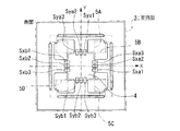
図1は本発明の一実施形態による6軸力センサの構造例を示す上面からみた平面図である。この図において、6軸力センサ1は、半導体基板2上面に形成された活性層(拡散層)よりなるなる抵抗素子(ピエゾ抵抗素子)Sxa1〜Sxa3,Sxb1〜Sxb3,Sya1〜Sya3,Syb1〜Syb3から構成されている(半導体製造技術を用いた1チップ構成)。
半導体基板2は、厚さ方向に貫通した穴の領域A,B,C,D,K,L,M,Nにより、以下に示すセンサ構造を有している。
ここで、穴の領域A,B,C,D,K,L,M,Nの内周における内角部は、円弧状に加工、望ましくはR加工されている。
【0026】
すなわち、6軸力センサ1は、上記領域A,B,C,D,K,L,M,Nにより複数の領域に機能的に分離されており、半導体基板2の外周部分を支持部3とし、半導体基板2の中央の島状の領域を、外力の印加される作用部4として構成されている。
この作用部4は、支持部3に対して4本の連結部5A,5B,5C,5Dで連結された構成となっている。
連結部5A,5B,5C,5Dは、各々橋梁部5Aa及び弾性部5Ab,橋梁部5Ba及び弾性部5Bb,橋梁部5Ca及び弾性部5Cb,橋梁部5Da及び弾性部5Dbにより構成されている。
【0027】
弾性部5Ab,5Bb,5Cb,5Dbは、それぞれ領域A,B,C,D各々の周囲において、支持部3に対して、長軸方向における両端部2箇所で各々接続されるよう形成されている。
そして、橋梁部5Aa,5Ba,5Ca,5Daは、長軸方向における一方の端部が作用部4に接続され、また、他方の端部が対応する弾性部に対して1点で接続されている。
ここで、橋梁部5Aa,5Ba,5Ca,5Daと、弾性部5Ab,5Bb,5Cb,5Db及び作用部4の各接続部は、印加される外力による応力を分散させ、印加される外力に対する強度を持たせるため、円弧状に加工、望ましくは各々R加工されている(例えば、内角90°の角度を有する部分は、例えばR0.1(半径0.1mm)にR加工されている。
また、この図1の構造例においては、半導体基板2において、領域A,B,C,D,K,L,M,Nにより、連結部5が「T字」状(T字ビーム)に形成されているが、弾性機能が満足されれば「Y字」状などとして形状を問わない。
【0028】
抵抗素子Sya1,Sya2,Sya3は、連結部5Aにおいて、支持部4と橋梁部5Aaとの接続部近傍、すなわち作用部4に印加される外力による歪みが最も発生する部分に配置するように形成されている。
また、抵抗素子Sya1,Sya2,Sya3は、橋梁部5Aaの長軸方向に対して、各々が平行となるように形成されている。
他の抵抗素子Syb1〜Syb3,抵抗素子Sxa1〜Sxa3,抵抗素子Sxb1〜Sxb3も、上述した抵抗素子Sya1〜Sya3と同様に、それぞれ支持部4及び橋梁部5Ba,支持部4及び橋梁部5Ca,支持部4及び橋梁部5Daの接続部近傍に配置するよう形成されている。
【0029】
すなわち、図2(図1の連結部5C周辺の拡大図)において、連結部5Cと作用部4との接続部の近傍には、橋梁部5Caの長軸方向の活性層Sからなる抵抗素子Syb1〜Syb3が形成されている。
これら抵抗素子Syb1〜Syb3の位置関係は、抵抗素子Syb2が橋梁部5Caの中央(作用部4の中心線)に配置されており、抵抗素子Syb1,Syb3が橋梁部5Caにおいて抵抗素子Syb2の両側に対称な位置で配置されている。
ここで、各活性層Sは、抵抗素子をコンパクトに形成するため、複数回折り返して全体長が長くなるように形成されているが、この形状に限定されるものではない。
また、図2の点線で示された部分を除去するようにくびれ部6Cを形成し、すなわち、外力の印加による歪みを、より集中して発生させるため、橋梁部5Ca(5Aa,5Ba,5Daも同様)に、それぞれ、くびれ部6D(6A,6B,6C)を形成してもよい。
【0030】
このくびれ部6Cは、橋梁部5Caのいずれの部分に形成しても良いが、橋梁部5Caの支持部4との接続部分に形成されるのが望ましい。
このくびれ部6Cを形成した場合、抵抗素子Syb1〜Syb3は、このくびれ部6Cに挟まれる位置に活性層Sを形成して配置する。
また、くびれ部6Cを形成するか否かによらず、活性層Sは、抵抗素子として、一端がコンタクトCN1によりQND配線7に接続され、他端がコンタクトCN2により信号配線8に接続される。
【0031】
ここで、GND配線7は、抵抗素子Syb1,Syb2,Syb3各々からの信号配線8との間に配置するように形成されるとともに、抵抗素子Syb1,Syb2,Syb3各々の活性層Sとを囲むように配置される。
したがって、各抵抗素子及び各信号配線8をGND配線7により分離することで、各抵抗素子からの電流を検出する場合、GND配線7が環境中の高周波ノイズによる外乱を防止し、かつ他の抵抗素子及びその信号配線からのクロストークノイズ等をシールドするため、各抵抗素子のピエゾ効果による抵抗変化の電流測定のS/N比を向上させることができる。
また、本実施形態では、抵抗素子の一方を接地電位に接続しているが、測定方法によっては、接地電位に接続させない場合もある。
この接続させない場合には、各抵抗素子の各々の信号配線と別途にガード専用の他のGND配線を設け、この他のGND配線を接地電位に独立して接続する必要がある。
【0032】
図1に戻り、GND配線7は、各々、支持部3の領域に形成されたGND電極9へ接続される。
GND電極9各々は、支持部3の外周領域の表面に形成されたGND配線11にそれぞれ接続されている。
上述したGND電極9及びGND配線11は、図示しない外部電源からGND(接地)電位が印加される。
また、信号配線8各々は、支持部3の外周領域の表面に形成された信号電極10にそれぞれ接続されている。
これら信号電極10は、各抵抗素子の抵抗値の測定を行う電極であり、図示しない外部の測定器または印加される外力の解析装置などに接続される。
これらの測定器または解析装置により、電流−電圧特性から抵抗値が測定され、印加される外力に基づく、各抵抗素子の抵抗変化率が求められる。
【0033】
バイアス電極12は、半導体基板2に対して、バイアス電圧を印加するための電極であり、所定の電位を外部電源から与えられる。
このバイアス電極を介して印加されるバイアス電圧により、活性層S(図2参照)の界面に空乏層が成長し、活性層Sと半導体基板2との間,及び隣接する活性層S間の絶縁を行うことができるため、各間のリーク電流を防止し、電流ノイズの影響を低減することができ、かつ、電気的に半導体基板2を一定電位に固定することにより、電位のふらつき防止やノイズ耐性を向上させることができ、各橋梁部5Aa,5Ba,5Ca,5Da各々に形成された抵抗素子の歪みに対応したピエゾ効果に基づく抵抗変化量を、高い精度で測定することができる。
【0034】
抵抗素子13は、温度補償を行うために設けられており、一端が配線によりGND配線11に接続され、他端が配線により電極14へ接続されている。
電極14へ所定の電圧を印加し、このとき流れる電流量に基づき抵抗素子13の抵抗値と、室温のときの抵抗値との比を求め、この抵抗比により周囲温度に基づき、各橋梁部5Aa,5Ba,5Ca,5Da各々に形成された抵抗素子の抵抗値の補償を行う。
すなわち、外力の影響を受けない上記抵抗素子13の抵抗変化をもとに、外力測定用の抵抗素子の抵抗変化の測定結果を常に補正することで、周囲温度に影響されない力及びモーメントの測定を行うことが可能となる。
【0035】
上述してきたように、本発明の6軸力センサ1は、外力が印加される作用部4と、外部に固定される支持部3と、作用部4の外周に配置されている4本の連結部、すなわちT字形状に形成された連結部5A,5B,5C,5Dとを基本構成とした構造となっている。
ここで、連結部5A,5B,5C,5Dは、各々、支持部3に2箇所で各々接続される弾性部5Ab,5Bb,5Cb,5Dbと、作用部4に接続される橋梁部5Aa,5Ba,5Ca,5Daとから構成されている。
【0036】
このため、本願発明の6軸力センサ1は、作用部4に印加される外力により、橋梁部5Aa,5Ba,5Ca,5Daに形成された抵抗素子各々に歪みが発生する場合、弾性部5Ab,5Bb,5Cb,5Dbが、作用部5と各橋梁部5Aa,5Ba,5Ca,5Daとの間にかかる外力において、印加された外力による半導体基板2全体での歪みの発生を防止するため、特定の方向の力又はモーメントに対する選択的な歪みを各抵抗素子に発生させることができ、作用部4に加えられる外力を、力及びモーメントの各成分に分離して得ることができる。
【0037】
<6軸力センサの製造方法>
次に、図3により6軸力センサ1の製造方法の一例を説明する。
図3は、6軸力センサ1の製造プロセスを説明する、所定のプロセス単位ごとの断面図である。
図3(a)において、n型(100)シリコンである半導体基板2に、フォトリソグラフィにより形成した、抵抗素子を形成するためのレジストパターン(図示しない)をマスクとし、p型不純物であるボロンを、イオン注入する。
上記抵抗素子は、抵抗素子Sya1〜Sya3,Syb1〜Syb3,Sxa1〜Sxa3,Sxb1〜Sxb3,13である。
【0038】
次に、上記レジストパターンを除去し、p−CVD(プラズマ−化学的気相成長法)により、酸化シリコン膜を層間絶縁膜20として成長させる。
そして、半導体基板2を加熱することにより、注入したボロンの活性化処理を行い、活性層Sを形成する。
ここで、半導体基板2の厚さは525μmであり、層間絶縁膜20の厚さは300nmである。
また、形成された上記抵抗素子の抵抗値は、53kΩである。
【0039】
次に、図3(b)において、コンタクトホールを形成するためのレジストパターン(図示しない)を形成し、このレジストパターンをマスクとし、コンタクトホールの形成部の層間絶縁膜2を、BHF(バッファド弗酸)により除去する。
そして、上記レジストパターンを除去し、Al−Si(アルミニウムとシリコンとの合金)を半導体基板2の表面全体に、約1μの厚さでスパッタリングし、オーミック接合形成のための熱処理を行う。
これにより、基板バイアス用の電極12と半導体基板2とのコンタクトCN,及び活性層SのコンタクトCN2(及び図2のコンタクトCN1)が形成される。
【0040】
次に、図3(c)において、フォトリソグラフィにより、GND配線7,11、信号配線8、他の配線、各電極9,10,12,14の領域を形成するためのレジストパターン(図示しない)を形成し、ウェットエッチングにより、不要な金属部分を除去し、各配線及び電極のパターンニングを行う。
さらに、上記レジストパターンを除去し、p−CVD(プラズマ化学気相成長法)により、SiN膜(窒化シリコン膜)をパッシベーション膜として形成する。
【0041】
そして、ボンディングパッド形成のためのレジストパターン(図示しない)を形成し、電極9,10,12,14の開口部となる領域のSiN膜を除去する。
次に、図3(d)において、図1における厚さ方向に貫通した穴の領域A,B,C,D,K,L,M,Nの形成と、チップ分割のためのレジストパターンを形成する。
そして、ワックスを用いて、半導体基板2をダミーウェハ21に貼付する。
【0042】
次に、図3(e)において、RIE(リアクティブ・イオン・エッチング)により、上記レジストパターンの開口部をエッチングで除去して、半導体基板3に貫通領域、すなわち、領域A,B,C,D,K,L,M,Nの穴の領域を形成するとともに、チップ分割(ウェハからの各チップの切り出し)を行う。
そして、有機溶媒により上記レジストパターンを除去するとともに、上記ワックスを溶かし、半導体基板2からダミーウェハ21から分離させる。
さらに、最終的な洗浄を行い、6軸力センサ1が完成する。
【0043】
なお、上記工程ではイオン注入法により不純物を半導体基板2に導入したが、熱拡散により不純物を導入する方法を用いてもよい。
また、金属膜の堆積方法としては、スパッタリング法を採用したが、リフトオフを想定した蒸着法でもよい。
【0044】
上述したように、本願発明の6軸力センサは、半導体基板表面に、フォトリソグラフィのプロセスを用いて、歪みを検出するための半導体抵抗素子を形成するため、所望の位置に素子を正確に配置することができるので、設計通りの性能の素子を、再現性良く製造することが容易にでき、生産性も向上する。
したがって、本願発明は、貼付け工程を伴うプロセスにより製造される従来の多軸センサと比較して、小型化が容易であり、再現性及び生産性にも優れている。
【0045】
さらに、本願発明の6軸力センサは、半導体基板2上に抵抗素子を形成する構成のため、小型化及び薄型化が可能である。
加えて、本願発明の6軸力センサの製造方法は、各抵抗素子がフォトリソグラフィで解像可能なサイズまで小型化が可能である。
したがって、本願発明は、小型化及び薄型化が可能であり、他軸干渉の影響を低下させた6軸力センサを提供することが可能である。
【0046】
<6軸力センサの動作>
次に、この6軸力センサ1を用い、印加された外力の力及びモーメントの6成分の測定原理について、図を用いて説明する。
図5は、連結部5A〜5D表面に形成された抵抗の位置関係を示しており、横軸をX軸とし、縦軸をY軸とし、X軸及びY軸と垂直方向(図面に垂直に、図面の裏面から表面に向かう方向)をZ軸として、以降用いる方向を定義する。
次に、図4は、各軸にかかる力及びモーメントを示す符号を説明している。
ここで、X軸方向の力を力Fxとし、Y方向の力をFyとし、Z方向の力をFzとする。
また、X軸に対して回転方向に与えられるモーメントをMxとし、Y軸に対して回転方向に与えられるモーメントをMyとし、Z軸に対して回転方向に与えられるモーメントをMzとする。
【0047】
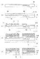
そして、図6〜図11は、6軸力センサ1が、上述した各々の力及びモーメントが与えられることによる変形を示している。
図6(a)は上方向から見た平面図であり、図6(b)は横方向から見た側面図である。
ここで、図6(a)は、力「−Fy」がY軸に沿って、図の上方向から下方向に向かって印加されていることを示している。
【0048】
力「−Fy」がY軸方向に印加されているため、連結部5B及び連結部5Dと作用部4との各々の接続部の部分に歪みが生じる。
このとき、抵抗素子Sxa3及びSxb1には、圧縮による歪みが発生して抵抗値が減少する。
また、抵抗素子Sxa1及びSxb3には、引っ張りによる歪みが発生して抵抗値が増加する。
【0049】
一方、連結部5A及び連結部5Cと作用部4との接合部には、弾性部5Ab及び弾性部5Cbに、力「−Fy」が吸収されることにより、歪みの発生が抑えられる。
これにより、連結部5A表面の抵抗素子Sya1〜Sya3,及び連結部5C表面の抵抗素子Syb1〜Syb3は抵抗の変化は極めて小さい。
図7(a)は上方向から見た平面図であり、図7(b)は横方向から見た側面図である。
ここで、図7(a)は、力「Fx」がX軸に沿って、図の左方向から右方向に向かって印加されていることを示している。
力「Fx」がX軸方向に印加されているため、連結部5A及び連結部5Cと作用部4との各々の接続部の部分に歪みが生じる。
【0050】
このとき、抵抗素子Sya3及びSyb1には、圧縮による歪みが発生して抵抗値が減少する。
また、抵抗素子Sya1及びSyb3には、引っ張りによる歪みが発生して抵抗値が増加する。
一方、連結部5B及び連結部5Dと作用部4との接合部には、弾性部5Bb及び弾性部5Dbに、力「Fx」が吸収されることにより、歪みの発生が抑えられる。
これにより、連結部5B表面の抵抗素子Sxa1〜Sxa3,及び連結部5D表面の抵抗素子Sxb1〜Sxb3は抵抗の変化は極めて小さい。
【0051】
また、図8(a)は上方向から見た平面図であり、図8(b)は横方向から見た側面図である。
ここで、図8(b)は、力「−Fz」がZ軸(図の平面に垂直)に沿って、図の上面方向から下面方向に向かって印加されていることを示している。
力FzがZ軸方向に印加されているため、連結部5A〜連結部5Dと作用部4との各々の接続部の部分に歪みが生じる。
このとき、抵抗素子Sxa1〜Sxa3,Sya1〜Sya3,Sxb1〜Sxb3,Syb1〜Syb3には、一様に圧縮による歪みが発生して抵抗値が減少する。
【0052】
また、図9(a)は上方向から見た平面図であり、図9(b)は横方向から見た側面図である。
ここで、図9(b)は、モーメントMyがY軸を回転軸として、矢印の方向へ印加されていることを示している。
モーメントMyがY軸を回転軸とした回転方向に印加されているため、連結部5B及び連結部5Dと作用部4との各々の接続部の部分に歪みが生じる。
このとき、抵抗素子Sxa1〜Sxa3には、圧縮による歪みが発生して抵抗値が減少する。
また、抵抗素子Sxb1〜Sxb3には、引っ張りによる歪みが発生して抵抗値が増加する。
【0053】
一方、連結部5A及び連結部5Cと作用部4との接合部には、弾性部5Ab及び弾性部5Cbに、モーメントMyが吸収されることにより、歪みの発生が抑えられる。
これにより、連結部5A表面の抵抗素子Sya1〜Sya3,及び連結部5C表面の抵抗素子Syb1〜Syb3は抵抗の変化は極めて小さい。
また、図10(a)は上方向から見た平面図であり、図10(b)は横方向から見た側面図である。
ここで、図10(b)は、モーメントMxがX軸を回転軸として、矢印の方向へ印加されていることを示している。
モーメントMxがX軸を回転軸とした回転方向に印加されているため、連結部5A及び連結部5Cと作用部4との各々の接続部の部分に歪みが生じる。
【0054】
このとき、抵抗素子Syb1〜Syb3には、圧縮による歪みが発生して抵抗値が減少する。
また、抵抗素子Sya1〜Sya3には、引っ張りによる歪みが発生して抵抗値が増加する。
一方、連結部5B及び連結部5Dと作用部4との接合部には、弾性部5Bb及び弾性部5Dbに、モーメントMxが吸収されることにより、歪みの発生が抑えられる。
これにより、連結部5B表面の抵抗素子Sxa1〜Sxa3,及び連結部5D表面の抵抗素子Sxb1〜Sxb3は抵抗の変化は極めて小さい。
【0055】
さらに、図11(a)は上方向から見た平面図であり、図11(b)は横方向から見た側面図である。
ここで、図11(a)は、モーメントMzがZ軸を回転軸として、反時計回りの方向へ印加されていることを示している。
モーメントMzがZ軸を回転軸として回転方向に印加されているため、連結部5A〜連結部5Dと作用部4との各々の接続部の部分に歪みが生じる。
このとき、抵抗素子Sya1,Sxb1,Syb1,Sxa1には、圧縮による歪みが発生して抵抗値が減少する。
また、抵抗素子Sya3,Sxb3,Syb3,Sxa3には、引っ張りによる歪みが発生して抵抗値が増加する。
【0056】
<試作した6軸力センサによる6軸力の測定>
次に、実際に作成した6軸力センサ1の概要を説明する。
以下に、試作した6軸力センサ1のプロセスパラメータを以下に示す。
半導体基板2は、P(燐)ドープのn型シリコン基板であり、抵抗率が1Ωcmである。
そして、半導体基板2は、n型(100)シリコン基板であり、各抵抗素子を構成するp型の活性層Sの長軸方向は<011>方向または<0−11>方向のいずれかに平行に形成されている。
なお、イオン注入により形成した活性層Sのシート抵抗(ρ□)は500[Ω/□]であり、上記試作した6軸力センサ1の各抵抗素子Sxa1〜Sxa3,Sya1〜Sya3,Sxb1〜Sxb3,Syb1〜Syb3は、53kΩの抵抗値として形成された。
【0057】
次に、図12は、一例として試作した6軸力センサ1の各部の形状及び寸法を示している。ここで、図12(a)〜(c)に示されている寸法は、全てmm単位である。
図12(a)は、上方から見た平面図であり、各部の寸法が示されている。
半導体基板2、すなわち6軸力センサ1のチップ寸法は10mm×10mmであり、作用部4の大きさは3mm×3mmである。
作用部4の各辺の中央から対向する支持部3の方向に、幅0.4mmで長さ1.325mmの橋梁部5Aa,5Ba,5Ca,5Daが形成されている。
【0058】
穴の領域A,B,C,Dは、幅0.2mmで長さ5.25mmの寸法において貫通して形成されている。
弾性部5Ab,5Bb,5Cb,5Dbは、幅0.2mmで長さ5.25mmの寸法において形成されており、各中央部分に、垂直にそれぞれ橋梁部5Aa,5Ba,5Ca,5Daの一端が接続されている。
【0059】
また、図12(b)は、抵抗素子Sxa1〜Sxa3,Sya1〜Sya3,Sxb1〜Sxb3,Syb1〜Syb3の形成される位置関係を示している。
例えば、橋梁部5Aaと作用部4との接続部に形成される抵抗素子Sya1〜Sya3を例として説明する。他の橋梁部と作用部4との接続部に形成される抵抗素子についても以下の説明と同様である。
抵抗素子Sya1〜Sya3は、幅0.07mm,ピッチ0.07mmにおいて、橋梁部5Aaと作用部4との接続部近傍に配置されている。
そして、各抵抗素子は、図12(c)に示すように、0.07mmの幅の領域に、0.01mmの幅の活性層Sが0.3mmの長さで、0.01mmのピッチで4本形成された構造となっている。
【0060】
図12(b)に戻り、抵抗素子Sya1〜Sya3は、橋梁部5Aaと作用部4との接続部において、橋梁部5Aaの長軸方向に活性層Sの長軸方向が平行となるように配置される。
また、抵抗素子Sya1〜Sya3は、各々の長軸方向の中央が作用部4の辺に対応する位置に配置されている(上記辺の上下0.15mmずつ形成されている)。
そして、抵抗素子Sya2は橋梁部5Aの短軸方向の中央部に配置されていて、抵抗素子Sya1,Sya3は抵抗素子Sya2の端部に対向していない外側の端部が、橋梁部5Aの短軸方法の各端部から0.025m離れる位置に形成されている。
【0061】
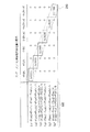
次に、すでに述べたプロセスパラメータと、図12に示した形状とにおいて試作された6軸力センサ1の印加される力とモーメントの各成分を検出するセンサ特性を示す。
図13には、作用部4に対して、印加される力及びモーメントと、単位(力またはモーメント)当たりの演算抵抗変化率との関係を示したテーブルが示されている。
左側の領域100には、作用部4に外力が印加された場合に得られる、力及びモーメントの6成分に対応した各抵抗値の抵抗変化率から、演算抵抗変化率を求める式が示されている。
【0062】
例えば、以下に示す(1)式によりX軸方向に印加される力Fxを算出するための演算抵抗変化率を求める。
Sig1 = ((R'Sya1-R'Sya3)+(R'Syb3-R'Syb1))/4 …(1)
同様に、以下に示す(2)〜(6)式により力Fy,Fz及びモーメントMx,My,Mzの各々を算出するための演算抵抗変化率を求める。
Sig2 = ((R'Sxa3-R'Sxa1)+(R'Sxb1-R'Sxb3))/4 …(2)
Sig3 = (R'Sxa2+R'Sya2+R'Sxb2+R'Syb2)/4 …(3)
Sig4 = (R'Sya2-R'Syb2)/2 …(4)
Sig5 = (R'Sxb2-R'Sxa2)/2 …(5)
Sig6 = ((R'Sxa3-R'Sxa1)+(R'Sya3-R'Sya1)+(R'Sxb3-R'Sxb1)
+(R'Syb3-R'Syb1))/8 …(6)
上記各式は、外力が印加されて、各々の橋梁部と作用部との接続部に発生する歪みにより、延ばされる(引張りを受ける)抵抗素子と圧縮される抵抗素子との抵抗変化率から構成されている。
例えば、R'Sya1は、抵抗素子Sya1の抵抗変化率である。
【0063】
ここで、図13のテーブルをみて判るように、各式は、テーブルの非対角成分が「0」、または対角成分200に比較して小さな数値となるように抵抗素子が選択されて用いられている。
すなわち、上記(1)式〜(6)式は、各軸の力又はモーメントを測定するとき、他軸干渉を防止するため、特定軸以外の力又はモーメントでの抵抗変化率が各々打ち消しあうように、抵抗素子を選択し、演算抵抗変化率の演算を行うように構成されている。
力Fxの印加に対応した(1)式に注目すると、Fxが与えられたとき、抵抗素子Sya1とSya3とに引張応力、抵抗素子Sya3とSya1に圧縮応力が印加されるので演算抵抗変化率は単位Fx当り0.00431(1/N)である。
【0064】
また、力Fxの印加に対応した(1)式に注目すると、Fyが与えられたとき、抵抗素子Sya1と抵抗素子Sya3とは双方ともに引張応力が印加され、抵抗素子Syb3と抵抗素子Syb1とは双方ともに圧縮応力が印加されることとなり、抵抗変化率R'Sya1とR'Sya3と、及び抵抗変化率R'Syb3とR'Syb1とが互いに相殺しあう(キャンセルしあう)こととなる。
したがって、Fyが与えられたとき、演算抵抗変化率Sig1は、(1)式において理論的に「0」として求められる。
また、(1)式において、Fzが印加されたとき、抵抗素子Sya1,Sya3,Syb3,Syb1のすべてに、引張応力が印加されることになり、やはり、抵抗変化率Sig1は、(1)式において理論的に「0」として求められる。
【0065】
さらに、(1)式において、Mxが印加されたとき、抵抗素子Sya1と抵抗素子Sya3とは双方ともに引張応力が印加され、抵抗素子Syb3と抵抗素子Syb1とは双方ともに圧縮応力が印加されることになり、演算抵抗変化率Sig1は、(1)式において理論的に「0」として求められる。
また、(1)式において、Myが印加されたとき、抵抗素子Sya1とSya3に圧縮応力、Sya3とSya1に引張応力がかかるため、演算抵抗変化率Sig1は、(1)式において理論的に「0」とならない。
しかしながら、弾性部5Ab,5Cbが歪みをある程度吸収するため、Fxの入力時の演算抵抗変化率の値と比較して小さな数値となる。
【0066】
さらに、(1)式において、Mzが印加されたとき、抵抗素子Sya1と抵抗素子Syb1とは双方ともに引張応力が印加され、抵抗素子Sya3と抵抗素子Syb3とは双方ともに圧縮応力が印加されることになり、これらの抵抗素子の抵抗変化率が(R'Sya1-R'Sya3)と(R'Syb3-R'Syb1)としてキャンセルし合うこととなり、演算抵抗変化率Sig1は、(1)式において理論的に「0」として求められる。
この結果から、逆行列を求めFxと演算抵抗変化の関係を求めると、上述したように、力Fxが、ほぼ「Fx=Sig1・[対角要素]11(従来例で示したm'11に対応)」の関係となる。
【0067】
このように、非対角要素の数値が「0」、または対角要素に比較して非常に小さな数値となるように、抵抗素子を選択し、これら抵抗素子の抵抗変化率から演算抵抗変化率Sig1を求める式とを形成しているので、他軸干渉の発生する可能性を大幅に低減できる。
他の(2)式〜(6)式も同様に、非対角要素が、「0」となるか、もしくは対角要素に対して小さな値となるように、測定に用いられる抵抗素子が選択されている。
上記各抵抗素子は、各橋梁部において、中央に配置された抵抗素子と、この抵抗素子の両側の対称的な位置に配置されているので、上述のような抵抗変化率のキャンセルが可能となっている。
ここで、各式において、式で使用した抵抗の数で除算しているのは、1本の抵抗の抵抗変化率として規格化するためである。
【0068】
上述した処理と同様に、(2)式〜(6)式により、各成分の力またはモーメントの印加に対する演算抵抗変化率を求めた結果が図13のテーブルである。
上述した(1)式〜(6)式において、抵抗変化率Sig1,2,3については1Nあたりの演算抵抗変化率として求め、演算抵抗変化率Sig4〜Sig6については1N・cmあたりの抵抗変化率として求める。
【0069】
ここで、各抵抗素子単体での抵抗変化率の求め方の説明を行う。
例えば、抵抗素子Sxa1の抵抗値をRsxa1(応力のかかった状態)として、その抵抗変化率をR'sxa1とし、補償抵抗である抵抗素子13の抵抗値をRcompとすると、真の抵抗素子Sxa1の抵抗値は、「Rsxa1・Rcomp(0)/Rcomp」である。
ここで、Rcomp(0)が室温での抵抗値であり、Rcompがそのときの周囲の温度に基づく抵抗値である。
そして、抵抗変化率R'sxa1は、以下に示す式により求められる。
R'sxa1=((Rsxa1・Rcomp(0)/Rcomp)−Sxa1(0))/Sxa1(0)
ここで、抵抗値Sxa1(0)は、抵抗素子Sxa1に対して応力がかかっていない状態の、抵抗素子Sxa1の抵抗値を示している。
他の抵抗素子Sxa2,3,Sxb1〜Sxb3,Sya1〜Sya3,Syb1〜Syb3の抵抗変化率R'Sxa2,3,R'Sxb1〜R'Sxb3,R'Sya1〜R'Sya3,R'Syb1〜R'Syb3も、上述した抵抗素子Sxa1の抵抗変化率R'sxa1と同様に求める。
また、上記各抵抗値は、信号電極10で測定される電流−電圧特性により求められる。
【0070】
次に、測定から得られた、力又はモーメントの単位あたりの演算抵抗変化率を示す図13のテーブルに基づいて、本発明の6軸力センサ1で測定される演算抵抗変化率から印加された外力の力及びモーメントを求める、以下に示す(7)式を作成する。
【数1】

すなわち、上記逆行列が各軸毎に演算抵抗変化率と力又はモーメントとの関係を求めるマトリクスとなり、(7)式に演算抵抗変化率を与えることで、力及びモーメントの成分が求められる。
【0071】
ここで、(7)式の右辺のマトリクスにおける非対角要素は、対角要素の数値に比較して小さい値、または「0」であるため、各軸の他軸干渉を抑制することが可能となる。
すなわち、力Fxを与えた場合(他の力及びモーメントも同様である)に、力Fxの数値のみが(1)式の演算結果として得られるように、他軸干渉を抑制する抵抗変化率−力及びモーメントの関係を示すマトリクスを構成することができる。
上述したように、他軸干渉により測定値の再現性に問題が生じやすい従来例と比較して、本発明の6軸力センサは、非対角成分を「0」もしくは対角成分に比較して非常に小さな数値とする演算抵抗変化率−力及びモーメントの関係を示すマトリクスを得ることができ、他軸干渉を抑制することとなり、測定値の再現性及びロバスト性を向上することが可能となる。
【0072】
次に、上述してきたように半導体基板2の表面だけでなく裏面にも、抵抗素子を形成した場合の測定について、試作した6軸力センサを用いて、以下に説明する。
図14に裏面に作成した各抵抗素子の位置関係を示す。図14は、半導体基板2の上面(すでに説明した半導体素子の形成された表面)から、下部を透視した図であり、例えば、抵抗素子Sya1の裏側には抵抗素子Sya1uが形成されており、抵抗素子Syb1の裏側には抵抗素子Syb1uが形成されている。
これらの、製造方法はすでに述べた表面における各抵抗素子の製造方法と同様である。
すなわち、表面の各抵抗素子を作成した後、表面を何らかの材料により覆って保護した後、裏面に対して表面と同様なプロセスにより各半導体素子を形成して、表面の保護に用いた材料を除去して作成する。
【0073】
A.裏面の4個の抵抗素子を用いた場合
図13のテーブルで説明した方法と同様に、図15のテーブルの対角要素210の各対角要素を、以下に示す(8)式〜(13)式(図16の領域110に記載される)に基づき求める。
この図15のテーブル作成においては、表面の抵抗素子全てと、連結部5Aの抵抗素子Sya2u,連結部5Bの抵抗素子Sxa2u,連結部5Cの抵抗素子Syb2u,連結部5Dの抵抗素子Sxb2uを用いている。
【0074】
このとき、図14には12本の抵抗素子が示されているが、図15のテーブル作成においては、6軸力センサにおいて抵抗素子Sya2u,Sxa2u,Syb2u,Sxb2uのみを図14に記載した位置に配置する構造となる。
Sig1 = ((R'Sxb2+R'Sxb2u)-(R'Sxa2+R'Sxa2u))/4 …(8)
Sig2 = ((R'Syb2+R'Syb2u)-(R'Sya2-R'Sya2y))/4 …(9)
Sig3 = ((R'Sxa2-R'Sxa2u)+(R'Sya2-R'Sya2u)+(R'Sxb2-R'Sxb2u)
+(R'Syb2-R'Syb2u))/8 …(10)
Sig4 = ((R'Sya2-R'Sya2u)-(R'Syb2-R'Syb2u))/4 …(11)
Sig5 = ((R'Sxb2-R'Sxb2u)-(R'Sxa2-R'Sxa2u))/4 …(12)
Sig6 = ((R'Sxa3-R'Sxa1)+(R'Sya3-R'Sya1)+(R'Sxb3-R'Sxb1)
+(R'Syb3-R'Syb1))/8 …(13)
ここで、力及びモーメントの各成分あたりの演算抵抗変化率Sig1〜Sig6を求める場合に、(1)式〜(6)式の場合と同様に、上記(8)式〜(13)式において、他軸干渉が起こらない抵抗素子の組み合わせを行う。
抵抗素子を6軸力センサ1の表面に配置したのみでは、図13のテーブルで見られるように、非対角要素をすべて「0」とすることができなかったが、裏面に配置した抵抗素子を用いることにより、図15に示すように、非対角要素をすべて「0」とするような(8)式〜(13)式を構成する抵抗素子の組み合わせが可能となる。
【0075】
例えば、作用部4に力Fxを印加した場合、演算抵抗変化率Sig1を求める(8)式は、表面及び裏面で対向する抵抗素子Sxb2及びSxa2と、抵抗素子Sxb2u及びSxa2uとの組み合わせで、抵抗素子1個あたりの演算抵抗変化率を求めている。
作用部4に対して、力Fxが印加されることにより、抵抗素子Sxb2,Sxb2uにはわずかであるが引っ張りの力がかかり、抵抗素子Sxa2,Sxa2uにはわずかであるが圧縮の力がかかる。
【0076】
例えば、力Myが印加されたとき、表面の抵抗素子だけの場合には、図13のようにFxを検知させたい演算抵抗変化率Sig1に、非常に小さい値ながら他軸干渉としての数値が現れる。
しかしながら、裏面に抵抗素子を配置して、適切な抵抗素子を選択して、この抵抗素子の抵抗変化率に基づく(8)式を用いて演算抵抗変化率Sig1を演算するならば、力Myのときに、抵抗変化率R'Sxb2とR'Sxb2uとがキャンセルしあい、かつ抵抗変化率R'Sxa2とR'Sxa2uとがキャンセルしあうこととなる。
したがって、モーメントMyに対して、非対角要素となる演算抵抗変化率Sig1の数値は「0」となる。
【0077】
そして、(7)式を求めたときと同様に、図15のテーブルを行列として、この逆行列を求めることで、演算抵抗変化率−力及びモーメントの関係を示すマトリクスを求める。
そして、この演算抵抗変化率−力及びモーメントの関係のマトリクスに基づき、以下に示す演算抵抗変化率−力及びモーメントの関係式である(14)式を作成する。
【数2】
【0078】
(14)式の右辺の抵抗変化率−力及びモーメントの関係のマトリクスをみて判るように、非対角要素がすべて「0」となっており、計算が簡単になるとともに、他軸干渉が大幅に抑制することができ、測定値の再現性及びロバスト性が向上するとともに、測定感度及び測定精度が向上する。
ここで、(7)式のマトリクスに比較して、(14)式の対角要素の数値の大きさが異なるが、実験上での数値であり、本発明の6軸力センサは、基板の厚さ,橋梁部の太さ,抵抗の配置の調整により、いかようにも数値の調整が可能であり、測定感度の調整は用途によって、かつ軸方向によっても適時変更することが可能である。
【0079】
B.裏面の12個の抵抗素子を用いた場合
図13のテーブルで説明した方法と同様に、図16のテーブルの対角要素220の各対角要素を、以下に示す(15)式〜(20)式(図16の領域120に記載される)に基づき求める。
この図16のテーブル作成においては、表面の抵抗素子全てと、図13に示す裏面の連結部5Aの抵抗素子Sya1u〜Sya3u,連結部5Bの抵抗素子Sxa1u〜Sxa3u,連結部5Cの抵抗素子Syb1u〜Syb1u,連結部5Bの抵抗素子Sxb1u〜Sxb3uの12個全てとを用いている。
Sig1 = ((R'Sya1-R'Sya3)+(R'Syb3-R'Syb1)+(R'Sya1u-R'Sya3u)
+(R'Syb3u-R'Syb1u))/8 …(15)
Sig2 = ((R'Sxa3-R'Sxa1)+(R'Sxb1-R'Sxb3)+(R'Sxa3u-R'Sxa1u)
+(R'Sxb1u-R'Sxb3u))/8 …(16)
Sig3 = ((R'Sxa2-R'Sxa2u)+(R'Sya2-R'Sya2u)+(R'Sxb2-R'Sxb2u)
+(R'Syb2-R'Syb2u))/8 …(17
Sig4 = ((R'Sya2-R'Sya2u)-(R'Syb2-R'Syb2u))/4 …(18)
Sig5 = ((R'Sxb2-R'Sxb2u)-(R'Sxa2-R'Sxa2u))/4 …(19)
Sig6 = ((R'Sxa3-R'Sxa1)+(R'Sya3-R'Sya1)+(R'Sxb3-R'Sxb1)
+(R'Syb3-R'Syb1)+(R'Sxa3u-R'Sxa1u)+(R'Sya3u-R'Sya1u)
+(R'Sxb3u-R'Sxb1u)+(R'Syb3u-R'Syb1u))/16 …(20)
ここで、力及びモーメントの各成分あたりの演算抵抗変化率Sig1〜Sig6を求める場合に、(1)式〜(6)式,及び(8)式〜(13)の場合と同様に、上記(15)式〜(20)式において、他軸干渉が起こらない抵抗素子の組み合わせを行う。
【0080】
抵抗素子を6軸力センサ1の表面に配置したのみでは、図13のテーブルで見られるように、非対角要素をすべて「0」とすることができなかったが、図16に示すように、図15と同様に非対角要素をすべて「0」とするような(15)式〜(20)式を構成する抵抗素子の組み合わせが可能となる。
そして、対角要素220における抵抗素子Sya1,Sya2に対応する値を図15のテーブルに比較して、大きくすることができ、力Fx,Fy検出感度を向上させることが可能となる。
【0081】
例えば、作用部4に力Fxを印加した場合、変化量Sig1を求める(15)式は、表面及び裏面で対向する抵抗素子Sya1,Sya3,Syb1及びSyb3と、抵抗素子Sya1u,Sya3u,Syb1u及びSyb3uとの組み合わせで、抵抗素子1本あたりの演算抵抗変化率を求めている。
作用部4に対して、力Fxが印加されることにより、抵抗素子Sya1,Syb3,Sya1u,Syb3uには引っ張りの力がかかり、抵抗素子Sya3,Syb1,Sya3u,Syb1uには圧縮の力がかかる。
【0082】
このとき、(8)及び(9)式の様に、弾性部により、力Fxが吸収されてしまう部分の抵抗素子を使用していないため、測定感度を低下させることなく、印加される外力を力及びモーメントの成分に分離することが可能であり、印加される外力の測定精度及び測定感度を向上させることが可能である。
そして、(7)式を求めたときと同様に、図16のテーブルを行列として、この逆行列を求めることで、抵抗変化率−力及びモーメントの関係を示すマトリクスを求める。
そして、この抵抗変化率−力及びモーメントの関係のマトリクスに基づき、以下に示す抵抗変化率−力及びモーメントの関係式である(21)式を作成する。
【数3】
【0083】
(21)式の右辺の演算抵抗変化率−力及びモーメントの関係のマトリクスをみて判るように、非対角要素がすべて「0」となっており、他軸干渉が大幅に抑制されるため、測定値の再現性及びロバスト性が向上し、かつ(14)式に比較して対角要素の数値が同様となるため、測定感度及び測定精度がさらに向上する。
また、本発明の6軸力センサは、基板の厚さ,橋梁部の太さ,抵抗の配置の調整により、いかようにも数値の調整が可能であり、測定感度の調整は用途によって、かつ軸方向によっても適時変更することが可能である。
【0084】
プロセスパラメータ及び6軸力センサの形状及び各部の寸法は、使用用途などにより適時最適化されるものであり、上述してきた各種数値は一例を示したものに過ぎない。
【0085】
以上、本発明の一実施形態を図面を参照して詳述してきたが、具体的な構成はこの実施形態に限られるものではなく、本発明の要旨を逸脱しない範囲の設計変更等があっても本発明に含まれる。
上述の一実施形態において、各半導体抵抗の配置については、一例を示したに過ぎず、他軸干渉を防止するため、演算抵抗変化率−力及びモーメントの関係を示すマトリクスにおいて、非対角成分を、キャンセルできる抵抗素子の組み合わせと、(1)〜(6),(8)〜(13),(15)〜(20)式等のように、力及びモーメントの成分に対応する演算抵抗変化率の演算式が求められれば、同様の効果を得ることが可能である。
【0086】
また、一実施形態では、6軸力センサは、n型の半導体基板2が結晶方向(100)面であり、p型の活性層Sよりなる各半導体抵抗素子の電流軸が<011>または<0−11>方向で配置した構造で説明した。
しかし、本発明の6軸力センサは、結晶方向が(110)面の半導体基板2を用い、p型の活性層Sよりなる各半導体抵抗素子を電流軸が<1−10>または<00−1>方向となるように配置してもよい。
また、本発明の6軸力センサは、結晶方向が(110)面の半導体基板2を用い、p型の活性層Sよりなる各半導体抵抗素子の電流軸が<1−1−1>または<−11−2>方向となるように配置してもよい
上述した結晶方向及び電流軸の組み合わせにより、同様な歪みに対して、より大きな抵抗変化を得ることができ、印加される外力の力及びモーメントの成分の測定精度を向上させることが可能となる。
【0087】
さらに、本発明の他の実施形態として、図17に示す構造の6軸力センサにおいても、一実施形態と同様の効果を得ることが可能である。
図17は、他の実施形態による6軸力センサ300の構造を示した上面から見た平面図である。
この6軸センサ300は、穴の領域301〜304,支持部305,作用部306,弾性部307,308,309,310,橋梁部311,312,313,314から構成されている。
【0088】
抵抗素子の配置形状及び数は一実施形態と同様であり、演算抵抗変化率と力及びモーメントの各成分との求め方も一実施形態と同様である。
一実施形態と異なっている点は、穴の領域K,L,M,Nに対応する構成が無く、弾性部307,308,309,310の部分の剛性が低くなるように薄く形成されている点であり、他の構成は同様である。
そして、支持部305の部分において、支持台に固定した場合、弾性部307,308,309,310が、一実施形態の弾性部5Ab,5Bb,5Cb,5Dbと同様に弾性体として働くことになる。
【0089】
【発明の効果】
本発明の6軸力センサによれば、半導体基板からなる6軸力センサ機能を有するセンサチップであり、該センサチップが、外力が印加される作用部と、
外部構造体に固定する支持部と、前記作用部と前記支持部とを連結する、剛性の高い領域と剛性の低い領域とからなる連結部とから構成され、前記連結部の表面に、活性層で形成された半導体抵抗素子が配置され、各々の半導体抵抗素子が支持部の各辺に対向する電極に配線されている構成であるため、剛性の低い領域が連結部にかかる余分な歪みを吸収する機能を有し、センサチップ全体の歪みを抑制し、各々の半導体抵抗素子に対して選択的に、印加される力及びモーメント成分による歪みを発生させることができ、他軸干渉が抑制されるように、各軸にかかる力またはモーメントの測定値を求めるために使用する半導体抵抗素子の組み合わせを選択し、演算抵抗変化率を求める式を効果的に構成することが可能となるため、作用部に加えられる外力を力及びモーメントの6成分に分離でき、力及びモーメントの測定の再現性及びロバスト性を向上させることができる。
これにより、本発明の6軸力センサは、各連結部毎の各半導体抵抗素子の抵抗変化から求められる電気信号に、予期しない外乱などによるノイズが重畳したとしても、上述したように、測定に用いる半導体抵抗素子の組み合わせにより、他軸の干渉を受けずに、作用部に印加される外力を、力及びモーメント成分に分離して測定することが可能なため、測定精度及び測定感度を向上させることが可能となる。
【図面の簡単な説明】
【図1】 本発明の一実施形態による6軸力センサ1の構造を示した上面から見た平面図である。
【図2】 図1の連結部5C周辺の拡大図である。
【図3】 図1に示す6軸力センサ1の製造プロセスをプロセス単位ごとの断面図である。
【図4】 作用部4に対して、各軸方向の力及びモーメントを示す符号の説明を行う概念図である。
【図5】 図1における連結部5A〜5C表面に形成された抵抗の位置関係を示す表面配置図である。
【図6】 6軸力センサ1が、作用部4に対して各軸の力又はモーメントが与えられることによる変形を示す概念図である。
【図7】 6軸力センサ1が、作用部4に対して各軸の力又はモーメントが与えられることによる変形を示す概念図である。
【図8】 6軸力センサ1が、作用部4に対して各軸の力又はモーメントが与えられることによる変形を示す概念図である。
【図9】 6軸力センサ1が、作用部4に対して各軸の力又はモーメントが与えられることによる変形を示す概念図である。
【図10】 6軸力センサ1が、作用部4に対して各軸の力又はモーメントが与えられることによる変形を示す概念図である。
【図11】 6軸力センサ1が、作用部4に対して各軸の力又はモーメントが与えられることによる変形を示す概念図である。
【図12】 一例として試作した6軸力センサ1の各部の形状及び寸法を示す寸法図である。
【図13】 作用部4に対して、各軸方向に印加される力及びモーメントと、単位当たりの演算抵抗変化率との関係を示したテーブルが示されている。
【図14】 半導体基板2の裏面に形成された抵抗素子の配置関係を示す透視図である。
【図15】 作用部4に対して、各軸方向に印加される力及びモーメントと、単位当たりの抵抗の変化量との関係を示したテーブルが示されている。
【図16】 作用部4に対して、各軸方向に印加される力及びモーメントと、単位当たりの抵抗の変化量との関係を示したテーブルが示されている。
【図17】 本発明の他の実施形態による6軸力センサ300の構造を示した上面から見た平面図である。
【符号の説明】
1,300 6軸力センサ
2 半導体基板
3,305 支持部
4,306 作用部
5A,5B,5C,5D 連結部
5Aa,5Ba,5Ca,5Da 橋梁部
5Ab,5Bb,5Cb,5Db 弾性部
307,308,309,310 弾性部
311,312,313,314 橋梁部
7 GND配線
8 信号配線
9 信号電極
10 信号電極
11 GND電極
12 バイアス電極
13 抵抗素子
301,302,303,304 穴の領域
A,B,C,D,K,L,M,N 穴の領域
Sxa1,Sxa2,Sxa3,Sya1,Sya2,Sya3 抵抗素子
Sxb1,Sxb2,Sxb3,Syb1,Syb2,Syb3 抵抗素子
Sxa1u,Sxa2u,Sxa3u,Sya1u,Sya2u,Sya3u 抵抗素子
Sxb1u,Sxb2u,Sxb3u,Syb1u,Syb2u,Syb3u 抵抗素子[0001]
BACKGROUND OF THE INVENTION
The present invention relates to a force sensor using a semiconductor resistance element, and relates to a small and highly accurate force sensor capable of detecting six components of force and moment.
[0002]
[Prior art]
In recent years, robots and manipulators are frequently used in machine tools, etc., and in order to respond to the miniaturization of objects, the need for high-precision multi-axis force sensors used as force sensors for robots and man-machine interfaces The nature is increasing.
A multi-axis force sensor is a strain-generating body that is elastically deformed when an external force is applied, and a strain resistance element whose electrical resistance changes due to mechanical deformation is arranged, and the resistance change of these resistance elements is taken out as an electrical signal. Based on this electric signal, the strength of the force of two or more components (for example, the X-axis direction and the Y-axis direction) applied to the strain generating body is detected.
[0003]
However, in the above-described conventional example, a plurality of strain gauges (the strain resistance elements and the like) are individually attached to the strain generating body independently. From each strain gauge, it is difficult to obtain an electric signal having a voltage level assumed for the degree of strain.
For this reason, in the above conventional example, due to the accuracy of the mounting position, it is difficult to ensure detection accuracy, and it is difficult to produce a multi-axis force sensor having the same characteristics with high reproducibility.
[0004]
Furthermore, in the above conventional example, it is necessary to apply a plurality of strain gauges with high positional accuracy, so that the application process takes time, productivity cannot be improved, and downsizing is difficult. There is.
[0005]
In addition, in the above conventional example, when the thermal expansion coefficient between the applied strain gauge and the strained body is greatly different due to repeated application of impact load, the strain from the strained body over time due to temperature stress. There is a problem that peeling of the gauge occurs, and the strain of the strain generating body is not sufficiently transmitted to the strain gauge, so that an accurate electrical signal is not output from the strain gauge and accurate measurement cannot be performed.
[0006]
As a multi-axis force sensor that solves the problems of the conventional example described above, a semiconductor process is used to create a plurality of semiconductor resistance elements on a semiconductor single crystal substrate, thereby eliminating the need to attach a strain gauge to the strain generating body. Thus, there has been proposed a configuration that solves the problem of accuracy of the process of attaching the semiconductor resistance element to the strain generating body and enables miniaturization (Japanese Patent No. 2746298, Japanese Patent Publication No. 7-93445).
[0007]
[Problems to be solved by the invention]
However, in the multi-axis force sensor using the above-described semiconductor process, the entire substrate is isotropically distorted with respect to the application of a force or moment in each axial direction, and the arrangement of each semiconductor resistance element is not appropriate. Therefore, it is difficult to accurately separate external force applied from an unknown direction into each component.
That is, the component of the other axis is superimposed on the electric signal component detected from the resistance element corresponding to each component, and the measurement sensitivity of each component of force or moment is lowered.
[0008]
In general, in the case of a multi-axis force sensor, in order to obtain each component, a matrix indicating the relationship between the force or moment of each component and the resistance change rate is required.
The case of a six-axis force sensor will be described as an example in more detail. In the six-axis force sensor, the forces Fx, Fy, and Fz in the orthogonal x-axis, y-axis, and z-axis directions and the moments Mx, My, and Mz in the x-axis, y-axis, and z-axis can be obtained. . These are the forces F1, F2, F3, F4, F5 and F6, respectively.
The calculated resistance change rates obtained from the resistance change rates of the respective semiconductor resistance elements arranged in the 6-axis force sensor are S1, S2, S3, S4, S5, and S6.
[0009]
And between the calculation resistance change rate Si and the force Fi (i is an integer of 1 to 6),
(Si) = (mij) * (Fi) (j is an integer of 1 to 6)
Relationship, ie
S1 = m11 · F1 + m12 · F2 + m13 · F3 + m14 · F4 + m15 · F5 + m16 · F6
S2 = m21 ・ F1 + m22 ・ F2 + m23 ・ F3 + m24 ・ F4 + m25 ・ F5 + m26 ・ F6 ……
S6 = m61 · F1 + m62 · F2 + m63 · F3 + m64 · F4 + m65 · F5 + m66 · F6
There is a relationship.
Here, (Si) and (Fi) are i-row matrices, and (mij) is an i-row and j-column matrix.
[0010]
Each matrix element mij of the matrix (mij) can be obtained in advance by obtaining the above-described calculation resistance change rates with respect to only a single component input.
And by calculating the inverse matrix (m′ij) of this matrix (mij),
(Fi) = (m′ij) × (Si)
Matrix computation of
F1 = m'11, S1 + m'12, S2 + m'13, S3 + m'14, S4 + m'15, S5 + m'16, S6
F2 = m'21, S1 + m'22, S2 + m'23, S3 + m'24, S4 + m'25, S5 + m'26, S6
......
F6 = m'61, S1 + m'62, S2 + m'63, S3 + m'64, S4 + m'65, S5 + m'66, S6
As a relation, the force and moment in each axial direction can be obtained based on the calculated resistance change rate obtained from the resistance change rate of each semiconductor resistance element.
In each of the above equations, if the numerical value of the matrix element mij is large, for example, if the resistance change rate Si fluctuates due to the weight of noise, the influence appears on the measured values of F1 to F6.
[0011]
That is, there is a possibility that a measurement result does not become “0” due to a disturbance such as noise even though the input of other components is “0” when only a single component is input as an external force. Becomes higher.
Hereinafter, as described above, the fact that the measured value of the force or moment of the component to be obtained varies depending on the force or moment of the other axis is defined as occurrence of other axis interference.
Ideally, in the matrix (m′ij), the non-diagonal elements other than the diagonal elements m′11, m′22, m′33, m′44, m′55, and m′66 are set to “0”. The matrix (m′ij) is a diagonal matrix, and the relationship between each component of force or moment and the calculated resistance change rate is
F1 = m'11 ・ S1
F2 = m'22 ・ S2
......
F6 = m'66 ・ S6
If a function like this can be made, the calculation can be simplified and interference with other axes can be prevented.
[0012]
Actually, even if the non-diagonal element cannot be set to “0”, the influence of the other-axis interference can be reduced by making the value of the non-diagonal element very small compared to the diagonal element.
However, in the multiaxial force sensor having a structure in which the entire substrate is distorted and the arrangement of the semiconductor resistance elements is not considered as in the conventional example, the non-diagonal elements of the matrix (m′ij) are set to “0”, Alternatively, it cannot be made smaller than the diagonal element, and it is considered that the possibility of other-axis interference occurring increases.
That is, the conventional multi-axis force sensor is prone to other-axis interference, and noise due to unexpected disturbance is superimposed on the electrical signal from the semiconductor resistance element, resulting in a large measurement result due to other-axis interference. There is a high possibility that it will fluctuate.
Therefore, even when the multi-axis force sensor is used for a robot or the like, the measured value varies due to interference with other axes depending on the installation state, and there is a problem in reproducibility and robustness when used as a general-purpose part. is there.
[0013]
In order to solve the disadvantages of the multi-axis force sensor using the semiconductor process described above, a structure for separating the strain component for each axis has been proposed (Japanese Patent Laid-Open No. 11-333765).
Although this multi-axis force sensor is improved with respect to the sensor already described, this multi-axis force sensor is configured to detect force in the direction of three axes (x-axis, y-axis, z-axis), and is a six-axis force sensor. When used as, the separation function of each component is insufficient, and the problem of other-axis interference is not improved.
[0014]
The present invention has been made under such a background. The purpose of the present invention is to provide robustness and reproducibility that can suppress interference with other axes and detect the force or moment of each axis component in detecting the applied external force. It is to provide an improved 6-axis force sensor.
[0015]
[Means for Solving the Problems]
Of the present invention Many The axial force sensor (for example, the six-axis force sensor 1 in one embodiment) includes a semiconductor substrate (for example, the
[0016]
Of the present invention Many The axial force sensor element is formed in a region where a large strain is generated on the surface of the bridge portion when an external force is applied to the action portion as compared with other regions of the action portion or the connection portion. Distortion detection By arranging the elements, Distortion detection The element can selectively detect the force or moment of the desired component and Distortion detection Elemental Sensitivity (If the strain detection element is a semiconductor resistance element, the amount of change in resistance) The measurement sensitivity of the force and moment of the external force applied to the action part can be improved, and the robustness and stability in the measurement result can be obtained.
[0017]
Of the present invention Many The axial force sensor element is Distortion detection By disposing the element on the surface in the vicinity of the connection portion between the action portion and the bridge portion, the element is disposed in a region where the strain generated by the external force is most concentrated. Distortion detection It is possible to increase the amount of change in the resistance value of the element, effectively improve the measurement sensitivity of the force and moment of the external force applied to the action part, and obtain robustness and stability in the measurement result. .
[0018]
Of the present invention Many The axial force sensor element is Distortion detection By arranging the element in the constricted portion formed in the bridge portion, the stress generated in the constricted portion becomes the largest in the connecting portion corresponding to each component of the force or moment of the external force applied to the action portion. Therefore, the strain is concentrated most in this constricted part, and against the external force Distortion detection It is possible to increase the resistance change of the element, effectively improve the measurement sensitivity of the force and moment of the external force applied to the action part, and obtain robustness and stability in the measurement result.
[0019]
Of the present invention Many The axial force sensor element is Distortion detection By disposing a plurality of elements in parallel to the major axis direction for each bridge portion, a plurality of elements are provided. Distortion detection It becomes possible to take out electrical signals by combining the resistance change rates obtained from the elements, so as to prevent other-axis interference, that is, the resistance change rates for other than forces or moments in a specific direction cancel each other. Distortion detection Select elements, and these Distortion detection An equation suitable for obtaining six components of force and moment can be constructed from the resistance change rate of the element, and a non-diagonal element in a matrix indicating the relationship between the force and moment and the resistance change rate based on this equation. Can be “0” or sufficiently small. As a result, the present invention Many The axial force sensor can suppress interference from other axes, and the force and moment of the applied external force. Many The measurement accuracy of components can be improved, and the robustness in the measurement results of force and moment can be improved.
[0020]
Of the present invention Many In the axial force sensor element, the inner corners of the connection part of the connection part and the action part, the connection part of the connection part and the support part, and the connection part of the elastic part and the bridge part are arc-shaped (for example, , In one embodiment, it is processed and formed on the inner periphery of the hole regions A, B, C, D, K, L, M, and N), so that the stress at each connection portion is reduced. In order to suppress the concentration of stress on the inner corner portion and improve the structural strength with respect to the external force applied to the acting portion by dispersion, it is possible to widen the measurement range of the applied external force.
[0021]
Of the present invention Many In the axial force sensor element, a semiconductor resistance element for temperature compensation (for example, the
[0022]
Of the present invention Many The axial force sensor element has a guard wiring that is a ground potential (for example, the
[0023]
Of the present invention Many The axial force sensor element is formed with a bias electrode (for example, the
[0024]
Of the present invention Many In the semiconductor substrate, the axial force sensor element is the bridge portion. Distortion detection At least one or more in the region of the back surface opposite to the region where the element is arranged Distortion detection Elements (for example, resistance elements Sya1u to Sya3u, Sxa1u to Sxa3u, resistance elements Syb1u to Syb1u, Sxb1u to Sxb3u in one embodiment) are formed in parallel to the major axis direction of the bridge portion and are connected to electrodes by wiring Each formed on the front and back surfaces. Distortion detection Based on the resistance change of the element, the force and moment of the external force applied to the action part are applied only to the surface. Distortion detection Compared with the case where an element is provided, it is possible to measure with high accuracy by separating each specific component, and it is possible to obtain robustness and stability in the measurement result.
[0025]
DETAILED DESCRIPTION OF THE INVENTION
Hereinafter, embodiments of the present invention will be described with reference to the drawings.
<Structure and function of 6-axis force sensor>
FIG. 1 is a plan view seen from above showing a structural example of a six-axis force sensor according to an embodiment of the present invention. In this figure, a six-axis force sensor 1 includes resistance elements (piezoresistive elements) Sxa1 to Sxa3, Sxb1 to Sxb3, Sya1 to Sya3, Syb1 to Syb3 made of an active layer (diffusion layer) formed on the upper surface of a
The
Here, the inner corners in the inner periphery of the hole regions A, B, C, D, K, L, M, and N are processed into an arc shape, preferably R processed.
[0026]
That is, the six-axis force sensor 1 is functionally separated into a plurality of regions by the regions A, B, C, D, K, L, M, and N, and the outer peripheral portion of the
The
The connecting
[0027]
The elastic portions 5Ab, 5Bb, 5Cb, and 5Db are formed so as to be respectively connected to the support portion 3 at two ends in the major axis direction around the regions A, B, C, and D, respectively. .
And as for bridge part 5Aa, 5Ba, 5Ca, 5Da, one edge part in a major axis direction is connected to the
Here, the connecting portions of the bridge portions 5Aa, 5Ba, 5Ca, 5Da, the elastic portions 5Ab, 5Bb, 5Cb, 5Db and the
Further, in the structure example of FIG. 1, in the
[0028]
The resistance elements Sya1, Sya2, and Sya3 are formed in the connecting
The resistance elements Sya1, Sya2, and Sya3 are formed so as to be parallel to the major axis direction of the bridge portion 5Aa.
The other resistance elements Syb1 to Syb3, resistance elements Sxa1 to Sxa3, and resistance elements Sxb1 to Sxb3 are also supported by the
[0029]
That is, in FIG. 2 (enlarged view around the connecting portion 5C in FIG. 1), a resistance element Syb1 composed of the active layer S in the major axis direction of the bridge portion 5Ca is located in the vicinity of the connecting portion between the connecting portion 5C and the
The positional relationship between the resistance elements Syb1 to Syb3 is that the resistance element Syb2 is arranged at the center of the bridge portion 5Ca (center line of the action portion 4), and the resistance elements Syb1 and Syb3 are located on both sides of the resistance element Syb2 in the bridge portion 5Ca. They are arranged at symmetrical positions.
Here, each active layer S is formed so as to be folded back multiple times to increase the overall length in order to form a resistive element in a compact manner, but is not limited to this shape.
Further, the
[0030]
The
When the
Regardless of whether or not the
[0031]
Here, the
Therefore, when the current from each resistance element is detected by separating each resistance element and each
In this embodiment, one of the resistance elements is connected to the ground potential. However, depending on the measurement method, it may not be connected to the ground potential.
When this connection is not made, it is necessary to provide another GND wiring dedicated to the guard separately from each signal wiring of each resistance element, and to connect these other GND wirings independently to the ground potential.
[0032]
Returning to FIG. 1, the GND wirings 7 are each connected to a
Each of the
The
Further, each of the
These
With these measuring instruments or analysis devices, the resistance value is measured from the current-voltage characteristics, and the resistance change rate of each resistance element based on the applied external force is obtained.
[0033]
The
Due to the bias voltage applied via the bias electrode, a depletion layer grows at the interface of the active layer S (see FIG. 2), and insulation between the active layer S and the
[0034]
The
A predetermined voltage is applied to the
That is, based on the resistance change of the
[0035]
As described above, the 6-axis force sensor 1 according to the present invention includes the
Here, the connecting
[0036]
For this reason, the 6-axis force sensor 1 according to the present invention has the elastic portions 5Ab, 5Ab, and 5Aa when the external elements applied to the
[0037]
<Manufacturing method of 6-axis force sensor>
Next, an example of a method for manufacturing the six-axis force sensor 1 will be described with reference to FIG.
FIG. 3 is a cross-sectional view for each predetermined process unit for explaining the manufacturing process of the six-axis force sensor 1.
In FIG. 3A, boron, which is a p-type impurity, is formed on a
The resistive elements are resistive elements Sya1 to Sya3, Syb1 to Syb3, Sxa1 to Sxa3, Sxb1 to Sxb3, 13.
[0038]
Next, the resist pattern is removed, and a silicon oxide film is grown as an
Then, the
Here, the thickness of the
Further, the resistance value of the formed resistance element is 53 kΩ.
[0039]
Next, in FIG. 3B, a resist pattern (not shown) for forming a contact hole is formed, and using this resist pattern as a mask, the
Then, the resist pattern is removed, and Al—Si (alloy of aluminum and silicon) is sputtered on the entire surface of the
As a result, the contact CN between the
[0040]
Next, in FIG. 3C, a resist pattern (not shown) for forming regions of the
Further, the resist pattern is removed, and a SiN film (silicon nitride film) is formed as a passivation film by p-CVD (plasma chemical vapor deposition).
[0041]
Then, a resist pattern (not shown) for forming a bonding pad is formed, and the SiN film in a region to be an opening of the
Next, in FIG. 3 (d), formation of hole regions A, B, C, D, K, L, M, and N penetrating in the thickness direction in FIG. 1 and formation of resist patterns for chip division are performed. To do.
Then, the
[0042]
Next, in FIG. 3E, the opening of the resist pattern is removed by etching by RIE (reactive ion etching), and a through region, that is, regions A, B, C, D, K, L, M, and N hole regions are formed, and chip division (cutting out each chip from the wafer) is performed.
Then, the resist pattern is removed with an organic solvent, and the wax is melted and separated from the
Further, final cleaning is performed to complete the six-axis force sensor 1.
[0043]
In the above process, the impurity is introduced into the
Further, although the sputtering method is adopted as the metal film deposition method, an evaporation method assuming lift-off may be used.
[0044]
As described above, the 6-axis force sensor according to the present invention forms a semiconductor resistance element for detecting strain using a photolithography process on the surface of a semiconductor substrate, so that the element is accurately arranged at a desired position. Therefore, it is easy to manufacture an element having the performance as designed with good reproducibility, and productivity is improved.
Therefore, the present invention is easy to downsize and is excellent in reproducibility and productivity as compared with a conventional multi-axis sensor manufactured by a process involving a pasting step.
[0045]
Furthermore, since the 6-axis force sensor of the present invention has a configuration in which a resistive element is formed on the
In addition, the 6-axis force sensor manufacturing method of the present invention can be downsized to a size that allows each resistive element to be resolved by photolithography.
Therefore, the present invention can provide a six-axis force sensor that can be reduced in size and thickness, and that has reduced the influence of other-axis interference.
[0046]
<Operation of 6-axis force sensor>
Next, the measurement principle of the six components of the force and moment of the applied external force using the six-axis force sensor 1 will be described with reference to the drawings.
FIG. 5 shows the positional relationship of the resistors formed on the surfaces of the connecting
Next, FIG. 4 illustrates a symbol indicating the force and moment applied to each axis.
Here, a force in the X-axis direction is set as a force Fx, a force in the Y direction is set as Fy, and a force in the Z direction is set as Fz.
Further, the moment given in the rotation direction with respect to the X axis is Mx, the moment given in the rotation direction with respect to the Y axis is My, and the moment given in the rotation direction with respect to the Z axis is Mz.
[0047]
6 to 11 show the deformation of the six-axis force sensor 1 due to the application of the respective forces and moments described above.
FIG. 6A is a plan view seen from above, and FIG. 6B is a side view seen from the lateral direction.
Here, FIG. 6A shows that the force “−Fy” is applied from the upper direction to the lower direction along the Y axis.
[0048]
Since the force “−Fy” is applied in the Y-axis direction, the connecting
At this time, the resistance elements Sxa3 and Sxb1 are distorted by compression and the resistance value decreases.
Further, the resistance elements Sxa1 and Sxb3 are distorted by pulling, and the resistance value increases.
[0049]
On the other hand, at the joint portion between the connecting
As a result, the resistance changes of the resistance elements Sya1 to Sya3 on the surface of the connecting
Fig.7 (a) is the top view seen from the upper direction, FIG.7 (b) is the side view seen from the horizontal direction.
Here, FIG. 7A shows that the force “Fx” is applied from the left direction to the right direction along the X axis.
Since the force “Fx” is applied in the X-axis direction, the connecting
[0050]
At this time, the resistance elements Sya3 and Syb1 are distorted by compression and the resistance value decreases.
Further, the resistance elements Sya1 and Syb3 are distorted by pulling and the resistance value increases.
On the other hand, at the joint portion between the connecting
Thereby, the resistance change of the resistance elements Sxa1 to Sxa3 on the surface of the connecting
[0051]
FIG. 8A is a plan view seen from above, and FIG. 8B is a side view seen from the lateral direction.
Here, FIG. 8B shows that the force “−Fz” is applied from the upper surface direction to the lower surface direction along the Z axis (perpendicular to the plane of the drawing).
Since the force Fz is applied in the Z-axis direction, distortion occurs in each of the connecting portions of the connecting
At this time, the resistance elements Sxa1 to Sxa3, Sya1 to Sya3, Sxb1 to Sxb3, and Syb1 to Syb3 are uniformly distorted by compression and the resistance value decreases.
[0052]
FIG. 9A is a plan view seen from above, and FIG. 9B is a side view seen from the lateral direction.
Here, FIG. 9B shows that the moment My is applied in the direction of the arrow with the Y axis as the rotation axis.
Since the moment My is applied in the rotation direction with the Y axis as the rotation axis, the connecting
At this time, the resistance elements Sxa1 to Sxa3 are distorted by compression and the resistance value decreases.
Further, the resistance elements Sxb1 to Sxb3 are distorted by pulling and the resistance value is increased.
[0053]
On the other hand, at the joint portion between the connecting
As a result, the resistance changes of the resistance elements Sya1 to Sya3 on the surface of the connecting
FIG. 10A is a plan view seen from above, and FIG. 10B is a side view seen from the lateral direction.
Here, FIG. 10B shows that the moment Mx is applied in the direction of the arrow with the X axis as the rotation axis.
Since the moment Mx is applied in the rotation direction with the X axis as the rotation axis, the connecting
[0054]
At this time, in the resistance elements Syb1 to Syb3, distortion due to compression occurs, and the resistance value decreases.
Further, the resistance elements Sya1 to Sya3 are distorted by pulling, and the resistance value is increased.
On the other hand, at the joint portion between the connecting
Thereby, the resistance change of the resistance elements Sxa1 to Sxa3 on the surface of the connecting
[0055]
Further, FIG. 11A is a plan view seen from above, and FIG. 11B is a side view seen from the lateral direction.
Here, FIG. 11A shows that the moment Mz is applied in the counterclockwise direction with the Z axis as the rotation axis.
Since the moment Mz is applied in the rotation direction with the Z axis as the rotation axis, distortion occurs in each of the connection portions of the
At this time, the resistance elements Sya1, Sxb1, Syb1, and Sxa1 are distorted by compression and the resistance value decreases.
In addition, the resistance elements Sya3, Sxb3, Syb3, and Sxa3 are strained by pulling to increase the resistance value.
[0056]
<Measurement of 6-axis force by prototype 6-axis force sensor>
Next, an outline of the actually created 6-axis force sensor 1 will be described.
The process parameters of the prototype 6-axis force sensor 1 are shown below.
The
The
Note that the sheet resistance (ρ □) of the active layer S formed by ion implantation is 500 [Ω / □], and each of the resistive elements Sxa1 to Sxa3, Sya1 to Sya3, Sxb1 to Sxb3 of the six-axis force sensor 1 manufactured as a prototype above. , Syb1 to Syb3 were formed as resistance values of 53 kΩ.
[0057]
Next, FIG. 12 shows the shape and dimensions of each part of a six-axis force sensor 1 that was prototyped as an example. Here, the dimensions shown in FIGS. 12A to 12C are all in mm.
FIG. 12A is a plan view seen from above, and the dimensions of each part are shown.
The chip size of the
Bridge parts 5Aa, 5Ba, 5Ca, 5Da having a width of 0.4 mm and a length of 1.325 mm are formed in the direction of the support part 3 facing from the center of each side of the
[0058]
The hole areas A, B, C and D are formed to penetrate in a dimension of width 0.2 mm and length 5.25 mm.
The elastic portions 5Ab, 5Bb, 5Cb and 5Db are formed with dimensions of 0.2 mm in width and 5.25 mm in length, and one end of each of the bridge portions 5Aa, 5Ba, 5Ca and 5Da is connected to each central portion vertically. Has been.
[0059]
FIG. 12B shows a positional relationship in which the resistance elements Sxa1 to Sxa3, Sya1 to Sya3, Sxb1 to Sxb3, and Syb1 to Syb3 are formed.
For example, the resistance elements Sya1 to Sya3 formed at the connection portion between the bridge portion 5Aa and the
The resistance elements Sya1 to Sya3 are arranged in the vicinity of the connection portion between the bridge portion 5Aa and the
Then, as shown in FIG. 12C, each resistance element has an active layer S with a width of 0.01 mm, a length of 0.3 mm, and a pitch of 0.01 mm in a 0.07 mm width region. It has a structure in which four are formed.
[0060]
Returning to FIG. 12B, the resistance elements Sya1 to Sya3 are arranged so that the long axis direction of the active layer S is parallel to the long axis direction of the bridge portion 5Aa at the connection portion between the bridge portion 5Aa and the
Further, each of the resistance elements Sya1 to Sya3 is arranged at a position where the center in the major axis direction corresponds to the side of the action part 4 (0.15 mm above and below the side).
The resistance element Sya2 is arranged at the center in the short axis direction of the
[0061]
Next, sensor characteristics for detecting each component of applied force and moment of the six-axis force sensor 1 prototyped with the process parameters already described and the shape shown in FIG. 12 will be described.
FIG. 13 shows a table showing the relationship between the force and moment applied to the
In the
[0062]
For example, the calculation resistance change rate for calculating the force Fx applied in the X-axis direction is obtained by the following equation (1).
Sig1 = ((R'Sya1-R'Sya3) + (R'Syb3-R'Syb1)) / 4… (1)
Similarly, an arithmetic resistance change rate for calculating each of the forces Fy, Fz and moments Mx, My, Mz is obtained by the following equations (2) to (6).
Sig2 = ((R'Sxa3-R'Sxa1) + (R'Sxb1-R'Sxb3)) / 4 (2)
Sig3 = (R'Sxa2 + R'Sya2 + R'Sxb2 + R'Syb2) / 4… (3)
Sig4 = (R'Sya2-R'Syb2) / 2… (4)
Sig5 = (R'Sxb2-R'Sxa2) / 2 (5)
Sig6 = ((R'Sxa3-R'Sxa1) + (R'Sya3-R'Sya1) + (R'Sxb3-R'Sxb1)
+ (R'Syb3-R'Syb1)) / 8 (6)
Each of the above formulas is composed of a resistance change rate between a resistance element that is extended (subject to tension) and a resistance element that is compressed due to a strain generated at a connection portion between each bridge portion and an action portion when an external force is applied. Has been.
For example, R′Sya1 is the resistance change rate of the resistive element Sya1.
[0063]
Here, as can be seen from the table of FIG. 13, each equation is used with the resistance element selected so that the non-diagonal component of the table is “0” or a smaller numerical value than the
That is, in the above formulas (1) to (6), when the force or moment of each axis is measured, the resistance change rate at the force or moment other than the specific axis cancels each other in order to prevent other axis interference. In addition, the resistor element is selected and the calculation resistance change rate is calculated.
When attention is paid to the equation (1) corresponding to the application of the force Fx, when Fx is given, the tensile stress is applied to the resistance elements Sya1 and Sya3, and the compressive stress is applied to the resistance elements Sya3 and Sya1. 0.00431 (1 / N) per unit Fx.
[0064]
When attention is paid to the expression (1) corresponding to the application of the force Fx, when Fy is given, both the resistance element Sya1 and the resistance element Sya3 are applied with tensile stress, and the resistance element Syb3 and the resistance element Syb1 In both cases, compressive stress is applied, and the resistance change rates R′Sya1 and R′Sya3 and the resistance change rates R′Syb3 and R′Syb1 cancel each other (cancel).
Therefore, when Fy is given, the calculation resistance change rate Sig1 is theoretically obtained as “0” in the equation (1).
Further, in Formula (1), when Fz is applied, tensile stress is applied to all of the resistance elements Sya1, Sya3, Syb3, and Syb1, and the resistance change rate Sig1 is again expressed by Formula (1). Is theoretically determined as “0”.
[0065]
Further, in the formula (1), when Mx is applied, both the resistive element Sya1 and the resistive element Sya3 are applied with tensile stress, and both the resistive element Syb3 and the resistive element Syb1 are applied with compressive stress. Thus, the calculated resistance change rate Sig1 is theoretically obtained as “0” in the equation (1).
In addition, in the equation (1), when My is applied, a compression stress is applied to the resistance elements Sya1 and Sya3, and a tensile stress is applied to the Sya3 and Sya1, so the calculated resistance change rate Sig1 is theoretically expressed as “ It will not be “0”.
However, since the elastic portions 5Ab and 5Cb absorb the strain to some extent, the numerical value is smaller than the value of the calculation resistance change rate when Fx is input.
[0066]
Furthermore, in Equation (1), when Mz is applied, both the resistive element Sya1 and the resistive element Syb1 are applied with tensile stress, and both the resistive element Sya3 and the resistive element Syb3 are applied with compressive stress. Therefore, the resistance change rates of these resistance elements cancel each other as (R'Sya1-R'Sya3) and (R'Syb3-R'Syb1), and the calculated resistance change rate Sig1 is expressed by the following equation (1). Theoretically, it is calculated as “0”.
From this result, when the inverse matrix is obtained and the relationship between Fx and the calculation resistance change is obtained, the force Fx is approximately “Fx = Sig1 · [diagonal element] 11 (in m′11 shown in the conventional example). Correspondence) ”.
[0067]
In this way, the resistance element is selected so that the value of the non-diagonal element is “0” or a very small value compared to the diagonal element, and the calculated resistance change rate is calculated from the resistance change rate of these resistance elements. Since the formula for obtaining Sig1 is formed, the possibility of other-axis interference occurring can be greatly reduced.
In the same way for other formulas (2) to (6), the resistance element used for measurement is selected so that the non-diagonal element is “0” or a small value relative to the diagonal element. Has been.
Since each of the resistance elements is arranged at a symmetrical position on both sides of the resistance element and the resistance element arranged at the center in each bridge portion, the resistance change rate as described above can be canceled. ing.
Here, in each equation, the reason for dividing by the number of resistors used in the equation is to normalize the resistance change rate of one resistor.
[0068]
Similarly to the above-described processing, the table of FIG. 13 shows the results of calculating the calculation resistance change rate with respect to the application of force or moment of each component by the equations (2) to (6).
In the equations (1) to (6) described above, the resistance change rates Sig1, 2, and 3 are calculated as the calculated resistance change rate per 1N, and the calculated resistance change rates Sig4 to Sig6 are the resistance change rate per 1N · cm. Asking.
[0069]
Here, how to determine the resistance change rate of each resistive element alone will be described.
For example, if the resistance value of the resistance element Sxa1 is Rsxa1 (stressed state), the resistance change rate is R'sxa1, and the resistance value of the
Here, Rcomp (0) is a resistance value at room temperature, and Rcomp is a resistance value based on the ambient temperature at that time.
And resistance change rate R'sxa1 is calculated | required by the formula shown below.
R'sxa1 = ((Rsxa1 · Rcomp (0) / Rcomp) −Sxa1 (0)) / Sxa1 (0)
Here, the resistance value Sxa1 (0) indicates the resistance value of the resistance element Sxa1 in a state where no stress is applied to the resistance element Sxa1.
Resistance change rates R'Sxa2, 3, R'Sxb1-R'Sxb3, R'Sya1-R'Sya3, R'Syb1-R of other resistance elements Sxa2, 3, Sxb1-Sxb3, Sya1-Sya3, Syb1-Syb3 'Syb3 is also obtained in the same manner as the resistance change rate R'sxa1 of the resistance element Sxa1 described above.
The resistance values are obtained from current-voltage characteristics measured by the
[0070]
Next, based on the table of FIG. 13 showing the calculated resistance change rate per unit of force or moment obtained from the measurement, it was applied from the calculated resistance change rate measured by the 6-axis force sensor 1 of the present invention. The following formula (7) for obtaining the force and moment of the external force is created.
[Expression 1]
That is, the inverse matrix is a matrix for obtaining the relationship between the calculated resistance change rate and the force or moment for each axis, and the force and moment components are obtained by giving the calculated resistance change rate to equation (7).
[0071]
Here, since the non-diagonal element in the matrix on the right side of the equation (7) is a smaller value or “0” than the numerical value of the diagonal element, it is possible to suppress other-axis interference of each axis. It becomes.
In other words, when the force Fx is applied (the same applies to other forces and moments), the resistance change rate that suppresses other-axis interference so that only the value of the force Fx is obtained as the calculation result of the equation (1) − A matrix showing the relationship between force and moment can be constructed.
As described above, compared with the conventional example in which a problem in the reproducibility of the measurement value is likely to occur due to interference with other axes, the six-axis force sensor of the present invention compares the non-diagonal component with “0” or the diagonal component. It is possible to obtain a matrix that shows the relationship between the calculation resistance change rate-force and moment, which is a very small numerical value, and to suppress interference with other axes, thereby improving the reproducibility and robustness of measured values. Become.
[0072]
Next, as described above, measurement in the case where resistance elements are formed not only on the front surface but also on the back surface of the
FIG. 14 shows the positional relationship of each resistance element created on the back surface. FIG. 14 is a perspective view of the lower part from the upper surface of the semiconductor substrate 2 (the surface on which the semiconductor element already described) is formed. For example, the resistance element Sya1u is formed on the back side of the resistance element Sya1, and the resistance A resistive element Syb1u is formed on the back side of the element Syb1.
The manufacturing method is the same as the manufacturing method of each resistance element on the surface already described.
That is, after creating each resistance element on the front surface, the surface is covered with some material to protect it, and then each semiconductor element is formed on the back surface by the same process as the front surface, and the material used for protecting the surface is removed. And create.
[0073]
A. When using four resistance elements on the back
Similarly to the method described with reference to the table of FIG. 13, each diagonal element of the
In the table creation of FIG. 15, all the resistance elements on the surface, the resistance element Sya2u of the connecting
[0074]
At this time, although 12 resistance elements are shown in FIG. 14, in the table creation of FIG. 15, only the resistance elements Sya2u, Sxa2u, Syb2u, and Sxb2u in the 6-axis force sensor are located at the positions shown in FIG. It becomes a structure to arrange.
Sig1 = ((R'Sxb2 + R'Sxb2u)-(R'Sxa2 + R'Sxa2u)) / 4 ... (8)
Sig2 = ((R'Syb2 + R'Syb2u)-(R'Sya2-R'Sya2y)) / 4 ... (9)
Sig3 = ((R'Sxa2-R'Sxa2u) + (R'Sya2-R'Sya2u) + (R'Sxb2-R'Sxb2u)
+ (R'Syb2-R'Syb2u)) / 8… (10)
Sig4 = ((R'Sya2-R'Sya2u)-(R'Syb2-R'Syb2u)) / 4 ... (11)
Sig5 = ((R'Sxb2-R'Sxb2u)-(R'Sxa2-R'Sxa2u)) / 4 ... (12)
Sig6 = ((R'Sxa3-R'Sxa1) + (R'Sya3-R'Sya1) + (R'Sxb3-R'Sxb1)
+ (R'Syb3-R'Syb1)) / 8… (13)
Here, when calculating the calculated resistance change rates Sig1 to Sig6 for each component of force and moment, in the above equations (8) to (13), as in the cases of equations (1) to (6), A combination of resistance elements that do not cause interference with other axes is performed.
Only by arranging the resistive elements on the front surface of the six-axis force sensor 1, as shown in the table of FIG. 13, all the non-diagonal elements could not be “0”. As shown in FIG. 15, it is possible to combine the resistance elements constituting the equations (8) to (13) so that all the non-diagonal elements are “0”.
[0075]
For example, when the force Fx is applied to the
When the force Fx is applied to the
[0076]
For example, when the force My is applied, in the case of only the resistance element on the surface, a numerical value as other-axis interference appears in the calculation resistance change rate Sig1 for detecting Fx as shown in FIG. .
However, if a resistance element is arranged on the back surface, an appropriate resistance element is selected, and the calculated resistance change rate Sig1 is calculated using equation (8) based on the resistance change rate of this resistance element, the force My Sometimes, the resistance change rates R′Sxb2 and R′Sxb2u cancel each other, and the resistance change rates R′Sxa2 and R′Sxa2u cancel each other.
Therefore, the numerical value of the calculated resistance change rate Sig1 which is a non-diagonal element with respect to the moment My is “0”.
[0077]
Then, as in the case of obtaining the equation (7), the inverse matrix is obtained using the table of FIG. 15 as a matrix, thereby obtaining a matrix indicating the relationship between the calculated resistance change rate-force and moment.
Based on the matrix of the relationship between the calculated resistance change rate-force and the moment, the following formula (14), which is a relational expression of the calculated resistance change rate-force and the moment, is created.
[Expression 2]
[0078]
As you can see from the matrix of the relationship between the rate of resistance change-force and moment on the right side of equation (14), all the off-diagonal elements are “0”, which simplifies the calculation and greatly reduces interference with other axes. Thus, the reproducibility and robustness of measurement values are improved, and the measurement sensitivity and measurement accuracy are improved.
Here, the magnitudes of the numerical values of the diagonal elements of the equation (14) are different from those of the matrix of the equation (7), but these are experimental values. The 6-axis force sensor of the present invention is The numerical values can be adjusted in any way by adjusting the thickness, the thickness of the bridge portion, and the arrangement of the resistors, and the adjustment of the measurement sensitivity can be appropriately changed depending on the application and the axial direction.
[0079]
B. When using 12 resistance elements on the back
Similarly to the method described with reference to the table of FIG. 13, each diagonal element of the
In the table creation of FIG. 16, all the resistance elements on the front surface, the resistance elements Sya1u to Sya3u of the connecting
Sig1 = ((R'Sya1-R'Sya3) + (R'Syb3-R'Syb1) + (R'Sya1u-R'Sya3u)
+ (R'Syb3u-R'Syb1u)) / 8… (15)
Sig2 = ((R'Sxa3-R'Sxa1) + (R'Sxb1-R'Sxb3) + (R'Sxa3u-R'Sxa1u)
+ (R'Sxb1u-R'Sxb3u)) / 8… (16)
Sig3 = ((R'Sxa2-R'Sxa2u) + (R'Sya2-R'Sya2u) + (R'Sxb2-R'Sxb2u)
+ (R'Syb2-R'Syb2u)) / 8… (17
Sig4 = ((R'Sya2-R'Sya2u)-(R'Syb2-R'Syb2u)) / 4 ... (18)
Sig5 = ((R'Sxb2-R'Sxb2u)-(R'Sxa2-R'Sxa2u)) / 4 ... (19)
Sig6 = ((R'Sxa3-R'Sxa1) + (R'Sya3-R'Sya1) + (R'Sxb3-R'Sxb1)
+ (R'Syb3-R'Syb1) + (R'Sxa3u-R'Sxa1u) + (R'Sya3u-R'Sya1u)
+ (R'Sxb3u-R'Sxb1u) + (R'Syb3u-R'Syb1u)) / 16 (20)
Here, when calculating the calculated resistance change rates Sig1 to Sig6 for each component of force and moment, the same as (1) to (6) and (8) to (13), In formulas (15) to (20), combinations of resistance elements that do not cause other-axis interference are performed.
[0080]
Only by placing the resistance element on the surface of the six-axis force sensor 1, as shown in the table of FIG. 13, all the non-diagonal elements could not be set to “0”, but as shown in FIG. Similarly to FIG. 15, the combination of the resistance elements constituting the equations (15) to (20) in which all the non-diagonal elements are set to “0” is possible.
Then, the values corresponding to the resistance elements Sya1 and Sya2 in the
[0081]
For example, when the force Fx is applied to the
When a force Fx is applied to the
[0082]
At this time, as in the equations (8) and (9), since the resistive element in the portion where the force Fx is absorbed by the elastic portion is not used, the applied external force can be reduced without degrading the measurement sensitivity. It can be separated into force and moment components, and the measurement accuracy and measurement sensitivity of the applied external force can be improved.
Then, in the same manner as when the equation (7) is obtained, the matrix shown in FIG. 16 is used as a matrix, and the inverse matrix is obtained to obtain a matrix indicating the resistance change rate-force and moment relationship.
Based on the matrix of the relationship between the resistance change rate-force and the moment, the following equation (21), which is a relational expression of the resistance change rate-force and the moment, is created.
[Equation 3]
[0083]
Since the off-diagonal elements are all “0” as can be seen from the matrix of the relationship between the calculated resistance change rate-force and moment on the right side of equation (21), the other-axis interference is greatly suppressed. The reproducibility and robustness of the measurement values are improved and the numerical values of the diagonal elements are the same as in the equation (14), so that the measurement sensitivity and measurement accuracy are further improved.
The 6-axis force sensor of the present invention can be adjusted in any way by adjusting the thickness of the substrate, the thickness of the bridge portion, and the arrangement of the resistors, and the measurement sensitivity can be adjusted depending on the application and It can be changed in a timely manner depending on the axial direction.
[0084]
The process parameters, the shape of the six-axis force sensor, and the dimensions of each part are optimized in a timely manner depending on the intended use, and the various numerical values described above are merely examples.
[0085]
As mentioned above, although one embodiment of the present invention has been described in detail with reference to the drawings, the specific configuration is not limited to this embodiment, and there are design changes and the like without departing from the gist of the present invention. Are also included in the present invention.
In the above-described embodiment, the arrangement of the semiconductor resistors is merely an example, and in order to prevent other-axis interference, in the matrix indicating the relationship between the calculation resistance change rate-force and moment, off-diagonal components And combinations of resistance elements that can be canceled, and calculation resistance changes corresponding to force and moment components, such as equations (1) to (6), (8) to (13), and (15) to (20) If a calculation formula for the rate is obtained, the same effect can be obtained.
[0086]
In one embodiment, in the six-axis force sensor, the n-
However, the six-axis force sensor of the present invention uses the
The six-axis force sensor of the present invention uses the
By the combination of the crystal direction and the current axis described above, a larger resistance change can be obtained with respect to the same strain, and the measurement accuracy of the applied external force and moment components can be improved.
[0087]
Furthermore, as another embodiment of the present invention, a 6-axis force sensor having the structure shown in FIG. 17 can obtain the same effect as that of the embodiment.
FIG. 17 is a plan view seen from above showing the structure of a six-
The six-
[0088]
The arrangement shape and the number of the resistance elements are the same as in the embodiment, and the method for obtaining the calculation resistance change rate and the force and moment components are the same as in the embodiment.
The difference from the embodiment is that there is no configuration corresponding to the hole areas K, L, M, and N, and the
And when it fixes to a support stand in the part of the
[0089]
【The invention's effect】
According to the six-axis force sensor of the present invention, the sensor chip is a sensor chip having a six-axis force sensor function made of a semiconductor substrate, and the sensor chip includes an action part to which an external force is applied;
A support portion that is fixed to an external structure, and a connection portion that connects the action portion and the support portion, and includes a high-rigidity region and a low-rigidity region. Since the semiconductor resistance elements formed in (1) are arranged and each semiconductor resistance element is wired to an electrode facing each side of the support portion, the low rigidity region absorbs extra strain applied to the connecting portion. It is possible to suppress distortion of the entire sensor chip, to selectively generate distortion due to applied force and moment components for each semiconductor resistance element, and to suppress other-axis interference. Thus, it is possible to select a combination of semiconductor resistance elements to be used for obtaining a measurement value of a force or a moment applied to each axis, and to effectively construct a formula for obtaining a calculation resistance change rate. In addition External force can be separated into six components of force and moment to be, it is possible to improve the reproducibility and robustness of the measurement of forces and moments.
As a result, the 6-axis force sensor according to the present invention can perform measurement as described above even if noise due to unexpected disturbance or the like is superimposed on the electrical signal obtained from the resistance change of each semiconductor resistance element for each connecting portion. Depending on the combination of semiconductor resistance elements used, it is possible to measure the external force applied to the action part separately into force and moment components without receiving interference from other axes, thus improving measurement accuracy and measurement sensitivity. It becomes possible.
[Brief description of the drawings]
FIG. 1 is a plan view showing a structure of a six-axis force sensor 1 according to an embodiment of the present invention as viewed from above.
FIG. 2 is an enlarged view around a connecting portion 5C in FIG.
3 is a cross-sectional view for each process unit of the manufacturing process of the six-axis force sensor 1 shown in FIG.
FIG. 4 is a conceptual diagram illustrating symbols indicating forces and moments in the respective axial directions with respect to an
5 is a surface layout diagram showing a positional relationship of resistances formed on the surfaces of connecting
FIG. 6 is a conceptual diagram showing a deformation of the six-axis force sensor 1 when a force or moment of each axis is given to the
FIG. 7 is a conceptual diagram showing a deformation of the six-axis force sensor 1 when a force or moment of each axis is given to the
FIG. 8 is a conceptual diagram showing a deformation of the six-axis force sensor 1 when a force or moment of each axis is applied to the
FIG. 9 is a conceptual diagram showing deformation of the six-axis force sensor 1 due to the force or moment of each axis being applied to the
FIG. 10 is a conceptual diagram showing deformation of the six-axis force sensor 1 due to the force or moment of each axis being applied to the
FIG. 11 is a conceptual diagram showing a deformation of the six-axis force sensor 1 due to the force or moment of each axis being applied to the
FIG. 12 is a dimensional diagram showing the shape and size of each part of a six-axis force sensor 1 manufactured as an example as an example.
FIG. 13 shows a table showing the relationship between the force and moment applied in each axial direction with respect to the
14 is a perspective view showing an arrangement relationship of resistance elements formed on the back surface of the
FIG. 15 shows a table showing the relationship between the force and moment applied in each axial direction with respect to the
FIG. 16 shows a table showing the relationship between the force and moment applied in each axial direction to the
FIG. 17 is a plan view seen from above showing the structure of a six-
[Explanation of symbols]
1,300 6-axis force sensor
2 Semiconductor substrate
3,305 support
4,306 working parts
5A, 5B, 5C, 5D connecting part
5Aa, 5Ba, 5Ca, 5Da Bridge part
5Ab, 5Bb, 5Cb, 5Db elastic part
307, 308, 309, 310 Elastic part
311, 312, 313, 314 Bridge
7 GND wiring
8 Signal wiring
9 Signal electrode
10 Signal electrode
11 GND electrode
12 Bias electrode
13 resistance elements
301, 302, 303, 304 Hole area
A, B, C, D, K, L, M, N Hole area
Sxa1, Sxa2, Sxa3, Sya1, Sya2, Sya3 resistance elements
Sxb1, Sxb2, Sxb3, Syb1, Syb2, Syb3 resistance elements
Sxa1u, Sxa2u, Sxa3u, Sya1u, Sya2u, Sya3u resistance elements
Sxb1u, Sxb2u, Sxb3u, Syb1u, Syb2u, Syb3u resistive element
Claims (25)
該センサチップが半導体基板を備え、
該半導体基板は、
外力が印加される作用部と、外部構造体に固定される支持部と、前記作用部と前記支持部とを連結する、各々が剛性の高い領域と剛性の低い領域とからなる平面形状を有する少なくとも4本以上からなる連結部とから構成され、前記連結部の表面に該連結部と一体に形成された歪み検出素子が前記剛性の高い領域の長軸方向に対して各々が平行になるよう複数配置され、各々の歪み検出素子が前記支持部に配置された対応する電極に配線されていることを特徴とする多軸力センサチップ。A sensor chip having a multi-axis force sensor function,
The sensor chip comprises a semiconductor substrate;
The semiconductor substrate is
An action part to which an external force is applied, a support part fixed to an external structure, and the action part and the support part are connected to each other, each having a planar shape composed of a high rigidity area and a low rigidity area. The strain detecting elements formed of at least four or more connecting portions and formed integrally with the connecting portions on the surface of the connecting portions are parallel to the major axis direction of the high rigidity region. A multi-axis force sensor chip, wherein a plurality of strain detecting elements are arranged, and each strain detecting element is wired to a corresponding electrode arranged on the support portion.
該センサチップが半導体基板を備え、
該半導体基板は、
外力が印加される作用部と、外部構造体に固定される支持部と、前記作用部と前記支持部とを連結する、各々が剛性の高い領域と剛性の低い領域とからなる少なくとも4本以上からなる連結部とから構成され、前記剛性の低い領域は他の領域より薄く形成され、
前記連結部の表面に該連結部と一体に形成された歪み検出素子が前記剛性の高い領域の長軸方向に対して各々が平行になるよう複数配置され、
各々の歪み検出素子が前記支持部に配置された対応する電極に配線されている
ことを特徴とする多軸力センサチップ。A sensor chip having a multi-axis force sensor function,
The sensor chip comprises a semiconductor substrate;
The semiconductor substrate is
An action part to which an external force is applied, a support part fixed to an external structure, and the action part and the support part are connected to each other. A region of low rigidity is formed thinner than other regions,
A plurality of strain detecting elements formed integrally with the connecting portion on the surface of the connecting portion are arranged in parallel with each other with respect to the long axis direction of the high rigidity region ,
Each strain detection element is wired to a corresponding electrode disposed on the support portion. A multi-axis force sensor chip, wherein:
Priority Applications (4)
| Application Number | Priority Date | Filing Date | Title |
|---|---|---|---|
| JP2002005334A JP4011345B2 (en) | 2002-01-11 | 2002-01-11 | Multi-axis force sensor chip |
| EP03000457.6A EP1327870B1 (en) | 2002-01-11 | 2003-01-10 | Six-axis force sensor |
| US10/339,496 US6823744B2 (en) | 2002-01-11 | 2003-01-10 | Six-axis force sensor |
| US10/972,354 US6951142B2 (en) | 2002-01-11 | 2004-10-26 | Six-axis force sensor chip and six-axis force sensor using the same |
Applications Claiming Priority (1)
| Application Number | Priority Date | Filing Date | Title |
|---|---|---|---|
| JP2002005334A JP4011345B2 (en) | 2002-01-11 | 2002-01-11 | Multi-axis force sensor chip |
Publications (3)
| Publication Number | Publication Date |
|---|---|
| JP2003207405A JP2003207405A (en) | 2003-07-25 |
| JP2003207405A5 JP2003207405A5 (en) | 2007-03-22 |
| JP4011345B2 true JP4011345B2 (en) | 2007-11-21 |
Family
ID=27644409
Family Applications (1)
| Application Number | Title | Priority Date | Filing Date |
|---|---|---|---|
| JP2002005334A Expired - Fee Related JP4011345B2 (en) | 2002-01-11 | 2002-01-11 | Multi-axis force sensor chip |
Country Status (1)
| Country | Link |
|---|---|
| JP (1) | JP4011345B2 (en) |
Cited By (7)
| Publication number | Priority date | Publication date | Assignee | Title |
|---|---|---|---|---|
| WO2018066557A1 (en) | 2016-10-07 | 2018-04-12 | ミツミ電機株式会社 | Sensor chip, strain inducing body, and force sensor device |
| EP3404390A2 (en) | 2017-04-26 | 2018-11-21 | Mitsumi Electric Co., Ltd. | Force sensor |
| EP3457103A1 (en) | 2017-09-19 | 2019-03-20 | Mitsumi Electric Co., Ltd. | Force sensor device |
| EP3816597A1 (en) | 2019-10-29 | 2021-05-05 | Minebea Mitsumi Inc. | Force torque sensor device |
| US11079427B2 (en) | 2018-01-18 | 2021-08-03 | Kabushiki Kaisha Toshiba | Inspection device, inspection system, intelligent power module, inspection method, and computer program product |
| US11320324B2 (en) | 2019-01-30 | 2022-05-03 | Minebea Mitsumi Inc. | Sensor device |
| US11473987B2 (en) | 2018-01-29 | 2022-10-18 | Minebea Mitsumi Inc. | Sensor chip and force sensor device |
Families Citing this family (13)
| Publication number | Priority date | Publication date | Assignee | Title |
|---|---|---|---|---|
| JP4680566B2 (en) | 2004-10-26 | 2011-05-11 | 本田技研工業株式会社 | Multi-axis force sensor chip and multi-axis force sensor using the same |
| JP5303101B2 (en) * | 2006-05-02 | 2013-10-02 | 本田技研工業株式会社 | Force sensor chip |
| JP5007083B2 (en) | 2006-08-08 | 2012-08-22 | 本田技研工業株式会社 | Force sensor chip |
| JP5243704B2 (en) | 2006-08-24 | 2013-07-24 | 本田技研工業株式会社 | Force sensor |
| JP4210296B2 (en) | 2006-08-24 | 2009-01-14 | 本田技研工業株式会社 | Method for manufacturing force sensor |
| JP2008058110A (en) | 2006-08-30 | 2008-03-13 | Honda Motor Co Ltd | Chip for force sensor and force sensor |
| JP4958501B2 (en) | 2006-08-30 | 2012-06-20 | 本田技研工業株式会社 | Force sensor chip and external force transmission mechanism |
| KR100760123B1 (en) * | 2006-11-01 | 2007-09-18 | 경상대학교산학협력단 | 6-axis force/moment for intelligent robot's ankle |
| CN103994845B (en) | 2013-02-19 | 2019-09-10 | 精工爱普生株式会社 | Force checking device, manipulator and moving body |
| JP6760575B2 (en) | 2016-10-07 | 2020-09-23 | ミネベアミツミ株式会社 | Sensor chip, strain generator, force sensor device |
| JP6940037B2 (en) * | 2017-04-26 | 2021-09-22 | ミネベアミツミ株式会社 | Force sensor device |
| JP2022142117A (en) | 2021-03-16 | 2022-09-30 | ミネベアミツミ株式会社 | Sensor chip, and force sensor device |
| JP2022142118A (en) | 2021-03-16 | 2022-09-30 | ミネベアミツミ株式会社 | Sensor chip and force sensor device |
Family Cites Families (7)
| Publication number | Priority date | Publication date | Assignee | Title |
|---|---|---|---|---|
| JPS57169643A (en) * | 1981-04-13 | 1982-10-19 | Yamato Scale Co Ltd | Load cell for multiple components of force |
| JPS59151032A (en) * | 1983-02-18 | 1984-08-29 | Hitachi Ltd | Evaluating and calibrating jig of force sensor |
| JPH0640039B2 (en) * | 1985-09-10 | 1994-05-25 | オムロン株式会社 | Force detector |
| JPH02205077A (en) * | 1989-02-02 | 1990-08-14 | Ricoh Co Ltd | Power sensor |
| JP2767766B2 (en) * | 1991-11-26 | 1998-06-18 | 川崎重工業株式会社 | 6-axis force sensor |
| JPH09257612A (en) * | 1996-03-22 | 1997-10-03 | Olympus Optical Co Ltd | Force sensor |
| JP2001264198A (en) * | 2000-03-16 | 2001-09-26 | Olympus Optical Co Ltd | Method for manufacturing multiaxial tactile sensor and tactile sensor |
-
2002
- 2002-01-11 JP JP2002005334A patent/JP4011345B2/en not_active Expired - Fee Related
Cited By (8)
| Publication number | Priority date | Publication date | Assignee | Title |
|---|---|---|---|---|
| WO2018066557A1 (en) | 2016-10-07 | 2018-04-12 | ミツミ電機株式会社 | Sensor chip, strain inducing body, and force sensor device |
| EP3404390A2 (en) | 2017-04-26 | 2018-11-21 | Mitsumi Electric Co., Ltd. | Force sensor |
| EP3457103A1 (en) | 2017-09-19 | 2019-03-20 | Mitsumi Electric Co., Ltd. | Force sensor device |
| US11079427B2 (en) | 2018-01-18 | 2021-08-03 | Kabushiki Kaisha Toshiba | Inspection device, inspection system, intelligent power module, inspection method, and computer program product |
| US11473987B2 (en) | 2018-01-29 | 2022-10-18 | Minebea Mitsumi Inc. | Sensor chip and force sensor device |
| US11320324B2 (en) | 2019-01-30 | 2022-05-03 | Minebea Mitsumi Inc. | Sensor device |
| EP3816597A1 (en) | 2019-10-29 | 2021-05-05 | Minebea Mitsumi Inc. | Force torque sensor device |
| US11879796B2 (en) | 2019-10-29 | 2024-01-23 | Minebea Mitsumi Inc. | Force torque sensor device including sensor chip bonded to strain body by adhesive |
Also Published As
| Publication number | Publication date |
|---|---|
| JP2003207405A (en) | 2003-07-25 |
Similar Documents
| Publication | Publication Date | Title |
|---|---|---|
| JP4011345B2 (en) | Multi-axis force sensor chip | |
| US6823744B2 (en) | Six-axis force sensor | |
| JP4680566B2 (en) | Multi-axis force sensor chip and multi-axis force sensor using the same | |
| US7490524B2 (en) | Force sensor chip | |
| US8966996B2 (en) | Force sensor | |
| US7536922B2 (en) | Force sensor chip | |
| US7739922B2 (en) | Triaxial force sensor and triaxial force detection method | |
| JP5243988B2 (en) | Multi-axis force sensor and acceleration sensor | |
| JP5507306B2 (en) | Force sensor chip and acceleration sensor chip | |
| JP5303101B2 (en) | Force sensor chip | |
| JP5174343B2 (en) | Force sensor chip | |
| US6864677B1 (en) | Method of testing a sensor | |
| US20100192697A1 (en) | Rotating body dynamic quantity measuring device and system | |
| JP2004354049A (en) | Force detection device | |
| WO1991010118A1 (en) | Apparatus for detecting physical quantity that acts as external force and method of testing and producing this apparatus | |
| JP2004045044A (en) | 6-axis inner force sense sensor | |
| JP5507325B2 (en) | Force sensor | |
| JP2746298B2 (en) | Force detector for two or more components | |
| JP2005300465A (en) | Multiaxial sensor | |
| JPS63153441A (en) | Force detector | |
| JP2587255B2 (en) | Force detection device | |
| JPH0446462B2 (en) | ||
| JPS60153173A (en) | Sense of contact force sensor |
Legal Events
| Date | Code | Title | Description |
|---|---|---|---|
| A621 | Written request for application examination |
Free format text: JAPANESE INTERMEDIATE CODE: A621 Effective date: 20041129 |
|
| A521 | Request for written amendment filed |
Free format text: JAPANESE INTERMEDIATE CODE: A523 Effective date: 20070202 |
|
| A131 | Notification of reasons for refusal |
Free format text: JAPANESE INTERMEDIATE CODE: A131 Effective date: 20070313 |
|
| A521 | Request for written amendment filed |
Free format text: JAPANESE INTERMEDIATE CODE: A523 Effective date: 20070514 |
|
| A131 | Notification of reasons for refusal |
Free format text: JAPANESE INTERMEDIATE CODE: A131 Effective date: 20070619 |
|
| A521 | Request for written amendment filed |
Free format text: JAPANESE INTERMEDIATE CODE: A523 Effective date: 20070803 |
|
| TRDD | Decision of grant or rejection written | ||
| A01 | Written decision to grant a patent or to grant a registration (utility model) |
Free format text: JAPANESE INTERMEDIATE CODE: A01 Effective date: 20070828 |
|
| A61 | First payment of annual fees (during grant procedure) |
Free format text: JAPANESE INTERMEDIATE CODE: A61 Effective date: 20070905 |
|
| R150 | Certificate of patent or registration of utility model |
Ref document number: 4011345 Country of ref document: JP Free format text: JAPANESE INTERMEDIATE CODE: R150 Free format text: JAPANESE INTERMEDIATE CODE: R150 |
|
| FPAY | Renewal fee payment (event date is renewal date of database) |
Free format text: PAYMENT UNTIL: 20100914 Year of fee payment: 3 |
|
| FPAY | Renewal fee payment (event date is renewal date of database) |
Free format text: PAYMENT UNTIL: 20100914 Year of fee payment: 3 |
|
| FPAY | Renewal fee payment (event date is renewal date of database) |
Free format text: PAYMENT UNTIL: 20110914 Year of fee payment: 4 |
|
| FPAY | Renewal fee payment (event date is renewal date of database) |
Free format text: PAYMENT UNTIL: 20110914 Year of fee payment: 4 |
|
| FPAY | Renewal fee payment (event date is renewal date of database) |
Free format text: PAYMENT UNTIL: 20120914 Year of fee payment: 5 |
|
| FPAY | Renewal fee payment (event date is renewal date of database) |
Free format text: PAYMENT UNTIL: 20120914 Year of fee payment: 5 |
|
| FPAY | Renewal fee payment (event date is renewal date of database) |
Free format text: PAYMENT UNTIL: 20130914 Year of fee payment: 6 |
|
| FPAY | Renewal fee payment (event date is renewal date of database) |
Free format text: PAYMENT UNTIL: 20140914 Year of fee payment: 7 |
|
| R250 | Receipt of annual fees |
Free format text: JAPANESE INTERMEDIATE CODE: R250 |
|
| LAPS | Cancellation because of no payment of annual fees |