JP4005014B2 - Liquid crystal display - Google Patents
Liquid crystal display Download PDFInfo
- Publication number
- JP4005014B2 JP4005014B2 JP2003371194A JP2003371194A JP4005014B2 JP 4005014 B2 JP4005014 B2 JP 4005014B2 JP 2003371194 A JP2003371194 A JP 2003371194A JP 2003371194 A JP2003371194 A JP 2003371194A JP 4005014 B2 JP4005014 B2 JP 4005014B2
- Authority
- JP
- Japan
- Prior art keywords
- liquid crystal
- circuit
- signal
- output
- crystal display
- Prior art date
- Legal status (The legal status is an assumption and is not a legal conclusion. Google has not performed a legal analysis and makes no representation as to the accuracy of the status listed.)
- Expired - Lifetime
Links
Images


Landscapes
- Liquid Crystal (AREA)
- Liquid Crystal Display Device Control (AREA)
- Control Of Indicators Other Than Cathode Ray Tubes (AREA)
Description
この発明は、表示装置に関し、例えば単純マトリックス方式の液晶表示パネルを用いて電圧平均化法により駆動されるものに利用して有効な技術に関するものである。 The present invention relates to a display device and, for example, to a technique effective when used for a device driven by a voltage averaging method using a simple matrix type liquid crystal display panel.
単純マトリックス方式の液晶表示パネルを線順次方式でかつ電圧平均化法で駆動する場合、走査線電極及び信号線電極に印加する選択/非選択電圧は、例えば特開昭54−2096号公報に記載されているような、電圧平均化法で決められたような一定の電圧である。
単純マトリックス方式の液晶表示パネルを駆動する信号線駆動回路では、シリアルに取り込まれた画像データを一斉にパラレルに出力させる。そして、交流化駆動のために、交流化信号が反転すると、液晶表示パネルの信号線電極に供給される表示出力信号が一斉に極性が反転させられる。高精細化や画面の大型化に伴い信号線数が増大し、複数個からなる液晶駆動回路がほぼ一斉に表示出力信号を送出させるために、駆動電流が実装基板上の電源線に集中して流れることとなって大きなノイズを発生させてしまう。液晶表示パネルにおいては、走査線電極と信号線電極の交点に容量に加えられる1H期間の実効電圧により液晶画素の点灯/非点灯を制御するため、上記のようなノイズの発生によって実効電圧が変化して点灯/非点灯の濃淡ムラを生じさせたり、実装基板において信号線に伝わり他の入力信号を歪ませて誤動作させてしまうという問題が生じる。 In a signal line driving circuit for driving a simple matrix type liquid crystal display panel, serially captured image data are simultaneously output in parallel. When the AC signal is inverted for AC driving, the polarities of the display output signals supplied to the signal line electrodes of the liquid crystal display panel are simultaneously inverted. As the number of signal lines increases with higher definition and larger screens, the drive current concentrates on the power supply lines on the mounting board so that the liquid crystal drive circuit consisting of multiple elements sends the display output signals almost simultaneously. It will flow and generate large noise. In the liquid crystal display panel, since the lighting / non-lighting of the liquid crystal pixels is controlled by the effective voltage of the 1H period applied to the capacitance at the intersection of the scanning line electrode and the signal line electrode, the effective voltage changes due to the generation of the noise as described above. As a result, there arises a problem that unevenness of lighting / non-lighting is caused, or other input signals are distorted to cause malfunction in the mounting substrate.
この発明の目的は、簡単な構成により表示品質の向上と動作の安定化を実現した液晶駆動回路と液晶表示装置を提供することにある。 An object of the present invention is to provide a liquid crystal driving circuit and a liquid crystal display device that realizes improvement in display quality and stabilization of operation with a simple configuration.
この発明の前記ならびにそのほかの目的と新規な特徴は、本明細書の記述および添付図面から明らかになるであろう。 The above and other objects and novel features of the present invention will be apparent from the description of this specification and the accompanying drawings.
本願において開示される発明のうち代表的なものの概要を簡単に説明すれば、下記の通りである。すなわち、クロックパルスに同期してシリアルに入力された画像データを取り込み、表示タイミング信号に従ってシリアルに取り込まれた画像データに基づいて形成された表示出力信号をパラレルに出力させる液晶駆動回路に入力端子の他に出力回路と出力端子を設けておき、複数からなる液晶駆動回路を縦列形態に接続し、液晶駆動回路における内部配線及び出力回路を遅延手段として用いて各液晶駆動回路毎の表示出力信号の出力タイミングが時間的に分散されるようにする。 The outline of a typical invention among the inventions disclosed in the present application will be briefly described as follows. That is, the image data input serially in synchronism with the clock pulse is captured, and the liquid crystal drive circuit that outputs in parallel the display output signal formed based on the image data serially captured in accordance with the display timing signal. In addition, an output circuit and an output terminal are provided, and a plurality of liquid crystal drive circuits are connected in a tandem configuration, and the internal wiring and output circuit in the liquid crystal drive circuit are used as delay means for the display output signal for each liquid crystal drive circuit. The output timing is distributed over time.
上記した手段によれば、各液晶駆動回路毎に駆動電流が時間的に分散されるので、高精細化や大画面化においても、実装基板上の電源線に流れるピーク電流値が低減されて電源ノイズによる表示品質の低下や誤動作を防止できる。 According to the above means, since the drive current is temporally distributed for each liquid crystal drive circuit, the peak current value flowing in the power supply line on the mounting board is reduced and the power supply is reduced even in high definition and large screen. It can prevent display quality degradation and malfunction due to noise.
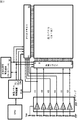
図1には、この発明に係る液晶駆動回路を用いた液晶表示装置の一実施例の概略ブロック図が示されている。同図には、液晶表示パネルとその信号線(セグメント)に供給される表示出力信号を形成する液晶駆動回路及びそのコントロール回路が代表として例示的に示され、液晶表示パネルの表示に必要な走査線駆動回路は本発明に直接関係が無いので省略されている。 FIG. 1 is a schematic block diagram showing an embodiment of a liquid crystal display device using a liquid crystal driving circuit according to the present invention. In the drawing, a liquid crystal display panel, a liquid crystal driving circuit for forming a display output signal supplied to the signal lines (segments) thereof, and a control circuit for the liquid crystal display panel are exemplarily shown as representatives, and scanning necessary for the display of the liquid crystal display panel is shown. The line driving circuit is omitted because it is not directly related to the present invention.
液晶表示パネルLCDの縦方向に延長されるようにされる信号線電極は、高精細化のために高密度に形成される。それ故、半導体集積回路装置により構成される液晶駆動回路の出力端子のピッチと、上記液晶表示パネルLCDの信号線電極のピッチとを合わせ込むために、特に制限されないが、信号線は奇数番目と偶数番目のものを駆動する液晶駆動回路が上下に振り分けられる。 The signal line electrodes extended in the vertical direction of the liquid crystal display panel LCD are formed with high density for high definition. Therefore, in order to match the pitch of the output terminals of the liquid crystal driving circuit constituted by the semiconductor integrated circuit device and the pitch of the signal line electrodes of the liquid crystal display panel LCD, there is no particular limitation. Liquid crystal driving circuits for driving even-numbered ones are distributed up and down.
例えば、下側に設けられた液晶駆動回路SDL1〜SDL5…等は、奇数番目の信号線を駆動するようにされ、上側に設けられた液晶駆動回路SDR1〜SDR5…等は、偶数番目の信号線を駆動するようにされる。このように駆動回路を表示パネルの上下に振り分けることにより、液晶駆動回路からみた液晶表示パネルの信号線のピッチを2倍に広くでき、液晶駆動回路の出力端子とそれに接続される液晶表示パネルLCDの信号線のピッチをほぼ合わせ込むことができる。 For example, the lower liquid crystal drive circuits SDL1 to SDL5... Are driven to drive odd-numbered signal lines, and the upper liquid crystal drive circuits SDR1 to SDR5. To be driven. By allocating the drive circuit above and below the display panel in this way, the pitch of the signal lines of the liquid crystal display panel viewed from the liquid crystal drive circuit can be doubled, and the output terminal of the liquid crystal drive circuit and the liquid crystal display panel LCD connected thereto The pitch of the signal lines can be almost matched.
この実施例の液晶駆動回路SDL1〜SDR5等は、それぞれが入力端子と出力端子を持つようにされる。つまり、入力端子からはシリアルに入力される画像データDATAと交流化信号及びクロックパルスTP等が供給される。これらの信号DATA,TPは、そのまま出力回路と出力端子を通して出力させるようにする。 Each of the liquid crystal driving circuits SDL1 to SDR5 in this embodiment has an input terminal and an output terminal. That is, serially input image data DATA, an alternating signal, a clock pulse TP, and the like are supplied from the input terminal. These signals DATA and TP are output as they are through the output circuit and the output terminal.
液晶表示パネルLCDは、高精細化や大画面等により約600本〜1000本もの信号線を持つのに対して、半導体集積回路装置により構成される液晶駆動回路は、80ないし160本程度の出力端子しか持ち得ない。そのため、1つの液晶表示パネルLCDを駆動するためには多数個の液晶駆動回路が用いられ、1ライン分のシリアル入力される画像データDATAは、各液晶駆動回路が順次に取り込むようにされる。つまり、パネルの左端の初段の液晶駆動回路SDL1(SDR1)が有効となって、それに対応した画像データDATAの取り込みが終了すると、次段の液晶駆動回路SDL2(SDR2)が有効となってそれに対応した画像データDATAを取り込むという動作を繰り返す。 A liquid crystal display panel LCD has about 600 to 1000 signal lines due to high definition, a large screen, etc., whereas a liquid crystal driving circuit constituted by a semiconductor integrated circuit device has about 80 to 160 outputs. Can only have a terminal. Therefore, a large number of liquid crystal drive circuits are used to drive one liquid crystal display panel LCD, and image data DATA input serially for one line is sequentially fetched by each liquid crystal drive circuit. That is, when the first-stage liquid crystal drive circuit SDL1 (SDR1) at the left end of the panel is enabled and the capture of the image data DATA corresponding thereto is completed, the next-stage liquid crystal drive circuit SDL2 (SDR2) is enabled and responds to it. The operation of taking in the image data DATA is repeated.
この実施例では、従来のように実装基板上に形成された入力信号線に対して液晶駆動回路がパラレルに接続されのではなく、各液晶駆動回路を通して順次にクロックパルスTPとそれに同期して入力されるシリアル画像データDATAと、交流化信号が供給される。それ故、下側の液晶駆動回路SDL1〜SDL5を例にして説明すると、初段の液晶駆動回路SDL1にシリアル画像データが取り込まれると、かかる液晶駆動回路SDL1の入力回路及び内部配線と出力回路が信号伝送経路として用いられて次段の液晶駆動回路SDL2に伝えられる。このとき、上記内部配線や出力回路は、遅延回路として利用され、次段の液晶駆動回路SDL2に伝えられる入力信号は、コントロール回路CONTから出力される信号バスの信号DATA,TP等との関係では遅延させられたものとなる。ただし、上記画像データDATAや交流化信号とクロックパルスTPとの相対的な時間関係は保たれているので、その取り込みや表示出力には何ら支障は生じない。以下、上記液晶駆動回路SDL3、SDL4、SDL5…の順に入力信号が伝えられ、その前段回路は遅延回路として作用させられる。 In this embodiment, the liquid crystal driving circuit is not connected in parallel to the input signal lines formed on the mounting substrate as in the prior art, but is sequentially input in synchronization with the clock pulse TP through each liquid crystal driving circuit. Serial image data DATA and an alternating signal are supplied. Therefore, the lower liquid crystal drive circuits SDL1 to SDL5 will be described as an example. When serial image data is taken into the first-stage liquid crystal drive circuit SDL1, the input circuit and internal wiring and output circuit of the liquid crystal drive circuit SDL1 are signaled. It is used as a transmission path and transmitted to the next stage liquid crystal drive circuit SDL2. At this time, the internal wiring and the output circuit are used as a delay circuit, and the input signal transmitted to the liquid crystal drive circuit SDL2 in the next stage is not related to the signals DATA, TP, etc. of the signal bus output from the control circuit CONT. It will be delayed. However, since the relative time relationship between the image data DATA and the AC signal and the clock pulse TP is maintained, there is no problem with the capture and display output. In the following, input signals are transmitted in the order of the liquid crystal driving circuits SDL3, SDL4, SDL5..., And the preceding circuit is made to act as a delay circuit.
このため、シリアルに入力された画像データは、各液晶駆動回路SDL1〜SDL5等での遅延時間に相当する時間だけずれて順次に液晶駆動回路SDL2〜SDL5等に取り込まれるとともに、パラレル出力動作を行う表示タイミングTPも同様に遅延させられるために、上記の遅延時間だけずれて、初段の液晶駆動回路SDL1、第2段目の液晶駆動回路SDL2・・・・・図示しない最終段の液晶駆動回路のように表示出力信号が出力される。このことは、上側の液晶駆動回路SDR1〜SDR5等においても同様である。 For this reason, the serially input image data is sequentially taken into the liquid crystal drive circuits SDL2 to SDL5, etc., shifted by a time corresponding to the delay time in each of the liquid crystal drive circuits SDL1 to SDL5, and performs a parallel output operation. Since the display timing TP is similarly delayed, the first-stage liquid crystal drive circuit SDL1, the second-stage liquid crystal drive circuit SDL2,... Thus, a display output signal is output. The same applies to the upper liquid crystal drive circuits SDR1 to SDR5.
これにより、表示駆動電流が上記のように液晶駆動回路の数ずつが分散されて出力されるために、高精細化や大画面化により信号線の数が増大しても実装基板上の電源線に流れるピーク電流が分散されて流れることになる。これにより、電源線に流れるピーク電流を大幅に低減させることができる。 As a result, the display drive current is distributed and output in units of the number of liquid crystal drive circuits as described above. Therefore, even if the number of signal lines increases due to high definition or large screen, the power supply lines on the mounting board The peak current that flows through is distributed and flows. Thereby, the peak current flowing through the power supply line can be greatly reduced.
図2には、この発明に係る液晶駆動回路を用いた液晶表示装置の他の一実施例の概略ブロック図が示されている。同図には、液晶表示パネルとその信号線に供給される表示出力信号を形成する液晶駆動回路及びそのコントロール回路が代表として例示的に示され、液晶表示パネルの表示に必要な走査線駆動回路は本発明に直接関係が無いので省略されている。また、前記のように液晶表示パネルLCDの上側に設けられる液晶駆動回路も省略されている。 FIG. 2 is a schematic block diagram showing another embodiment of the liquid crystal display device using the liquid crystal driving circuit according to the present invention. In the figure, a liquid crystal display panel, a liquid crystal driving circuit for forming a display output signal supplied to the signal line, and a control circuit for the liquid crystal display panel are exemplarily shown as representatives, and a scanning line driving circuit necessary for the display of the liquid crystal display panel is shown. Are omitted because they are not directly related to the present invention. Further, as described above, the liquid crystal driving circuit provided on the upper side of the liquid crystal display panel LCD is also omitted.
この実施例の液晶駆動回路では、80本ないし160本程度の表示出力信号しか持ち得ないのに対して、駆動される液晶表示パネルLCDの信号線の数は高精細化や大画面化により1000本以上に増大される傾向にあり、上記液晶駆動回路の数も多くなって、最終段回路では加算された遅延時間により1つの走査タイミング期間に表示出力が間に合わなくなってしまう虞れがある。つまり、表示データのシリアル取り込み信号の周期Tの1/2を上限にして最終段の液晶駆動回路に対する遅延時間を設定する必要がある。逆に、従来回路における電源ノイズのピーク部の時間幅が約20ns程度であるので、これと同じかそれより大きくなるように最終段液晶駆動回路の総遅延時間が設定される必要がある。この実施例では、表示出力数と上記のような遅延時間の条件を考慮して液晶駆動回路を複数組に分割して構成される。 The liquid crystal driving circuit of this embodiment can only have about 80 to 160 display output signals, whereas the number of signal lines of the liquid crystal display panel LCD to be driven is 1000 due to high definition and large screen. There is a tendency that the number of liquid crystal driving circuits is increased, and the number of the liquid crystal driving circuits is increased. In the final stage circuit, there is a possibility that the display output may not be in time for one scanning timing period due to the added delay time. In other words, it is necessary to set the delay time for the liquid crystal drive circuit at the final stage with an upper limit of 1/2 of the period T of the serial capture signal of the display data. On the contrary, since the time width of the peak portion of the power supply noise in the conventional circuit is about 20 ns, it is necessary to set the total delay time of the final stage liquid crystal driving circuit so as to be equal to or larger than this. In this embodiment, the liquid crystal driving circuit is divided into a plurality of sets in consideration of the number of display outputs and the delay time conditions as described above.
この実施例では、液晶駆動回路が奇数番目と偶数番目の液晶駆動回路に2分割される。つまり、第1と第3及び第5段目の液晶駆動回路が初段回路としてコントロール回路CONTから出力される画像データDATAやクロックパルスTP等をパラレルに取り込むようにされる。そして、偶数番目の液晶駆動回路SDL2、SDL4等は、その前段とされる液晶駆動回路SDL1、SDL3等を通して入力される遅延信号が供給される。 In this embodiment, the liquid crystal driving circuit is divided into two odd-numbered and even-numbered liquid crystal driving circuits. That is, the first, third, and fifth-stage liquid crystal drive circuits are configured to capture in parallel the image data DATA, the clock pulse TP, and the like output from the control circuit CONT as the first-stage circuit. The even-numbered liquid crystal drive circuits SDL2, SDL4, etc. are supplied with delay signals that are input through the liquid crystal drive circuits SDL1, SDL3, etc., which are the preceding stages.
この構成では、液晶表示パネルLCDの高精細化や大画面化により、いかに液晶駆動回路の数が増大しようとも、表示出力タイミングが2つに分割されるのもであるので、例えば表示データのシリアル取り込み信号の周期Tの1/2を上限にし、電源ノイズのピーク部の時間幅を下限とする範囲を広くでき、各液晶駆動回路での遅延時間の設定が容易になる。 In this configuration, even if the number of liquid crystal drive circuits increases due to the high definition and large screen of the liquid crystal display panel LCD, the display output timing is divided into two. The range in which 1/2 of the period T of the captured signal is set as the upper limit and the time width of the peak portion of the power supply noise is set as the lower limit can be widened, and the delay time can be easily set in each liquid crystal driving circuit.
図3には、この発明に係る液晶駆動回路を用いた液晶表示装置の更に他の一実施例の概略ブロック図が示されている。この実施例では、表示出力タイミングが3つに分割する例が示されている。つまり、入力の信号バスに対して、3個ずつの液晶駆動回路SDL1〜SDL3等が縦列形態にされるようにする。これにより、液晶駆動回路の出力タイミングを3つに分散させて電源線に発生するピーク電流をほぼ1/3に緩和させることができる。以下、同様に縦列形態にされる液晶駆動回路の数を増加すれば、それに応じて電源線に流れるピーク電流値も低減され、最終的には図1の実施例が最もピーク電流が小さくされるが、反面遅延時間の制約による限界が生じるものとなる。 FIG. 3 is a schematic block diagram showing still another embodiment of the liquid crystal display device using the liquid crystal driving circuit according to the present invention. In this embodiment, an example in which the display output timing is divided into three is shown. That is, three liquid crystal driving circuits SDL1 to SDL3 are arranged in a column for the input signal bus. As a result, the output timing of the liquid crystal driving circuit can be dispersed into three, and the peak current generated in the power supply line can be reduced to approximately 1/3. Hereinafter, if the number of liquid crystal drive circuits similarly arranged in a column is increased, the peak current value flowing through the power supply line is also reduced accordingly, and finally the embodiment of FIG. 1 has the smallest peak current. However, there is a limit due to delay time constraints.
図4には、液晶駆動回路の一実施例の概略ブロック図が示されている。この実施例では、入力端子には入力回路としての入力保護回路が設けられる。これらの保護回路を通した信号は、内部配線を通して内部ロジック・駆動回路(ドライバ)等に供給される。内部配線には、バッファ(出力)回路が設けられて出力端子から信号送出を行う機能が設けられる。これらの内部配線での信号伝播遅延時間やバッファ回路での信号伝播遅延時間により、出力端子から出力される信号は、入力端子から入力れる各信号に対して遅延させられるものとなる。 FIG. 4 shows a schematic block diagram of an embodiment of the liquid crystal driving circuit. In this embodiment, the input terminal is provided with an input protection circuit as an input circuit. Signals that pass through these protection circuits are supplied to internal logic / driving circuits (drivers) through internal wiring. The internal wiring is provided with a buffer (output) circuit and a function of sending a signal from the output terminal. Due to the signal propagation delay time in these internal wirings and the signal propagation delay time in the buffer circuit, the signal output from the output terminal is delayed with respect to each signal input from the input terminal.
上記入力保護回路は、入力端子から入り込んでくる急峻電流や静電気による破壊から内部回路を保護するとともに、内部ロジックや駆動回路へ信号伝達する際の入力波形の歪の整形と振幅を安定化させる。すなわち、外部と内部配線を電気的に分離させる役割を持ち、半導体装置一般に設けられることが常識となっている回路である。 The input protection circuit protects the internal circuit from destruction caused by a steep current or static electricity entering from the input terminal, and stabilizes the shaping and amplitude of the distortion of the input waveform when a signal is transmitted to the internal logic or the drive circuit. That is, it is a circuit that has a role of electrically separating external and internal wiring and is commonly provided in semiconductor devices.
入力端子から供給されるタイミング信号は、後述するようなラインクロック信号CL1、データラッチクロック信号CL2、交流化信号Mの3本であり、画像データDATAは、特に制限されないが、4ビットデータとされる。このため、入力端子の合計7本とされる。なお、後述するような駆動電圧発生回路により形成された駆動電圧が入力される入力端子は、一種の電源端子と見做されるので同図では省略されている。 There are three timing signals supplied from the input terminal: a line clock signal CL1, a data latch clock signal CL2, and an alternating signal M, which will be described later. The image data DATA is not particularly limited, but is 4-bit data. The For this reason, a total of seven input terminals are provided. Note that an input terminal to which a drive voltage formed by a drive voltage generation circuit, which will be described later, is input is regarded as a kind of power supply terminal and is omitted in FIG.
内部ロジック・駆動回路は、後述するようにシリアル/パラレル変換動作を行うラインデータラッチ回路と、データラッチ回路の出力信号をレベルシフトを行うレベルシフト回路と、このレベルシフト回路を通した出力信号により駆動されて、駆動電圧を出力させる出力MOSFET(ドライバ)から構成される。 As will be described later, the internal logic / drive circuit includes a line data latch circuit that performs serial / parallel conversion operation, a level shift circuit that shifts the output signal of the data latch circuit, and an output signal that passes through the level shift circuit. The output MOSFET (driver) is driven to output a driving voltage.
図5には、液晶駆動回路の他の一実施例の概略ブロック図が示されている。液晶駆動回路においては、前記図1のように液晶表示パネルの上下に振り分けられて実装基板に設けられることが多い。このため、前記図1の実施例のように入力端子と出力端子とが固定されているときには、表示パネルの上側と下側に配置される液晶駆動回路とでは、一方側では入力端子と出力端子とが順に接続されて実装基板上の配線は最短にされる。これに対して、他方側では、信号伝達方向と入力端子と出力端子とが逆になるため、実装基板上に形成される配線長が長くなるとともに、入力側と出力側とが交差してしまう。 FIG. 5 shows a schematic block diagram of another embodiment of the liquid crystal driving circuit. In the liquid crystal driving circuit, as shown in FIG. 1, the liquid crystal driving circuit is often arranged on the mounting substrate by being divided up and down the liquid crystal display panel. For this reason, when the input terminal and the output terminal are fixed as in the embodiment of FIG. 1, the liquid crystal driving circuit disposed on the upper side and the lower side of the display panel has an input terminal and an output terminal on one side. Are connected in order, and the wiring on the mounting board is minimized. On the other hand, on the other side, since the signal transmission direction, the input terminal, and the output terminal are reversed, the length of the wiring formed on the mounting board becomes long, and the input side and the output side cross each other. .
この実施例では、入力端子と出力端子とを入れ換えて使用できるように、2組の入出力端子に対応してそれぞれ双方向バッファが設けられる。双方向バッファは、入力保護回路を通してシフト方向制御信号が供給されて、その信号伝達方向が決定される。例えば、シフト方向制御信号がハイレベルなら、入出力端子Lが入力端子とされ、それに対応して設けられた双方向バッファが入力回路として動作させられる。このとき、入力回路として動作させられる双方向バッファは、前記入力保護回路の機能も兼ねるようにされる。上記のシフト方向制御信号がハイレベルのときには入出力端子Rに対応して設けられた双方向バッファが出力回路として動作させられる。それ故、かかる入出力端子Rは出力端子として用いられる。このような構成により、例えば図1の下側に設けられた液晶駆動回路として動作させられる。 In this embodiment, a bidirectional buffer is provided for each of the two sets of input / output terminals so that the input terminal and the output terminal can be used interchangeably. The bidirectional buffer is supplied with a shift direction control signal through an input protection circuit, and its signal transmission direction is determined. For example, if the shift direction control signal is at a high level, the input / output terminal L is used as an input terminal, and a bidirectional buffer provided corresponding thereto is operated as an input circuit. At this time, the bidirectional buffer operated as the input circuit also serves as the function of the input protection circuit. When the shift direction control signal is at a high level, a bidirectional buffer provided corresponding to the input / output terminal R is operated as an output circuit. Therefore, the input / output terminal R is used as an output terminal. With such a configuration, for example, the liquid crystal driving circuit provided on the lower side of FIG. 1 is operated.
逆に、シフト方向制御信号がロウレベルなら、入出力端子Rが入力端子とされ、それに対応して設けられた双方向バッファが入力回路として動作させられる。このとき、入力回路として動作させられる双方向バッファは、上記同様に入力保護回路の機能も兼ねるようにされる。上記のシフト方向制御信号がロウレベルのときには入出力端子Lに対応して設けられた双方向バッファが出力回路として動作させられる。それ故、かかる入出力端子Lは出力端子として用いられる。このような構成により、例えば図1の上側に設けられた液晶駆動回路として動作させられる。 Conversely, if the shift direction control signal is at a low level, the input / output terminal R is used as an input terminal, and a bidirectional buffer provided corresponding thereto is operated as an input circuit. At this time, the bidirectional buffer operated as the input circuit also functions as an input protection circuit as described above. When the shift direction control signal is at a low level, a bidirectional buffer provided corresponding to the input / output terminal L is operated as an output circuit. Therefore, the input / output terminal L is used as an output terminal. With such a configuration, for example, the liquid crystal drive circuit provided on the upper side of FIG. 1 is operated.
このような構成により、実装基板上では最短距離をもって液晶駆動回路を縦列形態に接続させることができる。そして、半導体集積回路装置に形成された内部配線が信号伝達経路として利用されるものであるために、実装基板上に形成されるプリント領域を減らすことができ、配線レイアウトの簡素化を図ることができるものとなる。 With such a configuration, the liquid crystal driving circuits can be connected in a column form with the shortest distance on the mounting substrate. Since the internal wiring formed in the semiconductor integrated circuit device is used as a signal transmission path, the print area formed on the mounting substrate can be reduced, and the wiring layout can be simplified. It will be possible.
図6には、この発明に係る液晶駆動回路を液晶表示モジュールに実装したときの一実施例の要部外観図が示されている。この実施例では、特に制限されないが、テープキャリア方式によってなる液晶駆動装置が液晶表示パネルとプリント基板に実装される。画素データとタイミングパルスに対応する入力側アウタリード端子がプリント基板の配線層により電気的に結線される状態が示されている。このようにして、複数個から半導体チップに形成された液晶駆動回路の入力端子と出力端子とが順に接続される。 FIG. 6 shows an external view of the main part of one embodiment when the liquid crystal driving circuit according to the present invention is mounted on a liquid crystal display module. In this embodiment, although not particularly limited, a liquid crystal driving device based on a tape carrier system is mounted on a liquid crystal display panel and a printed board. The state where the input side outer lead terminal corresponding to the pixel data and the timing pulse is electrically connected by the wiring layer of the printed board is shown. In this way, a plurality of input terminals and output terminals of the liquid crystal driving circuit formed on the semiconductor chip are sequentially connected.
図7には、この発明に係る液晶表示装置の一実施例の概略全体ブロック図が示されている。液晶表示パネル制御装置は、マイクロプロセッサCPU等から表示データを受けて、表示パネルの動作に必要なクロックパルスCL1,CL2、表示データDin、フレーム信号FLMを形成する。 FIG. 7 is a schematic overall block diagram of an embodiment of the liquid crystal display device according to the present invention. The liquid crystal display panel control device receives display data from a microprocessor CPU or the like, and generates clock pulses CL1 and CL2, display data Din, and a frame signal FLM necessary for the operation of the display panel.
この実施例では、1フレーム(1画面の表示期間)毎に交流化のための極性を切り換えると、比較的低い周波数により極性反転が行われて交流化に伴う画面のチラツキが問題になる。そこで、1フレーム中の複数走査線毎に極性を切り換えて、交流化周波数を数百Hzのように高くして交流化に伴うチラツキを防止する。このため、交流化信号発生回路が設けられ、走査線に選択タイミングに対応したクロックパルスCL1を計数して、複数走査線毎に交流化信号Mの極性を変化させる。 In this embodiment, when the polarity for alternating current is switched every frame (display period of one screen), polarity inversion is performed at a relatively low frequency, causing screen flickering due to alternating current. Therefore, the polarity is switched for each of a plurality of scanning lines in one frame, and the alternating frequency is increased to several hundred Hz to prevent flickering due to alternating current. For this reason, an AC signal generation circuit is provided, and the clock pulse CL1 corresponding to the selection timing is counted on the scanning line, and the polarity of the AC signal M is changed for each of the scanning lines.
直列抵抗とオペアンプは、電圧発生回路であり、駆動電圧V1〜V6を形成して、走査ドライバ及びデータドライバに供給する。液晶表示パネルは、走査線の数がX1ないしXmのm本からなり、信号線がY1ないしYnのn本から構成される。これにより、液晶表示パネルは、m×nのような画素から構成される。 The series resistor and the operational amplifier are voltage generation circuits that form drive voltages V1 to V6 and supply them to the scan driver and the data driver. The liquid crystal display panel is composed of m scanning lines X1 to Xm and n signal lines Y1 to Yn. As a result, the liquid crystal display panel is composed of pixels such as m × n.
走査線駆動回路は、複数の半導体集積回路装置から構成され、クロックパルスCL1により、シフト動作を行うシフトレジスタと、その出力信号を受けて駆動電圧発生回路により形成された駆動電圧V1又はV5とV2又はV6を交流化信号により切り替えて対応する走査線電極に出力させて走査線電極を選択/非選択レベルにする。 The scanning line driving circuit is composed of a plurality of semiconductor integrated circuit devices, and a driving voltage V1 or V5 and V2 formed by a driving voltage generating circuit in response to a shift register that performs a shifting operation by a clock pulse CL1 and an output signal thereof. Alternatively, V6 is switched by an AC signal and output to the corresponding scanning line electrode to set the scanning line electrode to the selection / non-selection level.
シフトレジスタの出力信号が選択レベルにされると、駆動電圧V1を対応した走査線電極に出力する。このとき、他の走査線駆動電圧は、シフトレジスタの出力信号の非選択レベルに応じて駆動電圧V5にされる。シフトレジスタは、クロックパルスCL1に同期し、上記選択レベルを順次シフトするので、次のタイミングでは、次の走査線電極が代わって選択レベルにされる。このようにして、走査線電極が順次選択される。上記のように、1フレーム中の複数走査線毎に極性を切り換えるものでは、交流化信号Mにより、駆動電圧V1に代えてV2のような選択レベルに、V5に代えてV6のような非選択レベルにされる。 When the output signal of the shift register is set to the selection level, the drive voltage V1 is output to the corresponding scanning line electrode. At this time, the other scanning line driving voltage is set to the driving voltage V5 according to the non-selection level of the output signal of the shift register. Since the shift register sequentially shifts the selection level in synchronization with the clock pulse CL1, at the next timing, the next scanning line electrode is set to the selection level instead. In this way, the scanning line electrodes are sequentially selected. As described above, in the case of switching the polarity for each of a plurality of scanning lines in one frame, the AC signal M causes a selection level such as V2 instead of the driving voltage V1 and non-selection such as V6 instead of V5. To the level.
画素データDinは、クロックパルスCL2に同期してシリアル/パラレル変換回路にシリアルに入力される。1走査線分に対応した信号線電極の画素信号は、1H期間(クロックパルスCL1の1周期内)に、クロックパルスCL2に同期してシリアルに入力される。このようにシリアルに取り込まれた1走査線分の画素信号は、パラレルに前記のようなラインデータラッチ回路に取り込まれる。 The pixel data Din is serially input to the serial / parallel conversion circuit in synchronization with the clock pulse CL2. The pixel signal of the signal line electrode corresponding to one scanning line is serially input in synchronization with the clock pulse CL2 in the 1H period (within one cycle of the clock pulse CL1). Thus, the pixel signals for one scanning line captured serially are captured in parallel by the line data latch circuit as described above.
信号線駆動回路は、上記のように複数個からなる液晶駆動回路により構成されるものであり、上記のようなシリアル/パラレル変換動作を行うラインデータラッチ回路と、レベルシフト回路に供給してレベルシフトを行う。すなわち、ラインデータラッチ回路は、5V系の回路により構成されており、5Vのようなハイレベルと、0Vのようなロウレベルを出力する。これに対して、ドライバはスイッチMOSFETから構成されており、駆動電圧発生回路により形成された駆動電圧V1、V3,V4及びV2のような比較的大きな電圧範囲の電圧をレベル損失なく出力させるように上記ラッチ回路の出力信号をレベルシフト回路によりレベルシフトさせるものである。 The signal line drive circuit is composed of a plurality of liquid crystal drive circuits as described above, and is supplied to the line data latch circuit that performs the serial / parallel conversion operation as described above and the level shift circuit to provide the level. Shift. That is, the line data latch circuit is composed of a 5V system circuit, and outputs a high level such as 5V and a low level such as 0V. On the other hand, the driver is composed of a switch MOSFET, and outputs a voltage in a relatively large voltage range such as driving voltages V1, V3, V4 and V2 formed by the driving voltage generation circuit without level loss. The output signal of the latch circuit is level-shifted by a level shift circuit.
上記の実施例から得られる作用効果は、下記の通りである。すなわち、
(1) クロックパルスに同期してシリアルに入力された画像データを取り込み、表示タイミング信号に従ってシリアルに取り込まれた画像データに基づいて形成された表示出力信号をパラレルに出力させる液晶駆動回路に入力端子の他に出力回路と出力端子を設けておき、複数からなる液晶駆動回路を縦列形態に接続し、液晶駆動回路における内部配線及び出力回路を遅延手段として用いて各液晶駆動回路毎の表示出力信号の出力タイミングが時間的に分散されるようにすることにより、高精細化や大画面化においても、実装基板上の電源線に流れるピーク電流値を低減されるので電源ノイズによる表示品質の低下や誤動作を防止できるという効果が得られる。
(2) 上記入力回路と出力回路は、制御信号に従って双方向に信号伝達方向が切り替えられる双方向バッファとし、それに対応して入力端子と出力端子が決めるようにすることにより、表示パネルの信号電極の両側に液晶駆動回路を振り分けて設けるときに、実装基板上において上記液晶駆動回路を縦列形態に接続させる配線を最短に形成できるという効果が得られる。
(3) シリアルな画像データに対応して液晶駆動回路を複数組に分割し、各組における初段回路の入力端子には、実装基板上に形成された入力信号線に対してパラレルに接続し、各組の初段回路の出力回路の信号が次段回路の入力信号とされるように縦列接続させることにより、液晶表示パネルの高精細化や大画面に対して、表示データのシリアル取り込み信号の周期に対応した上限の遅延時間と電源ノイズのピーク部の時間幅を考慮して下限との範囲を広くできるという効果が得られる。
The effects obtained from the above embodiment are as follows. That is,
(1) An input terminal for a liquid crystal driving circuit that captures image data input serially in synchronization with a clock pulse and outputs a display output signal formed based on the image data serially captured in accordance with a display timing signal in parallel In addition to this, an output circuit and an output terminal are provided, a plurality of liquid crystal drive circuits are connected in a tandem form, and display output signals for each liquid crystal drive circuit using the internal wiring and output circuit in the liquid crystal drive circuit as delay means By distributing the output timing in terms of time, the peak current value flowing through the power supply line on the mounting board can be reduced even in high definition and large screens. An effect of preventing malfunction can be obtained.
(2) The input circuit and the output circuit are bidirectional buffers in which the signal transmission direction can be switched bidirectionally in accordance with the control signal, and the input terminal and the output terminal are determined in accordance with the bidirectional buffer. When the liquid crystal driving circuits are distributed and provided on both sides, an effect is obtained that the wiring for connecting the liquid crystal driving circuits in a column form on the mounting substrate can be formed in the shortest time.
(3) The liquid crystal drive circuit is divided into a plurality of sets corresponding to serial image data, and the input terminals of the first stage circuit in each set are connected in parallel to the input signal lines formed on the mounting board, By connecting the output circuit signal of the first stage circuit of each group in cascade so that it becomes the input signal of the next stage circuit, the period of the serial capture signal of the display data for high definition and large screen of the liquid crystal display panel In consideration of the upper limit delay time corresponding to the above and the time width of the peak portion of the power supply noise, the range of the lower limit can be widened.
以上本発明者よりなされた発明を実施例に基づき具体的に説明したが、本願発明は前記実施例に限定されるものではなく、その要旨を逸脱しない範囲で種々変更可能であることはいうまでもない。例えば、表示パネルは、必ずしも高精細化あるいは大画面化されたものでなくともよい。このように信号線の数が少ない場合には、電源装置の電源供給能力の小さな安価なものを用いたり、実装基板に形成される配線を細くしたものを用いることができる等の利点が生じる。 The invention made by the inventor has been specifically described based on the embodiments. However, the invention of the present application is not limited to the embodiments, and various modifications can be made without departing from the scope of the invention. Nor. For example, the display panel does not necessarily have to have a high definition or a large screen. When the number of signal lines is small as described above, there are advantages that an inexpensive device with a small power supply capability of the power supply device can be used, or that a thin wiring formed on the mounting substrate can be used.
液晶表示パネルは、上記のような単純マトリックス構成のもの他、TFT(薄膜トランジスタ)を用いた、アクティブマトリッスク構成のものであってもよい。すなわち、この発明は、シリアルに画像データを取り込んで、パラレルに表示信号を出力させる液晶駆動回路と液晶表示装置に広く利用できる。 The liquid crystal display panel may have an active matrix configuration using TFTs (thin film transistors) in addition to the simple matrix configuration described above. In other words, the present invention can be widely used in a liquid crystal driving circuit and a liquid crystal display device that take in image data serially and output a display signal in parallel.
本願において開示される発明のうち代表的なものによって得られる効果を簡単に説明すれば、下記の通りである。すなわち、クロックパルスに同期してシリアルに入力された画像データを取り込み、表示タイミング信号に従ってシリアルに取り込まれた画像データに基づいて形成された表示出力信号をパラレルに出力させる液晶駆動回路に入力端子の他に出力回路と出力端子を設けておき、複数からなる液晶駆動回路を縦列形態に接続し、液晶駆動回路における内部配線及び出力回路を遅延手段として用いて各液晶駆動回路毎の表示出力信号の出力タイミングが時間的に分散されるようにすることにより、高精細化や大画面化においても、実装基板上の電源線に流れるピーク電流値を低減されるので電源ノイズによる表示品質の低下や誤動作を防止できる。 The effects obtained by the representative ones of the inventions disclosed in the present application will be briefly described as follows. That is, the image data input serially in synchronism with the clock pulse is captured, and the liquid crystal drive circuit that outputs in parallel the display output signal formed based on the image data serially captured in accordance with the display timing signal. In addition, an output circuit and an output terminal are provided, and a plurality of liquid crystal drive circuits are connected in a tandem configuration, and the internal wiring and output circuit in the liquid crystal drive circuit are used as delay means for the display output signal for each liquid crystal drive circuit. By distributing the output timing in time, the peak current value flowing through the power supply line on the mounting board can be reduced even in higher definition and larger screens. Can be prevented.
上記入力回路と出力回路は、制御信号に従って双方向に信号伝達方向が切り替えられる双方向バッファとし、それに対応して入力端子と出力端子が決めるようにすることにより、表示パネルの信号電極の両側に液晶駆動回路を振り分けて設けるときに、実装基板上において上記液晶駆動回路を縦列形態に接続させる配線を最短に形成できる。 The input circuit and the output circuit are bi-directional buffers whose signal transmission directions can be switched in both directions according to the control signal, and the input terminal and the output terminal are determined in accordance with the bidirectional buffer. When the liquid crystal driving circuits are distributed and provided, the wiring for connecting the liquid crystal driving circuits in a columnar form on the mounting substrate can be formed in the shortest time.
シリアルな画像データに対応して液晶駆動回路を複数組に分割し、各組における初段回路の入力端子には、実装基板上に形成された入力信号線に対してパラレルに接続し、各組の初段回路の出力回路の信号が次段回路の入力信号とされるように縦列接続させることにより、液晶表示パネルの高精細化や大画面に対して、表示データのシリアル取り込み信号の周期に対応した上限の遅延時間と電源ノイズのピーク部の時間幅を考慮して下限との範囲を広くできる。 The liquid crystal drive circuit is divided into a plurality of sets corresponding to serial image data, and the input terminals of the first stage circuit in each set are connected in parallel to the input signal lines formed on the mounting board. By connecting the output circuit signal of the first-stage circuit in cascade so that it becomes the input signal of the next-stage circuit, it corresponds to the cycle of the serial capture signal of the display data for high definition and large screen of the liquid crystal display panel The range between the upper limit delay time and the lower limit can be widened in consideration of the time width of the peak portion of the power supply noise.
SDL1〜SDL5,SDR1〜SDR5…液晶駆動回路、CONT…コントロール回路、CPU…マイクロプロセッサ。 SDL1 to SDL5, SDR1 to SDR5 ... Liquid crystal drive circuit, CONT ... Control circuit, CPU ... Microprocessor.
Claims (3)
複数本の信号線が接続された半導体集積回路が複数個前記表示領域の周辺に配置されており、
前記半導体集積回路は、画像データに基づいて表示出力信号を形成して前記表示領域に出力させるものであり、
前記画像データは、隣接する半導体集積回路を介して順にそれぞれの半導体集積回路に供給され、
前記表示領域に前記表示出力信号を出力させる表示タイミング信号は、隣接する半導体集積回路を介して順にそれぞれの半導体集積回路に供給され、
前記半導体集積回路はバッファ回路を有しており、該バッファ回路は、前記画像データ及び表示タイミング信号の伝送経路に配置されていることを特徴とする液晶表示装置。 In a liquid crystal display device having a display area in which signal lines and scanning lines are arranged in a matrix,
A plurality of semiconductor integrated circuits to which a plurality of signal lines are connected are arranged around the display area,
The semiconductor integrated circuit forms a display output signal based on image data and outputs it to the display area,
The image data is sequentially supplied to each semiconductor integrated circuit through adjacent semiconductor integrated circuits,
The display timing signal for outputting the display output signal to the display area is sequentially supplied to each semiconductor integrated circuit through adjacent semiconductor integrated circuits,
The semiconductor integrated circuit has a buffer circuit, the buffer circuit, a liquid crystal display apparatus characterized by being arranged in the transmission path of the image data and the display timing signals.
Priority Applications (1)
| Application Number | Priority Date | Filing Date | Title |
|---|---|---|---|
| JP2003371194A JP4005014B2 (en) | 2003-10-30 | 2003-10-30 | Liquid crystal display |
Applications Claiming Priority (1)
| Application Number | Priority Date | Filing Date | Title |
|---|---|---|---|
| JP2003371194A JP4005014B2 (en) | 2003-10-30 | 2003-10-30 | Liquid crystal display |
Related Parent Applications (1)
| Application Number | Title | Priority Date | Filing Date |
|---|---|---|---|
| JP17482294A Division JP3516722B2 (en) | 1994-07-04 | 1994-07-04 | Liquid crystal drive circuit and liquid crystal display |
Related Child Applications (1)
| Application Number | Title | Priority Date | Filing Date |
|---|---|---|---|
| JP2004244851A Division JP2005018089A (en) | 2004-08-25 | 2004-08-25 | Display device |
Publications (2)
| Publication Number | Publication Date |
|---|---|
| JP2004110063A JP2004110063A (en) | 2004-04-08 |
| JP4005014B2 true JP4005014B2 (en) | 2007-11-07 |
Family
ID=32290955
Family Applications (1)
| Application Number | Title | Priority Date | Filing Date |
|---|---|---|---|
| JP2003371194A Expired - Lifetime JP4005014B2 (en) | 2003-10-30 | 2003-10-30 | Liquid crystal display |
Country Status (1)
| Country | Link |
|---|---|
| JP (1) | JP4005014B2 (en) |
Families Citing this family (2)
| Publication number | Priority date | Publication date | Assignee | Title |
|---|---|---|---|---|
| KR101197057B1 (en) * | 2005-12-12 | 2012-11-06 | 삼성디스플레이 주식회사 | Display device |
| KR102263319B1 (en) | 2015-01-30 | 2021-06-09 | 삼성전자주식회사 | Display Controller for improving display noise and System including the same |
-
2003
- 2003-10-30 JP JP2003371194A patent/JP4005014B2/en not_active Expired - Lifetime
Also Published As
| Publication number | Publication date |
|---|---|
| JP2004110063A (en) | 2004-04-08 |
Similar Documents
| Publication | Publication Date | Title |
|---|---|---|
| US7683873B2 (en) | Liquid crystal display driver device and liquid crystal display system | |
| US7936328B2 (en) | Display panel including amplifier with offset canceling by reversing polarity of amplifier offset | |
| KR101410955B1 (en) | Display apparatus and method of driving the display apparatus | |
| US8159431B2 (en) | Electrooptic device and electronic apparatus | |
| US20150138176A1 (en) | Scanning signal line drive circuit and display device provided with same | |
| US7592992B2 (en) | Inversion method for liquid crystal display | |
| US8310430B2 (en) | Display device and display driver with output switching control | |
| JP2004301946A (en) | Driving device and display module equipped with the same | |
| US9886928B2 (en) | Gate signal line drive circuit | |
| US8587509B2 (en) | Display device and drive method for driving the same | |
| US8786542B2 (en) | Display device including first and second scanning signal line groups | |
| KR20030065286A (en) | Display panel drive circuit and plasma display | |
| JP2008015464A (en) | Liquid crystal display device and method of driving the same | |
| JPH0822267A (en) | Liquid crystal driving circuit and liquid crystal display device | |
| JP2011128219A (en) | Display device and method for driving display device | |
| JP3516722B2 (en) | Liquid crystal drive circuit and liquid crystal display | |
| KR100862945B1 (en) | A liquid crystal display device of chip on glass type | |
| JP2009181612A (en) | Shift register circuit and liquid crystal display unit | |
| JP4170334B2 (en) | Liquid crystal display | |
| JP4005014B2 (en) | Liquid crystal display | |
| JP2011112971A (en) | Display device and method of driving the same | |
| CN113299215B (en) | Gate driving circuit | |
| JP2000276110A (en) | Liquid crystal display device | |
| JP2005018089A (en) | Display device | |
| KR101174630B1 (en) | Display panel and display apparatus |
Legal Events
| Date | Code | Title | Description |
|---|---|---|---|
| A621 | Written request for application examination |
Free format text: JAPANESE INTERMEDIATE CODE: A621 Effective date: 20031104 |
|
| A131 | Notification of reasons for refusal |
Free format text: JAPANESE INTERMEDIATE CODE: A131 Effective date: 20040629 |
|
| A521 | Written amendment |
Free format text: JAPANESE INTERMEDIATE CODE: A523 Effective date: 20040825 |
|
| A521 | Written amendment |
Free format text: JAPANESE INTERMEDIATE CODE: A523 Effective date: 20040825 |
|
| A131 | Notification of reasons for refusal |
Free format text: JAPANESE INTERMEDIATE CODE: A131 Effective date: 20041116 |
|
| A521 | Written amendment |
Free format text: JAPANESE INTERMEDIATE CODE: A523 Effective date: 20050114 |
|
| A02 | Decision of refusal |
Free format text: JAPANESE INTERMEDIATE CODE: A02 Effective date: 20050315 |
|
| A521 | Written amendment |
Free format text: JAPANESE INTERMEDIATE CODE: A523 Effective date: 20050512 |
|
| A521 | Written amendment |
Free format text: JAPANESE INTERMEDIATE CODE: A523 Effective date: 20050712 |
|
| A911 | Transfer of reconsideration by examiner before appeal (zenchi) |
Free format text: JAPANESE INTERMEDIATE CODE: A911 Effective date: 20050720 |
|
| A912 | Removal of reconsideration by examiner before appeal (zenchi) |
Free format text: JAPANESE INTERMEDIATE CODE: A912 Effective date: 20050902 |
|
| A521 | Written amendment |
Free format text: JAPANESE INTERMEDIATE CODE: A523 Effective date: 20070725 |
|
| A61 | First payment of annual fees (during grant procedure) |
Free format text: JAPANESE INTERMEDIATE CODE: A61 Effective date: 20070822 |
|
| R150 | Certificate of patent or registration of utility model |
Free format text: JAPANESE INTERMEDIATE CODE: R150 |
|
| FPAY | Renewal fee payment (event date is renewal date of database) |
Free format text: PAYMENT UNTIL: 20100831 Year of fee payment: 3 |
|
| FPAY | Renewal fee payment (event date is renewal date of database) |
Free format text: PAYMENT UNTIL: 20100831 Year of fee payment: 3 |
|
| FPAY | Renewal fee payment (event date is renewal date of database) |
Free format text: PAYMENT UNTIL: 20110831 Year of fee payment: 4 |
|
| S111 | Request for change of ownership or part of ownership |
Free format text: JAPANESE INTERMEDIATE CODE: R313115 Free format text: JAPANESE INTERMEDIATE CODE: R313121 |
|
| FPAY | Renewal fee payment (event date is renewal date of database) |
Free format text: PAYMENT UNTIL: 20110831 Year of fee payment: 4 |
|
| R350 | Written notification of registration of transfer |
Free format text: JAPANESE INTERMEDIATE CODE: R350 |
|
| FPAY | Renewal fee payment (event date is renewal date of database) |
Free format text: PAYMENT UNTIL: 20110831 Year of fee payment: 4 |
|
| FPAY | Renewal fee payment (event date is renewal date of database) |
Free format text: PAYMENT UNTIL: 20120831 Year of fee payment: 5 |
|
| FPAY | Renewal fee payment (event date is renewal date of database) |
Free format text: PAYMENT UNTIL: 20120831 Year of fee payment: 5 |
|
| FPAY | Renewal fee payment (event date is renewal date of database) |
Free format text: PAYMENT UNTIL: 20130831 Year of fee payment: 6 |
|
| R250 | Receipt of annual fees |
Free format text: JAPANESE INTERMEDIATE CODE: R250 |
|
| EXPY | Cancellation because of completion of term |