JP4004484B2 - Manufacturing method of solid-state imaging device - Google Patents
Manufacturing method of solid-state imaging device Download PDFInfo
- Publication number
- JP4004484B2 JP4004484B2 JP2004107904A JP2004107904A JP4004484B2 JP 4004484 B2 JP4004484 B2 JP 4004484B2 JP 2004107904 A JP2004107904 A JP 2004107904A JP 2004107904 A JP2004107904 A JP 2004107904A JP 4004484 B2 JP4004484 B2 JP 4004484B2
- Authority
- JP
- Japan
- Prior art keywords
- region
- conductivity type
- type
- insulating film
- gate electrode
- Prior art date
- Legal status (The legal status is an assumption and is not a legal conclusion. Google has not performed a legal analysis and makes no representation as to the accuracy of the status listed.)
- Expired - Fee Related
Links
- 238000004519 manufacturing process Methods 0.000 title claims description 25
- 238000003384 imaging method Methods 0.000 title claims description 22
- 239000000758 substrate Substances 0.000 claims description 71
- 239000012535 impurity Substances 0.000 claims description 66
- 239000010410 layer Substances 0.000 claims description 51
- 238000009792 diffusion process Methods 0.000 claims description 23
- 238000002955 isolation Methods 0.000 claims description 19
- 238000005468 ion implantation Methods 0.000 claims description 17
- 230000001681 protective effect Effects 0.000 claims description 10
- 238000003860 storage Methods 0.000 claims description 9
- 239000000969 carrier Substances 0.000 claims description 7
- 239000004065 semiconductor Substances 0.000 claims description 7
- 238000000034 method Methods 0.000 claims description 5
- 230000003647 oxidation Effects 0.000 claims description 4
- 238000007254 oxidation reaction Methods 0.000 claims description 4
- 239000002344 surface layer Substances 0.000 claims description 2
- XUIMIQQOPSSXEZ-UHFFFAOYSA-N Silicon Chemical compound [Si] XUIMIQQOPSSXEZ-UHFFFAOYSA-N 0.000 description 45
- 229910052710 silicon Inorganic materials 0.000 description 45
- 239000010703 silicon Substances 0.000 description 45
- 230000003287 optical effect Effects 0.000 description 12
- 230000007547 defect Effects 0.000 description 10
- 238000002513 implantation Methods 0.000 description 10
- 230000015572 biosynthetic process Effects 0.000 description 8
- 239000011229 interlayer Substances 0.000 description 7
- 102000004129 N-Type Calcium Channels Human genes 0.000 description 6
- 108090000699 N-Type Calcium Channels Proteins 0.000 description 6
- 150000002500 ions Chemical class 0.000 description 5
- 238000009825 accumulation Methods 0.000 description 4
- 238000006243 chemical reaction Methods 0.000 description 4
- 238000009826 distribution Methods 0.000 description 4
- 230000035945 sensitivity Effects 0.000 description 4
- 238000000926 separation method Methods 0.000 description 3
- 238000001312 dry etching Methods 0.000 description 2
- 238000002347 injection Methods 0.000 description 2
- 239000007924 injection Substances 0.000 description 2
- 238000001039 wet etching Methods 0.000 description 2
- 108091006146 Channels Proteins 0.000 description 1
- 229910004298 SiO 2 Inorganic materials 0.000 description 1
- VYPSYNLAJGMNEJ-UHFFFAOYSA-N Silicium dioxide Chemical compound O=[Si]=O VYPSYNLAJGMNEJ-UHFFFAOYSA-N 0.000 description 1
- 230000002238 attenuated effect Effects 0.000 description 1
- 238000001514 detection method Methods 0.000 description 1
- 230000000694 effects Effects 0.000 description 1
- 238000009413 insulation Methods 0.000 description 1
- 239000011159 matrix material Substances 0.000 description 1
- 239000012528 membrane Substances 0.000 description 1
- 230000002093 peripheral effect Effects 0.000 description 1
- 229910052814 silicon oxide Inorganic materials 0.000 description 1
Images


Classifications
-
- H—ELECTRICITY
- H01—ELECTRIC ELEMENTS
- H01L—SEMICONDUCTOR DEVICES NOT COVERED BY CLASS H10
- H01L27/00—Devices consisting of a plurality of semiconductor or other solid-state components formed in or on a common substrate
- H01L27/14—Devices consisting of a plurality of semiconductor or other solid-state components formed in or on a common substrate including semiconductor components sensitive to infrared radiation, light, electromagnetic radiation of shorter wavelength or corpuscular radiation and specially adapted either for the conversion of the energy of such radiation into electrical energy or for the control of electrical energy by such radiation
- H01L27/144—Devices controlled by radiation
- H01L27/146—Imager structures
- H01L27/14683—Processes or apparatus peculiar to the manufacture or treatment of these devices or parts thereof
- H01L27/14689—MOS based technologies
-
- B—PERFORMING OPERATIONS; TRANSPORTING
- B01—PHYSICAL OR CHEMICAL PROCESSES OR APPARATUS IN GENERAL
- B01D—SEPARATION
- B01D35/00—Filtering devices having features not specifically covered by groups B01D24/00 - B01D33/00, or for applications not specifically covered by groups B01D24/00 - B01D33/00; Auxiliary devices for filtration; Filter housing constructions
- B01D35/30—Filter housing constructions
- B01D35/306—Filter mounting adapter
-
- B—PERFORMING OPERATIONS; TRANSPORTING
- B01—PHYSICAL OR CHEMICAL PROCESSES OR APPARATUS IN GENERAL
- B01D—SEPARATION
- B01D35/00—Filtering devices having features not specifically covered by groups B01D24/00 - B01D33/00, or for applications not specifically covered by groups B01D24/00 - B01D33/00; Auxiliary devices for filtration; Filter housing constructions
- B01D35/14—Safety devices specially adapted for filtration; Devices for indicating clogging
- B01D35/147—Bypass or safety valves
-
- H—ELECTRICITY
- H01—ELECTRIC ELEMENTS
- H01L—SEMICONDUCTOR DEVICES NOT COVERED BY CLASS H10
- H01L27/00—Devices consisting of a plurality of semiconductor or other solid-state components formed in or on a common substrate
- H01L27/14—Devices consisting of a plurality of semiconductor or other solid-state components formed in or on a common substrate including semiconductor components sensitive to infrared radiation, light, electromagnetic radiation of shorter wavelength or corpuscular radiation and specially adapted either for the conversion of the energy of such radiation into electrical energy or for the control of electrical energy by such radiation
- H01L27/144—Devices controlled by radiation
- H01L27/146—Imager structures
- H01L27/14601—Structural or functional details thereof
- H01L27/14609—Pixel-elements with integrated switching, control, storage or amplification elements
-
- B—PERFORMING OPERATIONS; TRANSPORTING
- B01—PHYSICAL OR CHEMICAL PROCESSES OR APPARATUS IN GENERAL
- B01D—SEPARATION
- B01D2201/00—Details relating to filtering apparatus
- B01D2201/16—Valves
-
- B—PERFORMING OPERATIONS; TRANSPORTING
- B01—PHYSICAL OR CHEMICAL PROCESSES OR APPARATUS IN GENERAL
- B01D—SEPARATION
- B01D2201/00—Details relating to filtering apparatus
- B01D2201/29—Filter cartridge constructions
-
- B—PERFORMING OPERATIONS; TRANSPORTING
- B01—PHYSICAL OR CHEMICAL PROCESSES OR APPARATUS IN GENERAL
- B01D—SEPARATION
- B01D2201/00—Details relating to filtering apparatus
- B01D2201/34—Seals or gaskets for filtering elements
- B01D2201/347—Radial sealings
Description
本発明は、ビデオカメラ、デジタルカメラ、カメラ付き携帯電話器などに用いられる固体撮像素子の製造方法に関し、さらに詳述すれば、閾値電圧変調方式のMOS型イメージセンサなどの固体撮像素子の製造方法に関する。
The present invention is a video camera, a digital camera, relates to a manufacturing method of the solid-state image pickup element used in a camera-equipped mobile telephone and, more specifically, the solid-state imaging element such as a MOS image sensor of a threshold voltage modulation type It relates to a manufacturing method.
従来、画像光を画像信号として電気信号に変換する固体撮像素子として、例えばCCD型イメージセンサ、MOS型イメージセンサなどが知られている。このうち、MOS型イメージセンサは、光照射により電荷を発生する受光領域(フォトダイオード)と、この受光領域で発生した電荷を電気信号として読み出すトランジスタ(MOSトランジスタ)とが共通基板上に設けられている。このようなMOS型イメージセンサは、CCD型イメージセンサに比べて消費電力が少なく、システムLSIなどの標準CMOSプロセス技術を利用することができるために、低コスト化が可能であり、汎用性があるという利点を有している。 Conventionally, as a solid-state imaging device that converts image light into an electrical signal as an image signal, for example, a CCD image sensor, a MOS image sensor, and the like are known. Among these, the MOS type image sensor has a light receiving region (photodiode) that generates charges by light irradiation and a transistor (MOS transistor) that reads the charges generated in the light receiving region as an electric signal on a common substrate. Yes. Such a MOS type image sensor consumes less power than a CCD type image sensor and can use a standard CMOS process technology such as a system LSI. Therefore, the cost can be reduced and versatility is achieved. Has the advantage.
一方、近年では、イオン注入装置の発達に伴って、例えば特許文献1(特開2002−26303号公報)に開示されているように、固体撮像素子の受光領域(フォトダイオード)等において不純物領域を形成する際に、基板深さ方向の濃度極大部を所望の位置に形成することができ、効率的に濃度制御することが可能となっている。 On the other hand, in recent years, with the development of ion implantation apparatuses, as disclosed in, for example, Patent Document 1 (Japanese Patent Application Laid-Open No. 2002-26303), impurity regions are formed in a light receiving region (photodiode) of a solid-state imaging device. When forming, the concentration maximum portion in the substrate depth direction can be formed at a desired position, and the concentration can be controlled efficiently.
特許文献2(特開2001−223351号公報)には、閾値電圧変調方式のMOSイメージセンサが開示されている。この閾値電圧変調方式のMOSイメージセンサは、特許文献1に記載された技術を利用して製造することができる。
Japanese Patent Application Laid-Open No. 2001-223351 discloses a threshold voltage modulation type MOS image sensor. This threshold voltage modulation type MOS image sensor can be manufactured by using the technique described in
この特許文献2に開示されている閾値電圧変調方式のイメージセンサは、MOSトランジスタとフォトダイオードとが同じ基板上に設けられており、MOSトランジスタのゲート電極の下方には、ホールポケットと称される電荷蓄積領域が設けられている。この電荷蓄積領域は、半導体層の表面欠陥に対する光発生電荷の注入を抑制して雑音の低減化を図るために、受光領域において発生する電荷が蓄積されるように、埋め込み構造になっている。受光領域であるフォトダイオードにおいて、光照射によって生成された電荷(ホール)は電荷蓄積領域に蓄積されて、その蓄積された電荷量に比例してMOSトランジスタの閾値電圧が変調される。従って、この閾値電圧変調方式のMOS型イメージセンサでは、電荷蓄積領域における蓄積電荷量に応じた信号を読み出すことができるために、光発生電荷以外の電荷による雑音、暗電流を低く維持することができる。
In the threshold voltage modulation type image sensor disclosed in
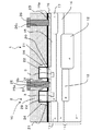
特許文献2に開示されている閾値電圧変調方式のMOSイメージセンサを、図6および図7を用いて説明する。
A threshold voltage modulation type MOS image sensor disclosed in
図6(a)および(b)は、それぞれ、閾値電圧変調方式のMOS型イメージセンサを製造するための各製造工程を示す概略断面図である。MOS型イメージセンサには、受光ダイオード(フォトダイオード)60およびMOSトランジスタ100が同一基板に設けられている。なお、以下の説明においては、受光ダイオード60およびMOSトランジスタ100における主要部についてのみ説明する。
6A and 6B are schematic cross-sectional views showing respective manufacturing steps for manufacturing a threshold voltage modulation type MOS image sensor. In the MOS image sensor, a light receiving diode (photodiode) 60 and a
図6(a)に示すように、従来の閾値電圧変調方式のMOS型イメージセンサは、p型エピタキシャル半導体層を含むシリコン基板50(以下、シリコン基板50)上に、フォトダイオード60に対応するn型不純物領域58と、このn型不純物領域58に隣接するp型不純物領域57とが形成されている。
As shown in FIG. 6A, a conventional threshold voltage modulation type MOS image sensor has an n corresponding to a
このシリコン基板50上には、p型不純物領域57およびn型不純物領域58を覆うように、n型層59が積層されており、このn型層59上には、p型不純物領域54およびn型低濃度不純物領域53が、p型不純物領域57およびn型不純物領域58に対応いる上方の領域に、その順番で積層されている。積層状態になったp型不純物領域54およびn型低濃度不純物領域53は、n型層59上に形成されたn型ウェル分離領域56にて囲まれた状態になっている。
An n-
各不純物領域が形成されたシリコン基板50には、シリコン基板50の表面の全面を覆うゲート絶縁膜51を形成した後に、このゲート絶縁膜51上に、MOSトランジスタ100におけるリング状のゲート電極52を、p型不純物領域54上におけるn型ウェル分離領域56に隣接する位置に形成する。n型低濃度不純物領域53の表面には、ゲート電極52のドライエッチング加工時の残膜として、ゲート絶縁膜51が残存している。
A
次に、図6(b)に示すように、ゲート電極52をマスクとし、また、ゲート絶縁膜51を注入保護膜として、イオン注入することにより、MOSトランジスタ100のソース領域およびドレイン領域となるn型不純物領域55を形成する。このとき、受光ダイオード60の領域では、p型不純物領域54の上面側にn型不純物領域55が形成されることにより、光発生電荷に対する埋め込み構造が形成される。このn型不純物領域55は、高濃度であり、しかも、シリコン基板50の表面から浅い位置に形成される。このように、受光ダイオード60の領域に、シリコン基板50の表面から浅い位置に高濃度のn型不純物領域55が形成されることにより、シリコン基板50の表面の近傍において急激に減衰するおそれのある短波長の青色光を、強度を減衰させることなく高強度で確実に受光することができる。
Next, as shown in FIG. 6 (b), by using the
このようにして作製された受光ダイオード60について、シリコン基板50の表面から深さ方向におけるn型不純物濃度分布を図7に示す。図7の縦軸は不純物濃度を示し、横軸は、シリコン基板50の表面からの距離(深さ)を示す。
FIG. 7 shows the n-type impurity concentration distribution in the depth direction from the surface of the
図7に示すように、n型不純物領域55は、シリコン基板50の表面から200nm(0.2μm)前後の深さ位置にまで形成されており、n型不純物領域55の不純物濃度のピーク位置は、基板表面から50nm以下の深さ位置になっている。
従来の閾値電圧変調方式のMOS型イメージセンサ100では、波長が短く、表面近くで急激に減衰してしまう青色光を、強度を減衰させることなく、高強度で確実に受光するために、受光ダイオード60の領域の表面において不純物濃度の領域を浅く(薄く)形成している。
In the conventional threshold voltage modulation type
しかしながら、ゲート電極52のドライエッチング加工時には、シリコン基板50の表面にゲート絶縁膜51が残存しており、その残存するゲート絶縁膜51の膜厚にばらつきがある。このため、受光ダイオード60表面部のn型不純物領域55をイオン注入により形成する場合に、注入保護膜となるゲート絶縁膜51の膜厚のばらつきによって、n型不純物領域55の不純物濃度のピーク位置にばらつきが生じ、受光ダイオード部60での光発生電荷に対する埋め込み耐性にばらつきが生じる。
However, when the
また、ゲート絶縁膜51は、ドライエッチング後において約300オングストローム程度の膜厚で残存する。受光ダイオード60の表面にn型不純物領域55を形成するためには低エネルギーでのイオン注入を行う必要があるが、このように、約300オングストローム程度のゲート絶縁膜51が存在すると、ゲート絶縁膜51の表面からシリコン基板50の表面までの距離が長くなり、イオンを注入する際のイオンの注入飛程のばらつき(ΔRp)が大きくなり、シリコン基板50の深さ方向に対する不純物領域の拡がりが大きくなるという問題がある。
The
また、イオン注入不純物の注入時における平均飛程を、シリコン基板50の表面から深い内部の位置に設定すると、受光ダイオード60部にも注入欠陥が発生して表面リーク電流が生じるおそれがある。
If the average range at the time of ion implantation impurity implantation is set at a position deep inside from the surface of the
さらに、ゲート電極52をプラズマ加工によって形成する場合には、プラズマによって受光ダイオード60の最表面にダメージが与えるられると、表面欠陥を原因とする表面リーク電流が生じるおそれもある。
Further, when the
本発明は、上記従来技術の課題を解決するものであり、受光領域におけるイオン注入によって生じる欠陥を低減し、受光領域の表面において光発生電荷による表面リーク電流を低減することができる固体撮像素子の製造方法を提供することを目的とする。
The present invention is intended to solve the above problems of the prior art, to reduce defects caused by ion implantation in the light receiving region, the solid-state imaging element capable of reducing the surface leakage current due to light-generated charges at the surface of the light receiving region It aims at providing the manufacturing method of.
本発明の固体撮像素子の製造方法は、光照射により信号電荷を発生させる受光領域と、該受光領域で発生した信号電荷に応じた信号を出力するトランジスタとをそれぞれ有する複数の単位画素部を二次元のアレイ状に形成する固体撮像素子の製造方法において、 第1導電型基板に形成された第2導電型半導体層上に、該受光領域を構成する第1導電型ウェル領域を形成する工程と、該第1導電型ウェル領域内に電荷蓄積領域を形成する工程と、該第1導電型基板の全面にわたってゲート絶縁膜を形成する工程と、該電荷蓄積領域の上方に該ゲート絶縁膜を介して該トランジスタのゲート電極を形成する工程と、該ゲート電極下以外のゲート絶縁膜を除去して、該第1導電型基板の表面に熱酸化により絶縁膜を形成する工程と、該熱酸化した絶縁膜をイオン注入の保護膜とし、かつ該ゲート電極をマスクとして用いて、イオン注入時の平均飛程が該熱酸化した絶縁膜の内部となるように、該第1導電型基板の全面に第2導電型不純物を導入して第2導電型高濃度拡散領域を、該ゲート電極が設けられている領域以外の該第1導電型ウェル領域を含む領域上の基板表層部に形成する工程とを有しており、該第2導電型高濃度拡散領域として、該第1導電型基板の深さ方向の不純物濃度極大部が該第1導電型基板の表面に形成されているものであり、そのことにより上記目的が達成される。
The manufacturing method of the solid-state imaging device of the present invention includes two unit pixel units each having a light receiving region that generates a signal charge by light irradiation and a transistor that outputs a signal corresponding to the signal charge generated in the light receiving region. Forming a first conductivity type well region constituting the light receiving region on a second conductivity type semiconductor layer formed on a first conductivity type substrate in a method of manufacturing a solid-state imaging device formed in a three-dimensional array; A step of forming a charge storage region in the first conductivity type well region, a step of forming a gate insulating film over the entire surface of the first conductivity type substrate, and a gate insulating film above the charge storage region. Forming a gate electrode of the transistor, removing a gate insulating film other than under the gate electrode, and forming an insulating film on the surface of the first conductivity type substrate by thermal oxidation, and performing the thermal oxidation Absolute Using the edge film as a protective film for ion implantation and the gate electrode as a mask, the entire surface of the first conductivity type substrate is placed so that the average range during ion implantation is inside the thermally oxidized insulating film . step of second conductivity type high concentration diffusion region by introducing a second conductivity type impurity to form formed on the substrate surface portion of the region including the first conductivity type well region other than the region where the gate electrode is provided and have a preparative, as the second conductivity type high concentration diffusion region, which impurity concentration maximum of the depth of the first conductivity type substrate is formed on the surface of the first conductivity type substrate This achieves the above object.
好ましくは、前記熱酸化した絶縁膜の膜厚を200オングストロームに設定する。
Preferably, it sets the thickness of the thermal oxidized insulating film 200 angstroms.
好ましくは、前記トランジスタが、MOSトランジスタである。 Preferably, the transistor is a MOS transistor.
好ましくは、前記第2導電型高濃度拡散領域は、前記第1導電型ウェル領域を含む領域として、該第1導電型ウェル領域上およびその外側を囲む分離領域上において、前記MOSトランジスタのドレイン領域であり、該MOSトランジスタに隣接する分離領域に近接した該第1導電型ウェル領域上において、該MOSトランジスタのソース領域である。Preferably, the second conductivity type high concentration diffusion region is a region including the first conductivity type well region, the drain region of the MOS transistor on the first conductivity type well region and on an isolation region surrounding the outside. The source region of the MOS transistor on the first conductivity type well region adjacent to the isolation region adjacent to the MOS transistor.
好ましくは、前記第2導電型高濃度拡散領域は、前記第1導電型ウェル領域を含む領域として、該第1導電型ウェル領域上およびその外側を囲む分離領域上において、前記MOSトランジスタのドレイン領域であり、該MOSトランジスタに隣接する分離領域に近接した該第1導電型ウェル領域上において、該MOSトランジスタのソース領域である。
Preferably, the second conductivity type high concentration diffusion region is a region including the first conductivity type well region, the drain region of the MOS transistor on the first conductivity type well region and on an isolation region surrounding the outside. The source region of the MOS transistor on the first conductivity type well region adjacent to the isolation region adjacent to the MOS transistor .
好ましくは、前記第1導電型ウェル領域のうち、前記受光領域を構成する第1導電型ウェル領域上を前記第2導電型高濃度拡散領域によって覆って埋め込み構造とする。 Preferably, the first conductive type well region of the first conductive type well region is covered with the second conductive type high concentration diffusion region to form a buried structure.
本発明によれば、受光領域、電荷蓄積領域およびトランジスタをそれぞれ備えた複数の単位画素部が二次元のアレイ状に設けられたMOS型イメージセンサなどの固体撮像素子において、受光領域において注入欠陥が発生することが低減され、表面リーク電流を低減することが可能となる。さらに、受光領域の第1導電型基板の表面では、第2導電型半導体層領域による表面発生リーク電流が低減されるために、第1導電型基板の表面より下方の第2導電型半導体層において、短波長である青色の感度向上を図
ることが可能となる。
According to the present invention, the light-receiving region, a charge storage region and a plurality of unit pixel sections having respective transistors Te solid-state image sensor odor such as a MOS type image sensor provided in a two-dimensional array, injected at the light receiving region The occurrence of defects is reduced, and the surface leakage current can be reduced. Furthermore, on the surface of the first conductive type substrate in the light receiving region, surface-generated leakage current due to the second conductive type semiconductor layer region is reduced, so that in the second conductive type semiconductor layer below the surface of the first conductive type substrate. Therefore, it is possible to improve the sensitivity of blue, which is a short wavelength.
また、本発明の固体撮像素子の製造方法では、基板表面を被覆するように熱酸化膜などの絶縁膜を、注入保護膜としてイオン注入を行って、受光領域表面の第2導電型半導体層領域を形成することにより、受光領域表面での表面欠陥を原因とする表面リーク電流を低減することができ、受光領域における特性を向上させることが可能となる。その結果、短波長である青色の感度向上を図ることが可能となる。 In the method for manufacturing a solid-state imaging device according to the present invention, ion implantation is performed using an insulating film such as a thermal oxide film as an implantation protective film so as to cover the substrate surface, and the second conductivity type semiconductor layer region on the surface of the light receiving region. By forming the surface leakage current due to surface defects on the surface of the light receiving region can be reduced, and the characteristics in the light receiving region can be improved. As a result, it is possible to improve the sensitivity of blue having a short wavelength.
以下に、本発明の固体撮像素子およびその製造方法を、閾値電圧変調方式のMOS型イメージセンサに適用した場合の実施形態について、図面を参照しながら説明する。なお、本発明の固体撮像素子は、MOS型イメージセンサに限定されるものではない。 Hereinafter, an embodiment in which the solid-state imaging device and the manufacturing method thereof according to the present invention are applied to a threshold voltage modulation type MOS image sensor will be described with reference to the drawings. The solid-state image sensor of the present invention is not limited to a MOS type image sensor.
図1は、本発明の固体撮像素子の一実施形態であるMOS型イメージセンサにおける単位画素部10のレイアウトの一例を示す平面図であり、図2は図1のA−A線に沿った断面図である。なお、図1および図2では、図示していないが、MOS型イメージセンサ(固体撮像素子)は、複数の単位画素部が行方向および列方向にマトリックス状(二次元アレイ状)に配置されている。
FIG. 1 is a plan view showing an example of a layout of a
図1および図2に示すMOS型イメージセンサの単位画素部10は、光電変換用の受光領域である受光ダイオード(フォトダイオード)1と、この受光ダイオード1に隣接して設けられた光信号検出用トランジスタのMOSトランジスタ2と、MOSトランジスタ2の下部に設けられた電荷蓄積用のキャリアポケット領域3(ホールポケット領域)とを有している。また、この単位画素部10とは行方向にそれぞれ隣接する単位画素部との間には、ゲート電極22の形成時に同時に作製される画素間分離電極28aおよび28bがそれぞれ設けられており、各画素間分離電極28aおよび28bによって、隣接する単位画素部10同士が分離されている。
A
図2に示すように、シリコン基板11には、光電変換用の受光ダイオード1の形成領域に、n型埋め込み層12が設けられており、受光ダイオード1の形成領域に隣接する光信号検出用のMOSトランジスタ2の形成領域には、n型埋め込み層12に隣接してp型埋め込み層13が設けられている。そして、n型埋め込み層12およびp型埋め込み層13を覆って、シリコン基板11の全面にn型層14が設けられている。
As shown in FIG. 2, the
n型層14上には、受光ダイオード1およびMOSトランジスタ2の各形成領域にそれぞれ設けられたn型埋め込み層12およびp型埋め込み層13の上方域にp型ウェル領域15が設けられている。このp型ウェル領域15は、n型ウェル分離領域17によって囲まれており、n型ウェル分離領域17によってp型ウェル領域15の形成範囲が規定されている。受光ダイオード1側に設けられたp型ウェル領域15によって、光照射による電荷発生領域の一部(受光領域)が光電変換部になっている。また、光信号検出用のMOSトランジスタ2側のp型ウェル領域15によって、MOSトランジスタ2のトランジスタ領域が構成されている。
On the n-
p型ウェル領域15およびn型ウェル分離領域17上には、MOSトランジスタ2のトランジスタ領域における一部領域を除いて、n型高濃度拡散領域16が設けられている。従って、受光ダイオード1における光電変換された信号電荷の発生領域であるp型ウェル領域15上にn型高濃度拡散領域16が設けられており、このn型高濃度拡散領域16によって、p型ウェル領域15は光発生電荷に対する埋め込み構造になっている。
An n-type high
n型高濃度拡散領域16は、受光トランジスタ1領域におけるp型ウェル領域15上およびp型ウェル領域15の外側を囲むn型ウェル分離領域17上において、MOSトランジスタ2のn型ドレイン領域16aになっており、また、MOSトランジスタ2に隣接するn型ウェル分離領域17に近接したp型ウェル領域15上において、MOSトランジスタ2のn型ソース領域16bになっている。p型ウェル領域15上におけるn型ソース領域16bの周囲のリング状の領域には、n型高濃度拡散領域16が設けられずに、n型チャネルドープ層20になっている。このn型チャネルドープ層20が、MOSトランジスタ2における電流担体が移動するチャネル領域になっている。
The n-type high
n型ドレイン領域16aは、その下に設けられたウェル分離領域17を介して、単位画素部10の全領域にわたって設けられたn型層14と電気的に接続された状態になっている。
The n-
p型ウェル領域15上においてn型ソース領域16bを取り囲んでリング状に設けられたn型チャネルドープ層20上には、ゲート絶縁膜21を介して、ゲート電極22がリング状に設けられている。ゲート絶縁膜21は、ゲート電極22の下方部分以外は除去されている。そして、シリコン基板11の表面であるn型高濃度拡散領域16上には、絶縁膜23が設けられており、この絶縁膜23は、シリコン基板11上に設けられたリング状のゲート電極22を覆っている。リング状のゲート電極22の側壁は、絶縁膜23を介して設けられたサイドウォール24によって覆われている。
On the p-
シリコン基板11上には、全面にわたって層間絶縁膜29が設けられており、この層間絶縁膜が、リング状のゲート電極22を覆う絶縁膜23およびサイドウォール24を覆っている。ゲート電極22の中央部に設けられたn型ソース領域16bは、層間絶縁膜29に設けられたソースコンタクトホール25aによってソース電極25に接続されている。また、リング状のゲート電極22は、層間絶縁膜29に設けられたゲートコンタクトホール27a(図1参照)によってゲート電極27と接続されている。さらに、n型ドレイン領域16aは、層間絶縁膜29に設けられたドレインコンタクトホール26aによってドレイン電極26と接続されている。
An interlayer insulating
p型ウェル領域15内には、電荷蓄積領域であるキャリアポケット領域としてホールポケット領域3が設けられている。ホールポケット領域3は、p型ウェル領域15よりも不純物濃度が高い高濃度埋込層として、n型ソース領域16bを囲むリング状に形成されている。リング状のホールポケット領域3は、その上方に設けられるリング状のゲート電極22に対して、ゲート電極22にて取り囲まれたソース電極25側(中心側)に近接した同心状態になっている。ホールポケット領域3内には、受光ダイオード1において光照射により発生した光信号キャリアである正孔(ホール)が蓄積されるようになっており、このホールポケット領域3内の光信号キャリアの蓄積量に比例してMOSトランジスタ2の閾値が変化するようになっている。
In the p-
このような構成のMOS型イメージセンサ10の動作を、以下に説明する。
The operation of the
本実施形態のMOS型イメージセンサ10(固体撮像素子)では、初期化(リセット)動作−電荷蓄積動作−信号読み出し動作という一連の動作が繰り返して行われる。 In the MOS image sensor 10 (solid-state imaging device) of the present embodiment, a series of operations including an initialization (reset) operation, a charge accumulation operation, and a signal readout operation are repeatedly performed.
まず、初期化動作期間には、ゲート電極22、ソース電極25およびドレイン電極26に正の高電圧が印加されてホールポケット領域3に残存する光信号キャリアがp型埋め込み層13を介してシリコン基板11の下部側に排出される。
First, during the initialization operation period, a positive high voltage is applied to the
次の電荷蓄積動作期間には、受光ダイオード1への光照射により発生した光信号キャリアであるホール(正孔)がp型ウェル領域15を介してゲート電極22下のホールポケット領域3内に蓄積される。
In the next charge accumulation operation period, holes (holes) that are optical signal carriers generated by light irradiation to the
そして、次の信号読み出し動作期間には、ホールポケット領域3への光信号キャリアの蓄積量に比例した信号がソース領域16bから出力されて、光電変換信号として検出される。
In the next signal readout operation period, a signal proportional to the amount of optical signal carriers accumulated in the
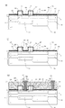
以下に、本実施形態のMOS型イメージセンサ10の製造方法について、図3A〜図3Cを用いて説明する。
Below, the manufacturing method of the MOS
図3A〜図3Cは、それぞれ、図1および図2のMOS型イメージセンサ10の各製造工程を示す断面図である。なお、この断面図は、図1のA−A線に沿った断面図に対応している。
3A to 3C are cross-sectional views showing respective manufacturing steps of the MOS
まず、図3A(a)に示すように、シリコン基板11の全面に酸化膜等の保護膜30を形成して、その保護膜30上にマスクパターン膜31を積層する。次いで、このマスクパターン膜31に、受光ダイオード1の形成領域に対応した開口部を形成し、その開口部からシリコン基板11に不純物を導入して、受光ダイオード1の形成領域に、ピーク不純物濃度約1×1017cm−3のn型埋め込み層12を、ピーク位置がシリコン基板11の表面から約1.5μmの深さの位置に形成する。
First, as shown in FIG. 3A (a), a
次に、図3A(b)に示すように、マスクパターン膜31を除去して、単位画素部10の領域全体にわたってn型不純物を導入することにより、受光ダイオード1のn型埋め込み層12上を覆うように、n型層14を形成する。n型層14は、ピーク不純物濃度が約3×1016cm−3、ピーク位置がシリコン基板11の表面から約0.7μmの深さになるように形成される。これにより、シリコン基板11には、n型埋め込み層12と、このn型埋め込み層12を覆って積層されたn型層14とが形成される。
Next, as shown in FIG. 3A (b), the
その後、画素間分離電極28aおよび28b(図1参照)の各領域上にマスクパターンを設けた状態で、シリコン基板11の全体にわたってp型不純物を導入し、n型層14上に接してp型ウェル領域15を形成し、そのp型ウェル領域15の表面側部分にn型不純物を導入してn型のチャネルドープ層20をシリコン基板11の全面に形成する。
Thereafter, p-type impurities are introduced over the
次に、図3A(c)に示すように、保護膜30上にマスクパターン膜32を積層して、光信号検出用のMOSトランジスタ2の形成領域に対応した開口部を形成し、この開口部から、n型不純物層14と同一深さ部分に、基板電位固定のためのp型不純物を導入して、n型不純物層14よりも不純物濃度が高いp型埋め込み層13を、n型埋め込み層12に隣接して形成する。
Next, as shown in FIG. 3A (c), a
その後、図3A(d)に示すように、相互に隣接して形成されたp型埋め込み層13およびn型埋め込み層12の上方域を覆うように、保護膜30上にマスクパターン33を設けて、p型埋め込み層13およびn型埋め込み層12の上方域以外の領域を開放した状態で、p型ウェル領域15におけるp型埋め込み層13およびn型埋め込み層12を取り囲む周囲の領域にn型不純物を導入して、p型ウェル領域15およびn型チャネルドープ層20を取り囲むn型ウェル分離領域17を形成する。これによって、p型ウェル領域15がウェル分離領域17によって分離されると共に、受光ダイオード1における光信号に対する感度を決定する受光領域が所定の面積で形成される。
Thereafter, as shown in FIG. 3A (d), a
続いて、図3B(e)に示すように、光信号検出用MOSトランジスタ2のp型ウェル領域15に形成されるホールポケット領域3に対応したリング状の開口部が形成されたマスクパターン膜34を絶縁膜30上に積層して、開口部から、MOSトランジスタ2のp型ウェル領域15内にp型不純物を導入する。これにより、p型ウェル領域15よりも不純物濃度が高く、ピーク不純物濃度が約1.4×1017cm−3のリング状のホールポケット領域3を、ピーク位置がシリコン基板11の表面から約0.15μmの深さになるように形成する。
Subsequently, as shown in FIG. 3B (e), a
次に、図示は省略するが、マスクパターン膜34を除去した後、シリコン基板11の全面にわたって表面を熱酸化してゲート絶縁膜21を形成する。
Next, although not shown, after removing the
その後、図3B(f)に示すように、ホールポケット領域3の上方域におけるゲート絶縁膜21上に、ホールポケット領域3の表面よりも広い面積でこのホールポケット領域3全体を覆うリング状のゲート電極22を形成する。リング状のゲート電極22は、リング状のホールポケット領域3と同心状態で、ゲート電極22の中心側にホールポケット領域3が接近した状態になるように形成される。
Thereafter, as shown in FIG. 3B (f), a ring-shaped gate covering the whole
次いで、図3B(g)に示すように、ゲート絶縁膜21をウェットエッチング加工によって除去して、p型ウェル領域15の表面およびウェル分離領域17の表面を露出させる。このとき、ゲート絶縁膜21は、ゲート電極22をマスクとしてエッチング除去されるために、ゲート電極22の下方においてのみ残存した状態になる。
Next, as shown in FIG. 3B (g), the
次に、図3B(h)に示すように、シリコン基板11の表面の全面にわたって800℃のドライO2酸化により熱酸化して絶縁膜23を形成する。このときの絶縁膜23の膜厚は約200オングストロームであり、p型基板11の全面における膜厚ばらつきは約5オングストローム以内に制御される。この場合、ゲート電極22の上面および側壁にも熱酸化膜23が形成されるが、この熱酸化膜23は、形成されるMOSトランジスタの特性には影響を与えず、また、ゲート電極22に側壁に形成されるサイドウォール加工時のプラズマダメージに対する保護膜としての機能も同時に果たす。
Next, as shown in FIG. 3B (h), the entire surface of the
続いて、図3C(i)に示すように、絶縁膜23をイオン注入の保護膜として、また、ゲート電極22をマスクとして、n型不純物をシリコン基板11の全面に導入して、n型高濃度拡散領域16を、ゲート電極22が設けられている領域以外のシリコン基板11の表層部に形成する。このとき、イオン注入時の平均飛程が絶縁膜23内部となるようにピーク不純物濃度は約6×1018cm−3とされ、n型不純物領域16の不純物濃度の極大部が、シリコン基板11の表面、すなわち、n型不純物領域16の表面になるようにされ、さらには、その濃度は約3×1018cm−3とされる。
Subsequently, as shown in FIG. 3C (i), an n-type impurity is introduced over the entire surface of the
次に、図3C(j)に示すように、サイドウォール用のSiO2などからなるシリコン酸化膜層をシリコン基板11の全面にわたって形成し、ドライエッチング加工により、ゲート電極22の側壁にサイドウォール膜24を形成する。
Next, as shown in FIG. 3C (j), a silicon oxide film layer made of SiO 2 or the like for the sidewall is formed over the entire surface of the
その後、図3C(k)に示すように、シリコン基板11の全面にわたって層間絶縁膜29を形成し、ソース領域16b、ドレイン領域16aおよびゲート電極22にそれぞれ対応するコンタクトホール25a、26aおよび27aを形成して、ソース電極25、ドレイン電極26およびゲート電極27を形成する。
Thereafter, as shown in FIG. 3C (k), an
これにより、本実施形態のMOS型イメージセンサが形成される。 Thereby, the MOS type image sensor of this embodiment is formed.
図4は、このようにして形成されたMOS型イメージセンサにおいて、受光ダイオード部1におけるシリコン基板11の表面から深さ方向に向かうn型不純物濃度分布を示すグラフである。図4の縦軸は不純物濃度を示し、横軸は基板表面から深さ方向の位置を示している。
FIG. 4 is a graph showing the n-type impurity concentration distribution in the depth direction from the surface of the
図4に示すように、本実施形態のMOS型イメージセンサでは、n型高濃度拡散領域16の厚さは100nm前後であり、n型高濃度拡散領域16の不純物濃度のピーク位置はシリコン基板の最表面になっている。
As shown in FIG. 4, in the MOS type image sensor of this embodiment, the thickness of the n-type high
図5は、n型高濃度拡散領域16を形成するための不純物注入工程において、注入されるイオンの平均飛程位置と表面発生リーク電流との関係を示すグラフである。図5の縦軸は表面リーク電流を示し、横軸は注入されるイオンの平均飛程位置(注入到達深さ)を示している。
FIG. 5 is a graph showing the relationship between the average range position of implanted ions and the surface-generated leakage current in the impurity implantation step for forming the n-type high
図5に示すように、平均飛程位置が絶縁膜23内部にあるときに表面発生リーク電流が極小値となっている。
As shown in FIG. 5, when the average range position is inside the insulating
以上のように、本実施形態によれば、受光領域である受光ダイオード(フォトダイオード)1と、電荷蓄積領域3を有するMOSトランジスタ2とを備えた複数の単位画素部10が二次元のアレイ状に設けられたMOS型イメージセンサにおいて、ゲート電極加工後に受光領域の表面を覆う絶縁膜(ゲート絶縁膜)21を一旦ウェットエッチングなどにより除去し、その後に、シリコン基板11の表面を被覆するように熱酸化膜からなる絶縁膜23を形成し、この絶縁膜23を注入保護膜としてイオン注入を行って、受光ダイオード部1の表面にn型高濃度拡散領域16を形成しているために、受光領域を被覆する膜絶縁膜23は、その膜厚のばらつきが、従来技術において、ゲート電極22の加工時にゲート絶縁膜を残すことによって発生するゲート絶縁膜の膜厚ばらつきと比較して、極めて小さくなり、また、絶縁膜23の膜厚自体も、従来技術に比べて薄くすることが可能であるため、イオン注入時におけるイオンの到達深さのばらつきによって発生する表面リーク電流のばらつきを極小化することができる。
As described above, according to the present embodiment, the plurality of
また、この絶縁膜23は、ゲート電極22加工時における受光領域のプラズマダメージを軽減させることができる膜としても機能するため、受光ダイオード1表面での表面欠陥を原因とする表面リーク電流を低減することもできる。
The insulating
さらに、受光ダイオードの1表面のn型不純物領域16を形成する際に、イオン注入不純物の注入平均飛程を絶縁膜23内に設定することにより、受光領域にイオンが注入されることによって発生する欠陥を低減することができる。また、受光領域におけるシリコン基板11の最表面からシリコン基板11の深さ方向に不純物濃度勾配を設けることが可能となり、シリコン基板11最表面ではn型高濃度拡散領域16による表面発生リーク電流を低減することができ、シリコン基板11の最表面より深い部分であるn型高濃度拡散領域16において、短波長の青色の感度を向上させることができる。
Further, when the n-
なお、本発明は、以上の実施形態に限定されるものではなく、同様な効果を得るために、上記実施形態において説明した各層および各領域の導電型を、n型基板上において全て逆転させて形成したものであってもよい。 The present invention is not limited to the above embodiment, and in order to obtain the same effect, the conductivity type of each layer and each region described in the above embodiment is reversed on the n-type substrate. It may be formed.
以上のように、本発明の好ましい実施形態を用いて本発明を例示してきたが、本発明は、この実施形態に限定して解釈されるべきものではない。本発明は、特許請求の範囲によってのみその範囲が解釈されるべきであることが理解される。当業者は、本発明の具体的な好ましい実施形態の記載から、本発明の記載および技術常識に基づいて等価な範囲を実施することができることが理解される。本明細書において引用した特許、特許出願および文献は、その内容自体が具体的に本明細書に記載されているのと同様にその内容が本明細書に対する参考として援用されるべきであることが理解される。 As mentioned above, although this invention has been illustrated using preferable embodiment of this invention, this invention should not be limited and limited to this embodiment. It is understood that the scope of the present invention should be construed only by the claims. It is understood that those skilled in the art can implement an equivalent range based on the description of the present invention and the common general technical knowledge from the description of specific preferred embodiments of the present invention. Patents, patent applications, and documents cited herein should be incorporated by reference in their entirety, as if the contents themselves were specifically described herein. Understood.
本発明は、例えばビデオカメラ、デジタルカメラ、カメラ付き携帯電話器などに用いられる閾値電圧変調方式のMOS型イメージセンサなどの固体撮像素子およびその製造方法の分野において、受光領域におけるイオン注入による欠陥の発生を低減することが可能となり、受光ダイオード表面での表面欠陥を原因とする表面リーク電流を低減することが可能になる。よって、本発明の固体撮像素子は、フォトダイオード特性が優れているため、ビデオカメラ、デジタルカメラ、カメラ付き携帯電話器など、固体撮像素子を利用可能な電子情報機器に幅広く利用することができる。 The present invention relates to defects caused by ion implantation in a light receiving region in the field of a solid-state imaging device such as a threshold voltage modulation type MOS image sensor used for, for example, a video camera, a digital camera, a mobile phone with a camera, and the like. Occurrence can be reduced, and surface leakage current caused by surface defects on the surface of the light receiving diode can be reduced. Therefore, since the solid-state imaging device of the present invention has excellent photodiode characteristics, it can be widely used in electronic information devices that can use the solid-state imaging device, such as video cameras, digital cameras, and camera-equipped mobile phones.
1 受光ダイオード(受光領域)
2 光信号検出用のMOSトランジスタ
3 ホールポケット領域
10 単位画素部
11 シリコン基板
12 n型層
13 p型埋め込み層
14 n型層
15 p型ウェル領域
16 n型高濃度拡散領域
16a n型ドレイン領域
16b n型ソース領域
17 ウェル分離領域
20 n型チャネルドープ層
21 ゲート絶縁膜
22 ゲート電極
23 絶縁膜
24 サイドウォール
25 ソース電極
25a、26a、27a コンタクトホール
26 ドレイン電極
28a、28b 画素間分離電極
29 層間絶縁膜
31〜34 マスクパターン
1 Light receiving diode (light receiving area)
2 MOS transistor for
Claims (6)
第1導電型基板に形成された第2導電型半導体層上に、該受光領域を構成する第1導電型ウェル領域を形成する工程と、
該第1導電型ウェル領域内に電荷蓄積領域を形成する工程と、
該第1導電型基板の全面にわたってゲート絶縁膜を形成する工程と、
該電荷蓄積領域の上方に該ゲート絶縁膜を介して該トランジスタのゲート電極を形成する工程と、
該ゲート電極下以外のゲート絶縁膜を除去して、該第1導電型基板の表面に熱酸化により絶縁膜を形成する工程と、
該熱酸化した絶縁膜をイオン注入の保護膜とし、かつ該ゲート電極をマスクとして用いて、イオン注入時の平均飛程が該熱酸化した絶縁膜の内部となるように、該第1導電型基板の全面に第2導電型不純物を導入して第2導電型高濃度拡散領域を、該ゲート電極が設けられている領域以外の該第1導電型ウェル領域を含む領域上の基板表層部に形成する工程とを有しており、
該第2導電型高濃度拡散領域として、該第1導電型基板の深さ方向の不純物濃度極大部が該第1導電型基板の表面に形成されている固体撮像素子の製造方法。 A solid-state imaging device in which a plurality of unit pixel portions each having a light receiving region that generates a signal charge by light irradiation and a transistor that outputs a signal corresponding to the signal charge generated in the light receiving region are formed in a two-dimensional array In the manufacturing method,
Forming a first conductivity type well region constituting the light receiving region on a second conductivity type semiconductor layer formed on the first conductivity type substrate;
Forming a charge storage region in the first conductivity type well region;
Forming a gate insulating film over the entire surface of the first conductivity type substrate;
Forming a gate electrode of the transistor above the charge storage region via the gate insulating film;
Removing a gate insulating film other than under the gate electrode and forming an insulating film on the surface of the first conductivity type substrate by thermal oxidation;
Using the thermally oxidized insulating film as a protective film for ion implantation and using the gate electrode as a mask , the first conductivity type is set so that the average range at the time of ion implantation is within the thermally oxidized insulating film . the entire surface by introducing second conductivity type impurities second conductivity type high concentration diffusion region of the substrate, the substrate surface layer portion of the region including the first conductivity type well region other than the region where the gate electrode is provided It has been closed and a step that form,
A method for manufacturing a solid-state imaging device, wherein the impurity concentration maximum portion in the depth direction of the first conductivity type substrate is formed on the surface of the first conductivity type substrate as the second conductivity type high concentration diffusion region .
7. The solid-state imaging device according to claim 6, wherein the first conductive type well region of the first conductive type well region is covered with the second conductive type high-concentration diffusion region to form a buried structure. Production method.
Priority Applications (4)
| Application Number | Priority Date | Filing Date | Title |
|---|---|---|---|
| JP2004107904A JP4004484B2 (en) | 2004-03-31 | 2004-03-31 | Manufacturing method of solid-state imaging device |
| KR1020050027134A KR100676284B1 (en) | 2004-03-31 | 2005-03-31 | Solid-state image sensor and method for fabricating the same |
| US11/096,925 US7304338B2 (en) | 2004-03-31 | 2005-03-31 | Solid-state image sensor and method for fabricating the same |
| TW094110370A TWI255040B (en) | 2004-03-31 | 2005-03-31 | Solid-state image sensor and method for fabricating the same |
Applications Claiming Priority (1)
| Application Number | Priority Date | Filing Date | Title |
|---|---|---|---|
| JP2004107904A JP4004484B2 (en) | 2004-03-31 | 2004-03-31 | Manufacturing method of solid-state imaging device |
Publications (2)
| Publication Number | Publication Date |
|---|---|
| JP2005294554A JP2005294554A (en) | 2005-10-20 |
| JP4004484B2 true JP4004484B2 (en) | 2007-11-07 |
Family
ID=35327143
Family Applications (1)
| Application Number | Title | Priority Date | Filing Date |
|---|---|---|---|
| JP2004107904A Expired - Fee Related JP4004484B2 (en) | 2004-03-31 | 2004-03-31 | Manufacturing method of solid-state imaging device |
Country Status (4)
| Country | Link |
|---|---|
| US (1) | US7304338B2 (en) |
| JP (1) | JP4004484B2 (en) |
| KR (1) | KR100676284B1 (en) |
| TW (1) | TWI255040B (en) |
Families Citing this family (17)
| Publication number | Priority date | Publication date | Assignee | Title |
|---|---|---|---|---|
| EP1702361A2 (en) * | 2003-12-17 | 2006-09-20 | Analog Devices, Inc. | Integrated circuit fuse and method of fabrication |
| KR101244571B1 (en) * | 2006-02-22 | 2013-03-26 | 삼성전자주식회사 | Novel ferrocene containing polymer and organic memory device comprising the same |
| US7642579B2 (en) * | 2006-03-06 | 2010-01-05 | Stmicroelectronics S.A. | Image sensor comprising pixels with one transistor |
| US20080217716A1 (en) * | 2007-03-09 | 2008-09-11 | Mauritzson Richard A | Imaging apparatus, method, and system having reduced dark current |
| US20080258187A1 (en) * | 2007-04-18 | 2008-10-23 | Ladd John W | Methods, systems and apparatuses for the design and use of imager sensors |
| US8257997B2 (en) * | 2007-10-17 | 2012-09-04 | Sifotonics Technologies (Usa) Inc. | Semiconductor photodetectors |
| KR100855403B1 (en) | 2007-11-27 | 2008-08-29 | 주식회사 동부하이텍 | Image sensor and method for manufacturing the same |
| KR100855404B1 (en) | 2007-12-21 | 2008-08-29 | 주식회사 동부하이텍 | Method for manufacturing an image sensor |
| US7833819B2 (en) * | 2008-07-23 | 2010-11-16 | Aptina Imaging Corporation | Method and apparatus for decreasing storage node parasitic charge in active pixel image sensors |
| JP5091886B2 (en) * | 2009-02-13 | 2012-12-05 | 浜松ホトニクス株式会社 | Image sensor |
| JP5271104B2 (en) * | 2009-02-13 | 2013-08-21 | 浜松ホトニクス株式会社 | Linear image sensor |
| US7977717B1 (en) * | 2009-02-25 | 2011-07-12 | ON Semiconductor Trading, Ltd | Pixel sensing circuit |
| JP6007524B2 (en) * | 2012-03-12 | 2016-10-12 | セイコーエプソン株式会社 | Solid-state imaging device |
| DE102013018789A1 (en) | 2012-11-29 | 2014-06-05 | Infineon Technologies Ag | Controlling light-generated charge carriers |
| US9147710B2 (en) | 2013-07-23 | 2015-09-29 | Taiwan Semiconductor Manufacturing Co., Ltd. | Photodiode gate dielectric protection layer |
| JP6595750B2 (en) * | 2014-03-14 | 2019-10-23 | キヤノン株式会社 | Solid-state imaging device and imaging system |
| JP6892221B2 (en) * | 2016-03-04 | 2021-06-23 | エイブリック株式会社 | Manufacturing method of semiconductor devices |
Family Cites Families (12)
| Publication number | Priority date | Publication date | Assignee | Title |
|---|---|---|---|---|
| JPS5369526A (en) | 1976-12-03 | 1978-06-21 | Hitachi Ltd | Solid pickup unit |
| JP2002026303A (en) | 1990-06-25 | 2002-01-25 | Matsushita Electric Ind Co Ltd | Manufacturing method of solid-state image pickup device |
| JP2928058B2 (en) | 1993-07-15 | 1999-07-28 | 松下電子工業株式会社 | Method for manufacturing solid-state imaging device |
| JP3516552B2 (en) | 1996-04-30 | 2004-04-05 | シャープ株式会社 | Manufacturing method of light receiving element |
| US6051857A (en) * | 1998-01-07 | 2000-04-18 | Innovision, Inc. | Solid-state imaging device and method of detecting optical signals using the same |
| JP3664968B2 (en) | 1999-12-01 | 2005-06-29 | イノテック株式会社 | Solid-state imaging device, manufacturing method thereof, and solid-state imaging device |
| TW494574B (en) * | 1999-12-01 | 2002-07-11 | Innotech Corp | Solid state imaging device, method of manufacturing the same, and solid state imaging system |
| TW483127B (en) * | 2000-01-07 | 2002-04-11 | Innotech Corp | Solid state imaging device and driving method thereof |
| US6950134B2 (en) * | 2000-02-22 | 2005-09-27 | Innotech Corporation | Method of preventing transfer and storage of non-optically generated charges in solid state imaging device |
| JP2001284568A (en) * | 2000-03-31 | 2001-10-12 | Sharp Corp | Solid image-pickup device |
| US6448596B1 (en) * | 2000-08-15 | 2002-09-10 | Innotech Corporation | Solid-state imaging device |
| KR20020052791A (en) | 2000-12-26 | 2002-07-04 | 박종섭 | Image sensor formation method capable of protecting surface of substrate |
-
2004
- 2004-03-31 JP JP2004107904A patent/JP4004484B2/en not_active Expired - Fee Related
-
2005
- 2005-03-31 US US11/096,925 patent/US7304338B2/en not_active Expired - Fee Related
- 2005-03-31 TW TW094110370A patent/TWI255040B/en not_active IP Right Cessation
- 2005-03-31 KR KR1020050027134A patent/KR100676284B1/en not_active IP Right Cessation
Also Published As
| Publication number | Publication date |
|---|---|
| TWI255040B (en) | 2006-05-11 |
| US20060086955A1 (en) | 2006-04-27 |
| JP2005294554A (en) | 2005-10-20 |
| KR20060045371A (en) | 2006-05-17 |
| US7304338B2 (en) | 2007-12-04 |
| TW200536116A (en) | 2005-11-01 |
| KR100676284B1 (en) | 2007-01-30 |
Similar Documents
| Publication | Publication Date | Title |
|---|---|---|
| KR100676284B1 (en) | Solid-state image sensor and method for fabricating the same | |
| JP6541080B2 (en) | Solid-state imaging device | |
| JP3840203B2 (en) | Solid-state imaging device and camera system using the solid-state imaging device | |
| US20220190022A1 (en) | Image sensors | |
| JP5100988B2 (en) | Image sensor and manufacturing method thereof | |
| KR100758321B1 (en) | Image sensor with embedded photodiode region and fabrication method thereof | |
| TWI332262B (en) | Method for manufacturing cmos image sensor using spacer etching barrier film | |
| US20070045668A1 (en) | Vertical anti-blooming control and cross-talk reduction for imagers | |
| KR20170084519A (en) | Image sensors | |
| JP2009277722A (en) | Solid state imaging device, and method of manufacturing the same | |
| JP4479729B2 (en) | Solid-state imaging device, electronic module, and electronic device | |
| JP2005268814A (en) | Solid state imaging device and camera system using the same | |
| JP4435063B2 (en) | Solid-state imaging device and camera system using the solid-state imaging device | |
| JP3664968B2 (en) | Solid-state imaging device, manufacturing method thereof, and solid-state imaging device | |
| JP5478871B2 (en) | Photoelectric conversion device, imaging system, and method of manufacturing photoelectric conversion device | |
| JP5241759B2 (en) | Solid-state imaging device | |
| KR102026310B1 (en) | Isolation structure and method for fabricating the same, image sensor having isolation structure | |
| US10170515B2 (en) | Implantation process for semiconductor device | |
| JP2010171042A (en) | Semiconductor device and method for manufacturing the same |
Legal Events
| Date | Code | Title | Description |
|---|---|---|---|
| A977 | Report on retrieval |
Free format text: JAPANESE INTERMEDIATE CODE: A971007 Effective date: 20070216 |
|
| A131 | Notification of reasons for refusal |
Free format text: JAPANESE INTERMEDIATE CODE: A131 Effective date: 20070220 |
|
| A521 | Request for written amendment filed |
Free format text: JAPANESE INTERMEDIATE CODE: A523 Effective date: 20070419 |
|
| A02 | Decision of refusal |
Free format text: JAPANESE INTERMEDIATE CODE: A02 Effective date: 20070514 |
|
| A521 | Request for written amendment filed |
Free format text: JAPANESE INTERMEDIATE CODE: A523 Effective date: 20070612 |
|
| A911 | Transfer to examiner for re-examination before appeal (zenchi) |
Free format text: JAPANESE INTERMEDIATE CODE: A911 Effective date: 20070802 |
|
| TRDD | Decision of grant or rejection written | ||
| A01 | Written decision to grant a patent or to grant a registration (utility model) |
Free format text: JAPANESE INTERMEDIATE CODE: A01 Effective date: 20070821 |
|
| A61 | First payment of annual fees (during grant procedure) |
Free format text: JAPANESE INTERMEDIATE CODE: A61 Effective date: 20070821 |
|
| R150 | Certificate of patent or registration of utility model |
Free format text: JAPANESE INTERMEDIATE CODE: R150 |
|
| FPAY | Renewal fee payment (event date is renewal date of database) |
Free format text: PAYMENT UNTIL: 20100831 Year of fee payment: 3 |
|
| FPAY | Renewal fee payment (event date is renewal date of database) |
Free format text: PAYMENT UNTIL: 20110831 Year of fee payment: 4 |
|
| FPAY | Renewal fee payment (event date is renewal date of database) |
Free format text: PAYMENT UNTIL: 20110831 Year of fee payment: 4 |
|
| FPAY | Renewal fee payment (event date is renewal date of database) |
Free format text: PAYMENT UNTIL: 20120831 Year of fee payment: 5 |
|
| LAPS | Cancellation because of no payment of annual fees |