JP3994809B2 - Electronic circuit component punching device and its supply reel replacement method - Google Patents
Electronic circuit component punching device and its supply reel replacement method Download PDFInfo
- Publication number
- JP3994809B2 JP3994809B2 JP2002200090A JP2002200090A JP3994809B2 JP 3994809 B2 JP3994809 B2 JP 3994809B2 JP 2002200090 A JP2002200090 A JP 2002200090A JP 2002200090 A JP2002200090 A JP 2002200090A JP 3994809 B2 JP3994809 B2 JP 3994809B2
- Authority
- JP
- Japan
- Prior art keywords
- tape
- supply reel
- electronic circuit
- supply
- reel
- Prior art date
- Legal status (The legal status is an assumption and is not a legal conclusion. Google has not performed a legal analysis and makes no representation as to the accuracy of the status listed.)
- Expired - Fee Related
Links
Images


Classifications
-
- H—ELECTRICITY
- H05—ELECTRIC TECHNIQUES NOT OTHERWISE PROVIDED FOR
- H05K—PRINTED CIRCUITS; CASINGS OR CONSTRUCTIONAL DETAILS OF ELECTRIC APPARATUS; MANUFACTURE OF ASSEMBLAGES OF ELECTRICAL COMPONENTS
- H05K13/00—Apparatus or processes specially adapted for manufacturing or adjusting assemblages of electric components
- H05K13/02—Feeding of components
- H05K13/0215—Interconnecting of containers, e.g. splicing of tapes
-
- H—ELECTRICITY
- H01—ELECTRIC ELEMENTS
- H01L—SEMICONDUCTOR DEVICES NOT COVERED BY CLASS H10
- H01L21/00—Processes or apparatus adapted for the manufacture or treatment of semiconductor or solid state devices or of parts thereof
- H01L21/02—Manufacture or treatment of semiconductor devices or of parts thereof
- H01L21/04—Manufacture or treatment of semiconductor devices or of parts thereof the devices having at least one potential-jump barrier or surface barrier, e.g. PN junction, depletion layer or carrier concentration layer
- H01L21/50—Assembly of semiconductor devices using processes or apparatus not provided for in a single one of the subgroups H01L21/06 - H01L21/326, e.g. sealing of a cap to a base of a container
-
- H—ELECTRICITY
- H05—ELECTRIC TECHNIQUES NOT OTHERWISE PROVIDED FOR
- H05K—PRINTED CIRCUITS; CASINGS OR CONSTRUCTIONAL DETAILS OF ELECTRIC APPARATUS; MANUFACTURE OF ASSEMBLAGES OF ELECTRICAL COMPONENTS
- H05K13/00—Apparatus or processes specially adapted for manufacturing or adjusting assemblages of electric components
- H05K13/04—Mounting of components, e.g. of leadless components
- H05K13/0417—Feeding with belts or tapes
-
- H—ELECTRICITY
- H01—ELECTRIC ELEMENTS
- H01L—SEMICONDUCTOR DEVICES NOT COVERED BY CLASS H10
- H01L23/00—Details of semiconductor or other solid state devices
- H01L23/48—Arrangements for conducting electric current to or from the solid state body in operation, e.g. leads, terminal arrangements ; Selection of materials therefor
- H01L23/488—Arrangements for conducting electric current to or from the solid state body in operation, e.g. leads, terminal arrangements ; Selection of materials therefor consisting of soldered or bonded constructions
- H01L23/498—Leads, i.e. metallisations or lead-frames on insulating substrates, e.g. chip carriers
- H01L23/4985—Flexible insulating substrates
-
- H—ELECTRICITY
- H01—ELECTRIC ELEMENTS
- H01L—SEMICONDUCTOR DEVICES NOT COVERED BY CLASS H10
- H01L2924/00—Indexing scheme for arrangements or methods for connecting or disconnecting semiconductor or solid-state bodies as covered by H01L24/00
- H01L2924/0001—Technical content checked by a classifier
- H01L2924/0002—Not covered by any one of groups H01L24/00, H01L24/00 and H01L2224/00
-
- H—ELECTRICITY
- H05—ELECTRIC TECHNIQUES NOT OTHERWISE PROVIDED FOR
- H05K—PRINTED CIRCUITS; CASINGS OR CONSTRUCTIONAL DETAILS OF ELECTRIC APPARATUS; MANUFACTURE OF ASSEMBLAGES OF ELECTRICAL COMPONENTS
- H05K1/00—Printed circuits
- H05K1/02—Details
- H05K1/03—Use of materials for the substrate
- H05K1/0393—Flexible materials
-
- H—ELECTRICITY
- H05—ELECTRIC TECHNIQUES NOT OTHERWISE PROVIDED FOR
- H05K—PRINTED CIRCUITS; CASINGS OR CONSTRUCTIONAL DETAILS OF ELECTRIC APPARATUS; MANUFACTURE OF ASSEMBLAGES OF ELECTRICAL COMPONENTS
- H05K3/00—Apparatus or processes for manufacturing printed circuits
- H05K3/0011—Working of insulating substrates or insulating layers
- H05K3/0044—Mechanical working of the substrate, e.g. drilling or punching
- H05K3/0052—Depaneling, i.e. dividing a panel into circuit boards; Working of the edges of circuit boards
-
- H—ELECTRICITY
- H05—ELECTRIC TECHNIQUES NOT OTHERWISE PROVIDED FOR
- H05K—PRINTED CIRCUITS; CASINGS OR CONSTRUCTIONAL DETAILS OF ELECTRIC APPARATUS; MANUFACTURE OF ASSEMBLAGES OF ELECTRICAL COMPONENTS
- H05K3/00—Apparatus or processes for manufacturing printed circuits
- H05K3/0097—Processing two or more printed circuits simultaneously, e.g. made from a common substrate, or temporarily stacked circuit boards
-
- Y—GENERAL TAGGING OF NEW TECHNOLOGICAL DEVELOPMENTS; GENERAL TAGGING OF CROSS-SECTIONAL TECHNOLOGIES SPANNING OVER SEVERAL SECTIONS OF THE IPC; TECHNICAL SUBJECTS COVERED BY FORMER USPC CROSS-REFERENCE ART COLLECTIONS [XRACs] AND DIGESTS
- Y10—TECHNICAL SUBJECTS COVERED BY FORMER USPC
- Y10T—TECHNICAL SUBJECTS COVERED BY FORMER US CLASSIFICATION
- Y10T83/00—Cutting
- Y10T83/889—Tool with either work holder or means to hold work supply
- Y10T83/896—Rotatable wound package supply
- Y10T83/902—Plural supply sources
-
- Y—GENERAL TAGGING OF NEW TECHNOLOGICAL DEVELOPMENTS; GENERAL TAGGING OF CROSS-SECTIONAL TECHNOLOGIES SPANNING OVER SEVERAL SECTIONS OF THE IPC; TECHNICAL SUBJECTS COVERED BY FORMER USPC CROSS-REFERENCE ART COLLECTIONS [XRACs] AND DIGESTS
- Y10—TECHNICAL SUBJECTS COVERED BY FORMER USPC
- Y10T—TECHNICAL SUBJECTS COVERED BY FORMER US CLASSIFICATION
- Y10T83/00—Cutting
- Y10T83/929—Tool or tool with support
- Y10T83/9411—Cutting couple type
- Y10T83/9423—Punching tool
- Y10T83/9425—Tool pair
Description
【0001】
【発明の属する技術分野】
本発明は、テープキャリアパッケージ(TCP)等、テープに一定のピッチ間隔をもって多数の電子回路部を設けた電子回路キャリア部を有するテープから、電子回路部品を打ち抜いて分離する電子回路部品の打ち抜き装置及びこの打ち抜き装置において、テープを供給する供給リールの交換方法に関するものである。
【0002】
【従来の技術】
電子回路部品、特にIC回路素子を回路基板に搭載する方式として、IC回路素子を直接回路基板上に搭載する方式と、IC回路素子を所定の配線パターン等を形成したフィルム基板に実装した電子回路部品を回路基板に搭載する方式とがある。後者の場合には、テープに一定のピッチ間隔となるように電子回路を形成しておき、この電子回路を打ち抜いて回路基板に搭載するのが一般的である。
【0003】
例えば、液晶パネルを構成するガラス基板にドライバICを実装する際に、ガラス基板の電極引き出し部にACFテープを貼り付けておき、このACFテープに打ち抜いた電子回路部品が実装されているフィルム基板を圧着することによって、フィルム基板側の配線とガラス基板の電極とを電気的に接合させるようにする。この搭載方式は、例えばTAB搭載方式、COF搭載方式等と呼ばれるものである。電子回路部品はテープに多数配列するように構成されることから、ガラス基板に搭載する直前にテープを打ち抜いて電子回路部品を分離して、この電子回路部品を真空吸着等の手段で取り出してガラス基板に搭載する。
【0004】
電子回路部品の打ち抜き装置は、テープ供給部と、打ち抜き部と、回収部とから構成され、テープ供給部には、電子回路キャリア部を有するテープを巻回した供給リールがセットされる。このテープ供給部から打ち抜き部を経てテープ回収部に至るテープの走行経路にはテープ送り手段が設けられており、このテープ送り手段でテープがピッチ送りされる。そして、このピッチ送りの間に、カッタユニットを有する打ち抜き手段が作動して、電子回路部品の打ち抜き、分離が行われる。このようにして電子回路部品が打ち抜かれる都度、ハンドリング手段によりガラス基板に搭載される。
【0005】
前述した打ち抜き装置において、テープ供給部から打ち抜き部までの間に所定の長さのテープ走行経路が存在する関係から、テープの電子回路キャリア部の前後において、少なくともこのテープ走行経路の長さに相当する分以上のリーダテープ部が連結されている。このリーダテープ部には電子回路はもうけられていない。従って、テープ供給部に供給リールがセットされると、まず先端側のリーダテープ部を引き出して、テープの走行経路に沿って打ち抜き部を通過した位置まで引き回す。ここで、打ち抜き部の前後にテープ送り手段が設けられる場合には、リーダテープ部の先端は、少なくとも打ち抜き部におけるテープの走行方向前方の位置にまで引き出してテープ送り手段に係合させる。また、テープの最後の電子回路部が打ち抜き部に至り、それが打ち抜かれると、この供給リールによるテープの供給が終了するが、この最後の電子回路部が打ち抜かれる際にも、なおテープの後端部は供給リールに巻回した状態を保たせるために、テープの電子回路キャリア部の後端部にも所定長さのリーダテープ部を備えている。
【0006】
【発明が解決しようとする課題】
前述した打ち抜き装置によって電子回路部品の打ち抜きを継続して、供給リールに巻回したテープが使い切られた後にも、電子回路部品の供給を継続するために、新たな供給リールがテープ供給部にセットされる。この供給リールの交換作業は次の手順で行われる。
【0007】
まず、使用中の供給リールにおいて、最後の電子回路部が打ち抜かれた後、この供給リールに巻回されている後端側のリーダテープ部の末端が打ち抜き部を通過させるまで空送りを行う。その後に、供給リールを交換して、新たな供給リールがその支軸にセットされると、その先端側のリーダテープ部を供給リールから引き出して、テープ走行経路に沿って所定の位置まで引き回し、その後に最初の電子回路が設けられている部位が打ち抜き部の位置まで送り出されるように空送りを行う。
【0008】
ここで、供給リールの交換作業は、従来、作業者による手作業で行うようになっており、作業が面倒でもあり、また長時間を必要とする。しかも、供給リールの交換作業を行っている間は、当然、ガラス基板への電子回路部品の搭載が中断するために、時間的な無駄が生じることになる。さらに、作業者は供給リールのテープが使い切るタイミングを見計らって、最後の電子回路部が打ち抜かれた後に速やかに供給リールの交換作業に入らなければ、さらに時間的なロスが大きくなってしまう。従って、この時間的なロスを最小限に抑制するためには、作業者は供給リールの使い切り前からある時間だけ供給リールの交換のために待機しなければならず、この待機時間の間は作業者が他の作業を行えないことになり、その分だけ作業者による作業効率が悪くなってしまう。
【0009】
特に、近年においては、電子回路部品の自動搭載装置の進歩、改良等の結果、電子回路部品搭載のタクトタイムが速くなる傾向にあり、このために供給リールにおけるテープの使い切り時間が短く、つまり供給リールの交換頻度が高くなる傾向にあり、電子回路部品の搭載時間を短縮するために、このリール交換時間の短縮を図る必要性は極めて高いものとなっている。
【0010】
本発明は以上の点に鑑みてなされたものであって、その目的とするところは、作業者による供給リールの交換作業のタイミングを供給リールから最後の電子回路部が打ち抜かれる時点に拘束されないようになし、かつ迅速で容易な供給リール交換作業を可能にすることにある。
【0011】
【課題を解決するための手段】
前述した目的を達成するために、本発明による電子回路部品の打ち抜き装置の構成の特徴としては、一定のピッチ間隔で電子回路を形成した電子回路キャリア部と、この電子回路キャリア部の前後に設けられ、電子回路が形成されていないリーダテープ部とを有するテープが巻回された供給リールがセットされるテープ供給部と、このテープの電子回路を打ち抜いて電子回路部品をテープから分離する打ち抜き部とを備えた電子回路部品の打ち抜き装置であって、前記テープ供給部には、前記供給リールが着脱可能に装着されるリール装着部が少なくとも2箇所設けられ、前記テープにはスプロケット孔が設けられ、このスプロケット孔と係合するテープ送り手段により前記テープ供給部の一方の供給リールから前記打ち抜き部へのテープ走行経路に沿って前記テープを送る構成となし、前記打ち抜き部より上流側の位置に前記テープの電子回路を検出する検出手段を配置して、この検出手段の検出信号に基づいて前記打ち抜き部で前記電子回路部品を打ち抜くようになし、前記一方の供給リールからテープが供給されている間は他方の供給リールを待機させ、この待機中のテープの先端側リーダテープ部と係脱可能に保持させ、このリーダテープ部と使用中の供給リールの後端側リーダテープ部とがそれらのスプロケット孔の間隔が一致するように連結して、待機中の供給リールからテープを供給するように切り換える経路切換手段を備え、前記経路切換手段は、前記使用中の供給リールから送り出された後端側リーダテープ部の位置を切断する切断手段と、この切断手段により切断されたテープ後端を保持して待機中のテープの先端部分と所定長さ重ね合わせるためのテープ保持手段と、両テープを固着するテープ連結手段とを含むようにした点にある。
【0012】
要するに、1個の供給リールからテープの送り出しが開始した後、この供給リールのテープが使い切られる前まではいつでも、待機させる供給リールのセットが可能となる。従って、供給リールの交換のタイミングを計るように作業者自身が待機する必要がなくなる。ここで、テープ供給部から打ち抜き部までのテープ走行経路の途中に、使用中の供給リールから供給されるテープの最後に打ち抜かれる電子回路部の位置を検出する終端検出手段を設け、この終端検出手段からの信号に基づいて経路切換手段を作動させる構成とすれば、供給リールの交換のために、打ち抜き装置の中断時間は最小限に抑制できる。供給リールから供給されるテープにあっては、その電子回路キャリア部の両端に電子回路部が設けられていないリーダテープ部を設けるのが一般的である。そこで、経路切換手段は、使用中の供給リールから最後に送り出される後端側リーダテープ部を切断する切断手段と、切断されたテープ端を、保持部材に保持されている待機中の供給リールからのリーダテープ部の先端と重ね合わせるために、それぞれのテープを係脱可能に保持するテープ保持手段と、これら重ね合わせた両テープ端を連結する連結手段とを備える構成とする。供給リールにおける後端側のリーダテープ部を途中で切断され、かつ待機中の供給リールの先端側のリーダテープ部の大半を予め切断して除去できるので、かなりの長さ分の空送りが必要でなくなり、この空送り長さを短縮したことにより、さらに装置の稼動効率を向上させることができる。
【0013】
また、テープ供給部にセットされ、一定のピッチ間隔で電子回路部を形成した電子回路キャリア部と、この電子回路キャリア部の前後に設けられ、電子回路が形成されていないリーダテープ部とを有するテープが巻回された供給リールから供給されるテープを打ち抜き部で電子回路部を打ち抜いて電子回路部品をテープから分離する装置において、1つの供給リールからのテープが使い切られた後に、新たな供給リールからテープを供給できるように供給リールを交換する方法についての発明は、1つの供給リールからテープの供給が行われている間に、前記テープ供給部に新たな供給リールをセットして、この新たな供給リールのテープ先端を経路切換手段に接続し、前記1つの供給リールのテープが使い切られたことを検出したときに、経路切換手段によって、待機中のテープの他方の供給リールにおける先端側リーダテープ部と使用中の供給リールの後端側リーダテープ部とのスプロケット孔の間隔を一致させて、使用済みのテープの送り方向の後方部を切断し、この切断したテープ後端を保持させて待機中のテープの先端部分と所定長さ重ね合わせて、供給中のテープに新たな供給リールからの待機しているテープを連結・固着することをその特徴とするものである。
さらに、フィルム基板に形成した配線パターンにIC回路素子からなる電子部品を搭載した電子回路部品を製造する方法としては、テープ供給部に2箇所設けたリール支軸のそれぞれに、配線パターンが形成され、かつこれらの配線パターンに電子部品を接続した電子回路部を一定のピッチ間隔で形成され、この電子回路キャリア部の前後に電子回路が設けられていないリーダテープ部を連結して設けたテープを巻回した供給リールをセットし、これら2つの供給リールのうち、一方の供給リールから打ち抜き部にテープをピッチ送りする間に、センサにより前記電子部品を検出し、かつ前記電子回路部をこの打ち抜き部で位置決めした後、この打ち抜き部に設けたカッタを作動させて、前記電子部品部毎に打ち抜くことにより前記電子回路部品を順次前記テープから分離して取り出し、この一方の供給リールから供給されたテープが使い切られたことを前記センサで検出したときに、経路切換手段によって、待機中のテープの他方の供給リールにおける先端側リーダテープ部と使用中の供給リールの後端側リーダテープ部とのスプロケット孔の間隔を一致させて、使用済みのテープの送り方向の後方部を切断し、この切断したテープ後端を保持させて待機中のテープの先端部分と所定長さ重ね合わせて、供給中のテープに新たな供給リールからの待機しているテープを連結・固着して、この他方の供給リールから供給されたテープからの電子回路部が前記打ち抜き部に供給されたときに、前記電子回路部品の打ち抜きを開始し、この他方の供給リールでの電子回路部品の打ち抜きを行っている間に、テープが使い切られた前記一方の供給リールを新たな供給リールと交換することを特徴としている。
【0014】
【発明の実施の形態】
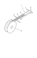
以下、図面を参照して、本発明の実施の形態について説明する。まず、図1にテープの構成の一例を示す。テープ1は多数の電子回路2を形成した電子回路キャリアテープ部1aを有し、電子回路2は、IC等の電子部品2aをテープ表面に印刷等の手段で形成した配線パターン2bに接続するように実装したものである。そして、同図に点線で示した切断線に沿って打ち抜くことによって、電子回路部品がテープ1から分離される。テープ1は、図2に示したように、リール3に巻回して設けられており、このリール3から繰り出すようにして供給されることになる。ここで、テープ1をリール3に巻回するに当っては、電子部品2aを保護するために、後述するセパレータテープを間に介在させて巻回させることになる。
【0015】
テープ1の左右両側には、一定のピッチ間隔をもって多数のスプロケット孔4が穿設されており、このスプロケット孔4に駆動スプロケットの爪を係合させて、この駆動スプロケットを回転駆動させることによって、テープ1をその走行経路に沿って連続的に走行させたり、またピッチ送りを行ったりすることができる。また、テープ1を構成する電子回路キャリアテープ部1aの前後にはリーダテープ部1b,1cが連設されている。なお、図2には先端側のリーダテープ部1bが表れているが、後端側のリーダテープ部1cはリール3のコアから所定の長さ分巻き付けられており、図面上では表れない。これらリーダテープ部1b,1cは、電子回路2は設けられていないが、スプロケット孔4は、電子回路キャリア部1aに連なるようにして設けられている。
【0016】
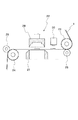
図3に電子回路部品の打ち抜き装置の構成を示す。図中において、11はテープ供給部、12は打ち抜き部、13は回収部である。テープ供給部11にはテープ1を巻回させた供給リール14が着脱可能に装着されるリール支軸15が設けられている。供給リール14には、テープ1がセパレータテープ5と重ね合わせるようにして巻回されている。また、テープ回収部13には、打ち抜き後のテープとセパレータテープ5とをそれぞれ回収する回収ボックス16,17が設置されている。
【0017】
ここで、図3から明らかなように、テープ供給部11には、2個の供給リール14(図には、両者を区別するために、それぞれに符号14A,14Bが付されている)が装着されるようになっており、このためにリール支軸15が2箇所設けられている。これら供給リール14は、その一方(図3の状態では供給リール14A)が使用中、つまり現にテープ1が供給されるものであり、このときには他方(図3の状態では供給リール14B)は待機状態となる。そして、使用中の供給リール14Aのテープ1が使い切られたときに、待機中の供給リール14Bからのテープ1が供給できる状態に迅速に移行させることによって、供給リールの交換時間を短縮し、かつ作業者による供給リールの交換作業を使用中の供給リールが使い切る時点に拘束されないようにするためである。このために、使用中の供給リールのテープ1が使い切られる時点を正確に検出して、待機している供給リールに供給経路の切り換えを行う。ここで、テープ1が使い切られたときとは、テープ1における電子回路キャリアテープ部1aに設けた電子回路2が全て打ち抜かれた状態をいう。
【0018】
このために、テープ供給部11から打ち抜き部12に至るテープ走行経路の途中であって、テープ供給部11に近接した位置に経路切換部20が設けられており、2個の供給リール14から供給されるテープ1は、この経路切換部20を通って打ち抜き部12に至るようにテープ1の走行経路が設定されている。このために、経路切換部20から打ち抜き部12に至るテープ走行経路には、適宜の位置に配置されたガイドローラ21にガイドさせてテープ1を引き回すようにしている。
【0019】
打ち抜き部12は、図4にも示したように、カッタユニット22と、このカッタユニット22の前後に設けたテープの送り駆動用のスプロケット23,24を有するピッチ送り手段とから構成される。スプロケット23,24の外周面にはテープ1に設けたスプロケット孔4に係合する爪が設けられている。また、これらスプロケット23,24にはテープ1の浮き上がり等を防止するためのピンチローラ25,26がテープ1に当接されるように設けられている。従って、テープ1は、これら両スプロケット23,24間では、実質的に水平状態に保たれ、かつ所定の張りを持たせることができるようになっている。そして、スプロケット23,24を間欠的に所定角度ずつ回転駆動することによって、テープ1が所定長さずつピッチ送りされるようになっている。
【0020】
カッタユニット22は、下部側の固定刃27と上部側の可動刃28とから構成され、可動刃28はソレノイド等からなるカッタ駆動手段29によって、上下動されるようになっている。従って、可動刃29が下降する毎にテープ1が切断されて、電子回路2の部分がキャリアテープ1から打ち抜かれて、電子回路部品が形成される。カッタユニット22の作動は、テープ走行経路におけるこのカッタユニット22の配設位置より上流側、好ましくはその直前、つまりスプロケット23とカッタユニット22との間の位置に設けられ、テープ1における電子部品2aを検出するセンサ30からの信号に基づいてなされる。
【0021】
電子回路2が打ち抜かれた後のテープはテープ回収ボックス16に回収されることになる。また、テープ1と共に供給リール14に巻回されているセパレータテープ5は、経路切換部20の位置より手前でテープ1から離れて、ガイド板31にガイドされて、回収ボックス17に回収されるようになっている。なお、セパレータテープ5は、回収ボックス17に回収させるのではなく、供給リール14とは異なるリールに巻回させるようにして回収し、供給リール14のテープ1を使い切った後に、この供給リール14に巻き戻すようにすることもできる。
【0022】
前述した2個の供給リールの取付位置、これらの供給リールからのテープ走行経路は、図示したものに限定されず、様々なレイアウトが可能である。図示したものにあっては、2個の供給リールは上下に配置されているが、例えば左右に配置することもできる。ただし、2個の供給リールからのテープ走行経路は、経路切換部20を設けた位置で合流しなければならない。また、打ち抜いた後のテープ及びセパレータテープは同じ回収ボックスで回収することもでき、あるいはリールに巻き取る等により回収するように構成することができる。
【0023】
今、1個の供給リール14、例えば図2にあるように、上部側に位置する方が使用中の供給リール14Aであり、つまりこの供給リール14Aから供給されるテープ1は打ち抜き部12から回収部16まで引き出されている。この状態で、テープ1は間欠送りされて、電子回路2毎に切断されるが、テープ1のピッチ送りは、打ち抜き部12において、カッタユニット22の前後に配置したスプロケット23,24をそれぞれ独立の(または共用の)モータで駆動されるようになっている。
【0024】
従って、テープ1の電子部品2aを検出するセンサ30の検出信号に基づいて、スプロケット23,24によりテープ1を1ピッチ分走行させ、カッタユニット22を構成する可動刃28を下降させることによって、この可動刃28と固定刃27とによりテープ1における電子回路2が打ち抜かれて電子回路部品が得られる。このようにして得られた電子回路部品は、例えば真空吸着手段等により取り出される。このようにして、電子回路2が取り出された後に、テープ1が1ピッチ分走行して、カッタユニット22を作動させる。これによって、順次電子回路2が打ち抜かれる。
【0025】
そして、供給リール14Aから供給されるテープ1が使い切られると、つまり最後の電子回路2が打ち抜かれると、もう一方のリール支軸15に装着されている供給リール14Bからテープ1の供給を開始する。このために、供給リール14Aのテープ1が使い切られる前までに供給リール14Bをセットしておく。そして、供給リール14Aに巻回されているテープ1における後端側のリーダテープ部1cに、供給リール14Bのテープ1における先端側のリーダテープ1bを継ぎ合わせし、供給リール14A側のリーダテープ部1cを、その継ぎ合わせた部位より後方の部分を切断する。これによって、待機していた供給リール14Bに巻回されているテープ1が打ち抜き部12に供給されるようになる。
【0026】
テープの繋ぎ及び切断は、経路切換部20により自動的に行わせるようにしている。そこで、図5に基づいて、この経路切換部20の具体的な構成の一例を説明する。なお、図5の状態では、上部側が使用中の供給リール14Aであり、下部側が待機中の供給リール14Bである。
【0027】
経路切換部20は、テープ1の走行経路Rを中心として上部側の上部構造部40Uと下部側の下部構造部40Lとから構成される。これら上部構造部40U,下部構造部40Lはそれぞれテープ保持部材41U,41Lとローラ42U,42Lとを含むものである。テープ保持部材41Uの下面には供給リール14Aから供給されるテープ1のリーダテープ部が吸着・保持される吸着孔43Uが少なくとも2箇所開口しており、また供給リール14Bから供給されるテープ1のリーダテープ部はテープ保持部材41Lの上面に吸着・保持される吸着孔43Lが少なくとも2箇所開口している。
【0028】
テープ保持部材41U,41Lはテープ走行方向に所定の長さを有するものであり、テープ走行方向の前方側の領域Fはテープ末端部を保持し、またテープ走行方向の後方側の領域Bはテープ先端部を保持するものである。そして、テープ保持部材41U,41Lの各領域F,Bには、それぞれ左右に各一対、つまり各々4本の位置決めピン44が設けられている。位置決めピン44はリーダテープ部のスプロケット孔4に係入するものであり、位置決めピン44は先端が尖った呼び込み部を有するものである。また、各領域F,Bに設けた位置決めピン44の前後の間隔はスプロケット孔4の間隔の整数倍に相当するものとなっている。しかも、上下のテープ保持部材41U,41Lに設けた位置決めピン44は相互にスプロケット孔4の1個または複数個の間隔分だけずれた位置に配置されている。
【0029】
さらに、上部側のテープ保持部材41Uには、テープ末端部を保持する領域Fとテープ先端部を保持する領域Bとの間の位置に、切断刃とその駆動手段とからなるカッタ45が設けられており、また下部側のテープ保持部材41L側にはカッタ45の切断刃が接離するカッタ受け45aが形成されている。さらにまた、下部側のテープ保持部材41Lには、領域F,Bには一方側のテープ末端部と他方側のテープ先端部とを連結するための針供給マガジン46aF,46aBと、作動部材46bF,46bBとからなるステープラ機構46F,46Bが装着されている。このステープラ機構46F,46Bは待機中のテープ1の先端を使用中のテープ1に連結するテープ連結手段を構成するものであり、このテープ連結手段の構成としては、ステープラによる止着の他に粘着テープ、熱圧着テープ等各種の手段を用いることができ、また止着と他の固着手段とを複合的に使用することも可能である。
【0030】
図5において、テープ1の走行経路Rの上下に配置されている上部側及び下部側の各テープ保持部材41U,41Lと、ローラ42U,42Lとは、走行経路Rに臨む位置と、この走行経路Rの上下で、この走行経路Rを走行するテープ1とは干渉しない位置とに変位可能となっている。また、テープ保持部材41U,41Lはその長さ方向の概略半ピッチ分前後方向に移動可能となっている。従って、ローラ42Uのみが走行経路Rに臨んでいると、供給リール14Aから供給されるテープ1が走行可能となり、ローラ42Lのみが走行経路Rに臨むと、供給リール14Bからのテープ1が走行可能となる。そして、テープ保持部材41U,41Lが対面する位置で、走行経路Rに臨むように接合され、カッタ45を作動させると、走行中のテープ1が切断される。また、テープ保持部材41U,41Lの一方が相手方に対して半ピッチ分ずらせた状態で、相互に接合させ、ステープラ46Fまたは46Bを作動させると、使用中のテープ1と待機中のテープ1とが連結されることになる。
【0031】
以上の構成を有する経路切換部20を設けることによって、1個の供給リール14からテープ1を供給する間の任意の時点で、もう一方のリール支軸15に新たな供給リール14をセットすることによって、使用中の供給リール14のテープ1が使い切られると、待機している供給リール14からのテープ1による供給が自動的に継続させることができる。しかも、使用中の供給リールから待機中の供給リールへの移行は、円滑かつ迅速に行なわれるようになる。
【0032】
今、図3に示したように、供給リール14Aからのテープ1が打ち抜き部12に供給されて、電子回路2の打ち抜きが実行されているとする。この供給リール14Aでのテープ1の供給が開始した後、このテープ1が使い切られる前までに、供給リール14Bのセットを行うことができる。この供給リール14Bのセットは作業者が手作業で行うことになる。供給リール14Aからのテープ1の供給が始まったときに、もう一つのリール支軸15に使い切られた供給リールが装着されていると、それを取り外した後に、このリール支軸15に新たな供給リール14Bを装着する。そして、この供給リール14Bからテープ1を引き出して、経路切換部20に設けた下部構造部40Lを構成するテープ保持部材41Lの領域B側の位置決めピン44にテープ1の先端部分のスプロケット孔4を係入させる。このテープ1の先端部は吸着孔43Lにより吸着保持される。
【0033】
これが図6に示した状態であって、供給リールをセットするに当って作業者が関与するのはこの作業だけであり、テープ1をその走行経路に沿って引き回す等といった面倒な作業は必要としない。
【0034】
ここで、供給リール14Bに巻回されているテープ1において、電子回路キャリアテープ部1aの先端にかなりの長さのリーダテープ部1bが連設されている。テープ保持部材41Lに保持させるのは、このリーダテープ部1bの先端であっても良いが、そうすると経路が切り換えられた後におけるテープ1の空送り距離が長くなる。従って、供給リール14Bからテープ1を引き出し、リーダテープ部1bの大半を切り取って、電子回路キャリアテープ部1aへの接続部に近い位置をテープ保持部材41Lに保持させる。これによって、使用中の供給リール14Aのテープ1が使い切られると、より迅速に供給リール14Bからテープ1が供給できる状態に切り換わる。
【0035】
作業者は、打ち抜き装置による電子回路部品の打ち抜きの進行状況とは無関係に、任意の時期に待機すべき供給リール14Bをセットすることができ、かつセットに要する時間も短縮されるので、作業者による作業性が極めて優れたものとなる。待機させるべき供給リール14Bがセットされている間及びその後にも、使用中の供給リール14Aからはテープ1の供給が継続される。打ち抜き部12へのテープ1の供給はセンサ30により常時検出されている。センサ30は電子回路2を構成する電子部品2aまたはその他の特徴を検出しており、このセンサ30により電子回路2が検出されなくなったとき、つまり供給リール14Aからのテープ1のうち、電子回路キャリアテープ部1aが打ち抜き部12を完全に通過したことが検出されると、この信号が経路切換部20に取り込まれて、テープ1の供給経路を、供給リール14A側から供給リール14B側に切り換える。従って、センサ30が末端検出手段を構成する。
【0036】
この切換動作は、まずテープ保持部材41Uを下降させ、またテープ保持部材41Lを上昇させて、図7に示したように、これら両テープ保持部材41U,41Lを接合させる。また、テープ保持部材41Lの上昇と連動させて、ローラ42Lを上昇させる。ここで、供給リール14Aからの使用中のテープ1は走行経路に沿って延在されているので、このテープ1のスプロケット孔4にテープ保持部材41U,41Lの位置決めピン44が係入する。ただし、位置決めピン44と使用中のテープ1のスプロケット孔4とが一致していない場合もある。しかしながら、位置決めピン44は先端が尖った呼び込み部となっているので、多少のずれがあっても、テープ1の位置が調整される。また、テープ1のスプロケット孔4に対して位置決めピン44が完全にずれている場合には、テープ1の送り駆動を行うスプロケット23,24を適宜回動させて、テープ1の位置調整を行う。
【0037】
待機中のテープ1の先端部分は、テープ保持部材41Lにおける領域Bの位置決めピン44に係入しているので、待機状態のテープ1と、使用中のテープ1とのスプロケット孔4が一致した状態となる。この状態で、カッタ45を作動させることによって、使用中のテープ1が切断されることになる。待機中のテープ1は領域B側にしか載置されていないので、この待機中のテープ1が切断されることはない。勿論、待機中のテープ1の先端が多少はみ出しており、カッタ45の作動により待機中のテープ1の先端部分が切断されたとしても、何等の問題も生じない。
【0038】
このテープ1の切断によりテープ保持部材41U側ではその領域Fの位置において、吸着孔43Uからの吸着力によりテープ1の後端部が保持される。切断後の供給リール側のテープ1は位置決めピン44に係入状態を保っているが、この段階で、位置決めピン44から強制的に離脱させて、供給リール14Aに巻き取るようにしても良い。ただし、新たな供給リールがセットされるまで、テープ保持部材41Uに保持させたまま維持することもできる。
【0039】
次に、図8に示したように、テープ保持材41Uを走行経路Rから離間させる方向に変位させる。そして、図9に示したように、テープ保持部材41Lを前進させて、テープ保持部材41Lの領域Bをテープ保持部材41Uの領域Fと一致させる位置まで変位させる。そして、テープ保持部材41Uを下降させて、図10に示したように、供給リール14A側からのテープ1の切断後端部に、供給リール14Bからのテープ1の先端が所定の長さ分だけオーバーラップされる。この状態で、ステープラ46Bを作動させて、両テープ1,1間を止着し連結する。テープ1,1間の連結が行われると、図10に示したように、ローラ42Lを走行経路Rに臨む状態とし、テープ保持部材41U,41L及びローラ42Uを走行経路Rから離間させる。これによって、供給リール14Bからテープ1が打ち抜き部12に供給される状態に切り換わる。そして、テープ1を高速送りして、センサ30が装着されている部位までテープ1を送ることによって、供給リール14B側のテープ1の電子回路キャリアテープ部1aが打ち抜き部12に供給され、電子回路2の打ち抜きが開始される。
【0040】
以上のように、使用後に切断されたテープ1の端部に新たなテープ1の先端をテープ走行経路に沿って引き回すための案内させるようにしているので、作業者による作業として、新たな供給リールのセットだけを行えば良く、このようにしてセットされた供給リールを待機させることによって、テープの使い切り直後から、時間的なロスがなく待機状態の供給リールからのテープ1の供給開始動作を行わせることができる。
【0041】
そして、以上のように、供給リール14B側からのテープ1の供給が始まると、この供給リール14Bが使用中のテープ1となり、テープ1を使い切った供給リール14Aをリール支軸15から取り外して、新たな供給リール14Aを待機中の供給リールとしてセットする作業が可能な状態となる。従って、作業者の都合の良いときに、作業を行えば良い。また、回収ボックス16,17内に打ち抜き後のテープやセパレータテープが大量に入っておれば、それらを廃棄して、回収ボックス16,17を空にする。なお、供給リール14Aを待機すべき供給リールとしてセットする際には、そのテープ1の先端はテープ保持部材41Uの領域B側の位置決めピン44に係入させることになる。また、テープ連結時には、このテープ保持部材41U側を前進させて、使用中のテープ1の切断後端部に重ね合わせるようにする。
【0042】
【発明の効果】
以上説明したように、本発明によれば、作業者による供給リールの交換作業のタイミングを供給リールから最後の電子回路部が打ち抜かれる時点に拘束されないようになし、かつ迅速で効率的な交換作業を可能にする等の諸効果を奏する。
【図面の簡単な説明】
【図1】本発明の実施の形態に用いられるテープの電子回路キャリア部の一例を示す外観図である。
【図2】テープをリールに巻回した状態を示す斜視図である。
【図3】打ち抜き部の一例を示す構成説明図である。
【図4】電子回路部品の打ち抜き装置の概略構成図である。
【図5】経路切換部の構成説明図である。
【図6】経路切換部の作動状態を示すものであって、使用中の供給リールのテープが使い切られた段階を示す作用説明図である。
【図7】使用中の供給リールのテープを切断している状態の作用説明図である。
【図8】使用中のテープの切断後端部を待機中のテープの先端部分に重ね合わせる動作の第1段階目を示す作用説明図である。
【図9】使用中のテープの切断後端部を待機中のテープの先端部分に重ね合わせる動作の第2段階目を示す作用説明図である。
【図10】待機中のテープの先端を使用中のテープの末端部分に連結する状態を示す作用説明図である。
【符号の説明】
1 テープ 1a 電子回路キャリアテープ部
1b,1c リーダテープ部
2 電子回路 4 スプロケット孔
5 セパレータテープ 11 テープ供給部
12 打ち抜き部 13 回収部
14,14A,14B 供給リール
15 リール支軸 16,17 回収ボックス
20 経路切換部 21 ガイドローラ
22 カッタユニット 30 センサ
40U 上部構造部 40L 下部構造部
41U,41L テープ保持部材
42U,42L ローラ 43U,43L 吸着孔
44 位置決めピン 45 カッタ
46F,46B ステープラ機構[0001]
BACKGROUND OF THE INVENTION
The present invention relates to a punching device for electronic circuit components, such as a tape carrier package (TCP), which punches and separates electronic circuit components from a tape having an electronic circuit carrier portion in which a large number of electronic circuit portions are provided at a constant pitch interval on the tape. The present invention also relates to a method for replacing a supply reel for supplying a tape in the punching apparatus.
[0002]
[Prior art]
Electronic circuit components, in particular, IC circuit elements mounted on a circuit board include a system in which an IC circuit element is directly mounted on a circuit board, and an electronic circuit in which the IC circuit element is mounted on a film substrate on which a predetermined wiring pattern is formed. There is a method of mounting components on a circuit board. In the latter case, an electronic circuit is generally formed on the tape so as to have a constant pitch interval, and this electronic circuit is punched and mounted on a circuit board.
[0003]
For example, when a driver IC is mounted on a glass substrate constituting a liquid crystal panel, an ACF tape is attached to an electrode lead-out portion of the glass substrate, and a film substrate on which electronic circuit components punched on the ACF tape are mounted is mounted. By crimping, the wiring on the film substrate side and the electrode of the glass substrate are electrically joined. This mounting method is called, for example, a TAB mounting method, a COF mounting method, or the like. Since a large number of electronic circuit components are arranged on a tape, the electronic circuit components are separated by punching out the tape immediately before mounting on a glass substrate, and the electronic circuit components are taken out by means of vacuum suction or the like. Mount on the board.
[0004]
An electronic circuit component punching device includes a tape supply unit, a punching unit, and a recovery unit, and a supply reel around which a tape having an electronic circuit carrier unit is wound is set in the tape supply unit. A tape feeding means is provided in the tape running path from the tape supply section through the punching section to the tape collecting section, and the tape is pitch-fed by the tape feeding means. During this pitch feed, the punching means having the cutter unit is operated to punch out and separate the electronic circuit components. In this way, each time an electronic circuit component is punched, it is mounted on the glass substrate by handling means.
[0005]
In the punching device described above, since there is a tape travel path having a predetermined length between the tape supply unit and the punching unit, at least before and after the electronic circuit carrier part of the tape, this tape travel path corresponds to the length. More than the amount of leader tape is connected. No electronic circuit is provided in the leader tape portion. Therefore, when the supply reel is set in the tape supply unit, the leader tape unit on the leading end side is first pulled out and drawn to a position passing through the punching unit along the running path of the tape. Here, when the tape feeding means is provided before and after the punching portion, the leading end of the leader tape portion is pulled out to at least a position in the tape running direction in the punching portion and engaged with the tape feeding means. When the last electronic circuit portion of the tape reaches the punched portion and is punched, the supply of the tape by the supply reel is finished. However, when the last electronic circuit portion is punched, the tape In order to keep the end wound around the supply reel, the rear end portion of the electronic circuit carrier portion of the tape is also provided with a leader tape portion having a predetermined length.
[0006]
[Problems to be solved by the invention]
A new supply reel is set in the tape supply section in order to continue supplying electronic circuit components even after the electronic device is continuously punched by the punching device and the tape wound around the supply reel is used up. Is done. This supply reel replacement operation is performed in the following procedure.
[0007]
First, in the supply reel in use, after the last electronic circuit section is punched out, the feeding is performed until the end of the leader tape section on the rear end side wound around the supply reel passes through the punching section. After that, when the supply reel is replaced and a new supply reel is set on the spindle, the leader tape portion on the leading end side is pulled out from the supply reel, and is drawn to a predetermined position along the tape traveling path. Thereafter, the feed is performed so that the portion where the first electronic circuit is provided is fed to the position of the punched portion.
[0008]
Here, the replacement operation of the supply reel has been conventionally performed manually by an operator, which is troublesome and requires a long time. Moreover, while the supply reel is being exchanged, naturally, the mounting of the electronic circuit components on the glass substrate is interrupted, resulting in a waste of time. Furthermore, if the operator does not enter the replacement operation of the supply reel promptly after the last electronic circuit portion is punched out in time for the timing at which the tape on the supply reel is used up, the time loss will be further increased. Therefore, in order to suppress this time loss to a minimum, the worker must wait for replacement of the supply reel for a certain period of time before the supply reel is used up. The worker cannot perform other work, and the work efficiency by the worker is reduced accordingly.
[0009]
In particular, in recent years, the tact time for mounting electronic circuit components has tended to increase as a result of progress and improvements in automatic mounting devices for electronic circuit components. The frequency of reel replacement tends to increase, and in order to shorten the mounting time of electronic circuit components, the necessity for reducing the reel replacement time is extremely high.
[0010]
The present invention has been made in view of the above points, and an object of the present invention is to prevent the timing of the replacement operation of the supply reel by the operator from being restricted to the time when the last electronic circuit unit is punched from the supply reel. The object is to enable quick and easy supply reel replacement work.
[0011]
[Means for Solving the Problems]
In order to achieve the above-described object, the structure of the electronic circuit component punching device according to the present invention is characterized in that an electronic circuit carrier portion in which electronic circuits are formed at a constant pitch interval, and provided before and after the electronic circuit carrier portion. A tape supply unit on which a supply reel wound with a tape having a leader tape unit on which no electronic circuit is formed is set, and a punching unit for punching out the electronic circuit of the tape and separating the electronic circuit component from the tape The tape supply unit is provided with at least two reel mounting portions on which the supply reel is detachably mounted, and the tape is provided with sprocket holes. The tape feed means engaged with the sprocket hole causes tape running from one supply reel of the tape supply section to the punching section. The tape is fed along a path, and a detection means for detecting an electronic circuit of the tape is disposed at a position upstream of the punching section, and the punching section is configured to detect the electronic circuit of the tape based on a detection signal of the detection means. The electronic circuit component is punched out, and while the tape is being supplied from the one supply reel, the other supply reel is made to wait, and is held detachably with the leading-end side leader tape portion of this waiting tape, A path switching means for connecting the leader tape portion and the rear end side leader tape portion of the supply reel in use so that the distances between the sprocket holes coincide with each other so as to supply the tape from the standby supply reel. Be equipped The path switching means is a waiting means that holds the rear end of the tape cut by the cutting means and the cutting means for cutting the position of the rear end side leader tape portion fed from the supply reel in use. Including a tape holding means for overlapping a predetermined length with the tip portion of the tape, and a tape connecting means for fixing both the tapes It is in the point which did.
[0012]
In short, it is possible to set the supply reel to be in a standby state at any time after the feeding of the tape from one supply reel is started and before the tape on the supply reel is used up. This eliminates the need for the operator to wait for the supply reel to be replaced. Here, an end detection means for detecting the position of the electronic circuit section punched at the end of the tape supplied from the supply reel in use is provided in the middle of the tape traveling path from the tape supply section to the punching section, and this end detection is performed. If the path switching means is operated based on the signal from the means, the interruption time of the punching device can be minimized to replace the supply reel. In a tape supplied from a supply reel, a leader tape part in which no electronic circuit part is provided is generally provided at both ends of the electronic circuit carrier part. Therefore, the path switching means includes a cutting means for cutting the rear end side leader tape section that is finally sent out from the supply reel in use, and a cut tape end from the standby supply reel held by the holding member. In order to overlap with the leading end of the leader tape portion, a tape holding means for holding each tape in a detachable manner and a connecting means for connecting these two tape ends are provided. Since the leader tape section on the rear end side of the supply reel is cut in the middle and most of the leader tape section on the front end side of the supply reel in standby can be cut and removed in advance, a considerable length of idle feed is required Since the idle feed length is shortened, the operating efficiency of the apparatus can be further improved.
[0013]
Further, the electronic circuit carrier unit is set in the tape supply unit and formed with the electronic circuit unit at a constant pitch interval, and the leader tape unit is provided before and after the electronic circuit carrier unit and has no electronic circuit formed therein. In a device that separates electronic circuit parts from the tape by punching out the electronic circuit part at the punching part and supplying the tape supplied from the supply reel on which the tape is wound, after the tape from one supply reel is used up, a new supply is made In the invention of the method of exchanging the supply reel so that the tape can be supplied from the reel, a new supply reel is set in the tape supply unit while the tape is supplied from one supply reel. When the tape tip of a new supply reel is connected to the path switching means, and when it is detected that the tape of the one supply reel has been used up, By using the path switching means, the gap between the sprocket holes of the leading-end leader tape portion of the other supply reel of the waiting tape and the rear-end-side leader tape portion of the supply reel in use is matched to feed the used tape. Cut the rear part of the direction, Hold the cut end of the tape and overlap the tape with the tip of the waiting tape for a predetermined length, From the new supply reel to the tape being supplied Waiting It is characterized by connecting and fixing the tape.
Furthermore, as a method of manufacturing an electronic circuit component in which an electronic component composed of an IC circuit element is mounted on a wiring pattern formed on a film substrate, a wiring pattern is formed on each of the reel spindles provided at two locations on the tape supply unit. In addition, a tape provided by connecting an electronic circuit portion in which electronic components are connected to these wiring patterns at a constant pitch interval and connecting a leader tape portion not provided with an electronic circuit before and after the electronic circuit carrier portion is provided. A wound supply reel is set, and the electronic component is detected by a sensor while the tape is fed from one of the two supply reels to the punched portion, and the electronic circuit portion is punched out. After the positioning by the part, the cutter provided in the punching part is operated, and the electronic circuit is punched for each electronic part part. When the sensor detects that the tape supplied from one of the supply reels has been used up, the path switching means detects the product in the other supply reel of the waiting tape. Match the distance of the sprocket hole between the leading end side leader tape part and the trailing end side leader tape part of the supply reel in use, and cut the rear part in the feeding direction of the used tape, Hold the cut end of the tape and overlap the tape with the tip of the waiting tape for a predetermined length, From the new supply reel to the tape being supplied Waiting When the electronic circuit portion from the tape supplied from the other supply reel is supplied to the punching portion after the tape is connected and fixed, punching of the electronic circuit component is started. While the electronic circuit component is being punched, the one supply reel whose tape has been used up is replaced with a new supply reel.
[0014]
DETAILED DESCRIPTION OF THE INVENTION
Embodiments of the present invention will be described below with reference to the drawings. First, FIG. 1 shows an example of a tape configuration. The
[0015]
A large number of
[0016]
FIG. 3 shows the configuration of an electronic circuit component punching device. In the figure, 11 is a tape supply section, 12 is a punching section, and 13 is a collection section. The
[0017]
Here, as is apparent from FIG. 3, the
[0018]
For this purpose, a
[0019]
As shown in FIG. 4, the punching
[0020]
The
[0021]
The tape after the
[0022]
The mounting positions of the two supply reels and the tape travel path from these supply reels are not limited to those shown in the figure, and various layouts are possible. In the illustrated example, the two supply reels are arranged one above the other, but can also be arranged, for example, left and right. However, the tape running paths from the two supply reels must merge at the position where the
[0023]
Now, as shown in FIG. 2, one supply reel 14, for example, the supply reel 14 </ b> A located on the upper side is the in-use supply reel 14 </ b>
[0024]
Therefore, based on the detection signal of the
[0025]
When the
[0026]
The connecting and cutting of the tape is automatically performed by the
[0027]
The
[0028]
The
[0029]
Further, the upper
[0030]
In FIG. 5, the upper and lower
[0031]
By providing the
[0032]
Now, as shown in FIG. 3, it is assumed that the
[0033]
This is the state shown in FIG. 6, and the operator is involved only in this work when setting the supply reel, and troublesome work such as drawing the
[0034]
Here, in the
[0035]
The operator can set the
[0036]
In this switching operation, first, the
[0037]
Since the leading end portion of the
[0038]
By cutting the
[0039]
Next, as shown in FIG. 8, the tape holding member 41 </ b> U is displaced in a direction in which it is separated from the travel route R. Then, as shown in FIG. 9, the
[0040]
As described above, the end of the
[0041]
As described above, when the supply of the
[0042]
【The invention's effect】
As described above, according to the present invention, the timing of the replacement operation of the supply reel by the operator is not restricted to the time when the last electronic circuit unit is punched from the supply reel, and the replacement operation is quick and efficient. Various effects such as making possible.
[Brief description of the drawings]
FIG. 1 is an external view showing an example of an electronic circuit carrier portion of a tape used in an embodiment of the present invention.
FIG. 2 is a perspective view showing a state where a tape is wound around a reel.
FIG. 3 is an explanatory diagram illustrating an example of a punching unit.
FIG. 4 is a schematic configuration diagram of an electronic circuit component punching device.
FIG. 5 is a diagram illustrating the configuration of a path switching unit.
FIG. 6 is an operation explanatory diagram showing the operating state of the path switching unit and showing the stage where the tape on the supply reel in use has been used up;
FIG. 7 is an operation explanatory diagram of a state in which a tape on a supply reel in use is being cut.
FIG. 8 is an operation explanatory view showing a first stage of an operation of superimposing a cut rear end portion of a tape in use on a front end portion of a standby tape.
FIG. 9 is an operation explanatory view showing a second stage of the operation of superposing the cut rear end portion of the tape in use on the front end portion of the standby tape.
FIG. 10 is an operation explanatory view showing a state in which the leading end of the waiting tape is connected to the end portion of the tape in use.
[Explanation of symbols]
1
1b, 1c Leader tape section
2
5
12 Punching
14,14A, 14B Supply reel
15
20
22
40U
41U, 41L tape holding member
42U,
44
46F, 46B Stapler mechanism
Claims (3)
前記テープ供給部には、前記供給リールが着脱可能に装着されるリール装着部が少なくとも2箇所設けられ、
前記テープにはスプロケット孔が設けられ、このスプロケット孔と係合するテープ送り手段により前記テープ供給部の一方の供給リールから前記打ち抜き部へのテープ走行経路に沿って前記テープを送る構成となし、
前記打ち抜き部より上流側の位置に前記テープの電子回路を検出する検出手段を配置して、この検出手段の検出信号に基づいて前記打ち抜き部で前記電子回路部品を打ち抜くようになし、
前記一方の供給リールからテープが供給されている間は他方の供給リールを待機させ、この待機中のテープの先端側リーダテープ部を係脱可能に保持させ、このリーダテープ部と使用中の供給リールの後端側リーダテープ部とがそれらのスプロケット孔の間隔が一致するように連結して、待機中の供給リールからテープを供給するように切り換える経路切換手段を備え、
前記経路切換手段は、前記使用中の供給リールから送り出された後端側リーダテープ部の位置を切断する切断手段と、この切断手段により切断されたテープ後端を保持して待機中のテープの先端部分と所定長さ重ね合わせるためのテープ保持手段と、両テープを固着するテープ連結手段とを含む
構成としたことを特徴とする電子回路部品の打ち抜き装置。A supply reel on which a tape having an electronic circuit carrier part in which electronic circuits are formed at a constant pitch interval and a leader tape part provided before and after the electronic circuit carrier part and in which no electronic circuit is formed is wound is set In an electronic circuit component punching device comprising a tape supply portion to be cut and a punching portion for punching out the electronic circuit of the tape and separating the electronic circuit component from the tape,
The tape supply unit is provided with at least two reel mounting units on which the supply reel is detachably mounted,
The tape is provided with a sprocket hole, and is configured to feed the tape along a tape traveling path from one supply reel of the tape supply unit to the punching unit by a tape feeding means engaged with the sprocket hole,
A detection means for detecting the electronic circuit of the tape is disposed at a position upstream from the punching portion, and the electronic circuit component is punched at the punching portion based on a detection signal of the detection means,
While the tape is being supplied from the one supply reel, the other supply reel is kept on standby, and the leader tape portion on the leading end side of the standby tape is detachably held. and the rear-side leader tape portion of the reel are connected so that the distance thereof sprocket holes match, e Bei a path switching means for switching so as to supply the tape from the supply reel waiting,
The path switching means includes a cutting means for cutting the position of the rear end side leader tape portion fed from the supply reel in use, and a tape that is waiting by holding the tape rear end cut by the cutting means. An electronic circuit component punching device comprising: a tape holding means for overlapping a tip portion with a predetermined length; and a tape connecting means for fixing both the tapes .
1つの供給リールからテープの供給が行われている間に、前記テープ供給部に新たな供給リールをセットして、この新たな供給リールのテープ先端を経路切換手段に接続し、 前記1つの供給リールのテープが使い切られたことを検出したときに、前記経路切換手段によって、待機中のテープの他方の供給リールにおける先端側リーダテープ部と使用中の供給リールの後端側リーダテープ部とのスプロケット孔の間隔を一致させて、使用済みのテープの送り方向の後方部を切断し、この切断したテープ後端を保持させて待機中のテープの先端部分と所定長さ重ね合わせて、供給中のテープに新たな供給リールからの待機しているテープを連結・固着することを特徴とする電子回路部品の打ち抜き装置の供給リール交換方法。A tape having an electronic circuit carrier part set in the tape supply part and forming an electronic circuit at a constant pitch interval, and a leader tape part provided before and after the electronic circuit carrier part and not formed with the electronic circuit is wound. In an apparatus for punching out an electronic circuit at a punching portion and separating an electronic circuit component from the tape, the tape supplied from the rotated supply reel is separated from the tape. A method of exchanging a supply reel so that it can be supplied,
While a tape is being supplied from one supply reel, a new supply reel is set in the tape supply unit, and the leading end of the new supply reel is connected to the path switching means. When it is detected that the reel tape has been used up, the path switching means causes the leading-side leader tape portion of the other supply reel of the waiting tape and the rear-end-side leader tape portion of the supply reel being used. The sprocket hole spacing is matched, the rear part of the used tape feed direction is cut, the rear end of the cut tape is held, and the tip of the waiting tape is overlapped with a predetermined length to supply. A method of exchanging a supply reel of an electronic circuit component punching device, wherein a tape waiting from a new supply reel is connected to and secured to the tape.
テープ供給部に2箇所設けたリール支軸のそれぞれに、配線パターンが形成され、かつこれらの配線パターンに電子部品を接続した電子回路部が一定のピッチ間隔で形成され、この電子回路キャリア部の前後に電子回路が設けられていないリーダテープ部を連結して設けたテープを巻回した供給リールをセットし、
これら2つの供給リールのうち、一方の供給リールから打ち抜き部にテープをピッチ送りする間に、センサにより前記電子部品を検出し、かつ前記電子回路部をこの打ち抜き部で位置決めした後、この打ち抜き部に設けたカッタを作動させて、前記電子部品部毎に打ち抜くことにより前記電子回路部品を順次前記テープから分離して取り出し、 この一方の供給リールから供給されたテープが使い切られたことを前記センサで検出したときに、経路切換手段によって、待機中のテープの他方の供給リールにおける先端側リーダテープ部を使用中の供給リールの後端側リーダテープ部とのスプロケット孔の間隔を一致させて、使用済みのテープの送り方向の後方部を切断し、切断したテープ後端を保持させて待機中のテープの先端部分と所定長さ重ね合わせて、供給中のテープに新たな供給リールからの待機しているテープを連結・固着して、この他方の供給リールから供給されたテープからの電子回路部が前記打ち抜き部に供給されたときに、前記電子回路部品の打ち抜きを開始し、
この他方の供給リールでの電子回路部品の打ち抜きを行っている間に、テープが使い切られた前記一方の供給リールを新たな供給リールと交換することを特徴とする電子回路部品の製造方法。In a method of manufacturing an electronic circuit component in which an electronic component composed of an IC circuit element is mounted on a wiring pattern formed on a film substrate,
A wiring pattern is formed on each of the reel spindles provided at two locations in the tape supply unit, and an electronic circuit unit having electronic components connected to these wiring patterns is formed at a constant pitch interval. Set the supply reel around which the tape provided by connecting the leader tape part where the electronic circuit is not provided before and after is wound,
Among these two supply reels, while the tape is pitch-fed from one supply reel to the punched portion, the electronic component is detected by a sensor, and the electronic circuit portion is positioned by the punched portion, and then the punched portion The electronic circuit component is sequentially separated from the tape by punching out each electronic component section by operating a cutter provided on the sensor, and the sensor that the tape supplied from the one supply reel is used up. When detecting in the above, by the path switching means, the front-side leader tape portion in the other supply reel of the waiting tape is made to coincide with the interval between the sprocket holes with the rear-end side leader tape portion of the supply reel in use, Cut the rear part of the used tape in the feeding direction, hold the rear end of the cut tape, and keep the length of the tape on standby and the specified length. Overlaying and connecting and fixing the waiting tape from the new supply reel to the tape being supplied, the electronic circuit portion from the tape supplied from the other supply reel was supplied to the punching portion. Sometimes, start punching the electronic circuit components,
A method of manufacturing an electronic circuit component, wherein the one supply reel with the tape used up is replaced with a new supply reel while the electronic circuit component is being punched with the other supply reel.
Priority Applications (3)
| Application Number | Priority Date | Filing Date | Title |
|---|---|---|---|
| JP2002200090A JP3994809B2 (en) | 2002-07-09 | 2002-07-09 | Electronic circuit component punching device and its supply reel replacement method |
| US10/613,008 US6887330B2 (en) | 2002-07-09 | 2003-07-07 | Machine for punching out electronic circuitry parts, method for replacing tape supply reels, and method for producing electronic circuitry parts from tape |
| KR1020030046014A KR101089187B1 (en) | 2002-07-09 | 2003-07-08 | Machine for punching out electronic circuitry parts, method for replacing tape supply reels, and method for producing electronic circuitry parts from tape |
Applications Claiming Priority (1)
| Application Number | Priority Date | Filing Date | Title |
|---|---|---|---|
| JP2002200090A JP3994809B2 (en) | 2002-07-09 | 2002-07-09 | Electronic circuit component punching device and its supply reel replacement method |
Related Child Applications (1)
| Application Number | Title | Priority Date | Filing Date |
|---|---|---|---|
| JP2007131939A Division JP2007221169A (en) | 2007-05-17 | 2007-05-17 | Punch device of electronic circuit component, method of exchanging supply reel of same, and method of manufacturing electronic circuit component |
Publications (3)
| Publication Number | Publication Date |
|---|---|
| JP2004047553A JP2004047553A (en) | 2004-02-12 |
| JP2004047553A5 JP2004047553A5 (en) | 2005-08-18 |
| JP3994809B2 true JP3994809B2 (en) | 2007-10-24 |
Family
ID=31707046
Family Applications (1)
| Application Number | Title | Priority Date | Filing Date |
|---|---|---|---|
| JP2002200090A Expired - Fee Related JP3994809B2 (en) | 2002-07-09 | 2002-07-09 | Electronic circuit component punching device and its supply reel replacement method |
Country Status (3)
| Country | Link |
|---|---|
| US (1) | US6887330B2 (en) |
| JP (1) | JP3994809B2 (en) |
| KR (1) | KR101089187B1 (en) |
Cited By (1)
| Publication number | Priority date | Publication date | Assignee | Title |
|---|---|---|---|---|
| JP2007221169A (en) * | 2007-05-17 | 2007-08-30 | Hitachi High-Technologies Corp | Punch device of electronic circuit component, method of exchanging supply reel of same, and method of manufacturing electronic circuit component |
Families Citing this family (28)
| Publication number | Priority date | Publication date | Assignee | Title |
|---|---|---|---|---|
| KR100518296B1 (en) * | 1998-09-30 | 2005-11-25 | 삼성전자주식회사 | Bonding device with removable protective sheet conveying unit |
| JP4070135B2 (en) * | 2004-05-11 | 2008-04-02 | 沖電気工業株式会社 | Tape carrier, semiconductor device manufacturing method, and semiconductor device |
| EP1814369A4 (en) * | 2004-10-01 | 2008-10-29 | Toray Industries | Long film circuit board, and production method and production device therefor |
| JP4628765B2 (en) * | 2004-12-07 | 2011-02-09 | 富士機械製造株式会社 | Film tape feeder |
| KR20060069075A (en) * | 2004-12-17 | 2006-06-21 | 삼성전자주식회사 | System and method of manufacturing liquid crystal display |
| DE102005045549A1 (en) * | 2005-09-23 | 2007-04-05 | Vorwerk & Co. Interholding Gmbh | Method for equipping a carpet with electronic components, device therefor, and carpet with electronic components |
| US8062450B2 (en) * | 2005-12-16 | 2011-11-22 | Panasonic Corporation | Tape splicing apparatus and attaching apparatus |
| US7850040B2 (en) * | 2006-10-23 | 2010-12-14 | Hover-Davis, Inc. | Component tape feeder |
| CN101652303B (en) * | 2007-03-30 | 2012-02-01 | 松下电器产业株式会社 | Working device, adhesive tape applying device, and method of adding tape member |
| KR100947359B1 (en) * | 2008-04-30 | 2010-03-15 | 한국생산기술연구원 | Disc for Preventing Over-run And Apparatus For Punching Using the Same |
| CN101827681B (en) * | 2008-08-19 | 2014-12-10 | 日东电工株式会社 | Method for cutting optical film and device employing the method |
| JP5274938B2 (en) * | 2008-08-28 | 2013-08-28 | シャープ株式会社 | TAB tape packing method |
| KR101486048B1 (en) | 2008-10-29 | 2015-01-26 | 삼성테크윈 주식회사 | The tape feeder |
| KR101563306B1 (en) | 2009-01-19 | 2015-10-27 | 한화테크윈 주식회사 | Apparatus for supplying electronic parts and chip mounter having the same |
| EP2316332A1 (en) * | 2009-10-30 | 2011-05-04 | General Electric Company | Sensor for measuring amount of substance in blood and method of making the sensor |
| JP5912836B2 (en) * | 2012-05-14 | 2016-04-27 | 株式会社Okiデータ・インフォテック | inkjet printer |
| JP6114509B2 (en) * | 2012-06-28 | 2017-04-12 | ヤマハ発動機株式会社 | Component supply device and component mounting device |
| KR101351262B1 (en) * | 2013-02-07 | 2014-01-14 | 세광테크 주식회사 | Raw materials automatic exchange machine for bonding apparatus |
| WO2014142389A1 (en) * | 2013-03-12 | 2014-09-18 | Samsung Techwin Co., Ltd. | Automatic carrier tape feeding apparatus |
| KR101823926B1 (en) * | 2013-03-12 | 2018-01-31 | 한화테크윈 주식회사 | Automatic supply apparatus of carrier tape |
| KR101515720B1 (en) * | 2013-12-23 | 2015-04-27 | 세메스 주식회사 | Apparatus for supplying release film |
| US10015919B2 (en) * | 2016-02-26 | 2018-07-03 | Panasonic Intellectual Property Management Co., Ltd. | Component supply device |
| JP6496908B2 (en) * | 2016-10-28 | 2019-04-10 | パナソニックIpマネジメント株式会社 | Component mounting system |
| KR102188295B1 (en) * | 2016-11-10 | 2020-12-08 | 야마하하쓰도키 가부시키가이샤 | Parts supply device, surface mount machine, and parts supply method |
| JP7173055B2 (en) * | 2018-02-01 | 2022-11-16 | 昭和電工マテリアルズ株式会社 | Member connection method and adhesive tape |
| JP7340732B2 (en) * | 2019-03-22 | 2023-09-08 | パナソニックIpマネジメント株式会社 | Component supply device, component mounting device, component supply method, and component mounting method |
| JP7398724B2 (en) * | 2019-05-15 | 2023-12-15 | パナソニックIpマネジメント株式会社 | Component mounting device and component mounting method |
| JP7357268B2 (en) * | 2019-06-12 | 2023-10-06 | パナソニックIpマネジメント株式会社 | parts supply device |
Family Cites Families (10)
| Publication number | Priority date | Publication date | Assignee | Title |
|---|---|---|---|---|
| US2536153A (en) * | 1947-02-04 | 1951-01-02 | Time Inc | Electronic register control for web pasting |
| US4432481A (en) * | 1982-06-14 | 1984-02-21 | Owens-Illinois, Inc. | Splice-in-register control |
| IT1168693B (en) * | 1983-10-28 | 1987-05-20 | Gd Spa | METHOD FOR THE AUTOMATIC REGISTRATION AND JOINTING OF TAPES OF LABELS OR SIMILAR DEVELOPED BY REEL |
| US5643395A (en) * | 1992-09-01 | 1997-07-01 | Cms Gilbreth Packaging Systems, Inc. | Automatic splicing apparatus |
| DE29602889U1 (en) * | 1996-02-19 | 1996-10-24 | Pago Etikettiersysteme Gmbh | Label roll with attachment element |
| US6157870A (en) * | 1997-02-18 | 2000-12-05 | Zevatech Trading Ag | Apparatus supplying components to a placement machine with splice sensor |
| JP3865470B2 (en) * | 1997-07-22 | 2007-01-10 | 富士機械製造株式会社 | Tape connecting method, connecting member and connecting tool |
| DE19848716A1 (en) * | 1998-10-22 | 2000-04-27 | Bielomatik Leuze & Co | Device and method for processing a web, in particular a transponder strip |
| JP2001326255A (en) * | 2000-05-18 | 2001-11-22 | Matsushita Electric Ind Co Ltd | Apparatus and method for punching tape carrier package |
| US20020189764A1 (en) * | 2001-06-13 | 2002-12-19 | John Keene | Butt splicer apparatus |
-
2002
- 2002-07-09 JP JP2002200090A patent/JP3994809B2/en not_active Expired - Fee Related
-
2003
- 2003-07-07 US US10/613,008 patent/US6887330B2/en not_active Expired - Fee Related
- 2003-07-08 KR KR1020030046014A patent/KR101089187B1/en not_active IP Right Cessation
Cited By (1)
| Publication number | Priority date | Publication date | Assignee | Title |
|---|---|---|---|---|
| JP2007221169A (en) * | 2007-05-17 | 2007-08-30 | Hitachi High-Technologies Corp | Punch device of electronic circuit component, method of exchanging supply reel of same, and method of manufacturing electronic circuit component |
Also Published As
| Publication number | Publication date |
|---|---|
| US6887330B2 (en) | 2005-05-03 |
| JP2004047553A (en) | 2004-02-12 |
| US20040069112A1 (en) | 2004-04-15 |
| KR101089187B1 (en) | 2011-12-02 |
| KR20040005653A (en) | 2004-01-16 |
Similar Documents
| Publication | Publication Date | Title |
|---|---|---|
| JP3994809B2 (en) | Electronic circuit component punching device and its supply reel replacement method | |
| KR101730897B1 (en) | Feeder, feeder control method, and electronic component mounting device | |
| WO2016147339A1 (en) | Component mounting machine, and tape peel recovery method for component mounting machine | |
| CN104427846B (en) | For the component supplying method in the reel and component mounting apparatus of component mounting apparatus | |
| JPH066019A (en) | Gluing method for anisotropic conductive film and device thereof | |
| JP2017199832A (en) | Component supply device, component supply method and surface-mounted machine | |
| JP2007221169A (en) | Punch device of electronic circuit component, method of exchanging supply reel of same, and method of manufacturing electronic circuit component | |
| JPH06326157A (en) | Puncher for film carrier component | |
| JP4616521B2 (en) | Anisotropic conductor pasting apparatus and anisotropic conductor pasting method | |
| JP3852378B2 (en) | ACF supply apparatus and ACF supply method | |
| EP0539986B1 (en) | Apparatus for drawing out a web end from a web roll | |
| JP2001326255A (en) | Apparatus and method for punching tape carrier package | |
| JPH0926594A (en) | Cutter device for acf tape | |
| JP2011222910A (en) | Electronic circuit component punching device | |
| WO2017187703A1 (en) | Component supply device, component supply method, and surface mounting machine | |
| JP3407784B2 (en) | Photo processing equipment | |
| JP5231176B2 (en) | Anisotropic conductive film pasting device | |
| JP2001328755A (en) | Web joining aiding device and web processing machine provided therewith | |
| JP2775441B2 (en) | Web take-up device | |
| JP5336153B2 (en) | Electronic component mounting apparatus and mounting method | |
| WO2023007658A1 (en) | Component mounter | |
| JP4950647B2 (en) | Single circuit connecting device and method for printed wiring board | |
| JP4031661B2 (en) | Connecting member pasting device | |
| JPH07280863A (en) | Electronic device inspection system | |
| JP5097168B2 (en) | Anisotropic conductive film pasting device |
Legal Events
| Date | Code | Title | Description |
|---|---|---|---|
| A521 | Request for written amendment filed |
Free format text: JAPANESE INTERMEDIATE CODE: A523 Effective date: 20050131 |
|
| A621 | Written request for application examination |
Free format text: JAPANESE INTERMEDIATE CODE: A621 Effective date: 20050131 |
|
| A977 | Report on retrieval |
Free format text: JAPANESE INTERMEDIATE CODE: A971007 Effective date: 20051214 |
|
| A131 | Notification of reasons for refusal |
Free format text: JAPANESE INTERMEDIATE CODE: A131 Effective date: 20051220 |
|
| A521 | Request for written amendment filed |
Free format text: JAPANESE INTERMEDIATE CODE: A523 Effective date: 20060217 |
|
| A711 | Notification of change in applicant |
Free format text: JAPANESE INTERMEDIATE CODE: A712 Effective date: 20060516 |
|
| A02 | Decision of refusal |
Free format text: JAPANESE INTERMEDIATE CODE: A02 Effective date: 20070320 |
|
| A521 | Request for written amendment filed |
Free format text: JAPANESE INTERMEDIATE CODE: A523 Effective date: 20070517 |
|
| A911 | Transfer to examiner for re-examination before appeal (zenchi) |
Free format text: JAPANESE INTERMEDIATE CODE: A911 Effective date: 20070605 |
|
| TRDD | Decision of grant or rejection written | ||
| A01 | Written decision to grant a patent or to grant a registration (utility model) |
Free format text: JAPANESE INTERMEDIATE CODE: A01 Effective date: 20070710 |
|
| A61 | First payment of annual fees (during grant procedure) |
Free format text: JAPANESE INTERMEDIATE CODE: A61 Effective date: 20070723 |
|
| FPAY | Renewal fee payment (event date is renewal date of database) |
Free format text: PAYMENT UNTIL: 20100810 Year of fee payment: 3 |
|
| R150 | Certificate of patent or registration of utility model |
Free format text: JAPANESE INTERMEDIATE CODE: R150 |
|
| FPAY | Renewal fee payment (event date is renewal date of database) |
Free format text: PAYMENT UNTIL: 20100810 Year of fee payment: 3 |
|
| FPAY | Renewal fee payment (event date is renewal date of database) |
Free format text: PAYMENT UNTIL: 20110810 Year of fee payment: 4 |
|
| FPAY | Renewal fee payment (event date is renewal date of database) |
Free format text: PAYMENT UNTIL: 20120810 Year of fee payment: 5 |
|
| FPAY | Renewal fee payment (event date is renewal date of database) |
Free format text: PAYMENT UNTIL: 20120810 Year of fee payment: 5 |
|
| FPAY | Renewal fee payment (event date is renewal date of database) |
Free format text: PAYMENT UNTIL: 20130810 Year of fee payment: 6 |
|
| LAPS | Cancellation because of no payment of annual fees |