JP3980680B2 - D-RAM card - Google Patents
D-RAM card Download PDFInfo
- Publication number
- JP3980680B2 JP3980680B2 JP08232196A JP8232196A JP3980680B2 JP 3980680 B2 JP3980680 B2 JP 3980680B2 JP 08232196 A JP08232196 A JP 08232196A JP 8232196 A JP8232196 A JP 8232196A JP 3980680 B2 JP3980680 B2 JP 3980680B2
- Authority
- JP
- Japan
- Prior art keywords
- card
- ram
- main body
- control circuit
- power
- Prior art date
- Legal status (The legal status is an assumption and is not a legal conclusion. Google has not performed a legal analysis and makes no representation as to the accuracy of the status listed.)
- Expired - Lifetime
Links
Images


Landscapes
- Dram (AREA)
Description
【0001】
【発明の属する技術分野】
本発明は、D−RAMをカードに実装することで構成されるD−RAMカードに関する。
【0002】
【従来の技術】
最近、S−RAMをカードに実装することで構成されるS−RAMカードが使用されつつある。
【0003】
このS−RAMカードは、コンピュータ装置に着脱自在に装着されるメモリとして機能して、コンピュータ装置から外されると、データをそのまま保持して、フロッピィディスクのような形態で使用されている。
【0004】
S−RAMカードは、消費電力が小さいことから、カード電源としてバッテリを搭載すれば容易に実現でき、これから、最近広く使用されるようになってきたものである。
【0005】
【発明が解決しようとする課題】
しかしながら、S−RAMはメモリ容量が小さくコストも高いことから、S−RAMカードはメモリ容量が小さいとともに、コストが高くなるという欠点がある。
【0006】
これに対して、D−RAMはメモリ容量が大きくコストも安いことから、S−RAMの代わりにD−RAMをカードに実装していくことが考えられる。
しかしながら、D−RAMは消費電力が大きいことから、カード電源として使用するバッテリが大きなものとなり、そのままではカード化できないという問題点がある。
【0007】
本発明はかかる事情に鑑みてなされたものであって、D−RAMをカードに実装することで構成されるD−RAMカードの提供を目的とする。
【0008】
【課題を解決するための手段】
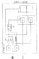
図1に本発明の原理構成を図示する。
図中、1は本発明により構成されるD−RAMカードである。
【0009】
この本発明のD−RAMカード1は、D−RAM10と、D−RAM10へのアクセスを制御するメモリ制御回路11と、カード電源として動作するバッテリ12と、本体から供給される電源か、バッテリ12から供給される電源のいずれか一方をカード電源として選択する選択手段13と、本体から供給される電源を監視することなどにより、カードが本体から離脱されているのか否かを検出する検出手段14と、D−RAM10をセルフリフレッシュモードに設定する設定手段15と、メモリ制御回路11への電源供給を切断する切断手段16とを備える。
ここで、設定手段15は、検出手段14による本体からの離脱検出時点より第1の遅延時間後に、トライステート構成の出力バッファ回路を介してD−RAMのCASラインをローレベルに設定する信号を出力する第1のゲート回路部と、検出手段14による本体からの離脱検出時点より、第1の遅延時間より長い第2の遅延時間後に、トライステート構成の出力バッファ回路を介してD−RAMのRASラインをローレベルに設定する信号を出力する第2のゲート回路部とを備えて、検出手段14が本体からの離脱を検出するときに、D−RAMをセルフリフレッシュモードに設定するという処理を行う。
【0010】
このように構成される本発明のD−RAMカード1では、選択手段13は、カードが本体に装着されるときには、本体から供給される電源をカード電源として選択し、カードが本体から離脱されるときには、バッテリ12から供給される電源をカード電源として選択する。
【0011】
このとき、設定手段15は、検出手段14によりカードが本体から離脱されていることが検出されると、D−RAM10をセルフリフレッシュモードに設定し、切断手段16は、検出手段14によりカードが本体から離脱されていることが検出されると、メモリ制御回路11への電源供給を切断する。
【0012】
このようにして、本発明によれば、カードが本体から離脱されるときには、D−RAM10を低消費電力のセルフリフレッシュモードに設定するとともに、通常のアクセス処理のときに使用するメモリ制御回路11への電源供給を切断する構成を採ることから、バッテリ12の電力消費が抑えられるようになるので、小型のD−RAMカード1を実現できるようになる。
【0013】
【発明の実施の形態】
以下、実施の形態に従って本発明を詳細に説明する。
図2に、本発明のD−RAMカード1の一実施例を図示する。
【0014】
この実施例のD−RAMカード1は、D−RAM20と、メモリ制御回路21と、セルフリフレッシュ制御回路22と、バッテリ23と、コンパレータ回路24と、第1のダイオード25と、第2のダイオード26と、スイッチ回路27とを備える。
【0015】
このメモリ制御回路21は、D−RAM20へのアクセス制御を実行するものであって、D−RAMカード1が本体と接続されているときに機能する。セルフリフレッシュ制御回路22は、コンパレータ回路24の出力信号に応答してD−RAM20をセルフリフレッシュモードに設定するものであって、D−RAMカード1が本体から離脱されているときに機能する。
【0016】
バッテリ23は、D−RAMカード1の電源として動作する。コンパレータ回路24は、本体から供給される電源の電圧レベルを基準値と比較することで、その電源が供給されているのか否かを検出して、その電源が供給されているときにはハイレベルを示し、供給されていないときにはローレベルを示すカード検出信号を出力する。
【0017】
第1のダイオード25は、本体から供給される電源を受け取る。第2のダイオード26は、バッテリ23から供給される電源を受け取る。この第1のダイオード25と第2のダイオード26の出力はワイヤードORされて、D−RAM20の電源端子に入力されるとともに、セルフリフレッシュ制御回路22/コンパレータ回路24/スイッチ回路27に供給される。
【0018】
スイッチ回路27は、第1のダイオード25と第2のダイオード26のワイヤードOR出力を入力信号として、カード検出信号がハイレベルを示すときに、その入力信号をメモリ制御回路21の電源端子に入力し、ローレベルを示すときに、その入力を遮断する。
【0019】
図3に、セルフリフレッシュ制御回路22の一実施例を図示する。
この図に示すように、セルフリフレッシュ制御回路22は、直列に接続される3つのバッファ回路30と、その後段に接続されて、制御端子にローレベルが入力されるときに入力信号をD−RAM20のRASラインに出力するトライステート構成の出力バッファ回路31とからなる第1の回路ライン40と、1つのバッファ回路32と、その後段に接続されて、制御端子にローレベルが入力されるときに入力信号をD−RAM20のCASラインに出力するトライステート構成の出力バッファ回路33とからなる第2の回路ライン41とで構成される。
【0020】
この構成に従って、セルフリフレッシュ制御回路22は、コンパレータ回路24がローレベルのカード検出信号を出力すると、図4に示すように、先ず最初に、D−RAM20のCASラインにローレベルを出力し、続いて、D−RAM20のRASラインにローレベルを出力することで、D−RAM20をセルフリフレッシュモードに設定するのである。
【0021】
なお、トライステート構成の出力バッファ回路31,33を使用するのは、メモリ制御回路21もまたD−RAM20のRASライン/CASラインを使用するから、それに影響を与えないためである。
【0022】
このように構成される本発明のD−RAMカード1では、カードが本体に装着されるときには、第1のダイオード25と第2のダイオード26のワイヤードORは、本体から供給される電源を出力し、コンパレータ回路24は、ハイレベルのカード検出信号を出力する。
【0023】
これを受けて、スイッチ回路27は、本体から供給される電源をメモリ制御回路21の電源端子に入力するので、メモリ制御回路21は、動作可能になって、本体からの指示に従ってD−RAM20をアクセスしていくとともに、D−RAM20をリフレッシュしていく。
【0024】
一方、カードが本体から離脱されるときには、第1のダイオード25と第2のダイオード26のワイヤードORは、バッテリ23から供給される電源を出力し、コンパレータ回路24は、ローレベルのカード検出信号を出力する。
【0025】
これを受けて、スイッチ回路27は、メモリ制御回路21の電源端子への電源供給を切断し、セルフリフレッシュ制御回路22は、図4で説明したように、先ず最初に、D−RAM20のCASラインにローレベルを出力し、続いて、D−RAM20のRASラインにローレベルを出力することで、D−RAM20をセルフリフレッシュモードに設定する。
【0026】
このようにして、本発明によれば、カードが本体から離脱されるときには、D−RAM20を低消費電力のセルフリフレッシュモードに設定するとともに、通常のアクセス処理のときに使用するメモリ制御回路21への電源供給を切断する構成を採ることから、バッテリ23の電力消費が抑えられるようになるので、小型のD−RAMカード1を実現できるようになる。
【0027】
図示実施例に従って本発明を説明したが、本発明はこれに限定されるものではない。例えば、実施例では、本体から供給される電源を監視することで、カードが本体から離脱されているのか否かを検出する構成を採ったが、小さなスイッチ等を使ってこれを検出するものでもよいのである。
【0028】
【発明の効果】
以上説明したように、本発明によれば、D−RAMをカードに実装することで構成されるD−RAMカードを実現できるようになる。このD−RAMカードは、S−RAMカードに比べて、メモリ容量が大きくコストも安いという大きなメリットを有している。
【図面の簡単な説明】
【図1】本発明の原理構成図である。
【図2】本発明の一実施例である。
【図3】セルフリフレッシュ制御回路の一実施例である。
【図4】セルフリフレッシュ制御回路の動作説明図である。
【符号の説明】
1 D−RAMカード
10 D−RAM
11 メモリ制御回路
12 バッテリ
13 選択手段
14 検出手段
15 設定手段
16 切断手段[0001]
BACKGROUND OF THE INVENTION
The present invention relates to a D-RAM card configured by mounting a D-RAM on a card.
[0002]
[Prior art]
Recently, an S-RAM card configured by mounting an S-RAM on a card is being used.
[0003]
This S-RAM card functions as a memory that is detachably attached to a computer device, and when removed from the computer device, retains data as it is and is used in the form of a floppy disk.
[0004]
Since the S-RAM card has low power consumption, it can be easily realized by mounting a battery as a card power source, and has recently been widely used.
[0005]
[Problems to be solved by the invention]
However, since the S-RAM has a small memory capacity and high cost, the S-RAM card has a drawback that the memory capacity is small and the cost is high.
[0006]
On the other hand, since the D-RAM has a large memory capacity and low cost, it can be considered that the D-RAM is mounted on the card instead of the S-RAM.
However, since the D-RAM consumes a large amount of power, the battery used as the card power supply becomes large, and there is a problem that the card cannot be formed as it is.
[0007]
The present invention has been made in view of such circumstances, and an object thereof is to provide a D-RAM card configured by mounting a D-RAM on a card.
[0008]
[Means for Solving the Problems]
FIG. 1 illustrates the principle configuration of the present invention.
In the figure,
[0009]
The D-
Here, the setting means 15 outputs a signal for setting the CAS line of the D-RAM to the low level via the tri-state output buffer circuit after the first delay time from the detection of the separation from the main body by the detection means 14. After a second delay time longer than the first delay time from the first gate circuit section to be output and the time point at which the detection means 14 detects the departure from the main body, the output of the D-RAM via the tri-state configuration output buffer circuit And a second gate circuit section for outputting a signal for setting the RAS line to a low level, and when the detecting means 14 detects the separation from the main body, a process of setting the D-RAM to the self-refresh mode. Do.
[0010]
In the D-
[0011]
At this time, when the detecting means 14 detects that the card is detached from the main body, the setting means 15 sets the D-RAM 10 to the self-refresh mode, and the cutting means 16 sets the card to the main body by the detecting means 14. When it is detected that the memory control circuit 11 is disconnected, the power supply to the memory control circuit 11 is cut off.
[0012]
Thus, according to the present invention, when the card is removed from the main body, the D-RAM 10 is set to the self-refresh mode with low power consumption and to the memory control circuit 11 used for normal access processing. Therefore, since the power consumption of the
[0013]
DETAILED DESCRIPTION OF THE INVENTION
Hereinafter, the present invention will be described in detail according to embodiments.
FIG. 2 shows an embodiment of the D-
[0014]
The D-
[0015]
This
[0016]
The battery 23 operates as a power source for the D-
[0017]
The first diode 25 receives power supplied from the main body. The second diode 26 receives power supplied from the battery 23. The outputs of the first diode 25 and the second diode 26 are wired-ORed and input to the power supply terminal of the D-
[0018]
The
[0019]
FIG. 3 illustrates one embodiment of the self-
As shown in this figure, the self-
[0020]
According to this configuration, when the comparator circuit 24 outputs a low level card detection signal, the self-
[0021]
The reason why the
[0022]
In the D-
[0023]
In response to this, the
[0024]
On the other hand, when the card is removed from the main body, the wired OR of the first diode 25 and the second diode 26 outputs the power supplied from the battery 23, and the comparator circuit 24 outputs a low-level card detection signal. Output.
[0025]
In response to this, the
[0026]
Thus, according to the present invention, when the card is removed from the main body, the D-
[0027]
Although the present invention has been described with reference to the illustrated embodiments, the present invention is not limited thereto. For example, in the embodiment, the power supply supplied from the main body is monitored to detect whether or not the card is detached from the main body. However, this may be detected using a small switch or the like. It's good.
[0028]
【The invention's effect】
As described above, according to the present invention, a D-RAM card configured by mounting a D-RAM on a card can be realized. This D-RAM card has a great merit that the memory capacity is large and the cost is low as compared with the S-RAM card.
[Brief description of the drawings]
FIG. 1 is a principle configuration diagram of the present invention.
FIG. 2 is an example of the present invention.
FIG. 3 is an example of a self-refresh control circuit.
FIG. 4 is an operation explanatory diagram of a self-refresh control circuit.
[Explanation of symbols]
1 D-RAM card 10 D-RAM
11
Claims (2)
バッテリと、
カードが本体に装着されるときに、本体から供給される電源をカード電源として選択し、カードが本体から離脱されるときに、上記バッテリをカード電源として選択する選択手段と、
カードが本体から離脱されているか否かを検出する検出手段と、
上記検出手段による本体からの離脱検出時点より第1の遅延時間後に、トライステート構成の出力バッファ回路を介してD−RAMのCASラインをローレベルに設定する信号を出力する第1のゲート回路部と、上記検出手段による本体からの離脱検出時点より、上記第1の遅延時間より長い第2の遅延時間後に、トライステート構成の出力バッファ回路を介してD−RAMのRASラインをローレベルに設定する信号を出力する第2のゲート回路部とを備えて、上記検出手段が本体からの離脱を検出するときに、D−RAMをセルフリフレッシュモードに設定する設定手段と、
上記検出手段が本体からの離脱を検出するときに、上記メモリ制御回路への電源供給を切断する切断手段とを備えることを、
特徴とするD−RAMカード。A D-RAM card configured by mounting a D-RAM and a memory control circuit for controlling the D-RAM on a card,
Battery,
Selecting means for selecting the power supplied from the main body as the card power when the card is mounted on the main body, and selecting the battery as the card power when the card is detached from the main body;
Detecting means for detecting whether or not the card is removed from the main body;
A first gate circuit section for outputting a signal for setting the CAS line of the D-RAM to a low level via a tri-state output buffer circuit after a first delay time from the time point when the detection means detects the separation from the main body. And the RAS line of the D-RAM is set to a low level via a tri-state output buffer circuit after a second delay time longer than the first delay time from the time point when the detection means detects the separation from the main body. and a second gate circuit for outputting a signal, when the upper Symbol detecting means detects a separation from the body, and setting means for setting the D-RAM in self-refresh mode,
A disconnecting means for disconnecting power supply to the memory control circuit when the detecting means detects separation from the main body;
Characteristic D-RAM card.
上記検出手段は、本体から供給される電源を監視することで、カードが本体から離脱されているか否かを検出することを、
特徴とするD−RAMカード。The D-RAM card according to claim 1,
The detection means detects whether the card is removed from the main body by monitoring the power supplied from the main body,
Characteristic D-RAM card.
Priority Applications (1)
| Application Number | Priority Date | Filing Date | Title |
|---|---|---|---|
| JP08232196A JP3980680B2 (en) | 1996-04-04 | 1996-04-04 | D-RAM card |
Applications Claiming Priority (1)
| Application Number | Priority Date | Filing Date | Title |
|---|---|---|---|
| JP08232196A JP3980680B2 (en) | 1996-04-04 | 1996-04-04 | D-RAM card |
Publications (2)
| Publication Number | Publication Date |
|---|---|
| JPH09274792A JPH09274792A (en) | 1997-10-21 |
| JP3980680B2 true JP3980680B2 (en) | 2007-09-26 |
Family
ID=13771309
Family Applications (1)
| Application Number | Title | Priority Date | Filing Date |
|---|---|---|---|
| JP08232196A Expired - Lifetime JP3980680B2 (en) | 1996-04-04 | 1996-04-04 | D-RAM card |
Country Status (1)
| Country | Link |
|---|---|
| JP (1) | JP3980680B2 (en) |
-
1996
- 1996-04-04 JP JP08232196A patent/JP3980680B2/en not_active Expired - Lifetime
Also Published As
| Publication number | Publication date |
|---|---|
| JPH09274792A (en) | 1997-10-21 |
Similar Documents
| Publication | Publication Date | Title |
|---|---|---|
| US5442794A (en) | Disable technique employed during low battery conditions within a portable computer system | |
| US4698582A (en) | Power driver having short circuit protection | |
| KR920005173A (en) | Semiconductor Memory with Automatic Test Mode Deviation on Chip Operation | |
| KR920005169A (en) | Semiconductor memory with flags to indicate test mode | |
| JP3980680B2 (en) | D-RAM card | |
| US8826056B2 (en) | Circuit protection system and method | |
| JPS6280716A (en) | Reset circuit for backup | |
| US5349586A (en) | Stand by control circuit | |
| JPS6230442B2 (en) | ||
| US20050049818A1 (en) | Dynamic clock pulse adjusting device | |
| JPH0756641A (en) | System for control of temperature of circuit driven by circuit clock signal | |
| US7839717B2 (en) | Semiconductor device with reduced standby failures | |
| JP4319753B2 (en) | Integrated circuit and operation control method thereof | |
| JPH06253531A (en) | Lcd bias power supply circuit | |
| JP2000137644A (en) | Memory control circuit | |
| JPH06245396A (en) | Voltage drop detector for vehicle battery power source | |
| JP2692649B2 (en) | Measuring device and logic analyzer | |
| JPH0573349A (en) | Stand-by control circuit | |
| KR20180018755A (en) | The integrated circuit inputs and outputs | |
| JPH0580913A (en) | Keyboard device | |
| CN111708290A (en) | Control system of integrated circuit and integrated circuit | |
| JP3128435B2 (en) | Computer system with resume function | |
| JPH05143788A (en) | Memory card | |
| JP2000148311A (en) | Peripheral equipment connection controller for computer | |
| JPH0450679A (en) | Semiconductor integrated circuit and apparatus for testing the same |
Legal Events
| Date | Code | Title | Description |
|---|---|---|---|
| A131 | Notification of reasons for refusal |
Free format text: JAPANESE INTERMEDIATE CODE: A131 Effective date: 20060905 |
|
| A521 | Written amendment |
Free format text: JAPANESE INTERMEDIATE CODE: A523 Effective date: 20061106 |
|
| TRDD | Decision of grant or rejection written | ||
| A01 | Written decision to grant a patent or to grant a registration (utility model) |
Free format text: JAPANESE INTERMEDIATE CODE: A01 Effective date: 20070626 |
|
| A61 | First payment of annual fees (during grant procedure) |
Free format text: JAPANESE INTERMEDIATE CODE: A61 Effective date: 20070628 |
|
| R150 | Certificate of patent or registration of utility model |
Free format text: JAPANESE INTERMEDIATE CODE: R150 |
|
| FPAY | Renewal fee payment (event date is renewal date of database) |
Free format text: PAYMENT UNTIL: 20100706 Year of fee payment: 3 |