JP3962560B2 - Substrate processing equipment - Google Patents
Substrate processing equipment Download PDFInfo
- Publication number
- JP3962560B2 JP3962560B2 JP2001201965A JP2001201965A JP3962560B2 JP 3962560 B2 JP3962560 B2 JP 3962560B2 JP 2001201965 A JP2001201965 A JP 2001201965A JP 2001201965 A JP2001201965 A JP 2001201965A JP 3962560 B2 JP3962560 B2 JP 3962560B2
- Authority
- JP
- Japan
- Prior art keywords
- substrate
- transport
- processing apparatus
- unit
- developer
- Prior art date
- Legal status (The legal status is an assumption and is not a legal conclusion. Google has not performed a legal analysis and makes no representation as to the accuracy of the status listed.)
- Expired - Fee Related
Links
Images


Description
【0001】
【発明の属する技術分野】
本発明は、液晶デバイスの製造工程において、液晶表示装置(LCD)に使用されるガラス基板上にレジストパターンを現像処理する基板処理装置に関する。
【0002】
【従来の技術】
LCDの製造工程において、LCD用のガラス基板上にITO(Indium Tin Oxide)の薄膜や電極パターンを形成するために、半導体デバイスの製造に用いられるものと同様のフォトリソグラフィ技術が利用される。フォトリソグラフィ技術では、フォトレジストをガラス基板に塗布し、これを露光し、さらに現像する。
【0003】
現像処理工程においては、パドル現像、スプレー現像等により行われており、例えばパドル現像は、現像液の表面張力を利用して基板上に現像液を盛り、この状態で基板を静止させたまま30秒〜60秒程度放置するものである。
【0004】
【発明が解決しようとする課題】
しかしながら、パドル現像では、基板上に現像液を盛ってそのままの状態で放置する方法であるので、表面張力によりガラス基板の周縁部における現像液の液膜厚が周縁部以外の領域における液膜厚よりも大きくなる。これによりレジストのレジン濃度が基板上で不均一となり、線幅が不均一となるおそれがある。
【0005】
また、バドル現像やスプレー現像において、現像液供給用のノズルから現像液を供給する際の基板に対するインパクトにより、パターン折れ、線幅の不均一性等の問題が生じている。更に当該インパクト対策のため、プリウェット(現像の前段階に、水又は希薄な現像液を基板上に数秒滴下し、レジストの表面状態を現像液になじむようにすること)は必須である。従って、このプリウェットのための装置等が必要となる。また、プリウェットにより、基板に供給された現像液は薄められるため、現像液の回収効率が悪いという問題がある。
【0006】
以上のような事情に鑑み、本発明の目的は、現像液供給の際の基板に対するインパクトを軽減し線幅の均一性を向上させることができる基板処理装置を提供することにある。
【0007】
【課題を解決するための手段】
上記目的を達成するため、本発明は、基板を所定の方向に搬送させる搬送手段と、前記搬送手段による基板の搬送方向に移動するとともに、前記搬送される基板の下面に対向して配置された多孔質部材を介して前記基板の下面全面に処理液を供給する供給手段とを具備する。
【0008】
本発明のこのような構成によれば、供給手段により処理液を吐出する場合には、多孔質部材を介して処理液がしみ出るように基板の下面全面に一様に供給することができる。しかも、処理中に供給手段を基板の搬送に合わせて移動させることにより、常に基板の下面に多孔質部材の吐出面が対向しているので、例えば、処理液が現像液の場合、現像液の表面張力により基板の周縁部で液膜厚が盛り上がることはなく、均一な液膜厚で現像処理を行うことができる。これにより、線幅均一性を向上させることができる。
【0009】
また、多孔質部材により処理液をしみ出すように基板に供給することができるので、基板に対する処理液供給のインパクトを軽減させることができ、パターン折れ等を防止することができる。
【0010】
更に、インパクトが軽減できることによりプリウェットの必要がないためプリウェットのための装置を必要とせず、また、処理液を再利用するにあたり、従来のようにプリウェットによる処理液は薄められることはないので、処理液の回収効率を向上させることができ、省エネルギー化に寄与する。
【0011】
本発明の一の形態によれば、前記多孔質部材の前記搬送される基板に対向する面は、基板の大きさとほぼ等しい。これにより、基板の下面全面に一様に処理液を供給することができる。
【0012】
本発明の一の形態によれば、前記供給手段よりも搬送下流側に設けられ、前記搬送される基板の下面及び表面にリンス液を供給して前記処理液を洗い流し及び洗浄する手段と、前記処理液が洗い流され及び洗浄された基板の下面及び表面にエアを吹きつけて乾燥させる手段とを具備する。これにより、例えば、処理液が現像液である場合、現像処理と、現像処理後に不可欠な処理であるリンス処理と、乾燥処理とを、基板を搬送させながら連続して行うことができる。
【0013】
本発明の一の形態によれば、前記搬送される基板の下面に供給するリンス液の量よりも表面に供給するリンス液の量を多くする手段と、前記搬送される基板の下面に吹き付けるエアの量よりも表面に供給するエアの量を多くする手段とを具備する。これにより、基板の下面に対してリンス処理及び乾燥処理を施す場合であっても、基板を安定に搬送させることができる。
【0014】
本発明の一の形態によれば、前記搬送手段に隣接して配置され、外部から供給される基板の表裏を反転させる機構を更に具備する。これにより、例えば、現像処理の前に基板を反転させて基板の下面側に対して現像処理を行い、次にそのままの状態でリンス処理及び乾燥処理を行うことによって、基板の下面側に付着した塵や埃等が落ちやすくなる。
【0019】
本発明の他の観点に係る基板処理装置は、基板を搬送させる搬送手段と、搬送される基板の下面に対向して配置され、該基板と対向する面が該基板の大きさとほぼ同じ大きさで、かつ、基板の搬送方向に移動自在な基板の下面全面に処理液を供給する供給手段と、前記供給手段の待機位置付近に配置され、前記基板の搬送位置を確認するためのセンサとを具備し、前記供給手段は、前記センサにより前記基板の搬送位置を確認し、前記処理液の吐出を開始するとともに、前記基板の搬送速度に合せて移動するように動作する。
本発明の一の形態によれば、前記供給手段は、前記基板の搬送速度に合せて移動している間、前記基板の下面全面に前記処理液を供給し続ける。
本発明に係る基板処理方法は、基板の表裏を反転させることにより前記基板の表面を下面側にする工程と、前記反転された基板を所定の方向に搬送しながら、基板の下面側に位置する該基板の表面全面に対して、該基板の表面とほぼ同じ大きさの処理液を供給する領域を、該基板の搬送速度に合わせて該基板の搬送方向に移動させつつ、該基板に処理液を供給する工程とを具備する。
【0020】
本発明の更なる特徴と利点は、添付した図面及び発明の実施の形態の説明を参酌することにより一層明らかになる。
【0021】
【発明の実施の形態】
以下、本発明の実施の形態を図面に基づき説明する。
【0022】
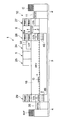
図1は本発明が適用されるLCD基板の塗布現像処理システムを示す平面図であり、図2はその正面図、また図3はその背面図である。
【0023】
この塗布現像処理システム1は、複数のガラス基板Gを収容するカセットCを載置するカセットステーション2と、基板Gにレジスト塗布および現像を含む一連の処理を施すための複数の処理ユニットを備えた処理部3と、露光装置32との間で基板Gの受け渡しを行うためのインターフェース部4とを備えており、処理部3の両端にそれぞれカセットステーション2及びインターフェース部4が配置されている。
【0024】
カセットステーション2は、カセットCと処理部3との間でLCD基板の搬送を行うための搬送機構10を備えている。そして、カセットステーション2においてカセットCの搬入出が行われる。また、搬送機構10はカセットの配列方向に沿って設けられた搬送路12上を移動可能な搬送アーム11を備え、この搬送アーム11によりカセットCと処理部3との間で基板Gの搬送が行われる。
【0025】
処理部3には、カセットステーション2におけるカセットCの配列方向(Y方向)に垂直方向(X方向)に延設された主搬送部3aと、この主搬送部3aに沿って、レジスト塗布処理ユニット(CT)を含む各処理ユニットが並設された上流部3b及び現像処理ユニット(DEV)18を含む各処理ユニットが並設された下流部3cとが設けられている。
【0026】
主搬送部3aには、X方向に延設された搬送路31と、この搬送路31に沿って移動可能に構成されガラス基板GをX方向に搬送する搬送シャトル23とが設けられている。この搬送シャトル23は、例えば支持ピンにより基板Gを保持して搬送するようになっている。また、主搬送部3aのインターフェース部4側端部には、処理部3とインターフェース部4との間で基板Gの受け渡しを行う垂直搬送ユニット7が設けられている。
【0027】
上流部3bにおいて、カセットステーション2側端部には、基板Gに洗浄処理を施すスクラバ洗浄処理ユニット(SCR)20が設けられ、このスクラバ洗浄処理ユニット(SCR)20の上段に基板G上の有機物を除去するためのエキシマUV処理ユニット(e−UV)19が配設されている。
【0028】
スクラバ洗浄処理ユニット(SCR)20には、ローラ型の搬送装置50が設けられており、この搬送装置50により基板Gは水平に搬送されながら洗浄処理されるようになっている。また、このスクラバ洗浄処理ユニット(SCR)20の両端には、外部と間で基板の受け渡しを行うための上下昇降機構を有する受け渡しピン46が設けられている。
【0029】
スクラバ洗浄処理ユニット(SCR)20の隣には、ガラス基板Gに対して熱的処理を行うユニットが多段に積み上げられた熱処理系ブロック24及び25が配置されている。これら熱処理系ブロック24と25との間には、垂直搬送ユニット5が配置され、搬送アーム5aがZ方向及び水平方向に移動可能とされ、かつθ方向に回動可能とされているので、両ブロック24及び25における各熱処理系ユニットにアクセスして基板Gの搬送が行われるようになっている。なお、上記処理部3における垂直搬送ユニット7についてもこの垂直搬送ユニット5と同一の構成を有している。
【0030】
図2に示すように、熱処理系ブロック24には、基板Gにレジスト塗布前の加熱処理を施すベーキングユニット(BEKE)が2段、HMDSガスにより疎水化処理を施すアドヒージョンユニット(AD)が下から順に積層されている。一方、熱処理系ブロック25には、基板Gに冷却処理を施すクーリングユニット(COL)が2段、アドヒージョンユニット(AD)が下から順に積層されている。
【0031】
熱処理系ブロック25に隣接してレジスト処理ブロック15がX方向に延設されている。このレジスト処理ブロック15は、基板Gにレジストを塗布するレジスト塗布処理ユニット(CT)と、減圧により前記塗布されたレジストを乾燥させる減圧乾燥ユニット(VD)と、基板Gの周縁部のレジストを除去するエッジリムーバ(ER)とが一体的に設けられて構成されている。このレジスト処理ブロック15には、レジスト塗布処理ユニット(CT)からエッジリムーバ(ER)にかけて移動する図示しないサブアームが設けられており、このサブアームによりレジスト処理ブロック15内で基板Gが搬送されるようになっている。
【0032】
レジスト処理ブロック15に隣接して多段構成の熱処理系ブロック26が配設されており、この熱処理系ブロック26には、基板Gにレジスト塗布後の加熱処理を行うプリベーキングユニット(PREBAKE)が3段積層されている。
【0033】
下流部3cにおいては、図3に示すように、インターフェース部4側端部には、熱処理系ブロック29が設けられており、これには、クーリングユニット(COL)、露光後現像処理前の加熱処理を行うポストエクスポージャーベーキングユニット(PEBAKE)が2段、下から順に積層されている。
【0034】
熱処理系ブロック29に隣接して、本発明に係る現像処理ユニット(DEV)18がX方向に延設されている。この現像処理ユニット(DEV)については後述する。この現像処理ユニット(DEV)18の隣には熱処理系ブロック28及び27が配置され、これら熱処理系ブロック28と27との間には、上記垂直搬送ユニット5と同一の構成を有し、両ブロック28及び27における各熱処理系ユニットにアクセス可能な垂直搬送ユニット6が設けられている。また、現像処理ユニット(DEV)18端部の上には、i線処理ユニット(i―UV)33が設けられている。
【0035】
熱処理系ブロック28には、クーリングユニット(COL)、基板Gに現像後の加熱処理を行うポストベーキングユニット(POBAKE)が2段、下から順に積層されている。一方、熱処理系ブロック27も同様に、クーリングユニット(COL)、ポストベーキングユニット(POBAKE)が2段、下から順に積層されている。
【0036】
インターフェース部4には、正面側にタイトラー及び周辺露光ユニット(Titler/EE)22が設けられ、垂直搬送ユニット7に隣接してエクステンションクーリングユニット(EXTCOL)35が、また背面側にはバッファカセット34が配置されており、これらタイトラー及び周辺露光ユニット(Titler/EE)22とエクステンションクーリングユニット(EXTCOL)35とバッファカセット34と隣接した露光装置32との間で基板Gの受け渡しを行う垂直搬送ユニット8が配置されている。この垂直搬送ユニット8も上記垂直搬送ユニット5と同一の構成を有している。
【0037】
図4は、本発明の第1の実施形態に係る現像処理ユニット(DEV)の側面図である。この現像処理ユニット(DEV)には、基板GをX方向に搬送する手段として、図示しないモータにより回転駆動される複数の搬送ローラ41が設けられている。この搬送ローラ41による搬送上流側(図中左)には、基板Gの下面側に配置され現像液を供給する現像液ノズル43が設けられている。この現像液ノズル43の下流側においては、基板Gに対しそれぞれリンス液を供給して、現像液を洗い流し及び洗浄する第1リンスノズル77及び第2リンスノズル76が基板Gの下面及び上面に配置されている。この第1リンスノズル77及び第2リンスノズル76の下流側においては、基板Gにエアを吹き付けて乾燥させる第1エア供給装置79及び第2エア供給装置78が基板Gの下面及び上面に配置されている。
【0038】
上記第2リンスノズル76のリンス液の供給量を第1リンスノズル77のリンス液の供給量よりも多くなるようにされている。また、第2エア供給装置78のエアの供給量を第1エア供給装置79のエアの供給量よりも多くなるようにされている。これにより、基板Gの下面に対してリンス処理及び乾燥処理を施す場合であっても、基板Gを安定に搬送させることができる。
【0039】
図5及び図6は、現像処理ユニット(DEV)における上記現像液ノズル43が配置された部位の正面図及び平面図である。例えば、上記搬送ローラ41にはフランジ部41aが形成されており、基板Gはこのフランジ部41aに載置され搬送されるようになっている。現像液ノズル43は、例えば垂直の支持体44により、搬送される基板Gに対してわずかな隙間を空けて支持されている。また、現像液ノズル43の基板Gに対向する面は基板Gの大きさとほぼ同じ大きさとされている。支持体44は台部45に固定されており、この台部45には、例えば基板Gの搬送方向に延設されたレール49に沿って走行する車輪47が設けられ、駆動モータ42により基板Gの搬送方向に移動可能とされている。
【0040】
図7は、現像液ノズル43の断面図である。この現像液ノズル43は、現像液を貯留するためのバッファ室59を有するマニホールド48に、複数の孔52aが形成された多孔質部材52が接続されている。マニホールド48には、例えば図示しない供給源からの現像液を供給するための供給口48aが複数形成されている。上述したように、この現像液ノズル43は、搬送される基板Gの下面側に隙間を空けて配置されている。
【0041】
図8は、一実施形態に係る反転機構を示す斜視図である。この反転機構は、例えば、基板Gを真空吸着するための吸着部56を複数有するコ字形状部材75が、支持部材58の軸54に回動可能に軸支されている。この反転機構は、例えば現像処理ユニット(DEV)における搬送上流端及び搬送下流端に配置されている。
【0042】
図9に示すように、この反転機構は、垂直搬送ユニット7の搬送アームから基板Gが受け渡された後反転し、図10に示す状態となる。そしてこの状態から現像処理ユニット(DEV)の受け渡しピン46が上昇して、基板Gが受け渡しピン46に受け渡されるようになっている。
【0043】
以上のように構成された塗布現像処理システム1の処理工程については、先ずカセットC内の基板Gが処理部3における上流部3bに搬送される。上流部3bでは、エキシマUV処理ユニット(e−UV)19において表面改質・有機物除去処理が行われ、次にスクラバ洗浄処理ユニット(SCR)20において、搬送装置50により基板Gが略水平に搬送されながら洗浄処理及び乾燥処理が行われる。続いて熱処理系ブロック24の最下段部で垂直搬送ユニットにおける搬送アーム5aにより基板Gが取り出され、同熱処理系ブロック24のベーキングユニット(BEKE)にて加熱処理、アドヒージョンユニット(AD)にて疎水化処理が行われ、熱処理系ブロック25のクーリングユニット(COL)による冷却処理が行われる。
【0044】
次に、基板Gは搬送アーム5aから搬送シャトル23に受け渡される。そしてレジスト塗布処理ユニット(CT)に搬送され、レジストの塗布処理が行われた後、減圧乾燥処理ユニット(VD)にて減圧乾燥処理、エッジリムーバ(ER)にて基板周縁のレジスト除去処理が順次行われる。
【0045】
次に、基板Gは搬送シャトル23から垂直搬送ユニット7の搬送アームに受け渡され、熱処理系ブロック26におけるプリベーキングユニット(PREBAKE)にて加熱処理が行われた後、熱処理系ブロック29におけるクーリングユニット(COL)にて冷却処理が行われる。続いて基板Gはエクステンションクーリングユニット(EXTCOL)35にて冷却処理されるとともに露光装置にて露光処理される。
【0046】
次に、基板Gは垂直搬送ユニット8及び7の搬送アームを介して熱処理系ブロック29のポストエクスポージャーベーキングユニット(PEBAKE)に搬送され、ここで加熱処理が行われた後、クーリングユニット(COL)にて冷却処理が行われる。そして基板Gは、熱処理系ブロック29の最下段において垂直搬送ユニット7の搬送アームから反転機構に受け渡される。
【0047】
そして反転機構により反転された基板Gは、図11(a)に示すように、受け渡しピン46に受け渡されて下降する。基板Gが搬送上流端の搬送ローラ41に載置されると、同図(b)に示すように搬送され、現像液ノズル43上に搬送されてくる。ここで、例えば現像液ノズルの待機位置付近に配置された光学センサSにより基板Gの搬送位置を確認してから、現像液ノズル43は現像液の吐出を開始するとともに、同図(c)に示すように、基板Gの搬送速度に合わせて移動を開始する。この現像液ノズル43の移動中は、現像液を吐出し続けるようにし、現像処理を行う。この後、搬送下流側で基板Gはリンス処理が及び乾燥処理が行われる。
【0048】
現像液ノズル43により現像液を吐出する場合には、多孔質部材52を介して現像液55がしみ出るように基板Gの下面全面に一様に供給することができる。しかも、現像処理中に現像液ノズル43を基板Gの搬送に合わせて移動させることにより、常に基板Gの下面に多孔質部材52の吐出面が対向しているので、従来のような液盛り現像中において、現像液の表面張力により基板Gの周縁部で液膜厚が盛り上がることはなく、均一な液膜厚で現像処理を行うことができる。これにより、線幅均一性を向上させることができる。
【0049】
また、多孔質部材52により現像液をしみ出すように基板Gに供給しているので、基板Gに対する現像液のインパクトを軽減させることができ、パターン折れ等を防止することができる。
【0050】
また、本実施形態では、インパクトが軽減できることによりプリウェットの必要がないため、プリウェットのための装置を必要とせず、また、現像液を再利用するにあたり、従来のようにプリウェットによる現像液は薄められることはないので、現像液の回収効率を向上させることができる。
【0051】
更に、本実施形態によれば、現像処理の前に基板Gを反転させて基板の下面側に対して現像処理を行い、次にそのままの状態でリンス処理及び乾燥処理を行うこととしたので、このリンス処理及び乾燥処理によって基板の下面側に付着した塵や埃等が落ちやすいという作用効果を奏する。
【0052】
現像処理ユニット(DEV)による現像処理が終了すると、基板Gは熱処理系ブロック28における最下段において反転機構により反転され、垂直搬送ユニット6の搬送アーム6aにより受け渡される。そして熱処理系ブロック28又は27におけるポストベーキングユニット(POBAKE)で加熱処理が行われ、クーリングユニット(COL)にて冷却処理が行われる。そして基板Gは搬送機構10に受け渡されカセットCに収容される。
【0053】
図12及び図13は、本発明の第2の実施形態に係る現像処理ユニット(DEV)の一部を示す斜視図及び側面図である。
【0054】
本実施形態では、基板Gの面と平行に回転する複数の搬送ローラ61により基板Gが水平方向に搬送されるようになっている。この搬送ローラ61は基板の両端を挟むような形状に形成されており、回転により基板Gを搬送する。搬送される基板Gの下面には、長尺状の現像液ノズル65が基板Gの搬送方向に複数配列されている。この現像液ノズル65は、上記第1の実施形態と同様の構成を有しており、供給管64から供給される現像液を、バッファ室を有するマニホールド及び多孔質部材63を介して基板の下面側にしみ出るように供給するようになっている。
【0055】
本実施形態によっても、上記第1の実施形態と同様の効果が得られる。本実施形態では、搬送される基板Gに対応して基板Gに対向するノズルのみにより現像液を吐出させるようにし、基板Gに対向しない他のノズルは吐出を停止することが好ましいが、全てのノズルにより現像液を常に吐出さておくようにすることももちろん可能である。
【0056】
以上、上記各実施形態において、ガラス基板をローラ搬送等により水平に搬送させながら現像処理を行う場合について説明したが、これらに限定されるものではない。例えば、図14及び図15に示すように、カップCP内に配置された保持部66により基板Gを吸着保持して現像を行う現像処理ユニットにも本発明は適用可能である。
【0057】
本実施形態の現像液ノズルは、上記第1の実施形態と同一の現像液ノズル43を使用しており、この現像液ノズル43は、昇降支持部材72により支持され、駆動部80によって昇降可能に配置されている。この駆動部80は現像液ノズル43と基板Gとの距離を例えば数mm単位又はこれ以下の単位で制御するようになっている。
【0058】
なお、この現像処理ユニット以外の外部とこの現像処理ユニットとの間で基板Gが搬送される際は、現像液ノズル43は上昇している状態で待機している状態となっている。また、保持部66は、基板Gの受け渡しのためにモータ部74により昇降可能となっており、更に液切り乾燥処理のために回転可能とされている。なお、本実施形態では図示を省略したが、リンス液を供給するリンスノズルももちろん設けられている。
【0059】
本実施形態の現像処理ユニットにおいて基板Gに現像液を供給する場合には、先ず現像液ノズル43を基板Gに対して近づけ、この近づけた状態から現像液68の吐出を開始し、徐々に現像液ノズル43を基板Gから離していく。そして図16に示すように、基板Gと現像液ノズル43との距離が所定の距離に達したら現像液の吐出を停止し、ノズル43を当該所定の距離を保った位置で現像処理が終了するまで保持しておく。
【0060】
従って、従来の液盛り現像では、図17に示すように現像液85が基板Gの周縁部で盛り上がってしまい均一な液盛り状態での現像処理ができなかったが、本実施形態によれば、基板全面における液膜厚を所定の値で均一に保つことができる。また、本実施形態では現像液ノズル43による張力が現像液68に加わるため、現像液の量を従来より多い状態で現像処理を行うことができる。現像液の量が少ない場合、現像液にレジスト材料が溶け出して副生成物ができ、これにより反応速度が変化する傾向があるが、本実施形態では現像液の量が多いので処理能力が安定する。
【0061】
更に本実施形態によれば、従来型の静止現像を行う現像処理ユニット及びこの現像処理ユニットを含むレジスト塗布現像処理システムにも応用できる。
【0062】
なお、現像液ノズルの基板Gに対する距離を制御して液膜厚を制御する方法は、上記第1の実施形態及び第2の実施形態においても適用可能である。例えば、図5に示す支持体44を伸縮自在に構成して、基板Gと現像液ノズル43との距離を制御可能にしてもよい。また、図12及び図13に示す各現像液ノズル65についても同様である。
【0063】
【発明の効果】
以上説明したように、本発明によれば、現像液供給の際の基板に対するインパクトを軽減し線幅の均一性を向上させることができる。
【図面の簡単な説明】
【図1】本発明が適用される塗布現像処理システムの全体構成を示す平面図である。
【図2】図1に示す塗布現像処理システムの正面図である。
【図3】図1に示す塗布現像処理システムの背面図である。
【図4】本発明の一実施形態に係る現像処理ユニット(DEV)の側面図である。
【図5】図4に示す現像処理ユニット(DEV)における現像液ノズルの正面図である。
【図6】同現像液ノズルの平面図である。
【図7】同現像液ノズルの断面図である。
【図8】本発明の一実施形態に係る反転機構を示す斜視図である。
【図9】図8に示す反転機構の側面図である。
【図10】図8に示す反転機構の反転した状態を示す側面図である。
【図11】受け渡しピンから現像液ノズルまで搬送される際の作用図である。
【図12】本発明の第2の実施形態に係る現像処理ユニットの一部を示す斜視図である。
【図13】図12に示す現像処理ユニットにおける現像液ノズルの側面図である。
【図14】本発明の他の実施形態に係る現像処理ユニットの一部を示す平面図である。
【図15】図14に示す現像処理ユニットの一部の断面図である。
【図16】現像液ノズルによる液盛り状態を示す側面図である。
【図17】従来の液盛り状態を示す側面図である。
【符号の説明】
G…ガラス基板
41…搬送ローラ
41a…フランジ部
42…駆動モータ
43、65…現像液ノズル
48…マニホールド
48a…供給口
49…レール
52a…孔
52、63…多孔質部材
54…軸
55、68…現像液
56…吸着部
58…支持部材
59…バッファ室
61…搬送ローラ
66…保持部
72…昇降支持部材
74…モータ部
75…コ字形状部材
76、77…リンスノズル
78、79…エア供給装置
80…駆動部[0001]
BACKGROUND OF THE INVENTION
The present invention relates to a substrate processing apparatus for developing a resist pattern on a glass substrate used in a liquid crystal display device (LCD) in a manufacturing process of a liquid crystal device.
[0002]
[Prior art]
In the LCD manufacturing process, a photolithography technique similar to that used for manufacturing semiconductor devices is used to form an ITO (Indium Tin Oxide) thin film or electrode pattern on a glass substrate for LCD. In the photolithography technique, a photoresist is applied to a glass substrate, which is exposed and further developed.
[0003]
In the development processing step, paddle development, spray development, or the like is performed. For example, paddle development is performed by depositing the developer on the substrate using the surface tension of the developer, and keeping the substrate stationary in this state. It is left for about 60 seconds.
[0004]
[Problems to be solved by the invention]
However, since paddle development is a method in which the developer is deposited on the substrate and left as it is, the liquid film thickness of the developer at the peripheral portion of the glass substrate due to surface tension is the liquid film thickness in the region other than the peripheral portion. Bigger than. As a result, the resin concentration of the resist becomes nonuniform on the substrate, and the line width may become nonuniform.
[0005]
Further, in the paddle development and spray development, problems such as pattern breakage and non-uniformity of the line width occur due to the impact on the substrate when the developer is supplied from the developer supply nozzle. Furthermore, pre-wet (in the pre-development stage, water or a dilute developer is dropped on the substrate for several seconds so that the resist surface state is adjusted to the developer) is indispensable as a countermeasure against the impact. Therefore, an apparatus for this pre-wet is required. Further, since the developer supplied to the substrate is diluted by pre-wetting, there is a problem that the recovery efficiency of the developer is poor.
[0006]
In view of the circumstances as described above, an object of the present invention is to provide a substrate processing apparatus capable of reducing the impact on a substrate when supplying a developing solution and improving the uniformity of the line width.
[0007]
[Means for Solving the Problems]
In order to achieve the above object, the present invention is arranged to convey a substrate in a predetermined direction, and to move in the substrate conveyance direction by the conveyance unit, and to face the lower surface of the substrate to be conveyed. Supply means for supplying a processing liquid to the entire lower surface of the substrate through a porous member.
[0008]
According to such a configuration of the present invention, when the processing liquid is discharged by the supply unit, the processing liquid can be uniformly supplied to the entire lower surface of the substrate so as to ooze out through the porous member. Moreover, since the discharge surface of the porous member always faces the lower surface of the substrate by moving the supply unit in accordance with the conveyance of the substrate during processing, for example, when the processing solution is a developing solution, The liquid film thickness does not rise at the peripheral edge of the substrate due to the surface tension, and the development processing can be performed with a uniform liquid film thickness. Thereby, line width uniformity can be improved.
[0009]
In addition, since the processing liquid can be supplied to the substrate so as to ooze out by the porous member, the impact of the processing liquid supply to the substrate can be reduced, and pattern breakage and the like can be prevented.
[0010]
Furthermore, since the impact can be reduced, pre-wetting is not required, so no pre-wetting device is required, and when the processing liquid is reused, the pre-wetting processing liquid is not diluted as in the prior art. Therefore, the recovery efficiency of the treatment liquid can be improved, which contributes to energy saving.
[0011]
According to one aspect of the present invention, the surface of the porous member that faces the transported substrate is substantially equal to the size of the substrate. Thereby, the processing liquid can be uniformly supplied to the entire lower surface of the substrate.
[0012]
According to one aspect of the present invention, the means provided on the downstream side of the supply relative to the supply means, supplies a rinsing liquid to the lower surface and the surface of the substrate to be transferred, and rinses and cleans the processing liquid; And a means for spraying air to the lower surface and the surface of the cleaned substrate, and drying the substrate. Thereby, for example, when the processing solution is a developing solution, the developing process, the rinsing process that is an indispensable process after the developing process, and the drying process can be continuously performed while the substrate is conveyed.
[0013]
According to one aspect of the present invention, the means for increasing the amount of the rinsing liquid supplied to the surface than the amount of the rinsing liquid supplied to the lower surface of the substrate to be transported, and the air blown to the lower surface of the substrate to be transported Means for increasing the amount of air supplied to the surface rather than the amount of. Thereby, even if it is a case where the rinse process and a drying process are performed with respect to the lower surface of a board | substrate, a board | substrate can be conveyed stably.
[0014]
According to an aspect of the present invention, the apparatus further includes a mechanism that is disposed adjacent to the transport unit and reverses the front and back of the substrate supplied from the outside. Thus, for example, the substrate is inverted before the developing process, the developing process is performed on the lower surface side of the substrate, and then the substrate is attached to the lower surface side of the substrate by performing a rinsing process and a drying process in the same state. Dust and dust easily fall off.
[0019]
A substrate processing apparatus according to another aspect of the present invention is arranged so as to face a lower surface of a substrate to be transferred, a transfer means for transferring a substrate, and a surface facing the substrate is substantially the same size as the size of the substrate. And a supply means for supplying the processing liquid to the entire lower surface of the substrate movable in the substrate transfer direction, and a sensor arranged near the standby position of the supply means for confirming the transfer position of the substrate. The supply means checks the transport position of the substrate by the sensor, starts to discharge the processing liquid, and operates to move according to the transport speed of the substrate.
According to an aspect of the present invention, the supply unit continues to supply the processing liquid to the entire lower surface of the substrate while moving in accordance with the transfer speed of the substrate .
In the substrate processing method according to the present invention, the surface of the substrate is turned to the lower surface side by reversing the front and back of the substrate, and the substrate is positioned on the lower surface side of the substrate while transporting the reversed substrate in a predetermined direction. A region for supplying a processing liquid having the same size as the surface of the substrate to the entire surface of the substrate is moved in the substrate transport direction in accordance with the substrate transport speed, while the processing liquid is applied to the substrate. A step of supplying
[0020]
Further features and advantages of the present invention will become more apparent by referring to the attached drawings and description of embodiments of the invention.
[0021]
DETAILED DESCRIPTION OF THE INVENTION
Hereinafter, embodiments of the present invention will be described with reference to the drawings.
[0022]
FIG. 1 is a plan view showing an LCD substrate coating and developing system to which the present invention is applied, FIG. 2 is a front view thereof, and FIG. 3 is a rear view thereof.
[0023]
The coating and developing processing system 1 includes a
[0024]
The
[0025]
The
[0026]
The
[0027]
In the
[0028]
The scrubber cleaning processing unit (SCR) 20 is provided with a roller-
[0029]
Next to the scrubber cleaning processing unit (SCR) 20, thermal processing blocks 24 and 25 are arranged in which units for performing thermal processing on the glass substrate G are stacked in multiple stages. Between these heat treatment blocks 24 and 25, the
[0030]
As shown in FIG. 2, the heat
[0031]
A resist
[0032]
A multi-stage heat
[0033]
In the
[0034]
A development processing unit (DEV) 18 according to the present invention extends in the X direction adjacent to the
[0035]
In the
[0036]
The
[0037]
FIG. 4 is a side view of the development processing unit (DEV) according to the first embodiment of the present invention. The development processing unit (DEV) is provided with a plurality of
[0038]
The amount of the rinse liquid supplied from the second rinse
[0039]
5 and 6 are a front view and a plan view of a portion where the
[0040]
FIG. 7 is a cross-sectional view of the
[0041]
FIG. 8 is a perspective view showing a reversing mechanism according to an embodiment. In this reversing mechanism, for example, a
[0042]
As shown in FIG. 9, the reversing mechanism is reversed after the substrate G is transferred from the transport arm of the vertical transport unit 7, and the state shown in FIG. From this state, the
[0043]
The configured coating and developing treatment system 1 of the processing steps as described above, first, the substrate G in the cassette C is transported to the
[0044]
Next, the substrate G is transferred from the
[0045]
Next, the substrate G is transferred from the
[0046]
Next, the substrate G is transferred to the post-exposure baking unit (PEBAKE) of the heat
[0047]
Then, the substrate G reversed by the reversing mechanism is delivered to the delivery pins 46 and lowered as shown in FIG. When the substrate G is placed on the
[0048]
When the developer is discharged from the
[0049]
Further, since the supply to the substrate G to ooze the current image was more
[0050]
Further, in this embodiment, since the impact can be reduced, pre-wetting is not necessary, so no pre-wetting device is required, and when the developer is reused, the pre-wet developer as in the past is used. Since it is not diluted, the recovery efficiency of the developer can be improved.
[0051]
Furthermore, according to the present embodiment, the substrate G is inverted before the development processing, the development processing is performed on the lower surface side of the substrate, and then the rinsing processing and the drying processing are performed as they are. The rinsing process and the drying process have an effect that dust and dirt attached to the lower surface side of the substrate easily fall off.
[0052]
When the development processing by the development processing unit (DEV) is completed, the substrate G is reversed by the reversing mechanism at the lowest stage in the heat
[0053]
12 and 13 are a perspective view and a side view showing a part of a development processing unit (DEV) according to the second embodiment of the present invention.
[0054]
In the present embodiment, the substrate G is transported in the horizontal direction by a plurality of
[0055]
Also according to this embodiment, the same effect as the first embodiment can be obtained. In this embodiment, it is preferable that the developer is discharged only by the nozzle facing the substrate G corresponding to the substrate G to be transported, and the other nozzles not facing the substrate G are preferably stopped from discharging. Of course, it is possible to always discharge the developer by the nozzle.
[0056]
As described above, in each of the above embodiments, the case where the development processing is performed while the glass substrate is transported horizontally by roller transportation or the like has been described, but the present invention is not limited thereto. For example, as shown in FIGS. 14 and 15, the present invention is also applicable to a development processing unit that performs development by sucking and holding the substrate G by the holding
[0057]
The developer nozzle of this embodiment uses the
[0058]
Note that when the substrate G is transported between the outside of the development processing unit and the development processing unit, the developing
[0059]
When the developing unit in the present embodiment to supply the developing solution to the substrate G, first close the
[0060]
Therefore, in the conventional liquid pile development, as shown in FIG. 17, the
[0061]
Furthermore, according to this embodiment, the present invention can be applied to a conventional development processing unit for performing static development and a resist coating and development processing system including this development processing unit.
[0062]
The method of controlling the film thickness by controlling the distance of the developer nozzle to the substrate G can also be applied to the first embodiment and the second embodiment. For example, the
[0063]
【The invention's effect】
As described above, according to the present invention, it is possible to reduce the impact on the substrate when supplying the developer and improve the uniformity of the line width.
[Brief description of the drawings]
FIG. 1 is a plan view showing an overall configuration of a coating and developing treatment system to which the present invention is applied.
FIG. 2 is a front view of the coating and developing treatment system shown in FIG.
FIG. 3 is a rear view of the coating and developing treatment system shown in FIG. 1;
FIG. 4 is a side view of a development processing unit (DEV) according to an embodiment of the present invention.
5 is a front view of a developer nozzle in the development processing unit (DEV) shown in FIG. 4. FIG.
FIG. 6 is a plan view of the developer nozzle.
FIG. 7 is a cross-sectional view of the developer nozzle.
FIG. 8 is a perspective view showing a reversing mechanism according to an embodiment of the present invention.
9 is a side view of the reversing mechanism shown in FIG.
10 is a side view showing a reversed state of the reversing mechanism shown in FIG. 8. FIG.
FIG. 11 is an operation diagram when transported from a delivery pin to a developer nozzle.
FIG. 12 is a perspective view showing a part of a development processing unit according to a second embodiment of the present invention.
13 is a side view of a developer nozzle in the development processing unit shown in FIG.
FIG. 14 is a plan view showing a part of a development processing unit according to another embodiment of the present invention.
15 is a cross-sectional view of a part of the development processing unit shown in FIG.
FIG. 16 is a side view showing a state of liquid accumulation by a developer nozzle.
FIG. 17 is a side view showing a conventional liquid accumulation state.
[Explanation of symbols]
G ...
Claims (8)
前記搬送手段による基板の搬送方向に移動するとともに、前記搬送される基板の下面に対向して配置された多孔質部材を介して前記基板の下面全面に処理液を供給する供給手段と
を具備することを特徴とする基板処理装置。Transport means for transporting the substrate in a predetermined direction;
And a supply unit that moves in the substrate transport direction by the transport unit and that supplies a processing liquid to the entire lower surface of the substrate through a porous member disposed to face the lower surface of the transported substrate. A substrate processing apparatus.
前記多孔質部材の前記搬送される基板に対向する面は、基板の大きさとほぼ等しいことを特徴とする基板処理装置。The substrate processing apparatus according to claim 1,
The substrate processing apparatus, wherein a surface of the porous member facing the substrate to be conveyed is substantially equal to the size of the substrate.
前記供給手段よりも搬送下流側に設けられ、前記搬送される基板の下面及び表面にリンス液を供給して前記処理液を洗い流し及び洗浄する手段と、
前記処理液が洗い流され及び洗浄された基板の下面及び表面にエアを吹きつけて乾燥させる手段と
を具備することを特徴とする基板処理装置。In the substrate processing apparatus of Claim 1 or Claim 2,
Means for providing a rinsing liquid to the lower surface and the surface of the substrate to be transported to wash away and wash the processing liquid, which is provided on the downstream side of transport relative to the supply means;
A substrate processing apparatus comprising: means for blowing air to the lower surface and the surface of the cleaned substrate, and drying the substrate.
前記搬送される基板の下面に供給するリンス液の量よりも表面に供給するリンス液の量を多くする手段と、
前記搬送される基板の下面に吹き付けるエアの量よりも表面に供給するエアの量を多くする手段と
を具備することを特徴とする基板処理装置。In the substrate processing apparatus of any one of Claims 1-3,
Means for increasing the amount of rinsing liquid supplied to the surface rather than the amount of rinsing liquid supplied to the lower surface of the substrate to be transported;
And a means for increasing the amount of air supplied to the surface rather than the amount of air blown onto the lower surface of the substrate to be transported.
前記搬送手段に隣接して配置され、外部から供給される基板の表裏を反転させる機構を更に具備することを特徴とする基板処理装置。In the substrate processing apparatus of any one of Claims 1-4,
A substrate processing apparatus, further comprising a mechanism that is disposed adjacent to the transfer means and reverses the front and back of a substrate supplied from the outside.
搬送される基板の下面に対向して配置され、該基板と対向する面が該基板の大きさとほぼ同じ大きさで、かつ、基板の搬送方向に移動自在な基板の下面全面に処理液を供給する供給手段と、
前記供給手段の待機位置付近に配置され、前記基板の搬送位置を確認するためのセンサと
を具備し、
前記供給手段は、前記センサにより前記基板の搬送位置を確認し、前記処理液の吐出を開始するとともに、前記基板の搬送速度に合せて移動するように動作することを特徴とする基板処理装置。Transport means for transporting the substrate;
The processing liquid is arranged across the lower surface of the substrate to be transported, the surface facing the substrate is approximately the same size as the substrate, and the processing liquid is supplied to the entire lower surface of the substrate movable in the substrate transport direction. Supply means for
A sensor disposed near a standby position of the supply means, and for confirming a transfer position of the substrate;
The substrate processing apparatus is characterized in that the supply means confirms the transport position of the substrate by the sensor, starts discharging the processing liquid, and operates to move according to the transport speed of the substrate.
前記供給手段は、前記基板の搬送速度に合せて移動している間、前記基板の下面全面に前記処理液を供給し続けることを特徴とする基板処理装置。The substrate processing apparatus according to claim 6 ,
The substrate processing apparatus, wherein the supply means continues to supply the processing liquid to the entire lower surface of the substrate while moving in accordance with the transport speed of the substrate.
前記反転された基板を所定の方向に搬送しながら、基板の下面側に位置する該基板の表面全面に対して、該基板の表面とほぼ同じ大きさの処理液を供給する領域を、該基板の搬送速度に合わせて該基板の搬送方向に移動させつつ、該基板に処理液を供給する工程と
を具備することを特徴とする基板処理方法。Reversing the front and back of the substrate to make the surface of the substrate the lower surface,
An area for supplying a processing liquid having the same size as the surface of the substrate to the entire surface of the substrate located on the lower surface side of the substrate while transporting the inverted substrate in a predetermined direction. And a step of supplying a processing liquid to the substrate while moving the substrate in the transport direction in accordance with the transport speed of the substrate.
Priority Applications (1)
| Application Number | Priority Date | Filing Date | Title |
|---|---|---|---|
| JP2001201965A JP3962560B2 (en) | 2001-07-03 | 2001-07-03 | Substrate processing equipment |
Applications Claiming Priority (1)
| Application Number | Priority Date | Filing Date | Title |
|---|---|---|---|
| JP2001201965A JP3962560B2 (en) | 2001-07-03 | 2001-07-03 | Substrate processing equipment |
Publications (3)
| Publication Number | Publication Date |
|---|---|
| JP2003017392A JP2003017392A (en) | 2003-01-17 |
| JP2003017392A5 JP2003017392A5 (en) | 2004-10-14 |
| JP3962560B2 true JP3962560B2 (en) | 2007-08-22 |
Family
ID=19038852
Family Applications (1)
| Application Number | Title | Priority Date | Filing Date |
|---|---|---|---|
| JP2001201965A Expired - Fee Related JP3962560B2 (en) | 2001-07-03 | 2001-07-03 | Substrate processing equipment |
Country Status (1)
| Country | Link |
|---|---|
| JP (1) | JP3962560B2 (en) |
Families Citing this family (1)
| Publication number | Priority date | Publication date | Assignee | Title |
|---|---|---|---|---|
| JP4886719B2 (en) * | 2008-03-14 | 2012-02-29 | 日立ビアメカニクス株式会社 | Processing equipment |
-
2001
- 2001-07-03 JP JP2001201965A patent/JP3962560B2/en not_active Expired - Fee Related
Also Published As
| Publication number | Publication date |
|---|---|
| JP2003017392A (en) | 2003-01-17 |
Similar Documents
| Publication | Publication Date | Title |
|---|---|---|
| JP4040025B2 (en) | Coating film forming device | |
| JP4554397B2 (en) | Stage device and coating treatment device | |
| JP4678658B2 (en) | Coating device | |
| JP3868223B2 (en) | Transport device | |
| TWI311633B (en) | Decompression drier | |
| JP3887549B2 (en) | Substrate transfer device | |
| JP3741655B2 (en) | Liquid processing method and liquid processing apparatus | |
| JP2003051529A (en) | Conveyer | |
| JP4022288B2 (en) | Substrate processing equipment | |
| JP4982306B2 (en) | Coating apparatus and coating method | |
| JP2002110506A (en) | Application device and method therefor | |
| JP3704064B2 (en) | Liquid processing apparatus and liquid processing method | |
| JP3754905B2 (en) | Substrate dryer | |
| JP4450825B2 (en) | Substrate processing method, resist surface processing apparatus, and substrate processing apparatus | |
| JP3930278B2 (en) | Liquid processing apparatus and liquid processing method | |
| KR101568050B1 (en) | Substrate processing apparatus | |
| JP4353530B2 (en) | Substrate processing method and substrate processing apparatus | |
| JP2002334918A (en) | Treating apparatus | |
| KR20110066864A (en) | Substrate processing apparatus, substrate processing method and recording medium storing program for executing the substrate processing method | |
| JP3962560B2 (en) | Substrate processing equipment | |
| JP3605541B2 (en) | Substrate processing equipment | |
| JP3935333B2 (en) | Liquid processing apparatus and liquid processing method | |
| JP4924187B2 (en) | Developing device, developing method and coating, developing device, and storage medium | |
| JP2004179383A (en) | Substrate treating apparatus and method therefor | |
| JP3752136B2 (en) | Development processing apparatus and development processing method |
Legal Events
| Date | Code | Title | Description |
|---|---|---|---|
| A977 | Report on retrieval |
Free format text: JAPANESE INTERMEDIATE CODE: A971007 Effective date: 20050301 |
|
| A131 | Notification of reasons for refusal |
Free format text: JAPANESE INTERMEDIATE CODE: A131 Effective date: 20061024 |
|
| A521 | Written amendment |
Free format text: JAPANESE INTERMEDIATE CODE: A523 Effective date: 20061124 |
|
| A131 | Notification of reasons for refusal |
Free format text: JAPANESE INTERMEDIATE CODE: A131 Effective date: 20070206 |
|
| A521 | Written amendment |
Free format text: JAPANESE INTERMEDIATE CODE: A523 Effective date: 20070402 |
|
| TRDD | Decision of grant or rejection written | ||
| A01 | Written decision to grant a patent or to grant a registration (utility model) |
Free format text: JAPANESE INTERMEDIATE CODE: A01 Effective date: 20070515 |
|
| A61 | First payment of annual fees (during grant procedure) |
Free format text: JAPANESE INTERMEDIATE CODE: A61 Effective date: 20070521 |
|
| R150 | Certificate of patent or registration of utility model |
Free format text: JAPANESE INTERMEDIATE CODE: R150 |
|
| FPAY | Renewal fee payment (event date is renewal date of database) |
Free format text: PAYMENT UNTIL: 20130525 Year of fee payment: 6 |
|
| LAPS | Cancellation because of no payment of annual fees |