JP3960136B2 - Image processing device - Google Patents
Image processing device Download PDFInfo
- Publication number
- JP3960136B2 JP3960136B2 JP2002170951A JP2002170951A JP3960136B2 JP 3960136 B2 JP3960136 B2 JP 3960136B2 JP 2002170951 A JP2002170951 A JP 2002170951A JP 2002170951 A JP2002170951 A JP 2002170951A JP 3960136 B2 JP3960136 B2 JP 3960136B2
- Authority
- JP
- Japan
- Prior art keywords
- image
- image data
- image processing
- optical signal
- optical
- Prior art date
- Legal status (The legal status is an assumption and is not a legal conclusion. Google has not performed a legal analysis and makes no representation as to the accuracy of the status listed.)
- Expired - Fee Related
Links
Images


Description
【0001】
【発明の属する技術分野】
本発明は、画像処理装置にかかり、特に、光伝送媒体を介在させた光信号の伝送を含む信号処理および画像処理を行う画像処理装置に関する。
【0002】
【従来の技術】
デジタル複写機などのデジタル信号を取り扱う画像処理装置では、複数の画像を合成して出力する画像処理装置が各種提案されている。例えば、特開平5−308508号公報の技術には、1枚以上の原稿画像を背景パターンとして記憶手段に記憶しておき、その背景パターンをフォーマット画像として、スキャナなどの画像入力手段から入力される原稿画像と合成し、出力手段によりその合成結果を出力するようにした画像処理装置が提案されている。また、特開平8−23438号公報の技術には、スキャナから入力された画像とコンピュータなどの外部装置から入力された画像を合成する画像処理装置が提案されている。また、特開平5−22568号公報の技術には、会議資料等として機密文書を配布する際に同一原稿に対する複数のコピーにシリアルナンバーなどのそれぞれ異なるキャラクタを印字し、被配布者とキャラクタの組み合わせを覚えておき機密漏洩時の漏洩元を突き止めて機密保持を行う装置が提案されている。また、特開平8−18767号公報の技術には、予め登録してある複数種類のスタンプイメージの中から所望のものを選択し、選択したスタンプイメージを読み取り画像と重ね合わせて印字する画像処理装置が提案されている。
【0003】
【発明が解決しようとする課題】
しかしながら、上記従来の技術では、原稿画像などの入力画像と、フォーマット画像やキャラクタやスタンプイメージなどの他の入力画像との合成を行う回路は論理回路で構成されているため、信号の高速化にともない電磁ノイズ(EMI)の発生が問題になる。また、接続される画像入力手段が増加するごとに、多数の接続コネクタやハーネスが必要となるので接続手段のコストアップが問題になる。さらに、接続される画像入力装置の増加にともない、合成を行う回路の回路規模も大きくなる。
【0004】
本発明は、上記事情に鑑み、光伝送方式を用いて画像処理する場合において信号の高速化を図りつつ、電磁ノイズが少なくて回路規模が増加しないかつ低コストの画像処理装置を提供することを目的とする。
【0005】
【課題を解決するための手段】
上記目的を達成するために本発明の画像処理装置は、入力された画像データを合成することにより複数の画像を合成処理して該合成画像に対応する電気信号による画像データを出力する画像処理装置において、光信号を伝送する光カプラ及びシート状に形成されかつ光信号を伝送する光シート媒体の何れか一方であると共に、複数の画像データ源の各々から入力された画像上の画素の位置及び濃度を表す光信号による各々の画像データが入力され、前記入力された複数の光信号による各々の画像データを合成する光演算により複数の画像を合成する伝送媒体と、前記伝送媒体により画像合成された合成画像に対応する光信号を、受信すると共に、受信した光信号を電気信号による画像データに変換しかつ画像データとして出力するための画像出力装置へ送信する光信号受信手段と、を備えたことを特徴とする。
【0006】
本発明では、画像処理装置において、入力された画像データを合成することにより複数の画像を合成処理して該合成画像に対応する電気信号による画像データを出力する。本発明の画像処理装置は、伝送媒体において、複数の画像データ源の各々から入力された光信号による画像データを合成する光演算により複数の画像が合成される。なお、伝送媒体では、入力された光信号による画像データを合成する合成部に連結された光ファイバなどの伝送路から、画像データ源からの光信号が入力されるようにしてもよい。また、伝送媒体に直接、光信号が入力されるようにしてもよい。光演算により合成された光信号は、光信号受信手段により受信され、これと共に、受信した光信号が電気信号による画像データに変換される。この光演算により合成された光信号の合成画像に対応する画像データは、画像出力装置へ送信される。
【0007】
これにより、信号が高速化しても画像処理による演算は、光信号による光演算により達成できるため、電磁ノイズの発生を抑えることが可能で、また接続される画像データ源が増加しても回路規模が大きくならず、かつコストの上昇を抑えることが可能となる。
【0008】
前記伝送媒体は、光信号を伝送する光カプラ及びシート状に形成されかつ光信号を伝送する光シート媒体の何れか一方を採用することができる。前記光カプラ及び光シート媒体の何れか一方を採用することにより、光カプラや光シート媒体を伝搬されるのみで光信号が光演算され、画像処理である合成処理を単純化することができる。
【0009】
前記伝送媒体は、前記合成処理のうちの予め定めた一部の処理であることを特徴とする。光演算は画像処理の全てに適用することに限定されず、その一部の処理に適用することが可能である。例えば、演算負荷が大きな処理にのみ前記光演算を採用することも可能である。このようにすることで、画像処理の適用範囲の自由度を増大させることができる。
【0010】
前記画像データは、画像上の画素の位置及び濃度を表すことを特徴とする。画像データには、画素単位で画像を表す、すなわち画像上の画素の位置及び濃度を表す所謂ビットマップデータや、画像全体に処理を施して画像データそのもので画像を表すものがある。この場合、画像データを、画像上の画素の位置及び濃度を表すことにより、その合成は、画素単位で可能となり、複数画像を画素単位の単純な合成で、画像処理することが可能となる。
【0011】
前記画像出力装置は、前記画像データによる画像を印刷する印刷装置を採用することができる。印刷装置では、その前段の処理として差し込み画像やフォーマット画像を挿入して印刷する画像処理が実行される場合がある。そこで、画像出力装置として印刷装置を採用することで、その出力である印刷物に、複数の画像を合成することが可能となり、ユーザ指定や予め定めた画像を合成して印刷することが可能となる。
【0012】
前記画像データ源の少なくとも1つは、電気信号として入力された画像データを光信号に変換して送信する光信号送信手段を備えることができる。
【0013】
画像処理装置では、入力された電気信号による画像データを合成することなどの画像処理により複数の画像を合成処理して該合成画像に対応する電気信号による画像データを出力することができる。そこで、複数の光信号送信手段を備える。光信号送信手段の各々は、電気信号による画像データを入力するための画像入力装置などの画像データ源から入力された電気信号による画像データを、光信号に変換して送信する。これにより、画像データとして入力された少なくとも1つの電気信号は、光信号送信手段において光信号として送信され、伝送媒体によって、複数の光信号を合成する光演算により複数の画像が合成される。
【0014】
これにより、電気信号が高速化しても画像処理による演算は、光信号による光演算により達成できるため、電磁ノイズの発生を抑えることが可能で、また接続される画像入力手段が増加しても回路規模が大きくならず、かつコストの上昇を抑えることが可能となる。
【0015】
前記画像データ源の少なくとも1つは、原稿画像をデジタル画像にするために光電変換素子を用いて電気信号による画像データに変換する画像読取装置を用いることができる。この画像読取装置の一例として、原稿画像をCCDなどの光電変換素子を用いてデジタル画像に変換するものがあり、読み取って変換されたデジタル画像を容易に合成する処理が可能となる。
【0016】
前記画像データ源の少なくとも1つは、画像データを授受可能に構成したネットワークに接続されかつ画像データを編集、加工、及び蓄積の少なくとも1つの処理を行うコントローラ装置を採用することができる。画像処理を要求する装置としては画像データを編集したり加工したりその結果を蓄積したりするコントローラ装置がある。このコントローラ装置を画像データ源に用いれば合成処理である画像処理は容易に行うことが可能となる。このコントローラ装置には、パーソナルコンピュータなどで扱う画像データをネットワーク等を介して受信し、編集・加工・蓄積するコントローラ装置がある。
【0017】
前記画像データ源の少なくとも1つは、画像データを記憶手段に記憶する画像蓄積装置を用いることができる。例えば、画像データをハードディスクや半導体メモリなどの記憶手段を用いて記憶する画像蓄積装置を採用することで、画像データを容易に取り出したり格納したりすることが可能となる。
【0018】
前記画像データ源の少なくとも1つは、電子的な画像データとして通信回線から受信した通信データを画像データとして出力するファクシミリ装置を採用することができる。ファクシミリ装置は、通信回線を介して画像を受信したり送信したりする装置である。この受信したり送信したりする画像に他の画像例えばフォーマット画像を合成することで、受信したり送信したりする画像に付加価値を付与することができる。
【0019】
前記画像データ源の少なくとも1つは、電気信号による画像データを画像処理する複数の画像処理ブロックのうちの電気信号による画像データを出力する少なくとも1つの画像処理ブロックであることを特徴とする。画像データ源は、1つの装置に限定されるものではない。すなわち、画像処理を複数の機能分類したときの1つの画像処理ブロックを対応させることができる。これにより、複数の画像処理ブロックのうちの何れか任意の画像処理ブロックについて光演算を採用させることができる。
【0020】
前記画像データ源として前記画像処理ブロックを複数備え、該複数の画像処理ブロックは、同一の画像処理機能を有しかつ異なる動作パラメータにより異なる画像処理を実行する画像処理ブロックであることを特徴とする。画像処理ブロックは、同一の機能であっても動作パラメータを変更することで、異なる画像処理になる場合がある。そこで、同一の画像処理機能を有しかつ異なる動作パラメータにより異なる画像処理を実行する画像処理ブロックを画像データ源に対応させることで、画像処理の自由度を増大させることができる。
【0021】
前記画像データ源として前記画像処理ブロックを複数備え、該複数の画像処理ブロックは、異なる画像処理機能を有する画像処理ブロックであることを特徴とする。画像処理装置は、異なる画像処理機能を備える場合が多い。そこで、異なる画像処理機能を実行する画像処理ブロックを画像データ源に対応させることで、任意の画像処理による合成が可能となる。
【0022】
前記画像出力装置は、電気信号による画像データを画像処理する画像処理ブロックであることを特徴とする。前記のようにして合成して得た画像データは、画像を出力するのみの装置に限定されるものではなく、さらに下流側で処理してもよい。そこで、画像出力装置として画像処理ブロックを採用することで、容易に下流側の処理へ画像データを伝送することが可能となる。
【0023】
【発明の実施の形態】
以下、図面を参照して本発明の実施の形態の一例を詳細に説明する。
【0024】
〔第1実施の形態〕
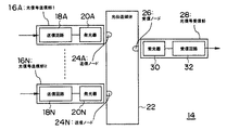
図1は、本発明の第1実施の形態にかかる、光伝送媒体を用いた画像処理装置を含む画像システム10の概略構成を示した。
【0025】
画像システム10は、画像データを入力するための同一種類または異なる種類の複数の画像入力装置(画像データ源)12A〜12Nを備えており、複数の画像入力装置12A〜12Nは画像処理装置14に接続されている。画像処理装置14は、光信号送信部16、シート状の光伝送媒体22及び光信号受信部28を備えている。光信号送信部16は、上記複数の画像入力装置12A〜12Nの入力数を少なくとも含む数に対応する光信号送信部16A〜16Nを備えており、これら光信号送信部16A〜16Nからの光信号が光伝送媒体22において合成され、光信号受信部28へ供給される。光信号受信部28は画像データを出力するための画像出力装置34に接続されている。
【0026】
上記画像入力装置の一例には、原稿などの画像を読み取って画像データを出力するスキャナなどの画像読取装置や、画像を画像データとして受け取ってその画像データを出力するファクシミリ装置などの画像受信装置、蓄積または受信した画像データを出力するコンピュータなどの計算処理装置などがある。また、画像出力装置の一例には、印刷装置や焼き付け装置などの画像データに基づく画像を形成する画像形成装置、画像データを他の装置へ送信する画像送信装置などがある。
【0027】
なお、本実施の形態では、画像入力装置において画像データを電気信号として出力し、その電気信号を光信号送信部において光信号に変換して光伝送媒体に入射する場合を説明するが、本発明はこれに限定されない。例えば、画像入力装置として直接光信号を射出する画像データ源を用いても良い。すなわち、画像入力装置は、画像データを電気信号として出力することに限定されず、画像データを光信号として出力する画像データ源として機能すればよい。この場合、画像データ源からの光信号を光伝送媒体に入力するために、光伝送媒体に直接入力部(後述する送信ノード)を設けても良く、光伝送媒体に光ファイバなどの光伝送路を連結して入力部(後述する送信ノードに連結された光伝送路)としてもよい。
【0028】
図2に示すように、画像処理装置14は、光信号送信部16と、光伝送媒体22と、光信号受信部28から構成されている。光伝送媒体22の一方の端面(図2の左側端面)には、光伝送媒体22へ入力されるべき信号光の入射を担う領域である複数の送信ノード24A〜24Nが形成されており、光伝送媒体22の他方の端面(図2の右側端面)には、光伝送媒体22から出力されるべき信号光の射出を担う領域である受信ノード26とが形成されている。複数の送信ノード24A〜24Nの各々には、光信号送信部16A〜16Nの各々が対応されており、受信ノード26には、光信号受信部28が対応されている。これによって、画像入力装置12からの画像データは光信号送信部で電気信号から光信号に変化され、光伝送媒体22を介した後に、光信号受信部28で光信号から電気信号に変換されて画像出力装置34に出力される。
【0029】
光信号送信部16A〜16Nの各々は、送信回路18A〜18N,及び発光器20A〜20Nを備えている。光信号送信部16Aは、光信号を生成して対応する送信ノード24Aから光伝送媒体22内に光信号を入射する。光信号送信部光信号送信部16Aは、光信号を射出する発光器20Aとその発光器20Aから出射される光信号の基になる電気信号を生成して発光器20Aに送信する送信回路18Aを備えている。発光器20Aから出射した光信号は送信ノード24Aから光伝送媒体22に入射され、その光伝送媒体22内を伝播して受信ノード26から射出される。受信ノード26に対応して光信号受信部28が備えられている。光信号受信部28は、受信ノード26から射出された光信号を電気信号に変換する受光器30、及び受光器30で変換された電気信号を画像出力装置34へ出力する受信回路32を備えている。これにより光信号受信部28の受光器30に入射された光信号は電気信号に変換され、受信回路32により、後段の画像出力装置34に出力される。
【0030】
上記では、発光器20Aから射出される光信号が送信ノード24Aまでの経路を言及していないが、直接カップリングしてもよく、また光コネクタを介して接続してもよい。また、光コネクタを備えたファイバー伝送路を用いて接続してもよい。受信ノード26と受光器30との経路も同様である。なお、他の光信号送信部16B〜16Nの各々についても同様であるため、説明を省略する。
【0031】
なお、画像システム10は、画像入力装置12、光信号送信部16、送信回路18、発光器20、送信ノード24を各々複数備えているが、本実施の形態の説明では、任意の1つを指すときや総称的に用いるとき符号A〜Nを省略する場合があり、また、任意の1つを指すときA〜Nの符号に代えて符号i(A〜Nのうちの何れか1つを表す)、他を指すときj(i≠j:A〜Nのうちの何れか1つの符号)を用いる場合がある。
【0032】
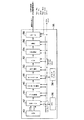
図3には、画像入力装置12としての、原稿上の画像を読み取る画像読取装置の一例を示した。この画像読取装置35は、原稿上の画像を読み取りデジタルデータに変換して出力する。画像読取装置35は、原稿上の画像を読み取るための光電変換素子であるCCDセンサ40を備えており、CCDセンサ40は、CCDインタフェース回路(CCD I/F)42に接続されている。CCDインタフェース回路42は、アナログデジタル変換器(A/D変換器)44,シェーディング補正回路46、デジタルフィルタ48、拡大縮小回路50、AE調整回路52,TRC補正回路54,2値化回路56,及び出力インタフェース回路(出力I/F)58を介して画像データが出力されるように接続されている。画像読取装置35は、CPU36及びタイミングジェネレータ38も備えており、CPU36及びタイミングジェネレータ38は、CCDインタフェース回路42乃至出力インタフェース回路58の各々に対してコマンド及びデータの授受そしてタイミング調整のためのトリガが入出力可能なように、アドレスバス及びデータバスにより接続されている。
【0033】
この画像読取装置35では、原稿上の画像がCCDセンサ40によりアナログの電気信号に変換される。一般にCCDセンサ40からは処理の高速化のために奇数画素と偶数画素の2チャンネルのアナログ信号(EVEN,ODD)が出力される。CCDインタフェース回路42は、図示を省略したが、サンプルホールド回路、アナログアンプ及び合成回路(アナログスイッチ)を含んでいる。CCDインタフェース回路42では、内蔵されたサンプルホールド回路でリセット信号ノイズなどの余分な高調波成分が除去され、この後にアナログアンプで増幅された奇数画素及び偶数画素のアナログ信号がアナログスイッチにより1つの信号に合成されて出力される。
【0034】
またCCDインタフェース回路42では、画像読取装置35ごとの照明光量・CCDセンサ感度・回路のゲインなどのバラツキや、照明ランプの経時的な劣化や装置内汚れなどの経時変化などに影響を受けることなく、次段のA/D変換器44の変換レンジを有効に使うために、図示を省略したオートゲインコントロール回路(AGC回路)について、CCDセンサ40の黒出力を厳密に一定レベルに合わせこむためのオートオフセットコントロール回路(AOC回路)が設けられている。CCDインタフェース回路42より出力されたアナログ信号は、A/D変換器44でジタル信号に変換されて、シェーディング補正回路46以降のデジタル信号処理部に出力される。
【0035】
シェーディング補正回路46では、光学結像系の光量分布の不均一性、CCDセンサ40の画素感度の不均一性、及びCCDセンサ40の暗電流の不均一性などに対する補正が行われる。デジタルフィルタ48では、文字画像の鮮鋭度を上げるためにエッジ強調処理や、網点写真画像のモアレを防ぐために平滑化処理が実行される。すなわちデジタルフィルタ48では、入力画像に応じた画質向上のための処理が実施される。
【0036】
拡大縮小回路50は、読み取り画像のサイズを出力先で要求されるサイズに拡大または縮小する回路であり、ユーザの指示や自動的に拡大縮小処理が実施される。例えば、ユーザの指示による所定範囲(例えば25%から400%の範囲)の指示で拡大及び縮小の処理が実行したり、原稿サイズと出力先で要求されるサイズ(例えばプリンタなどの用紙サイズ)の関係から自動的に拡大率や縮小率(例えば25%から400%)を求めて拡大縮小処理が実行される。
【0037】
AE調整回路52は、原稿の背景濃度の影響を除去するなどの処理を実行する回路である。例えば、AE調整回路52では、新聞紙原稿の文字を読みやすくする処理、すなわち新聞紙原稿のような背景部分が白でない原稿の場合に背景濃度を白にする処理が実施される。TRC補正回路54は、出力先、例えば画像出力装置34の出力階調特性が線形特性(リニア)にする補正を行う。一例として、TRC補正回路54では、プリンタなどの画像出力装置34の出力階調特性がリニアでない場合に、その出力階調特性がリニアになるような補正を行う。また、TRC補正回路54では、原稿の種類に応じて、文字画像はより鮮明になるように、写真画像はより階調性が豊かになるように、トーンカーブの補正処理を実行することができる。
【0038】
2値化回路56は、多値の画像データを2値の画像データに変換する回路であり、例えば、誤差拡散法などの処理により8bit多値であった画像データを1bit2値の画像データに変換する回路である。出力インタフェース回路58は、画像読取装置35の出力先すなわち画像出力装置や画像蓄積装置などの画像データの送信先に応じて、それぞれの装置と同期信号をやりとりして画像データを出力するインタフェース回路である。
【0039】
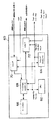
図4には、画像入力装置12として適用できる、図3の画像読取装置に接続可能な画像蓄積装置の一例を示した。この画像蓄積装置60は、図4の例では、画像読取装置35から読み取った画像データをページメモリ66に記憶するものである。画像蓄積装置60は、CPU62,タイミングジェネレータ64,ページメモリ66,ページメモリコントローラ68,入力インタフェース回路(入力I/F)70,出力インタフェース回路(出力I/F)72を備えている。
【0040】
画像蓄積装置60は、1枚または数枚の原稿画像の記憶に用いられる。画像蓄積装置60に入力された画像データは、ページメモリコントローラ68によりアドレスを制御されてページメモリ66に書き込みが実施され、またにページメモリコントローラ68にアドレスを制御されてページメモリ66から画像データの読み出しが実施されて他の装置に出力される。
【0041】
なお、ページメモリ66を利用したその他の機能としては、例えば90°/180°/270°回転のように画像を一定角度回転する画像ローテーション機能や、任意のm枚の原稿画像を1枚の用紙にまとめて印字する機能などがある。
【0042】
次に、図5、図6、図7を参照して、上記構成の画像読取装置35から画像蓄積装置60に画像データを取り込んで記憶させる場合の動作を説明する。本実施の形態では、画像読取装置35と画像蓄積装置60の間でやり取りされる同期信号は、nPage Req信号、nLine Req信号、nValid信号、VCLK信号の4種類である。
【0043】
まず、副走査方向の同期を取るために、画像蓄積装置(ページメモリ)60から画像読取装置35に対してnLine Req信号とnLine Req信号の立ち下がり(図6の状態t1)に同期して、アクティブになるnPage Req信号が出力される。このnPage Req信号は、副走査方向において画像データが有効な期間中はアクティブとなり、ハイレベル信号(以下、High)からローレベル信号(以下、Low)になる。
【0044】
また、nLine Req信号は画像読取装置35と画像蓄積装置60との間の同期をとるためだけに用いられるので必ずしも有効な画像データの範囲と一致している必要はない。この動作に応じて画像読取装置35から画像蓄積装置60に対してnValid信号が出力される。さらに、画像読取装置35からは、主査方向の同期をとるためのVCLK信号とこの信号の立ち上がり(図7の状態t2)に同期した画像データ(VDATA)が出力される。
【0045】
このとき、nValid信号は画像データ同様にVCLK信号の立ち上がり(図7の状態t3)に同期しており、HighからLowに変化したアクティブな期間は画像データの有効範囲を示している。このような同期信号及び画像データのやり取りにより、画像読取装置35から画像蓄積装置60へ、合成処理が実施されるテンプレート用のフォーマット画像の記憶が可能となる。
【0046】
次に、図8、図9、図10を用いて、画像読取装置35および画像蓄積装置60から画像出力装置34に同時に画像データを転送する場合の動作を説明する。本実施の形態では、画像読取装置35およびページメモリを含む画像蓄積装置60と、画像出力装置34との間でやり取りされる同期信号は、Page Sync信号、Line Sync信号、VCLK信号の3種類である。
【0047】
ここでは、画像読取装置35の出力側は、光信号送信部16iに接続され、画像蓄積装置60の出力側は、光信号送信部16jに接続されている。光信号送信部16i及び光信号送信部16jに入力された画像信号は、光伝送媒体22で合成されて、光信号受信部28から画像出力装置34へ出力される。画像出力装置34は、入力インタフェース回路(入力I/F)74及びタイミングジェネレータ76を備えており、光信号受信部28からの画像データをタイミングジェネレータ76により同期しつつ入力インタフェース回路74で入力する。
【0048】
まず、副走査方向の同期を取るために、画像出力装置34から画像読取装置35および画像蓄積装置60に対してLine Sync信号とLine Sync信号の立ち下がり(図9の状態t4)に同期して、アクティブになるPage Sync信号が出力される。
【0049】
このときPage Sync信号は、副走査方向において画像データが有効な期間中はアクティブとなりLowからHighになる。また、Line Sync信号は画像読取装置35および画像蓄積装置60と、画像出力装置34との間の同期(図10のVCLK信号の立ち下がり(状態t5)に同期)をとると共に、LowからHighに変化したアクティブな期間で有効な画像データの範囲を示している。さらに、画像出力装置34から画像読取装置35および画像蓄積装置60に対して、主走査方向の同期をとるVCLK信号が出力される。
【0050】
この動作に応じて、画像読取装置35および画像蓄積装置60から画像出力装置34に対して、Line Sync信号の立上がりから1/2クロックだけ遅れたVCLK信号の立ち上り(図10の状態t6)に同期してかつこの画素を有効画像データの先頭画素とする画像データ(VDATA1及びVDATA2)がそれぞれ出力される。このとき、Line Sync信号は画像データ同様にVCLK信号の立ち下がり(図10の状態t7)に同期しており、HighからLowに変化したアクティブな期間は画像データの有効範囲を示している。このような同期信号及び画像データのやり取りにより、画像読取装置35および画像蓄積装置60から同時に画像出力装置34への画像データの転送が可能となる。
【0051】
次に、図11、図12を用いて、画像読取装置35から出力される画像データ(VDATA1)と画像蓄積装置60から出力される画像データ(VDATA2)が光伝送媒体22を経由して合成されて画像出力装置34に取り込まれるまでの動作を説明する。
【0052】
画像出力装置34から出力されるVCLK信号に同期して画像読取装置35から出力される画像データ(VDATA1)と、同様にVCLK信号に同期して画像蓄積装置60から出力される画像データ(VDATA2)は、それぞれ光信号送信部16i、16j内で電気信号から光信号に変換されて、対応する送信ノード24i、24jより光伝送媒体22内に出射される。
【0053】
光伝送媒体22内にそれぞれ出射された光信号は、図12に示すように(合成VDATA)、合成された光信号となって、受信ノード26より光信号受信部28に出射される。光信号受信部28内の受光器30で光信号から電気信号に変換された合成画像データ(合成VDATA)は、受信回路32で2値化されて画像出力装置34に送られる。このとき、画像読取装置35から出力された画像データ(VDATA1)と画像蓄積装置60から出力された画像データ(VDATA2)を、それぞれ光信号送信部16i、16jで光信号に変換するときの光強度は任意の強度で構わないものとする。そして、受信回路32で2値化するときには、それぞれの光信号を2値化するのに必要な閾値のうち、値の小さい閾値Thを用いれば合成された光信号の2値化が可能である。画像出力装置34に送られた合成画像データは、入力インタフェース回路74においてVCLK信号でラッチされて、画像出力装置34内の次段の処理部へ送られる。
【0054】
図13は、別の画像と合成して出力させたいフォーマット画像G1を画像読取装置35から読み取って一時的に画像蓄積装置60に記憶しておき、次に画像読取装置35から読み取った画像G2と合成して得た合成画像G3を画像出力装置34から出力したときの、各画像G1,G2,G3を示した一例である。
【0055】
図14は、機密文書等を出力する際に予め内蔵してある「禁複写」や「回覧注意」といたデータを付加したり、多枚数の出力をする際にページナンバーなどの情報を付加したり、あるいは日付情報を付加することが可能なアノテーション用の画像蓄積装置60の画像G4と、画像読取装置35から読み取った画像G5とを合成して得た画像G6を画像出力装置34から出力したときの、各画像G4,G5,G6を示した一例である。
【0056】
図15は、上記図14に示すアノテーション用画像を付加可能にするための、画像蓄積装置60の構成の一例を示したものである。ここでは、画像蓄積装置60は、「禁複写」や「回覧注意」といた既製文字列、図示しない操作パネルよりオペレータが入力した任意の文字列、ページナンバーや日付情報を記憶するためのアノテーションメモリ78、アノテーションメモリ78に対して該当するデータを入出力するコントローラであるメモリコントローラ80,文字データに対する任意のフォントを記憶したフォントROM82を備えている。フォントROM82はCPU62に接続されており、メモリコントローラ80はアノテーションメモリ78、出力インタフェース回路72、CPU62、タイミングジェネレータ64に接続されている。また、アノテーションメモリ78は、CPU62及びタイミングジェネレータ64にも接続されている。
【0057】
実際の作動では、図示しない操作パネルからの指示に応じて、CPU62により必要な文字列のデータがフォントROM82から読み出され、展開されてアノテーションメモリ78に書き込まれる。読み出し時は書き込み時とは異なりメモリコントローラ80にアドレスを制御されてメモリコントローラ80から文字列のデータの読み出しが実施されて他の装置に出力される。
【0058】
図16は、画像蓄積装置60としてハードディスク84を備えた一例をブロック図として示した。図16の例では、画像読取装置35から読み取った画像データをハードディスクに記憶する画像蓄積装置60の一例を示したものである。ハードディスク84は、数枚から数十枚の原稿画像の記憶に用いられる。ここでは、画像蓄積装置60は、画像データを記憶するためのハードディスク84、ハードディスク84に対して該当する画像データを入出力するコントローラであるハードディスクコントローラ86を備えている。ハードディスクコントローラ86はCPU62、ハードディスク84、入力インタフェース回路70、出力インタフェース回路72、タイミングジェネレータ64に接続されている。
【0059】
上記ハードディスク84を利用したその他の機能としては、1回の原稿スキャンで丁合いされたセットを複数(例えばN部)プリントする電子ソート機能や、小冊子を作成するシグニチャ機能などがある。画像蓄積装置に入力された画像データは、ハードディスクコントローラ86により例えばUltra ATAのような汎用の転送方式を利用してハードディスク84に書き込みが実施され、また同様にハードディスクコントローラ86によりハードディスク84から画像データの読み出しが実施されて他の装置に出力される。
【0060】
また、ハードディスク84に画像を書き込むときに、画像圧縮を行いデータ容量を減らしたのちに行うこともできる。本画像蓄積装置60では、ページメモリを利用した画像蓄積装置と同様に、別の画像と合成して出力させたいフォーマット画像を画像読取装置から読み取って一時的に記憶しておき、次に画像読取装置から読み取った画像と合成して画像出力装置から出力するというような図13に示す処理に利用することが可能である。
【0061】
なお、画像入力装置として本発明システムに接続可能な装置としては、上記で説明してきた画像読取装置35や画像蓄積装置60のほかに、パーソナルコンピュータなどで扱う画像データをネットワーク等を介して受信し、編集・加工・蓄積するコントローラ装置、電話回線等を介して画像データの送受信を行うFAX装置がある。コントローラ装置を接続することで、例えばパーソナルコンピュータ等で作成した任意の画像データを一旦用紙に印字して出力することなく、画像読取装置で読み込んだ原稿の画像データとの合成処理が可能となる。同様にFAX装置を接続することで、受信した任意の画像データを一旦用紙に印字して出力することなく、画像読取装置で読み込んだ原稿の画像データとの合成処理が可能となる。
【0062】
〔第2実施の形態〕
図17には、本発明の第2実施の形態にかかる、光伝送媒体を用いた画像処理装置を含む画像システム11の概略構成を示した。本実施の形態の画像システム11は、上記実施の形態の画像システム10の画像読取装置35や画像出力装置34などより小さい回路ブロックやASICなどを対象としてものである。
【0063】
本実施の形態の画像システム11は、画像データを入力するための同一種類または異なる種類の複数の回路ブロック88A〜88Nを備えており、複数の回路ブロック88A〜88Nは画像処理装置14に接続されている。画像処理装置14は、光信号送信部16、シート状の光伝送媒体22及び光信号受信部28を備えている。光信号送信部16は、上記複数の回路ブロック88A〜88Nに対応する光信号送信部16A〜16Nを備え、これらの光信号が光伝送媒体22において合成され、光信号受信部28へ供給され、光信号受信部28は画像データを出力するための回路ブロック90に接続されている。
【0064】
このように、本実施の形態では、画像入力装置や画像出力装置として小さい回路ブロックやASICなどを利用できるので、よりコンパクトな回路構成を実現できる。
【0065】
〔第3実施の形態〕
図18には、本発明の第3実施の形態にかかる、光伝送媒体を用いた画像処理装置を含む画像システム11Aの概略構成を示した。本実施の形態では、画像入力装置として2つのデジタルフィルタ回路を用いて画像処理を行う場合に本発明を適用したものである。
【0066】
本実施の形態では、画像入力装置に対応する部分として、2種類の画像データを出力するために、第1デジタルフィルタ91、第2デジタルフィルタ92、及び文字写真分離回路94を含んで構成されている。画像処理装置14の出力側には、後段の画像処理ブロック96が接続されている。
【0067】
第1デジタルフィルタ91には原稿内の文字画像に対して最適な画像処理がされるようなパラメータ設定がされており、入力された画像データを、後述する文字写真分離回路94で指定された文字画像領域に対して画像処理した画像データを光信号送信部16Aへ出力するように接続されている。第2デジタルフィルタ92には原稿内の写真画像に対して最適な画像処理がされるようなパラメータ設定がされており、入力された画像データを、後述する文字写真分離回路94で指定された写真画像領域に対して画像処理した画像データを光信号送信部16Bへ出力するように接続されている。
【0068】
文字写真分離回路94は、第1デジタルフィルタ91及び第2デジタルフィルタ92の各々に接続されており、文字写真分離回路94では、入力された画像データについて、原稿内の文字画像と写真画像の分離を行う。分離結果として、例えば文字画像領域では「L」レベル(LOW)となり、写真画像領域では「H」レベル(HIGH)となる像域分離信号が出力される。この像域分離信号が、第1デジタルフィルタ91及び第2デジタルフィルタ92のアクティブ信号となり、「L」レベルのときは第1デジタルフィルタ91がアクティブとなり原稿内の文字画像に対して最適な処理が行われた画像が出力され、また「H」レベルのときは第2デジタルフィルタ92がアクティブとなり原稿内の写真画像に対して最適な処理が行われた画像が出力さる。
【0069】
この場合、第1デジタルフィルタ91及び第2デジタルフィルタ92と後段の画像処理ブロック96との同期信号のやり取りは、上述の図9および図10と同様にPage Sync信号、Line Sync信号、VCLK信号の3種類を用いた方法で行われる。画像データは例えば8bitで構成される多値データであるので、図2で示されるような光伝送媒体と複数の光信号送信部と光信号受信部で構成される光信号合成ブロックが8層構造とすることができる。
【0070】
なお、このような積層構造の画像処理装置14に本発明は限定さなない。すなわち、単層構造でも利用可能である。この場合、入力された8ビット信号をパラレル信号として、入力側でそのパラレル信号をシリアル信号に変換し、出力側でシリアル信号をパラレル信号に変換することにより容易に適用が可能である。
【0071】
次に、図19、図20を用いて、本実施の形態にかかる画像システム11Aの動作を説明する。ここでは、第1デジタルフィルタ91から出力される画像データ(VDATA1)と第2デジタルフィルタ92から出力される画像データ(VDATA2)が光伝送媒体22を経由して合成されて後段の画像処理ブロック96に取り込まれるまでの動作について説明する。なお、第1デジタルフィルタ91及び第2デジタルフィルタ92から出力される画像データは8bit構成の場合について説明するが、以下の説明を簡単にするため、最下位のbit0に着目して説明する。
【0072】
文字写真分離回路94から出力される像域分離信号が「L」レベルときは文字画像領域を示しているので、第1デジタルフィルタ91から有効な画像データが出力され、第2デジタルフィルタ92からは常に「L」レベルの画像データが出力される。
【0073】
一方、文字写真分離回路94からの像域分離信号が「H」レベルときは写真画像領域を示しているので、第1デジタルフィルタ91から常に「L」レベルの画像データが出力され、第2デジタルフィルタ92からは有効な画像データが出力される。このとき用いられる像域分離信号は、文字写真分離回路94と第1デジタルフィルタ91及び第2デジタルフィルタ92のそれぞれの画像データの遅延量を考慮しているものとする。
【0074】
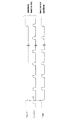
後段の画像処理ブロック96から出力されるVCLK信号に同期して第1デジタルフィルタ91から出力される画像データ(VDATA1-bit0)と、同様にVCLK信号に同期して第2デジタルフィルタ92から出力される画像データ(VDATA2-bit0)は、それぞれ光信号送信部16A、16B内で電気信号から光信号に変換されて、対応する送信ノード24A,24Bより光伝送媒体22内に出射される。光伝送媒体22内にそれぞれ出射された光信号は、図20に示すように合成された光信号となって、受信ノード26より光信号受信部28に出射される。
【0075】
光信号受信部28内の受光器30で光信号から電気信号に変換された合成画像データ(合成VDATA-bit0)は、受信回路32で2値化されて後段の画像処理ブロック96に送られる。このとき、第1デジタルフィルタ91から出力された画像データ(VDATA1-bit0)と第2デジタルフィルタ92から出力された画像データ(VDATA2-bit0)を、それぞれ光信号送信部で光信号に変換するときの光強度は任意の強度で構わないものとする。
【0076】
そして受信回路32で2値化するときには、それぞれの光信号を2値化するのに必要な閾値のうち、値の小さい閾値を用いれば合成された光信号の2値化が可能である。後段の画像処理ブロック96に送られた合成画像データは、VCLK信号でラッチされてから後段の画像処理ブロック96内で使用される。
【0077】
【発明の効果】
以上の説明のように、本発明によれば、信号が高速化しても電磁ノイズの発生を抑えることが可能であると共に、接続される画像データ源が増加しても回路規模が大きくならず、かつコストの上昇を抑えることができる、という効果がある。
【図面の簡単な説明】
【図1】 本発明の第1実施の形態の概略構成を示すブロック図である。
【図2】 光信号を扱う基本構成を示すブロック図である。
【図3】 原稿上の画像をデジタルデータに変換する画像読取装置のブロック図である。
【図4】 画像データをページメモリに記憶する画像蓄積装置のブロック図である。
【図5】 画像読取装置から画像蓄積装置に画像データを取り込む場合の画像データ及び同期信号の流れを示したブロック図である。
【図6】 画像読取装置から画像蓄積装置に画像データを取り込む場合の副走査方向の同期信号のタイミングチャートである。
【図7】 画像読取装置から画像蓄積装置に画像データを取り込む場合の主走査方向の同期信号のタイミングチャートである。
【図8】 光伝送媒体を介して画像データを合成するときの画像データと同期信号の流れを示したブロック図である。
【図9】 画像読取装置及び画像蓄積装置から画像出力装置に画像データを転送する場合の副走査方向の同期信号のタイミングチャートである。
【図10】 画像読取装置及び画像蓄積装置から画像出力装置に画像データを転送する場合の主走査方向の同期信号のタイミングチャートである。
【図11】 画像読取装置からの画像データと画像蓄積装置からの画像データを合成するときの流れを示すタイミングチャートである。
【図12】 光伝送媒体内で光信号に変換された2つの画像データを合成するときの波形データを示した信号図である。
【図13】 第1実施の形態にかかり、画像読取装置と画像蓄積装置を利用したときの画像の合成及びその過程を示す説明図である。
【図14】 第1実施の形態にかかり、画像読取装置と画像蓄積装置(アノテーション)を利用したときの画像の合成及びその過程を示す説明図である。
【図15】 画像データを記憶するアノテーション用の画像蓄積装置の概略構成を示すブロック図である。
【図16】 画像データをハードディスクに記憶する画像蓄積装置の概略構成を示すブロック図である。
【図17】 本発明の第2実施の形態にかかる画像システムの概略構成を示すブロック図である。
【図18】 本発明の第3実施の形態にかかる画像システムの画像処理部の概略構成を示すブロック図である。
【図19】 第1デジタルフィルタからの画像データと第2デジタルフィルタからの画像データを合成するときの流れを示すタイミングチャートである。
【図20】 光伝送媒体内で光信号に変換された第1デジタルフィルタと第2デジタルフィルタの画像データ(bit0)を合成するときの波形データを示した信号図である。
【符号の説明】
10…画像システム
12…画像入力装置
14…画像処理装置
16…光信号送信部
18…送信回路
20…発光器
22…光伝送媒体
24…送信ノード
26…受信ノード
28…光信号受信部
30…受光器
32…受信回路
34…画像出力装置
35…画像読取装置[0001]
BACKGROUND OF THE INVENTION
The present invention relates to an image processing apparatus, and more particularly to an image processing apparatus that performs signal processing and image processing including transmission of an optical signal through an optical transmission medium.
[0002]
[Prior art]
In image processing apparatuses that handle digital signals, such as digital copying machines, various image processing apparatuses that synthesize and output a plurality of images have been proposed. For example, in the technique disclosed in Japanese Patent Laid-Open No. 5-308508, one or more original images are stored in a storage unit as a background pattern, and the background pattern is input as a format image from an image input unit such as a scanner. There has been proposed an image processing apparatus that combines with a document image and outputs the combined result by output means. Japanese Patent Application Laid-Open No. 8-23438 has proposed an image processing apparatus that synthesizes an image input from a scanner and an image input from an external device such as a computer. Further, in the technique disclosed in Japanese Patent Laid-Open No. 5-22568, when a confidential document is distributed as a conference material or the like, different characters such as serial numbers are printed on a plurality of copies of the same manuscript, and the combination of the recipient and the character An apparatus has been proposed that keeps secrets and keeps secret information by ascertaining the source of the leakage. Japanese Patent Application Laid-Open No. 8-18767 discloses an image processing apparatus that selects a desired one from a plurality of types of pre-registered stamp images and prints the selected stamp image superimposed on a read image. Has been proposed.
[0003]
[Problems to be solved by the invention]
However, in the above conventional technique, the circuit for synthesizing the input image such as the original image and the other input image such as the format image, the character, or the stamp image is composed of a logic circuit, so that the signal speed can be increased. As a result, generation of electromagnetic noise (EMI) becomes a problem. Further, every time the number of image input means to be connected increases, a large number of connection connectors and harnesses are required, which raises a problem of an increase in the cost of the connection means. Furthermore, as the number of connected image input devices increases, the circuit scale of the circuit that performs synthesis increases.
[0004]
In view of the above circumstances, the present invention provides a low-cost image processing apparatus that reduces electromagnetic noise and does not increase the circuit scale while speeding up signals when image processing is performed using an optical transmission method. Objective.
[0005]
[Means for Solving the Problems]
In order to achieve the above object, an image processing apparatus according to the present invention combines an input image data to synthesize a plurality of images and outputs image data based on an electrical signal corresponding to the synthesized image. In It is one of an optical coupler that transmits an optical signal and an optical sheet medium that is formed into a sheet and transmits an optical signal, Input from each of multiple image data sources Represents the pixel location and density on the image A transmission medium for synthesizing a plurality of images by optical calculation for synthesizing each of the image data based on the plurality of input optical signals, and a combined image obtained by synthesizing the images by the transmission medium. And an optical signal receiving means for transmitting the received optical signal to an image output device for converting the received optical signal into image data by an electrical signal and outputting the image data as image data. And
[0006]
In the present invention, the image processing apparatus combines a plurality of images by combining the input image data, and outputs image data based on an electrical signal corresponding to the combined image. In the image processing apparatus according to the present invention, a plurality of images are synthesized by optical computation that synthesizes image data based on optical signals input from each of a plurality of image data sources in a transmission medium. In the transmission medium, the optical signal from the image data source may be input from a transmission path such as an optical fiber connected to a combining unit that combines image data based on the input optical signal. Further, an optical signal may be input directly to the transmission medium. The optical signal synthesized by the optical calculation is received by the optical signal receiving means, and at the same time, the received optical signal is converted into image data by an electrical signal. Image data corresponding to the combined image of the optical signals combined by this optical calculation is transmitted to the image output device.
[0007]
As a result, even if the signal speed is increased, computation by image processing can be achieved by optical computation using an optical signal, so that generation of electromagnetic noise can be suppressed, and the circuit scale can be increased even if the number of connected image data sources increases. Is not increased, and an increase in cost can be suppressed.
[0008]
As the transmission medium, any one of an optical coupler that transmits an optical signal and an optical sheet medium that is formed in a sheet shape and transmits an optical signal can be adopted. By adopting either one of the optical coupler and the optical sheet medium, the optical signal is optically calculated only by being propagated through the optical coupler or the optical sheet medium, thereby simplifying the synthesis process as image processing.
[0009]
The transmission medium is a predetermined part of the synthesis process. The light calculation is not limited to being applied to all image processing, and can be applied to part of the processing. For example, it is possible to adopt the optical calculation only for processing with a large calculation load. By doing in this way, the freedom degree of the application range of image processing can be increased.
[0010]
The image data represents pixel positions and densities on the image. Some image data represents an image in units of pixels, that is, so-called bitmap data representing the position and density of a pixel on the image, and some represents the image by the image data itself by processing the entire image. In this case, by representing the position and density of the pixel on the image, the image data can be synthesized in units of pixels, and a plurality of images can be processed by simple synthesis in units of pixels.
[0011]
The image output apparatus may employ a printing apparatus that prints an image based on the image data. In the printing apparatus, there is a case where image processing for inserting and printing an insertion image or a format image is executed as the preceding processing. Therefore, by adopting a printing device as the image output device, it is possible to synthesize a plurality of images with the printed matter that is the output, and it is possible to synthesize and print a user-specified or predetermined image. .
[0012]
At least one of the image data sources can include an optical signal transmission unit that converts image data input as an electrical signal into an optical signal and transmits the optical signal.
[0013]
In the image processing apparatus, a plurality of images can be combined by image processing such as combining image data based on input electrical signals, and image data based on electrical signals corresponding to the combined images can be output. Therefore, a plurality of optical signal transmission means are provided. Each of the optical signal transmitting means converts image data based on an electrical signal input from an image data source such as an image input device for inputting image data based on an electrical signal into an optical signal and transmits the optical signal. As a result, at least one electrical signal input as image data is transmitted as an optical signal in the optical signal transmission means, and a plurality of images are synthesized by an optical operation for synthesizing the plurality of optical signals by the transmission medium.
[0014]
As a result, even if the electrical signal speeds up, the calculation by image processing can be achieved by the optical calculation by the optical signal, so it is possible to suppress the generation of electromagnetic noise, and the circuit even if the number of connected image input means increases The scale does not increase and the increase in cost can be suppressed.
[0015]
At least one of the image data sources can use an image reading device that converts a document image into image data based on an electrical signal using a photoelectric conversion element in order to convert the document image into a digital image. As an example of the image reading apparatus, there is an apparatus that converts a document image into a digital image using a photoelectric conversion element such as a CCD, and processing for easily combining the digital image that has been read and converted can be performed.
[0016]
At least one of the image data sources may employ a controller device that is connected to a network configured to exchange image data and that performs at least one process of editing, processing, and storing image data. As a device that requests image processing, there is a controller device that edits or processes image data and stores the result. If this controller device is used as an image data source, it is possible to easily perform image processing, which is composition processing. This controller device includes a controller device that receives image data handled by a personal computer or the like via a network and edits, processes, and stores the image data.
[0017]
At least one of the image data sources can use an image storage device that stores image data in a storage means. For example, by employing an image storage device that stores image data using a storage unit such as a hard disk or a semiconductor memory, the image data can be easily taken out and stored.
[0018]
At least one of the image data sources can employ a facsimile apparatus that outputs communication data received from a communication line as electronic image data as image data. A facsimile apparatus is an apparatus that receives and transmits an image via a communication line. By adding another image, for example, a format image, to the image to be received or transmitted, an added value can be added to the image to be received or transmitted.
[0019]
At least one of the image data sources is at least one image processing block that outputs image data based on electrical signals among a plurality of image processing blocks that perform image processing on image data based on electrical signals. The image data source is not limited to one device. That is, one image processing block when image processing is classified into a plurality of functions can be associated. Thereby, the optical calculation can be adopted for any arbitrary image processing block among the plurality of image processing blocks.
[0020]
A plurality of the image processing blocks are provided as the image data source, and the plurality of image processing blocks are image processing blocks having the same image processing function and executing different image processing with different operation parameters. . Even if the image processing block has the same function, different image processing may be performed by changing the operation parameter. Therefore, the degree of freedom of image processing can be increased by associating image processing blocks having the same image processing function and executing different image processing with different operation parameters with the image data source.
[0021]
A plurality of the image processing blocks are provided as the image data source, and the plurality of image processing blocks are image processing blocks having different image processing functions. Image processing apparatuses often have different image processing functions. Therefore, by combining an image processing block that executes different image processing functions with an image data source, it is possible to perform composition by arbitrary image processing.
[0022]
The image output device is an image processing block that performs image processing on image data based on electrical signals. The image data obtained by combining as described above is not limited to a device that only outputs an image, and may be processed further downstream. Therefore, by using an image processing block as the image output device, it is possible to easily transmit image data to downstream processing.
[0023]
DETAILED DESCRIPTION OF THE INVENTION
Hereinafter, an example of an embodiment of the present invention will be described in detail with reference to the drawings.
[0024]
[First embodiment]
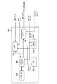
FIG. 1 shows a schematic configuration of an
[0025]
The
[0026]
Examples of the image input device include an image reading device such as a scanner that reads an image of a document and outputs image data, an image receiving device such as a facsimile device that receives an image as image data and outputs the image data, There is a calculation processing device such as a computer that outputs stored or received image data. Examples of the image output apparatus include an image forming apparatus that forms an image based on image data, such as a printing apparatus or a printing apparatus, and an image transmission apparatus that transmits image data to another apparatus.
[0027]
In the present embodiment, image data is output as an electrical signal in the image input device, and the electrical signal is converted into an optical signal in the optical signal transmission unit and incident on the optical transmission medium. Is not limited to this. For example, an image data source that directly emits an optical signal may be used as the image input device. That is, the image input device is not limited to outputting image data as an electrical signal, but may function as an image data source that outputs image data as an optical signal. In this case, in order to input an optical signal from the image data source to the optical transmission medium, an input unit (a transmission node to be described later) may be directly provided in the optical transmission medium, and an optical transmission line such as an optical fiber is provided in the optical transmission medium. May be connected to form an input unit (an optical transmission line connected to a transmission node described later).
[0028]
As shown in FIG. 2, the
[0029]
Each of the optical
[0030]
In the above description, the optical signal emitted from the
[0031]
The
[0032]
FIG. 3 shows an example of an image reading device that reads an image on a document as the
[0033]
In the
[0034]
Further, the
[0035]
The
[0036]
The enlargement /
[0037]
The
[0038]
The
[0039]
FIG. 4 shows an example of an image storage device that can be applied as the
[0040]
The
[0041]
As other functions using the
[0042]
Next, with reference to FIGS. 5, 6, and 7, an operation when image data is captured and stored in the
[0043]
First, in order to synchronize in the sub scanning direction, the image storage device (page memory) 60 synchronizes with the falling of the nLine Req signal and the nLine Req signal (state t1 in FIG. 6) from the
[0044]
Further, since the nLine Req signal is used only for synchronization between the
[0045]
At this time, the nValid signal is synchronized with the rising edge of the VCLK signal (state t3 in FIG. 7) like the image data, and the active period changed from High to Low indicates the effective range of the image data. By exchanging the synchronization signal and the image data as described above, it is possible to store the format image for the template to be combined from the
[0046]
Next, an operation when image data is simultaneously transferred from the
[0047]
Here, the output side of the
[0048]
First, in order to synchronize in the sub-scanning direction, the
[0049]
At this time, the Page Sync signal becomes active and changes from Low to High during a period in which the image data is valid in the sub-scanning direction. The Line Sync signal synchronizes between the
[0050]
In accordance with this operation, the
[0051]
Next, the image data (VDATA1) output from the
[0052]
Image data (VDATA1) output from the
[0053]
As shown in FIG. 12 (combined VDATA), the optical signals respectively emitted into the
[0054]
FIG. 13 shows a format image G1 to be combined with another image and output from the
[0055]
In FIG. 14, data such as “prohibited copying” and “circulation warning” that are built in in advance when outputting confidential documents are added, or information such as page numbers is added when outputting a large number of sheets. The
[0056]
FIG. 15 shows an example of the configuration of the
[0057]
In actual operation, in accordance with an instruction from an operation panel (not shown), necessary character string data is read from the
[0058]
FIG. 16 shows an example in which a
[0059]
Other functions using the
[0060]
Also, when an image is written to the
[0061]
As an image input device that can be connected to the system of the present invention, in addition to the
[0062]
[Second Embodiment]
FIG. 17 shows a schematic configuration of an
[0063]
The
[0064]
Thus, in this embodiment, since a small circuit block, ASIC, or the like can be used as the image input device or the image output device, a more compact circuit configuration can be realized.
[0065]
[Third Embodiment]
FIG. 18 shows a schematic configuration of an image system 11A including an image processing apparatus using an optical transmission medium according to the third embodiment of the present invention. In this embodiment, the present invention is applied when image processing is performed using two digital filter circuits as an image input device.
[0066]
In the present embodiment, the first digital filter 91, the second
[0067]
The first digital filter 91 is set with parameters so that optimum image processing is performed on the character image in the document, and the input image data is converted into the character designated by the character /
[0068]
The character /
[0069]
In this case, the synchronization signal exchange between the first digital filter 91 and the second
[0070]
The present invention is not limited to the
[0071]
Next, the operation of the image system 11A according to the present embodiment will be described with reference to FIGS. Here, the image data (VDATA 1) output from the first digital filter 91 and the image data (VDATA 2) output from the second
[0072]
When the image area separation signal output from the character
[0073]
On the other hand, when the image area separation signal from the character /
[0074]
Image data (VDATA1-bit0) output from the first digital filter 91 in synchronization with the VCLK signal output from the subsequent image processing block 96, and similarly output from the second
[0075]
The synthesized image data (synthesized VDATA-bit0) converted from the optical signal to the electrical signal by the
[0076]
When binarization is performed by the receiving
[0077]
【The invention's effect】
As described above, according to the present invention, it is possible to suppress the generation of electromagnetic noise even when the signal speed increases, and the circuit scale does not increase even if the number of connected image data sources increases. In addition, there is an effect that an increase in cost can be suppressed.
[Brief description of the drawings]
FIG. 1 is a block diagram showing a schematic configuration of a first embodiment of the present invention.
FIG. 2 is a block diagram showing a basic configuration for handling an optical signal.
FIG. 3 is a block diagram of an image reading apparatus that converts an image on a document into digital data.
FIG. 4 is a block diagram of an image storage device that stores image data in a page memory.
FIG. 5 is a block diagram illustrating a flow of image data and a synchronization signal when image data is captured from the image reading apparatus to the image storage apparatus.
FIG. 6 is a timing chart of synchronization signals in the sub-scanning direction when image data is captured from the image reading apparatus to the image storage apparatus.
FIG. 7 is a timing chart of synchronization signals in the main scanning direction when image data is captured from the image reading apparatus to the image storage apparatus.
FIG. 8 is a block diagram illustrating a flow of image data and a synchronization signal when image data is combined via an optical transmission medium.
FIG. 9 is a timing chart of synchronization signals in the sub-scanning direction when image data is transferred from the image reading device and the image storage device to the image output device.
FIG. 10 is a timing chart of synchronization signals in the main scanning direction when image data is transferred from the image reading apparatus and the image storage apparatus to the image output apparatus.
FIG. 11 is a timing chart showing a flow when the image data from the image reading device and the image data from the image storage device are combined.
FIG. 12 is a signal diagram showing waveform data when two image data converted into optical signals in an optical transmission medium are combined.
FIG. 13 is an explanatory diagram illustrating image synthesis and a process when an image reading apparatus and an image storage apparatus are used according to the first embodiment.
FIG. 14 is an explanatory diagram illustrating image synthesis and the process when an image reading device and an image storage device (annotation) are used according to the first embodiment;
FIG. 15 is a block diagram illustrating a schematic configuration of an image storage device for annotation that stores image data.
FIG. 16 is a block diagram illustrating a schematic configuration of an image storage device that stores image data in a hard disk.
FIG. 17 is a block diagram showing a schematic configuration of an image system according to a second embodiment of the present invention.
FIG. 18 is a block diagram illustrating a schematic configuration of an image processing unit of an image system according to a third embodiment of the present invention.
FIG. 19 is a timing chart showing a flow when the image data from the first digital filter and the image data from the second digital filter are combined.
FIG. 20 is a signal diagram showing waveform data when combining image data (bit 0) of the first digital filter and the second digital filter converted into an optical signal in the optical transmission medium.
[Explanation of symbols]
10. Image system
12. Image input device
14 Image processing apparatus
16: Optical signal transmitter
18 ... Transmission circuit
20 ... Light emitter
22: Optical transmission medium
24 ... Sending node
26: Receiving node
28: Optical signal receiver
30 ... Receiver
32. Receiving circuit
34. Image output device
35. Image reading device
Claims (12)
光信号を伝送する光カプラ及びシート状に形成されかつ光信号を伝送する光シート媒体の何れか一方であると共に、複数の画像データ源の各々から入力された画像上の画素の位置及び濃度を表す光信号による各々の画像データが入力され、前記入力された複数の光信号による各々の画像データを合成する光演算により複数の画像を合成する伝送媒体と、
前記伝送媒体により画像合成された合成画像に対応する光信号を、受信すると共に、受信した光信号を電気信号による画像データに変換しかつ画像データとして出力するための画像出力装置へ送信する光信号受信手段と、
を備えたことを特徴とする画像処理装置。In an image processing apparatus that synthesizes a plurality of images by synthesizing input image data and outputs image data based on an electrical signal corresponding to the synthesized image,
It is either an optical coupler that transmits an optical signal or an optical sheet medium that is formed in a sheet shape and transmits an optical signal, and the position and density of a pixel on an image input from each of a plurality of image data sources. a transmission medium for combining a plurality of images by optical calculation, each of the image data by the optical signal is input, to synthesize each image data according to the inputted plurality of optical signals representing,
An optical signal for receiving an optical signal corresponding to a synthesized image synthesized by the transmission medium and transmitting the received optical signal to an image output device for converting the received optical signal into image data using an electrical signal and outputting the image data as image data. Receiving means;
An image processing apparatus comprising:
Priority Applications (1)
| Application Number | Priority Date | Filing Date | Title |
|---|---|---|---|
| JP2002170951A JP3960136B2 (en) | 2002-06-12 | 2002-06-12 | Image processing device |
Applications Claiming Priority (1)
| Application Number | Priority Date | Filing Date | Title |
|---|---|---|---|
| JP2002170951A JP3960136B2 (en) | 2002-06-12 | 2002-06-12 | Image processing device |
Publications (2)
| Publication Number | Publication Date |
|---|---|
| JP2004023112A JP2004023112A (en) | 2004-01-22 |
| JP3960136B2 true JP3960136B2 (en) | 2007-08-15 |
Family
ID=31170936
Family Applications (1)
| Application Number | Title | Priority Date | Filing Date |
|---|---|---|---|
| JP2002170951A Expired - Fee Related JP3960136B2 (en) | 2002-06-12 | 2002-06-12 | Image processing device |
Country Status (1)
| Country | Link |
|---|---|
| JP (1) | JP3960136B2 (en) |
-
2002
- 2002-06-12 JP JP2002170951A patent/JP3960136B2/en not_active Expired - Fee Related
Also Published As
| Publication number | Publication date |
|---|---|
| JP2004023112A (en) | 2004-01-22 |
Similar Documents
| Publication | Publication Date | Title |
|---|---|---|
| US8270030B2 (en) | Image processing apparatus and method for converting image data into a specified resolution | |
| JP2008017046A (en) | Image forming apparatus | |
| JP3332398B2 (en) | Image processing apparatus and image processing method | |
| EP2439922A1 (en) | Image processing apparatus, method for processing image, and program therefor | |
| JP3960136B2 (en) | Image processing device | |
| JP3925211B2 (en) | Multifunction machine and image processing method and program thereof | |
| JP5560803B2 (en) | Image processing device | |
| JP6163244B2 (en) | Image processing apparatus, image forming apparatus, image processing program, and recording medium | |
| JP2001251513A (en) | Image processing method, image processor and storage medium | |
| JP2004112140A (en) | Image processing apparatus | |
| JP6045182B2 (en) | Image processing apparatus, image forming apparatus including the same, computer program, and recording medium | |
| JP3948599B2 (en) | Image processing device | |
| KR100235197B1 (en) | Resolution conversion apparatus in facsimile | |
| JP2008092323A (en) | Image processing equipment, and image reading apparatus and image forming apparatus equipped with the same | |
| JPH07262312A (en) | Image processor | |
| JPH0131344B2 (en) | ||
| JP3880793B2 (en) | Image processing apparatus and image forming apparatus | |
| JP3582125B2 (en) | Image forming apparatus and image processing method thereof | |
| JP2939106B2 (en) | Image forming device | |
| JP5321034B2 (en) | Image processing apparatus, image processing method, and computer-executable program | |
| JPH08204947A (en) | Image filing device and method thereof | |
| JP2001328315A (en) | Imaging system | |
| JP2004112021A (en) | Color image reader | |
| JP2001353909A (en) | Imaging system | |
| JPH08167996A (en) | Image forming device and method |
Legal Events
| Date | Code | Title | Description |
|---|---|---|---|
| A621 | Written request for application examination |
Free format text: JAPANESE INTERMEDIATE CODE: A621 Effective date: 20050513 |
|
| A977 | Report on retrieval |
Free format text: JAPANESE INTERMEDIATE CODE: A971007 Effective date: 20070117 |
|
| A131 | Notification of reasons for refusal |
Free format text: JAPANESE INTERMEDIATE CODE: A131 Effective date: 20070130 |
|
| A521 | Written amendment |
Free format text: JAPANESE INTERMEDIATE CODE: A523 Effective date: 20070329 |
|
| TRDD | Decision of grant or rejection written | ||
| A01 | Written decision to grant a patent or to grant a registration (utility model) |
Free format text: JAPANESE INTERMEDIATE CODE: A01 Effective date: 20070424 |
|
| A61 | First payment of annual fees (during grant procedure) |
Free format text: JAPANESE INTERMEDIATE CODE: A61 Effective date: 20070507 |
|
| R150 | Certificate of patent or registration of utility model |
Free format text: JAPANESE INTERMEDIATE CODE: R150 |
|
| FPAY | Renewal fee payment (event date is renewal date of database) |
Free format text: PAYMENT UNTIL: 20110525 Year of fee payment: 4 |
|
| FPAY | Renewal fee payment (event date is renewal date of database) |
Free format text: PAYMENT UNTIL: 20110525 Year of fee payment: 4 |
|
| FPAY | Renewal fee payment (event date is renewal date of database) |
Free format text: PAYMENT UNTIL: 20120525 Year of fee payment: 5 |
|
| FPAY | Renewal fee payment (event date is renewal date of database) |
Free format text: PAYMENT UNTIL: 20130525 Year of fee payment: 6 |
|
| FPAY | Renewal fee payment (event date is renewal date of database) |
Free format text: PAYMENT UNTIL: 20130525 Year of fee payment: 6 |
|
| FPAY | Renewal fee payment (event date is renewal date of database) |
Free format text: PAYMENT UNTIL: 20140525 Year of fee payment: 7 |
|
| LAPS | Cancellation because of no payment of annual fees |